Note: Descriptions are shown in the official language in which they were submitted.
WO 2021/158866
PCT/US2021/016741
-1-
DI METAL TRANSACTION DEVICES AND
PROCESSES FOR THE MANUFACTURE THEREOF
CROSS-REFERENCE TO RELATED APPLICATIONS
This application claims priority to U.S. Provisional Application Ser. No.
62/971,439, filed February 7, 2020, titled DI METAL TRANSACTION DEVICES AND
PROCESSES FOR THE MANUFACTURE THEREOF, incorporated herein by reference.
FIELD OF THE INVENTION
This invention relates to transaction cards with electronic components and
methods for producing the same.
BACKGROUND OF THE INVENTION
Metal payment cards present unique challenges when including electronic
components, such as inductive coupling payment modules, RF electronics, and
standalone electronic inlays. To accommodate these components, the metal is
machined into various geometries, then the component is placed in the cavity
and left
exposed or hidden under a printed sheet of plastic or other decorative
element. The
decorative element may be affixed to the card through a variety of processes
such as
platen lamination, contact adhesive, curable adhesives, or "push fit" or any
joining
method known to the art. RF shielding is often required in the cavity, further
complicating card assembly while maintaining the desired aesthetic of the
card.
Some of these required machining geometries remove significant amounts of
metal or leave slits or holes through the card which weaken its strength and
are
undesirable aesthetically. In order to strengthen the card and provide a
desirable
surface, overmolding and insert molding techniques have been developed to
encapsulate electronic inlays within the cards and strengthen the card
geometries.
Furthermore, this development has improved RF performance over existing
designs
because it enables more metal removal in critical RF transmission and
receiving areas
while maintaining structural rigidity and desired appearance.
SUMMARY OF THE INVENTION
Aspects of the invention relate to transaction devices, processes for
manufacturing transaction devices, as well as transaction devices produced
according
to the disclosed processes.
One aspect of the invention is a transaction device comprising a metal layer
having a front surface, a back surface, a periphery, an opening in the metal
layer, a
transponder chip module disposed in the opening, and a booster antenna in
communication with the transponder chip module. The transponder chip module
and
the booster antenna are components in a circuit configured for wireless
communication
CA 03165428 2022- 7- 20
WO 2021/158866
PCT/US2021/016741
- 2 -
with a device reader. The metal layer has one or more discontinuities, each
discontinuity comprising a gap in the metal layer extending from the front
surface to
the back surface, including at least one discontinuity that defines a path
from the
device periphery to the opening. The metal layer is not part of the booster
antenna or
a component in the circuit.
A non-metal molding material may be disposed in the one or more
discontinuities in the metal layer. In some embodiments, a reinforcing layer
is
disposed over the metal layer, such as a layer comprising fiberglass, more
particularly
a fiber-reinforced epoxy laminate material. A fiber-reinforced epoxy laminate
material
layer may be disposed on at least one of the front surface and the back
surface of the
metal layer, and in some embodiment, the metal layer is sandwiched between
opposite
fiber-reinforced epoxy laminate material layers.
Another aspect of the invention comprises a transaction device having a metal
layer with one or more discontinuities in the metal layer, a first non-metal,
reinforcing
layer disposed over the front surface of the metal layer, a booster antenna
disposed
over the back surface of the metal layer, a second non-metal, reinforcing
layer
disposed over the back surface of the metal layer, an opening in the metal
layer
extending through the first non-metal, reinforcing layer, and a transponder
chip module
disposed in the opening. The booster antenna comprises a plurality of
metallizations
zo electrically isolated from the metal layer. The transponder chip module
is in
communication with the booster antenna and together with the booster antenna
comprises a payment circuit configured for wireless communication with a
device
reader. The first non-metal layer and the second non-metal layer each may
comprise
fiber-reinforced epoxy laminate material.
The one or more discontinuities may include a discontinuity extending from the
periphery to the opening in the metal layer, a discontinuity extending from
the
periphery to an endpoint not in the opening in the metal layer, a
discontinuity
extending from an intersection with the first discontinuity to and endpoint
that is
neither in the opening nor at the periphery, or a combination thereof. The
metal layer
may be electrically isolated from the payment circuit or part of the payment
circuit.
Another aspect of the invention comprises a transaction device comprising a
metal layer, an opening in the metal layer extending from the metal layer to a
top
surface of the device, one or more discontinuities in the metal layer, a back
fiber-
reinforced epoxy laminate material layer disposed over the back surface of the
metal
layer, a booster antenna, and a transponder chip module disposed in the
opening and
having a top surface accessible from the top surface of the device. At least
one
discontinuity extends between the periphery of the metal layer and the opening
in the
CA 03165428 2022- 7- 20
WO 2021/158866
PCT/US2021/016741
- 3 -
metal layer. The transponder chip module in communication with the booster
antenna
together comprise a payment circuit configured for wireless communication with
a
device reader. The booster antenna may comprise the metal layer, or it may be
separate from the metal layer, with the metal layer electrically isolated from
the
payment circuit. A front fiber-reinforced epoxy laminate material layer may be
disposed over the front side of the metal layer. The front and/or back fiber-
reinforced
epoxy laminate material layers may each be bonded directly to the metal layer
by the
epoxy of the respective fiber-reinforced epoxy laminate material layers. In
embodiments in which the metal layer is electrically isolated from the payment
circuit
and the booster antenna, the booster antenna may comprise a plurality of
metallizations on or embedded in the back fiber-reinforced epoxy laminate
material
layer. In embodiments in which the plurality of metallizations are disposed on
a back
surface of the back fiber-reinforced epoxy laminate material layer, the device
may
include a non-metal layer disposed over the plurality of metallizations. The
respective
fiber-reinforced epoxy laminate material layers may be disposed over the front
side
and back side of the metal layer as discrete layers bonded to the metal layer
by an
adhesive other than the epoxy of the respective fiber-reinforced epoxy
laminate
material layers. In some embodiments, at least a portion of the plurality of
booster
antenna metallizations may be disposed on a front surface of the back fiber-
reinforced
zo epoxy laminate material layer and separated from the metal layer by a
non-metal layer
disposed between the fiber-reinforced epoxy laminate material layer and the
metal
layer.
Other aspects of the invention comprise processes for manufacturing
transaction
devices as described herein. One such process comprises providing a metal
layer,
forming one or more discontinuities in the metal layer, disposing a booster
antenna
over the back surface of the metal layer, disposing a first fiberglass layer
over the front
surface of the metal layer, disposing a second fiberglass layer over the back
surface of
the metal layer, forming an opening in the metal layer extending through the
first
fiberglass layer to a top surface of the device, and disposing a transponder
chip module
in the opening. The opening in the metal layer may be created in the same step
as the
discontinuities in the metal layer.
The process may include disposing the booster antenna layer over the back
surface of the metal layer with metallizations of the booster antenna
electrically
isolated from the metal layer, and configuring the device with the metal layer
not
included in the payment circuit. The step of disposing the booster antenna
over the
back surface of the metal layer may comprise forming the plurality of
metallizations on
CA 03165428 2022- 7- 20
WO 2021/158866
PCT/US2021/016741
- 4 -
or embedded in the second fiberglass layer, and optionally, disposing an
additional
non-metal layer over the metallizations.
In one process embodiment, the steps of disposing the first and second
fiberglass layers over the front and back surfaces of the metal layer comprise
casting
the first and second fiberglass layers with epoxy to form first and second
fiber-
reinforced epoxy laminate material layers bonded directly to the metal layer.
In another process embodiment, the steps of disposing the first and second
fiberglass layers over the front and back surfaces of the metal layer comprise
attaching
a first cured fiber-reinforced epoxy laminate material layer to the front
surface of the
metal layer with a first adhesive layer and attaching a second cured fiber-
reinforced
epoxy laminate material layer to the back surface of the metal layer with a
second
adhesive layer. In embodiment that include forming the booster antenna over
the back
surface of the metal layer, the plurality of metallizations may be formed on
or
embedded in the second cured fiber-reinforced epoxy laminate material layer.
One
such process includes disposing a metal layer over the second cured fiber-
reinforced
epoxy laminate material layer, and etching away a portion of the metal layer
to leave
the metallizations. In a process including forming a plurality of
metallizations on an
inside surface of the second cured fiber-reinforced epoxy laminate material
layer facing
the metal layer, the second adhesive layer may includes a non-metal substrate
layer.
zo in a process including forming the plurality of metallizations on an
outside surface of
the second cured fiber-reinforced epoxy laminate material layer facing away
from the
metal layer, the process may include disposing a non-metal layer over the
outside
surface of the second cured fiber-reinforced epoxy laminate material and the
plurality
of metallizations disposed thereon.
In another aspect of the invention, a process for manufacturing a transaction
device comprises providing a premade laminate comprised of a metal layer, a
first
cured fiber-reinforced epoxy laminate layer bonded to the front surface of the
metal
layer, and a second cured fiber-reinforced epoxy laminate layer bonded to the
back
surface of the metal layer. One or more discontinuities are formed in the
metal layer of
the premade laminate, each discontinuity comprising a gap in the metal layer
extending from the front surface to the back surface, including at least one
discontinuity extending to the periphery of the metal layer. Each of the one
or more
discontinuities also extending through at least one of the first cured fiber-
reinforced
epoxy laminate layer or the second cured fiber-reinforced epoxy laminate
layer. A
booster antenna is disposed over an outer surface of one of the first cured
fiber-
reinforced epoxy laminate layer or the second cured fiber-reinforced epoxy
laminate
layer. An opening in the metal layer is formed extending through the first
fiberglass
CA 03165428 2022- 7- 20
WO 2021/158866
PCT/US2021/016741
- 5 -
layer to a top surface of the device, and a transponder chip module is
disposed in the
opening. The booster antenna may be created by forming a plurality of
metallizations
on the outer surface of or embedded within one of the first cured fiber-
reinforced epoxy
laminate layer or the second cured fiber-reinforced epoxy laminate layer. The
process
may further include disposing a non-metal layer over the outside surface of
the
respective cured fiber-reinforced epoxy laminate material and the plurality of
metallizations disposed thereon. It is to be understood that both the
foregoing general
description and the following detailed description are exemplary, but are not
restrictive,
of the invention.
BRIEF DESCRIPTION OF THE DRAWINGS
The invention is best understood from the following detailed description when
read in connection with the accompanying drawings, with like elements having
the
same reference numerals. When a plurality of similar elements is present, a
single
reference numeral may be assigned to the plurality of similar elements with a
small
letter designation referring to specific elements. When referring to the
elements
collectively or to a non-specific one or more of the elements, the small
letter
designation may be dropped. This emphasizes that according to common practice,
the
various features of the drawings are not drawn to scale unless otherwise
indicated. On
the contrary, the dimensions of the various features may be expanded or
reduced for
zo clarity. Included in the drawings are the following figures:
FIG. 1 is a flow diagram of selected steps of a process for manufacturing a
transaction card in accordance with aspects of the present invention;
FIG. 2A is a photograph depicting an electronic component before overmolding
in accordance with aspects of the present invention;
FIG. 2B is a photograph depicting an electronic component after overmolding in
accordance with aspects of the present invention;
FIG. 3A is a schematic illustration of the front of a transaction card prior
to
insertion molding in accordance with aspects of the present invention;
FIG. 3B is a schematic illustration of the rear of a transaction card prior to
insertion molding in accordance with aspects of the present invention;
FIG. 3C is a schematic illustration of the front of a transaction card after
to
insertion molding in accordance with aspects of the present invention; and
FIG. 3D is a schematic illustration of the rear of a transaction card after to
insertion molding in accordance with aspects of the present invention.
FIGS. 4A and 4B are schematic illustrations of selected steps of an over
molding
process for manufacturing a transaction card in accordance with aspects of the
present
invention.
CA 03165428 2022- 7- 20
WO 2021/158866
PCT/US2021/016741
- 6 -
FIG. 5A is an image depicting the front side of an exemplary card having an
encapsulated antenna surrounding the payment module.
FIG. 5B is an image depicting the back side of the exemplary card of FIG. 5A.
FIG. 5C is an perspective view of an isolated exemplary encapsulated antenna
module prior to insertion of the payment module therein.
FIG. 6A is a schematic illustration plan view of an exemplary contactless RFID
device in accordance with one aspect of the invention, prior to encapsulating
a chip
layer within the opening in the frame.
FIG. 6B is a schematic illustration view of an exemplary contactless RFID
device
of FIG. 6A in cross-section through line 6B-6B, after encapsulating the chip
layer.
FIG. 6C is a schematic illustration end view of the exemplary contactless RFID
device of FIG. 6B.
FIG. 7A is a schematic illustration plan view of an exemplary contactless RFID
device in accordance with another aspect of the invention, prior to
encapsulating a chip
layer within the opening in the frame.
FIG. 7B is a schematic illustration view of the exemplary contactless RFID
device
of FIG. 7A in cross-section through line 7B-7B, after encapsulating the chip
layer.
FIG. 7C is a schematic illustration end view of the exemplary contactless RFID
device of FIG. 7B.
FIG. 8A is a schematic illustration plan view of an exemplary DI RFID device
in
accordance with another aspect of the invention, prior to encapsulating a chip
layer
within the opening in the frame.
FIG. 8B is a schematic illustration view of the exemplary DI RFID device of
FIG.
8A in cross-section through line 8B-8B, after encapsulating the chip layer.
FIG. 8C is a schematic illustration end view of the exemplary DI RFID device
of
FIG. 8B.
FIG. 9A is a schematic plan view illustration of a front side of an exemplary
transaction card comprising a plurality of discontinuities.
FIG. 9B is a schematic plan view illustration of a back side of the exemplary
transaction card of FIG. 9A.
FIG. 9C is a schematic cross-sectional view illustration of the exemplary
transaction card of FIG. 9A.
FIG. 9D is a schematic cross-sectional view illustration of another exemplary
transaction card, formed from a premade FR-4 / metal laminate.
FIG. 9E is a is a schematic cross sectional view illustration of a portion of
a
transaction card comprising discrete FR-4 layers adhesively attached to the
metal layer,
with a metallization disposed on an inside surface of one of the FR-4 layers.
CA 03165428 2022- 7- 20
WO 2021/158866
PCT/US2021/016741
- 7 -
FIG. 9F is a schematic cross-sectional view illustration of a portion of a
transaction card comprising FR-4 layers directly bonded to the metal layer,
with a
metallization etched onto an outside surface of one of the FR-4 layers, and an
additional layer covering the metallization.
FIG. 10 depicts an exemplary process for making a transaction card.
DETAILED DESCRIPTION OF THE INVENTION
Aspects of the invention relate to transaction cards, processes for
manufacturing
transaction cards, as well as transaction cards produced according to the
disclosed
methods.
In FIG. 1, a flow diagram depicting selected steps of a process 100 for
producing a transaction card according to aspects of the invention is shown.
It should
be noted that, with respect to the processes described herein, it will be
understood
from the description herein that one or more steps may be omitted and/or
performed
out of the described sequence of the process while still achieving the desired
result.
In step 110, an opening is formed in the card body of the transaction card.
The
opening may be sized to accommodate one or more molded electronic components.
The opening may extend partially (thereby forming, e.g., a pocket) or
completely
(thereby forming a hole) through the card body. In some embodiments, a hole
formed
through the card body may then be fully or partially covered on one side, such
as with
zo an applied material, such as an adhesively bonded plastic material, such
as element
307c, shown in FIG. 3D. As depicted in FIG. 3D, element 307c overlaps an area
surrounding the hole, to form a pocket bounded on the periphery by the edges
of the
hole in the card body and on a bottom end by the applied material 307c. The
applied
material may be a material that is the same or that is compatible with the
molded
material later to be filled in the pocket. In some embodiments, as shown in
FIG. 3D,
the applied material 307c overlapping the area surrounding the hole in the
card body,
may have a through-hole 308 having an area smaller than the hole in the card
body, so
as to provide a "ledge" 309 of applied material inside the periphery of the
hole in the
card body.
The card body of the present invention may be comprised of any suitable
material including any suitable metal, such as stainless steel, bronze,
copper, titanium,
tungsten carbide, nickel, palladium, silver, gold, platinum, aluminum, or any
alloy
which gives the card most of its body (structure) and weight. Additionally, or
alternatively, the card body described herein may be comprised of any suitable
polymeric (e.g., polycarbonate, polyester) or inorganic (e.g., glass, ceramic)
material,
or any combination of any of the foregoing materials.
CA 03165428 2022- 7- 20
WO 2021/158866
PCT/US2021/016741
- 8 -
In step 120, an electronic component is inserted into the opening of the card
body.
In step 130, a molding material is molded about the electronic component. It
should be noted that the order of steps 120 and 130 may be varied depending on
the
particular application.
In one embodiment, step 130 includes an overmolding process. During the
overmolding process, a molding material is molded about (and typically over)
an
electronic component such that the molding material covers at least a portion
of a
surface of the electronic component. Overmolding of electronic components may
be
accomplished using conventional and commercially available equipment, such as
the
ENGLE insert (Engel Austria GmbH, Austria) and the Cavist MoldManTM (Reno,
NV).
An electronic component 201 is shown before (in FIG. 2A) and after (in FIG.
2B)
an overmolding process. While the overmolded component 200 is depicted as
having
molding material 205 completely covering electronic component 201, one of
ordinary
skill in the art will understand that varying degrees of overmolding can
achieve the
desired structural rigidity, functionality, and aesthetic of the transaction
card. In
particular, as shown in FIGS. 2A and 2B, electrical contacts, in the form of
wires 210
and 220 connected to component 200, each have an unencapsulated end that
protrudes from the overmolding to permit electrical connection to the
component. It
zo should be understood, that, although depicted as wires in FIGS. 2A and
2B, the
electrical contacts or other unencapsulated portions not limited to electrical
contacts,
may take any shape or form. It should be further understood that in certain
embodiments, such as embodiments in which a technically desirable degree of
coupling
between unencapsulated and encapsulated components can be made through the
encapsulation layer, the component may be completely encapsulated.
Returning to FIG. 1, where an overmolding process is employed, step 130 may
be performed prior to performing step 120. That is, the electronic component
may be
separately overmolded prior to insertion into the opening of the card body.
Prior to the
insertion of the overmolded electronic component, the overmolded component may
be
further machined to remove excess molding material and/or to create features
in the
molding material which may be used to secure the overmolded electronic
component
into the opening of the card body. For example, with reference to FIG. 2B, a
lip may be
machined into molding material 205 so that overmolded component 200 may be
secured into the opening of a card body.
Alternatively, overmolding in step 130 may be performed after performing step
120. In this embodiment, the electronic component is inserted into the opening
of the
card body. Subsequently, molding material is forced to flow into the opening
of the
CA 03165428 2022- 7- 20
WO 2021/158866
PCT/US2021/016741
- 9 -
card body and form over one or more exposed surfaces, including at least the
top
surface, of the electronic component. One of ordinary skill in the art will
understand
that when molding material flows into the opening of the card body, the card
body
material may be selected so as to withstand the pressure and heat associated
with
overmolding without substantially deforming.
Where an insert molding process is employed, step 130 may be performed
before performing step 120. Conventional insert molding processes include
inserting
the electronic component into a mold, followed by the injection of molding
material into
the mold cavity to form the molded electronic component. The molded electronic
component may be fully or partially encapsulated by molding material following
an
insert molding process.
Turning to FIGs 3A-D, schematic illustrations of selected steps of an insert
molding process for manufacturing a transaction card in accordance with
aspects of the
present invention are depicted. In the figures, areas 305 and 308 in FIGS. 3A-
3D
represent holes through the cards. Area 307a,b in FIG. 3A and area 307c in
FIGS. 36
and 3D represent partially covered holes (pockets) in the card body for the
molding
material to bind and find purchase. Fig. 3B depicts the completed molded card
in which
the insert molded material of molded component 310 is visible. Although the
insert
molded material is shown contrasting with the background card materials for
purposes
zo of illustration, the molded component is not limited to any particular
degree of contrast
in coloration or shading relative to the background card, and may comprise the
same
materials as the front of the card or may comprise materials selected to have
a
coloration or shading selected to match the coloration or shading of the front
side of
the card so as to minimize its visibility in a completed card. For example, in
a card
body comprising materials different than the molding materials (e.g. a metal
or ceramic
body and thermoplastic resin molding materials), the coloration of the molding
materials may be selected have a color and tone that matches as closely as
possible
the material of the body, including using constituents in the molding
materials that are
the same or similar to the card body materials (e.g. inclusion of a powdered
metal in
the molding materials that is the same as the metal of the body). In other
embodiments, molding materials that contrast with the body of the card may be
used.
FIG. 3A depicts the front side of a transaction card 300 including an opening
305 which
extends entirely through a card body 302. A plurality of securing features
307a, b
provide areas to which the molding material can adhere or otherwise bind. In
the
depicted embodiment, securing features 307a,b are blind holes (e.g., pockets).
A
similar set of securing features 307c are found on the opposing rear side of
transaction
card 300 in FIG. 36. The geometries of opening 305 and securing features 307a,
b, c
CA 03165428 2022- 7- 20
WO 2021/158866
PCT/US2021/016741
- 10 -
were selected to improve the RF performance of the metal transaction card 300.
Securing features 307a, b, c may comprise a material that is the same or
otherwise
compatible with the molding material, and different than the card body
material, such
that the molding material and the materials of the securing features melt or
otherwise
join together with a bond that is relatively stronger than any bond created
between the
molding material and the card body.
FIG. 3C depicts the front side of the transaction card 300 after an insert
molded
electronic component 310 has been placed into opening 305. In the depicted
embodiment, molded electronic component 310 would be visible on transaction
card
300. The geometry of molded electronic component 310 permits molded electronic
component 310 to become secured to transaction card 300 through a biasing
action
created by securing features 307a,b,c. Alternatively, or additionally, molded
electronic
component 310 may be adhered to opening 305 of transaction card 300 using an
epoxy
resin such as Bisphenol, Novolac, Aliphatic, and Glycidylamine.
Excess molding material may be removed from molded electronic component
310 (by, e.g., milling or machining) to incorporate additional electronic
components or
other desired components.
FIG. 4A depicts an exemplary overmolding process in which a pocket 403 is
machined into card body 402 for receiving an electronic component 405. In the
zo depicted embodiment electronic component 405 is a printed circuit board
(PCB),
specifically an RFID module. While pocket 403 is depicted as traversing a
substantial
portion of the rear face of card body 402, one of ordinary skill in the art
will understand
the smaller openings of varying geometries may be suitable depending upon the
electronic component to be incorporated.
Pocket 403 may be sized to receive and fix into position electronic component
405, or it may be sized to permit excess molding material between the inner
lip of
pocket 403 and the outer edge of electronic component 405. Electronic
component 405
may additionally, or alternatively, be adhered to pocket 403 using an epoxy as
described above.
Overmolded faceplate 410 creates the back face of transaction card 400.
Overnnolded faceplate 410 may completely or partially encapsulate electronic
component 405. Overnnolded faceplate 410 may be prepared separately and then
attached to pocket 403 (using, e.g., a suitable epoxy as described above), or
it may be
formed by overmolding layers of molding material directly into pocket 403.
In an exemplary embodiment, the molding material used in overmolded
faceplate is a plastic material which may enhance RF transmission where
transaction
card 400 is comprised of a metal or other RF-interfering material.
CA 03165428 2022- 7- 20
WO 2021/158866
PCT/US2021/016741
- 11 -
As is known in the art, transaction cards with RFID chip modules for
inductively
coupling with a card reader of a point of sale (POS) terminal also typically
have an
embedded booster antenna structure configured that inductively couples the
embedded
antenna to the RFID chip module, with the coupled antenna, RFID module, and
card
reader forming a circuit for transmitting information from the card to the
card reader.
Thus, in an exemplary embodiment in which the RFID module is the encapsulated
or
partially encapsulated component (or one of a plurality of electronic
components that
are processed as described herein), the antenna structure may be provided in
any
number of ways. In one embodiment, the antenna structure may be embedded in a
layer that is applied to the card after the molding processes described
herein. The
antenna-bearing layer may be laminated to the card using a non-heat process
(such as
with an adhesive), a heat lamination process conducted at a temperature,
pressure,
and duration that does not re-melt, deform, or otherwise detrimentally disturb
the
molding over the electronic component(s), or a backing sheet (comprising metal
or
some other material not affected by the heat lamination) may be provided
during such
a heat lamination step to prevent any re-melt or deformation of the molding
from
protruding from the opposite surface upon which the lamination step is being
performed.
In another embodiment, the molding step may comprise an overnnolding step
zo that covers not only the electronic component as described herein, but
also at least the
portion of the card surface into which the antenna structure is to be later
disposed. For
example, a flood overmolding step may be conducted that, in addition to
encapsulating
or partially encapsulating the RFID module, also covers at least one entire
surface
(typically back, but also or instead may be the front) of the card in a layer
having a
desired thickness. The antenna may then be embedded, such as using ultrasonic
processes known in the art, into that overmolded layer. Any content to be
printed on
the surface of the card may also be printed on the overmolded layer surface,
or an
additional printing layer may be attached, such as via adhesive or lamination.
In other
embodiments, the antenna may be printed on the molding surface, or applied as
part of
another layer that is attached over the molded surface, such as with adhesive
or by
lamination. The foregoing are non-limiting examples, and it should be
understood that
infinite possibilities exist for downstream processing of the resulting
product of the
processes described herein for providing a molded electronic component in a
card, and
certain aspects of the invention are not limited in any way by later process
steps.
In another embodiment, illustrated in FIGS. 5A-5C, a booster antenna 502 for
inductively coupling with the antenna of a payment module may take the form of
an
annular metal frame that nearly surrounds the payment module (e.g. a dual
interface
CA 03165428 2022- 7- 20
WO 2021/158866
PCT/US2021/016741
- 12 -
(DI) RFID chip). As depicted in FIGS. 5A-5C, the antenna has a discontinuity
or slit 506
that extends from an inner edge to an outer edge of the annular antenna. Such
an
antenna has been generally described and characterized as an "amplifier" in
United
States Patent No. 8,608,082 (1)82 Patent) to Le Garrec et al. and a "coupling
frame" in
United States Patent No. 9,812,782 (and others), to Finn et al., incorporated
herein by
reference. As described in the foregoing, and in U.S. Pat. App. Ser, No.
15/928,813
(the '813 Application), filed March 22, 2018, titled DI CAPACITIVE EMBEDDED
METAL
CARD, assigned to the common assignee of the present invention, and
incorporated
herein by reference, a metal card body itself may serve as such an antenna or
amplifier, with a discontinuity (e.g. 504, as depicted in FIGS. 5A and 5B)
extending
from the periphery of the card to the pocket in which the payment module is
mounted.
The discontinuity may have any geometry, including but not limited to the
stepped
shape depicted in FIGS. 5A and 56, any geometry described in the '813
Application and
related applications, or any geometry disclosed in the foregoing references.
The '813 Application also discloses reinforcing a card having discontinuities
using a self-supporting layer on the back of the card, such as an FR-4
material (a
thermoset laminate made with epoxy resin and woven fiberglass) or polyimide.
Printed
layers, such as for the various indicia, magnetic stripe, etc., may be
assembled with
the FR-4 layer or printed directly on the FR-4 layer. For example, the '813
Application
zo describes one embodiment in which a relatively thin (e.g. 0.009 inches
thick) stainless
steel substrate is used with an FR-4 backing layer, and another embodiment
comprising
an 18 mil stainless steel layer having a 4 mil FR-4 layer attached to the back
side of
the steel layer with a 2 mil adhesive layer, a 5 mil printed sheet on the back
of the FR-
4 layer (attached via another 2 mil adhesive layer), and a 2 mil overlay layer
comprising the magnetic stripe laminated to the back side of the print sheet
layer. The
'813 Application discloses that referable self-supporting (e.g. FR-4) layers
have a
rigidity of 80MPa=m3 to 40 GPa=m3.
In some embodiments, described in more detail herein later, a booster antenna
may also be provided. In some embodiments, particularly those containing a
booster
antenna, the metal card body may be isolated from the payment circuit for
communicating with a card reader, which circuit contains the transponder
module and
booster antenna. In such embodiments, the payment circuit may not serve as an
antenna or amplifier. In other embodiments, the metal card body may serve
together
with the booster antenna as part of the payment circuit containing the
transponder
module. In still other embodiments, the metal card body may be part of a
different
circuit that harvests energy from the card reader, but may or may not actually
communicate with the card reader, such as for example as discussed in more
detail in
CA 03165428 2022- 7- 20
WO 2021/158866
PCT/US2021/016741
- 13 -
U.S. Application Ser. No. 16/751,285, titled METAL, CERAMIC, OR CERAMIC-COATED
TRANSACTION CARD WITH WINDOW OR WINDOW PATTERN AND OPTIONAL
BACKLIGHTING, filed January 24, 2020, incorporated herein by reference.
As shown in FIG. 5C, metal antenna 502 is surrounded by the encapsulating
materials to form an outer surround 520 and an inner region 522, and the
encapsulant
also fills the slit 506 connecting the inner region to the outer surround. For
illustrative
purposes, the antenna is depicted in FIG. 5C without encapsulating materials
covering
it in the Z direction, so that the antenna remains visible in the depiction.
In
embodiments in which a metal body 500 of the card also is harnessed for signal
amplification, the encapsulating material may also fills the slit 504 in the
metal body. It
should be understood, however, that slit 504 may not be present in all
embodiments. It
should further be understood that the card body may have more than one slit.
Exemplary alternative additional slit locations 554, 564, 574 are depicted in
dashed
lines. For example, in one embodiment, the combination of slits 504 and 554
intersecting with the chip pocket may form a bisection along the full length
of the card,
or the combination of slits 564 and 574 intersecting with the chip pocket may
together
form a bisection along the full width of the card. It should be noted here
that the term
"bisect" is intended to mean that the line divides the card into two sections,
but those
sections are not necessarily equal in size. Although depicted generally
centered on the
zo antenna aligned to the same line on opposite sides of the antenna, the
combined slits
may have any relationship to the antenna and to each other, including a
relationship
wherein the slits on different sides of the antenna lie on parallel or non-
parallel lines,
relationships in which the slits connect to adjacent rather than opposite
sides of the
antenna, relationships wherein the slits are not parallel to an edge of the
card, or
relationships wherein one or both of the slits are non-linear. For embodiments
in which
the card is bisected, the remaining pieces of the card may be bonded together
by
overmolding or other nonconductive adhesives or fillers. Although a preferred
embodiment includes only a single bisection of the card body into two discrete
portions,
a plurality of body slits may divide the card into more than two discrete
portions.
Bisected arrangements, generally, may minimize eddy currents.
Thus, antenna 502 as encapsulated as depicted in FIG. 5C defines a metal
containing plug 550, which may either be created in its entirety and then
inserted in an
opening in the card body, or may be created in situ in the opening in the card
body,
such as by overmolding. After the plug is inserted in the pocket or molded in
situ, a
pocket may be created in the inner region 522 of the plug (e.g. by milling or
any
process known in the art) to receive the payment module. Among the advantages
of
such a design is that the metal card body may be formed with a through hole
for
CA 03165428 2022- 7- 20
WO 2021/158866
PCT/US2021/016741
- 14 -
receiving plug 550. Preferably, the through-hole may be formed by methods
other than
milling, such as stamping, etching, laser cutting, or the like. Or, the card
body may be
formed initially with a through-hole, which may be particularly advantageous
for a card
body that is ceramic, cast metal, or metal-doped epoxy (such as is described
in PCT
Application Ser. No . PCT/U52019/50592, filed 9/11/2019, claiming priority
from U.S.
Provisional Application Ser. No. 62/730,282, filed 9/12/2018, titled METAL-
DOPED
EPDXY RESIN TRANSACTION CARD AND PROCESS FOR MANUFACTURE, assigned to the
common assignee of the present application, and incorporated herein by
reference).
Then, the milling step to create the pocket to receive the payment module need
only be
performed in a non-metal encapsulating material, which is easier and takes
less time to
mill than metal. As is known in the art, the pocket for receiving the payment
module
may be a stepped hole having a first, relatively greater area on the front
surface of the
card, and a second, relatively lesser area on the back side of the card. By
enlarging the
area of the pocket in the card body into which the payment module is inserted,
the
overall length of the slit 504 that must be cut into the metal card body (in
embodiments in which the slit is present), can be minimized, also saving
manufacturing
time. The foregoing improvements foster increased output and efficiency.
In some embodiments, it may not be necessary or desired for the card body to
serve as part of the booster antenna. In such embodiments, the opening in the
card
zo body may be relatively larger than as depicted in FIGS. 5A-5C, such that
outer
surround 520 has a width W separating the metal of the antenna 502 in the plug
550
from the card body that is operable to acceptably minimize electrical/magnetic
interference from the card body. The geometry of the plug 550 in such
embodiments
may be more rectangular, with the innermost edge 560 of the plug positioned
more
towards the center of the card body 500 to guide some of the RF signal towards
the
center of the card, while the location of the DI payment module remains
essentially
unchanged as depicted, to conform to the relevant standard for the position of
the
contacts.
Although described herein in connection with a metal card body, similar
geometries may be employed in non-metal cards. In addition to the methods of
manufacture described herein, which are suitable for card bodies of any
materials
(although particularly advantageous for metal, ceramic, and ceramic-coated-
metal
bodies), antenna 502 may be deployed in a plastic (e.g. PVC) card body, for
example,
by ultrasonically (or otherwise) embedding the metal component into the
plastic as an
inlay within the card, thus replacing copper wire or etched antenna inlays.
The antenna
geometry 502 as depicted can be described as a planar, annular member having a
nearly closed periphery, with a slit 506 that connects the inner periphery
with the outer
CA 03165428 2022- 7- 20
WO 2021/158866
PCT/US2021/016741
- 15 -
periphery of the annulus. Although depicted in the exemplary embodiment as a
single
member, the antenna structure is not so limited and may comprise more than one
member. By contrast, copper wire or etched antenna inlays typically create a
spiral
pattern of lines or wires with spaces radially separating the whorls of the
spiral.
One of ordinary skill in the art will understand that suitable molding
materials
will depend upon the type of molding process used in step 130. For example,
where
insert or overmolding is employed, thermoplastic materials such as TechnoMelt
meltable adhesive (Henkel), which may include one or more materials from the
group
consisting of: EVA, nnetallocene polyalphaolefins, polyolefins including
atactic
polyalphaolefins, block copolymers, polyurethane hot melts, epoxy, and
polyamides
and thermoset materials such as fiberglass reinforced polyester, polyurethane,
bakelite,
duroplast, melamine, Diallyl-phthalate, and polyimide may be used. One of
ordinary
skill in the art will understand that other materials which can be rendered
flowable in
an overmolding or insert molding process may be used as well including, but
not
limited to, powdered metals such as Rhodium, Aluminum, Titanium, Magnesium,
Copper, Brass, Nickel, Monel, Inconel, Steels and alloys of the above,
including epoxy
containing powdered metals including but not limited to any of the foregoing.
Epoxies
containing ceramic materials may also be used.
In another embodiment, the molding material used in the overmolding or insert
zo molding process is a plastic material having a molding temperature range
of
approximately 150 ¨ 300 C.
FIGS. 6A-6C depict a particular embodiment 600 of a metal RFID device
comprising a body in the form of metal frame 610 having an outer periphery
611, an
opening in the card body that defines an inner periphery 612 of the metal
frame. At
least one body discontinuity 620 extends from the outer periphery to the inner
periphery of the metal frame. At least one electronic component is disposed in
the
opening and layers of non-conductive material 640, 642 are disposed about the
electronic component. The electronic component comprises an RFID chip 632
disposed
in a substrate 634 with an antenna 636, also disposed in the substrate,
connected to
the RFID chip. Collectively, the RFID chip, antenna, and substrate may be
referred to
as an RFID module. Thus, RFID device 600 comprises a metal frame 610 having
opposite surfaces 614, 615, outer periphery 611 and an opening in the metal
frame
defining inner periphery 612 and extending from at least one of the opposite
surfaces
614, 615 for a depth. As depicted in FIG. 6A-6C, the opening has a depth
coexistence
with a thickness T of the metal frame from upper surface 614 to lower surface
615.
Chip layer 630 -- comprising a non-conductive substrate 634, RFID transponder
chip
632 mounted to substrate 634, and module antenna 636 in the substrate
connected to
CA 03165428 2022- 7- 20
WO 2021/158866
PCT/US2021/016741
- 16 -
the RFID transponder chip -- is disposed inside the opening. The module
antenna may
be etched or may have any construction known in the art for being disposed in
the
substrate. One or more fill layers 640, 642 may be disposed in the opening of
the
frame between the chip layer and one of the surfaces of the metal frame. One
or more
layers 650, 652 may be laminated over at least one surface of the metal frame.
A
through-hole 660 extending between the top and bottom surfaces of the device,
as
depicted in FIG. 6B between the top surface of the top layer 650 and the
bottom
surface of the bottom layer 652, preferably aligned over a portion of the
device located
between the inner 611 and outer surfaces 612 of the metal layer. Although
shown in
FIGS. 6A-6C with both antenna 636 in the chip layer and discontinuity 620 in
the metal
frame, it should be understood that some components may have only one or the
other,
but not both, whereas other embodiments may have both, as depicted.
One process of making device 600 may comprise affixing layer 652 to the
bottom surface 615 of the metal frame 610 prior to stacking layers 642, 630
and 640
in the opening, and then disposing layer 650 over the opening, and laminating
the
stack such that layers 640 and 642 envelop chip layer 630. The metal frame may
be
constructed by cutting the opening in a metal blank, by molding the metal in
the
desired shape, or by make slicing cross sections from an extruded bar.
Although
depicted as having dimensions that extend to the inner periphery 612 of metal
frame
zo 610, it should be understood that chip layer 630 may have a
substantially smaller
footprint, such that layers 640 and 642 completely envelop all sides of chip
layer 630.
Furthermore, it should be understood that an intermediate layer (not shown) of
non-
conductive material may be disposed between layers 640 and 642, with a cutout
for
accommodating the periphery of substrate 634, in constructions in which the
outer
periphery of substrate 634 is less than the inner periphery 612 of the frame.
In another embodiment, depicted in FIGS. 7A-7C, RFID device 700 comprises a
metal frame 710 having opposite surfaces 714, 715, outer periphery 711 and an
opening in the metal frame defining inner periphery 712 and extending from
surfaces
714 for a depth D. As depicted in FIG. 7A-7C, the opening has a depth D that
is less
than the thickness T of the metal frame from upper surface 714 to lower
surface 715.
Chip layer 730 -- comprising substrate 734, RFID transponder chip 732 mounted
to
substrate 734, and module antenna 736 in the substrate connected to the RFID
transponder chip -- is disposed inside the opening. Thus, the opening
comprises a
pocket having a bottom and a ferrite layer 742 disposed between the chip layer
and the
pocket bottom and fill layer 740 is disposed in the pocket between the chip
layer 730
and the top surface 714 of the metal frame. Layer 750 is laminated over top
surface
714 of metal frame 710 and over fill layer 740.
CA 03165428 2022- 7- 20
WO 2021/158866
PCT/US2021/016741
- 17 -
One process of making device 700 may comprise making the pocket opening in
a metal blank (by milling, etching, laser) to define metal frame 710, stacking
layers
742, 730 and 740 in the opening, disposing layer 750 over the opening, and
laminating
the stacked components together. As depicted in FIGS. 7A-7C, RFID device 700
has a
through-hole 760 extending between the top and bottom surfaces of the device,
between the top surface of the top layer 750 and the bottom 715 surface of the
metal
layer as depicted in FIG. 7A, preferably aligned in the portion of the device
between the
inner 711 and outer surfaces 712 of the metal layer. As further depicted in
FIG. 7B
(not shown in FIGS. 7A or 7C to reduce clutter, and also applicable to the
designs of
FIGS. 6A-6C and FIGS. 8A-8C, but not shown), hole 760 may be particularly well
suited
to receive a member 780, such as a component of an apparatus configured to
hold one
or more keys, such as a key ring or a key chain. Thus, devices 600 and 700 may
be a
smaller size than that typically associated with a credit card, and more
befitting of a
size suitable to serve as a key fob or key tag.
While FIGS. 6A-6C and 7A-7C depict contactless-only RFID devices, it should be
understood, that the RFID device in any of the foregoing may be a dual
interface device
capable of interfacing with both contactless and contact-based readers. Thus,
as
depicted in in FIGs. 8A-8C, RFID device 800 comprises a metal frame 810 having
opposite surfaces 814, 815, outer periphery 811 and an opening in the metal
frame
zo defining inner periphery 812 and extending from surface 814 for a depth.
Chip layer
830 -- comprising substrate 834, RFID transponder chip 832 mounted to
substrate
834, and module antenna 836 in the substrate connected to the RFID transponder
chip
-- is disposed inside the opening. In the embodiment depicted in FIG. 8B in
which the
opening comprises a pocket having a bottom, a ferrite layer 842 is disposed
between
the chip layer and the pocket bottom, with fill layer 840 disposed in the
pocket between
the chip layer 830 and the top surface 814 of the metal frame. Layer 850 is
laminated
over top surface 814 of metal frame 810 and over fill layer 840. DI chip,
because it
has contact-based functionality, extends to the top surface of upper layer
850.
One process of making device 800 may comprise making the pocket opening in
a metal blank (by milling, etching, laser) to define metal frame 810, stacking
layers
842, 830 and 840 (having a cutout to accommodate chip 832) in the opening,
disposing layer 850 (with a cutout to accommodate chip 832) over the opening,
and
laminating the stacked components together. In another embodiment, only
antenna
836 may be present on substrate 830 when the stack of layers 842, 830, 840 and
850
are laminated together, and then a hole for receiving chip 832 is created and
chip 832
is inserted. A subsequent lamination step may be performed at a temperature
suitable
to reflow the meltable layers to encapsulate all but the top contact surface
of chip 832.
CA 03165428 2022- 7- 20
WO 2021/158866
PCT/US2021/016741
- 18 -
Although depicted as a pocket with a depth less than the thickness of the
metal
frame in FIG 8B, it should be understood that DI chip (or contact only)
designs may
also be suitable for use with designs in which the opening extends the full
thickness of
the metal frame, such as the embodiment depicted in FIGS. 6A-6C. Furthermore,
permutations of such embodiments include those with only an antenna 836, those
with
an antenna 836 and a slit similar to slit 620, and those with both an antenna
and a slit.
To maintain functionality in standard card-readers meant for credit-card sized
payment devices, the orientation (with short edge of the contact pad of chip
832
parallel to leading edge 870 of the device) of DI chip, location (left of
center) of DI chip
832, and the dimensions of metal frame 810, are identical to that of the left-
most
portion of a standard DI credit card (viewed from the front or top surface of
the card).
Such a construction permits the device to be inserted in the direction of
arrow P into a
contact-based card reader, oriented leading edge 870 first, making device 800
indistinguishable from a standard credit card from the perspective of the card
reader.
While none of the embodiments 600, 700, 800 are limited to any particular
location for the through-hole for accommodating a component of a key carrier,
it
should be understood that in DI (or contact-only) devices, the hole should be
located
where it does not cause interference with insertion in the card reader. While
a location
in the upper left or upper right hand corners of the device (e.g. where hole
860a is
zo shown in FIG. 8A), may be acceptable, the overall dimensions of the
device in the card
insertion direction may be reduced in constructions in which the hole is
located on an
appendage 874 that protrudes from the trailing edge 872 of the card, such as
in the
location where hole 860b is depicted in FIG. 8A. Although semicircular in
geometry as
depicted in FIG. 8A, appendage 874 may have any geometry desired. While only a
single through-hole may be needed per device, some devices may have more than
one.
Although depicted with through-holes 660, 760, 860a, 860b in particular
locations in
the drawings, the hole may be in any location that does not interfere with the
functional elements of the device (or intended uses of the device, e.g., for
use in a card
reader, for contact inclusive modules). Locations in the metal corners of the
frame,
however, may be particular desirable.
Although depicted as rectangular, it should be understood that devices 600,
700, 800 may have any geometry desired (most particularly device 600 and 700
not
depicted with contact function). Although device 800 requires a geometry for
insertion
in a card reader in relevant portions, its overall geometry is not limited.
Although described herein in specific embodiments comprising an opening and
non-conductive laminated layers and/or substrate surrounding the RFID
transceiver
chip, it should be understood that the RFID chip and/or the antenna may be
CA 03165428 2022- 7- 20
WO 2021/158866
PCT/US2021/016741
- 19 -
encapsulated using any of the techniques described herein. Furthermore,
although the
discussion of some embodiments herein refer to "cards" and others refer to
"devices"
suitable for use on a key holder, it should be understood that any of the
designs as
disclosed herein may be suitable for use in any size, not limited to either
standard
transaction card size or to smaller sizes intended for attachment to a key
holder. As is
known in the art, a standard transaction card (e.g. credit, debit, gift cards)
conforms to
the CR80 or ISO/IEC 7810:2003 standards, and has nominal dimensions of
approximately 3.5 inches by 2 inches, or more specifically 3.37 inches (85.6
mm) by
2.125 (53.98 mm), 0.03125 inches (0.76 millimeters) thick, with rounded
corners
having a radius of 3.18 millimeters. As is understood by those in the are, the
foregoing
dimensions are nominal dimensions having a tolerance range for each. Although
referred to herein as a "key holder," it should be understood that the devices
with
through-holes as discussed herein may be attached to any type of member
suitable for
passing through the hole, with or without keys attached to that same member,
including chains, rings, lanyards, ropes, necklaces, bracelets, posts, etc.
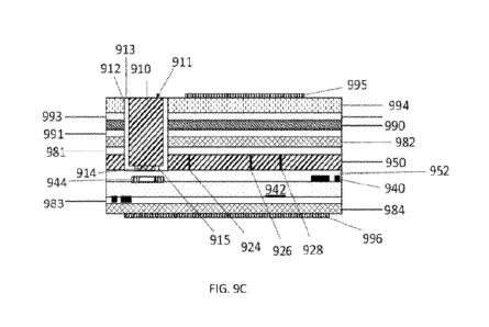
In yet another embodiment, depicted in FIGS. 9A-9C, the card includes a metal
layer 950, which may be formed from a metal foil, metal sheet, bulk metal, or
other
known metal. Metal layer 950 may comprise a plurality of discontinuities
extending
from the front surface 902 to the back surface 904 of the metal layer,
including at least
zo a first discontinuity 920 that defines a path from the card periphery to
opening 912 in
the metal layer for receiving the transponder chip module 910. In the
embodiment
depicted in FIGS. 9A-9C, other discontinuities 922, 924, 928 extend from the
periphery
to an endpoint that does not coincide with the opening 912. Another
discontinuity 926
extends from an intersection with discontinuity 920 to an endpoint that is
neither in the
opening nor at the periphery. Metal layer 950 may additionally comprise
additional
discontinuities, such as a second discontinuity that defines a path from the
card
periphery to opening (not shown in FIGS. 9A-9C, but akin to the respective
combinations of slits 504 and 554 or slits 564 and 574 depicted in FIG. 5A)
and bisects
the card into two discrete portions. The discontinuities may have any shape,
and may
include discontinuities that are incorporated into aspects of the aesthetic
design on one
or both faces of the card, including in coordination with printed features, or
formed in
the shape of alphanumeric characters, symbols, or the like.
In the embodiment depicted in FIGS. 9C, a booster antenna layer 942 comprises
a plurality of metallizations 940, 944 on a substrate (e.g. polyester) that
form a
booster antenna. Suitable booster antennas may also comprise a metal wire
antenna
disposed on a non-metal substrate. The metal portions of the antenna are
isolated
from the metal layer 950 by glue layer 952 separating the booster antenna and
the
CA 03165428 2022- 7- 20
WO 2021/158866
PCT/US2021/016741
- 20 -
metal layer. Booster antenna 942 is configured for communication with the
transponder chip module 910, and the transponder chip module 910 and the
booster
antenna 942 both comprise components in a circuit configured for wireless
communication with a card reader (not shown). The booster antenna may be
connected to the transponder chip module inductively, or with physical
connections
(e.g. wires, traces, or contacts). In exemplary embodiments, booster antenna!
layer
942 comprises a solid polyester layer (e.g. approximately 25 microns thick),
which may
be asymmetrically metalized on both sides, with vias through the polyester
connecting
respective metallizations disposed on opposite surfaces.
Reinforcing layer 982, such as fiberglass-reinforced epoxy laminate, such as
FR-
4, is disposed over the front surface 902 of metal layer 950, and a
reinforcing layer 984
of similar construction is disposed over the back surface 904 of the metal
layer 950 and
over the booster antenna layer 942. The reinforcing layer is not limited to
any
particular type of glass-reinforced epoxy laminate material, however,
including both
flame retardant (hence the designation "FR") and non-flame-retardant glass-
reinforced
epoxy laminates. The term "FR-4" may be used herein as shorthand to refer to a
reinforcing layer of any construction, including but not limited to flame
retardant and
non-flame-retardant fiber-reinforced epoxy laminates. The fibers in fiber-
reinforced
laminates may comprise fiberglass, polymeric fibers, or any other type of
fiber known
in the art for making fiber-reinforced structures. The term "fiber" as used
herein may
include any type of structure that includes fibers or filamentary members,
including
mesh or grid structures, woven structures, structures with randomly oriented
fibers, or
the like, without limitation. The FR-4 layers may be adhered to the respective
layers
by adhesive layers 981 and 983. The adhesive from the adhesive layers may
penetrate
and partially or entirely fill the discontinuities 924, 926, 928 during
formation of the
card. In some embodiments (not shown), antenna layer 942 and FR-4 layer 984
may
be inverted, with layer 984 as the outermost layer, with printed matter
printed directly
onto the outer printed sheet layer. It should be understood that in
embodiments in
which the antenna layer is adjacent the metal layer, the metallizations of the
antenna
are disposed on the opposite surface of the antenna substrate from the metal
layer, or
an insulating material (e.g. adhesive and/or a non-metal layer, such as
adhesive
disposed on a non-metal substrate) is disposed between the metallizations and
the
metal layer. In other embodiments, the metallizations may be embedded in the
FR-4
layers, such as using ultrasound techniques.
Although the term "metallizations" may typically be understood to refer to
coatings on the outside surface of a substrate, as used throughout this
application, the
term refers to any type of metal structure, and when referring to a booster
antenna
CA 03165428 2022- 7- 20
WO 2021/158866
PCT/US2021/016741
- 21 -
structure, refers to the metal construct of the antenna, regardless of form,
including
but not limited to structures created using etched films, coatings,
depositions, printing,
embedded wire, and the like.
Disposed above upper FR-4 layer 982, such as adhered by adhesive layer 991,
is disposed an optional, RF-friendly metal foil 990 (preferably configured
with a metallic
appearance), over which is adhered a plastic layer 994 (attached by adhesive
993).
Notably, the adhesive layers may be pre-formed together with the foil as a
composite,
and the foil composite hot stamped onto the FR-4, or rolled onto the FR-4. In
embodiments in which the foil is rolled on, the foil composite may comprise a
release
layer that is them removed before attaching the next layer. Printed content
995 is
disposed on plastic layer 994. In other embodiments, the printed content may
be
printed directly on the foil 990, and the plastic layer 994 / adhesive 993
omitted.
Other printed content 996 and/or a magnetic stripe (not shown) may be disposed
on
lower FR-4 layer 986. Embodiments in which the position of layers 994 and 990
in the
stack are inverted relative to one another (e.g. in switched positions so that
layer 900
is located relatively higher in the stack than layer 994) may also be
provided.
In the embodiment depicted in FIG. 9C, opening 912 extends through all of the
upper layers of the composite card such that a contact surface 911 of
transponder
module 910 is accessible from the top surface of the card. Such a construction
is
preferred in embodiments in which the transponder module is has contacts
configured
to be physically contacted by a card reader, such as a dual interface (DI)
module.
Constructions incorporating contactless-only modules may also be provided,
however,
in which the opening 912 does not extend to the top surface of the card.
Opening 912
may be filled with a non-metal plug 913 that isolates the transponder module
from the
metal layer. Plug 913 may have a hole 915 in the bottom for receiving a
downward
protruding region 914 of the transponder module having a relatively smaller
periphery
than the periphery of the widest portion of the module. The configuration of
the plug in
the metal layer may be in accordance with the teachings in U.S. Pat. Ser. No.
9,390,366, titled "METAL SMART CARD WITH DUAL INTERFACE CAPABILITY" and/or
10,318,859, titled DUAL INTERFACE METAL SMART CARD WITH BOOSTER ANTENNA, or
applications related thereto, incorporated herein by reference.
While not limited to any particular dimensions, an exemplary embodiment of the
aspect of the invention depicted in FIG. 9C may include the exemplary
thicknesses and
compositions as set forth in Table 1:
CA 03165428 2022- 7- 20
WO 2021/158866
PCT/US2021/016741
- 22 -
TABLE 1
Layer (Element number) Thickness (inches)
Ink (995) 0.0005 - 0.002
Plastic (994) 0.001-0.002
Adhesive (993) 0.001 - 0.003
Foil (990) ¨0.0005 (1- 12 urn)
Adhesive (991)* 0.001 - 0.003
FR-4 layer (982) 0.002-0.004
Adhesive (981)* 0.001 - 0.003
Metal (950) 0.01 - 0.02
Adhesive (952)* 0.001 - 0.003
FR-4 (984) 0.002-0.004
Adhesive (985)* 0.001 - 0.003
Antenna (942) 0.001 - 0.003
Plastic (997) 0.001 - 0.007
Ink (996) Negligible - 0.002
*optional (see below)
Although depicted in FIG. 9C, it should be understood that in many of the
interfaces between layers, the adhesive layer may be optional (or may not be a
discrete layer relative to the layers above or below). For example, as
described herein,
the FR-4 layers may be cast directly onto the metal layer. Non-metal layers
may be
laminated together in a way in which the material of the layer bonds to the
adjacent
layer(s) with or without adhesive. The antenna layer may be a discrete, self-
io supporting layer, or may comprise metallizations disposed directly on
the FR-4, such as
via metal foil that is etched, printed with metal ink, or wire embedded (e.g.
ultrasonically) into the FR-4 layer, as described further herein. In
embodiments in
which foil 990 is a "transfer foil," adhesive layer 991 is optional or may
represent an
adhesive layer integral to the matrix of the transfer foil 990 that bonds
directly to the
underlying layer. The positions in the stack of antenna layer 942 and FR-4
layer 984
may be inverted relative to one another, in which case plastic layer 997 may
be
omitted and ink layer 996 printed directly on FR-4 layer 984. Notably, the
foregoing
expresses only one embodiment, and other embodiments may contain more or fewer
layers.
CA 03165428 2022- 7- 20
WO 2021/158866
PCT/US2021/016741
- 23 -
In the embodiment depicted in FIGS. 9A-9C, booster antenna layer 942 includes
a plurality of nested semi-circular metallizations 944, which concentrate
induction, for
facilitating inductive coupling to transponder module 910. While shown with
inductive
coupling, in other arrangements, the booster antenna may have a physical
connection
to the transponder module.
Magnetic stripe 930 may be disposed over the bottom FR-4 layer 984. Other
card features, such as holograms, printing, 2-D codes (such as bar codes or QR
codes)
may also be incorporated in the card design, typically disposed over the
bottom FR-4
layer or on the top plastic layer.
Referring now to FIG. 10, an exemplary process for making a card as described
herein, such as for example the embodiment depicted in FIGS. 9A-96, may
include first
providing a sheet of metal 1000 that serves as metal layer 950 in the cross-
sections as
illustrated herein. The sheet is sized to be cut into a plurality of cards
along lines 1002,
1004, 1006, 1008. While FIG. 10 depicts only a portion of a sheet having only
four
cards, it should be understood that the sheet may be sized for cutting into
any number
of cards. What is important, regardless of the number of cards per sheet, is
that the
size of the sheet is preferably greater than the size of the card or cards to
be cut from
the sheet, so that when the sheet is sliced to form the desired
discontinuities, the sheet
remains intact.
The sheet may be inserted into a mold with layers of fiberglass or plastic
mesh
disposed over the metal layers, and then epoxy allowed to fill the mold,
thereby casting
epoxy over the top and/or bottom surfaces of the metal sheet to form FR-4
layers 982,
984 directly bonded to the metal layer, such in the embodiment depicted in
FIG. 9E. In
other embodiments, pre-formed FR-4 layers 982, 984 may be adhesively bonded to
the
top and/or bottom surfaces of the metal sheet, such as in the embodiment
depicted in
FIG. 9F.
More or fewer layers may be provided than are shown in FIGS. 9E and 9F,
including but not limited to layers described with respect to other
embodiments herein.
Likewise, more or fewer layers may be provided for any of the other
embodiments
discussed in any section of this disclosure. Similar element numbers for the
various
layers shown in FIGS. 9E and 9F are intended to refer layers with the same
function
and/or constructions as those referenced by the same number in other drawings,
but
the functions, layers, and locations in any of the depicted embodiments, are
not limited
to the arrangements shown. Those of skill in the art will recognize that a
number of
different arrangements are possible; however, certain of the embodiments as
discussed
herein may be particularly advantageous with respect to considerations of
cost,
durability, aesthetics, thickness minimization, or the like. The thicknesses
of the layers
CA 03165428 2022- 7- 20
WO 2021/158866
PCT/US2021/016741
- 24 -
as depicted in any of the figures should not be interpreted as an indication
of relative
thickness of the layers in actual constructions, as certain features may be
highlighted
or enhanced in the figures for illustration only.
Metallization 940 for the booster antenna may be included in the stack as part
of a discrete layer (e.g. 942) as depicted in FIGS. 9C and 9D, or may be
disposed
directly on or embedded beneath (not shown) one of the surfaces of the FR-4
layers, as
depicted in FIGS. 9E and 9F. One process for making an etched booster antenna
layer
typically comprises adhesively attaching a metal (e.g. copper) foil layer to
one surface
of the FR-4 layer, and then etching away unwanted portions of the foil to
leave the
desired antenna pattern. Other ways of disposing the antenna directly on or
into the
FR-4 include pattern vapor deposition, printing with conductive ink, and
embedding
copper wire into the FR-4 (such as using ultrasonic methods known in the art).
In embodiments in which a pre-formed layer of FR-4 is adhesively bonded to the
metal layer, the directly-disposed antenna may be disposed on the inside
surface of the
FR-4, and attached to the metal layer with a sufficient layer of adhesive
(such as with
layer 960, comprising adhesive layers 962, 964 disposed on opposite surfaces
of a non-
metal substrate 966) to insulate the metallizations 940 from the metal layer
950, as
depicted in FIG. 9F. In embodiments in which the metallizations for the
antenna
comprise wire embedded in the FR-4, such insulating layers may be omitted. In
other
embodiments, including those in which the FR-4 layers are directly cast onto
the metal
layer, such as in the embodiment depicted in FIG. 9E, the metallizations 940
for the
antenna may be formed on the outer surface of the FR-4 layer 984, and covered
with
another non-metal layer 997e. Embodiments in which one FR-4 layer is directly
cast,
and the other attached later may also be provided. Embodiments with a
metallized FR-
4 layer added to the metal as a discrete layer, instead of directly cast to
the metal,
may have metallizations on both sides of the FR-4 (optionally, connected with
vias
through the FR-4 layer), in which case the construction as depicted in FIG. 9F
may
include additional layer 997e on the outer surface of layer 984, as depicted
in FIG. 9E.
The covering layer 997e is typically an opaque plastic layer, such as plastic
laminated
(as depicted in FIG. 9F) or adhesively bonded to the FR-4 layer (not shown),
but the
outer layer may have any construction, particularly when adhesively bonded to
the FR-
4, including but not limited to a decorative layer of ceramic, wood, leather,
or even
another layer of metal, such as anodized metal. In embodiments in which the
metallizations for the antenna comprise wire embedded in the FR-4, the
additional non-
metal layer 997 may be omitted. insulation may be omitted.
Openings 1010 for accommodating the transponder module (corresponding to
opening 912 shown in other figures) may be milled in part or in whole into the
metal
CA 03165428 2022- 7- 20
WO 2021/158866
PCT/US2021/016741
- 25 -
sheet depicted in FIG. 10 at any time during the assembly process. For
example, the
metal may be precut prior to a step of directly casting the metal layer in
epoxy to form
the FR-4, so that epoxy fills the opening in the metal. In such
configurations, the
opening in the metal may be sufficiently larger than the transponder to form a
plug
that can be milled at a later step for receiving the module, with epoxy
disposed
between the transponder and the metal (and adhesive disposed between the
transponder and the epoxy). In embodiments wherein pre-formed FR-4 layers are
adhered to the metal, the metal may be cut at the same time as the
discontinuities,
and the remaining layers may have pre-cut holes that register with the holes
in the
metal, or the opening 1010 in the metal may be milled after the remaining
layers are
added, or the opening may be precut in the metal, and milled in the other
layers in a
later step.
The step of inserting the transponder in the opening may include inserting a
plug of non-metal material in the opening that surrounds the transponder. The
non-
metal material plug may comprise adhesive, or a combination of adhesive and
another
non-metal substance. In one embodiment, the plug and transponder may be pre-
assembled and adhesively bonded in the opening. In another embodiment, the
plug
may be placed in the opening first, and then milled to accommodate the
transponder.
The transponder inferface with the opening and process for creating it is not
limited to
zo any particular construction.
After the stack of layers has been assembled and the transponder modules
inserted, the sheet of cards may then be cut into a plurality of individual
card blanks,
and the individual card blanks further processed, including personalization,
as needed.
It should be understood that the transaction card of any of the embodiments
discussed
herein may be of any shape and size, including in a key fob configuration, as
described
herein with respect to FIGS. 8A-8B
It should be understood that although various concepts have been illustrated
using specific exemplary embodiments, the features of each of the embodiments
may
be mixed and matched as desired by those of skill in the art. For example, the
FR-4
and multi-discontinuity architecture as described with respect to FIGS. 9A-9C
may be
applied to a keychain embodiment, such as that illustrated in FIGS. 6A-8A.
Likewise,
aspects of the construction ¨ in particular, the absence of the metal layer
from the
payment circuit -- as described herein with reference to FIGS. 9A-9C in a
fiber-
reinforced epoxy embodiment, may also be featured in other constructions known
in
the art, without limitation, including but not limited to constructions using
other types
of overmolding materials or laminated layers, alone or in combination.
CA 03165428 2022- 7- 20
WO 2021/158866
PCT/US2021/016741
- 26 -
The foregoing embodiment is only an exemplary embodiment, and other
embodiments may include fewer or more layers, stacked in a different order,
and
attached to one another by any way known in the art, not limited to adhesive
connections. One or more of the functional layers may be formed from a sheet
coated
with adhesive and a peel-away release layer. In other embodiments, the glue
layers
may comprise glue disposed on both sides of a very thin sheet of polyester,
with
release layers disposed over both glue layers. In such embodiments, the
relevant
steps in a process for forming the card comprise removing a first release
layer,
attaching the exposed glue layer to an adjacent layer, and then removing the
second
release layer for attachment of a subsequent layer.
In the exemplary embodiment depicted in FIG. 9D, an exemplary card may be
formed from a premade laminate material comprising metal layer 950 with an
upper
FR-4 layer 982 and a lower FR-4 layer 984 attached to both surfaces thereof,
such as
may be formed by casting epoxy about a structural mesh placed over the metal
layer.
In one method for assembling the card, the premade laminate as described above
is
processed to create discontinuities 924, 926, and 928 and opening 912, from
the
bottom of the card. For example, a laser may be used for cutting from the
lower FR-4
984 layer through the metal layer 950 without penetrating the upper FR-4
layer,
thereby leaving the upper FR-4 layer 982 with sufficient integrity to provide
reinforcement for the card with the corresponding discontinuities. Additional
layers
may be added, as described herein in any embodiment, not limited to the stack
depicted in FIG. 9D. For example, RF-friendly foil 990 may be disposed over
the
premade laminate by a rolling or hot-stamp process, as described herein above,
the
remaining non-ink layers (e.g. booster antenna layer 942, optional lower
plastic layer
997, and any adhesive layers 983, 985, between adjacent layers) added, and
then the
stack laminated. Graphics layers 995 or 996 are printed on the outer surfaces
of the
laminated stack. The transponder module may be added before or after printing,
including milling the opening 912, inserting plug 913 in the opening 912,
milling an
opening in the plug, and inserting the module 910 in the plug. The plug and
module
may comprise a pre-made assembly, or may be assembled in situ. It should be
understood that the combination, sequence of layers in a stack, and methods
for
attaching layers to one another (e.g. with adhesive, or by lamination without
adhesive
between certain adjacent layers, depending upon composition of the layers) may
be
varied in any way known in the art.
One method of assembling the layers as depicted in the embodiments disclosed
herein may include creating the metal layer with discontinues and the opening
for
receiving the transponder module and separately preparing an FR-4 layer
without
CA 03165428 2022- 7- 20
WO 2021/158866
PCT/US2021/016741
- 27 -
metallizations, and an FR-4 layer with an etched metallized antenna, and
adhesively
sandwiching the metal layer between the FR-4 layers, resulting in the
structure
comprising layers 982, 960, 950, 960, 940, 984 as depicted in FIGS. 9F. The FR-
4
layer disposed on the top surface of the metal may have a pre-cut opening that
aligns
with the opening in the metal layer for the transponder module, or the FR-4
layer may
be milled after attachment to the metal layer to extend the opening to the top
surface
of the FR-4 layer. The plug is then disposed in the opening, other non-ink
layers (e.g.
plastic layers over one or both of the FR-4 layers) are added, and the card is
laminated
together.
In another embodiment, the process may include providing a premade laminate
of FR-4 on both sides of metal (e.g. layers 982, 950, 984 as depicted in FIG.
9E), and
then creating opening 912 and one or more discontinuities (e.g. 920, 922, 924,
926,
and 928) in the premade laminate. If desired, the discontinuities may be
formed so
that they penetrate only layer 984 and 950, but not layer 982 (as shown in
FIG. 9D).
In still another embodiment, the process may include providing the metal body
950,
creating opening 912 and one or more discontinuities (e.g. 920, 922, 924, 926,
and
928), placing mesh layers on the opposite surfaces of the metal layer, then
casting
epoxy over the mesh layers to form FR-4 layers 982, 984 bonded to metal layer
950.
The resulting layers 982, 950, 984 formed by either of the foregoing processes
are
zo then further processed, such as by placing a copper foil on one side of
the FR-4, and
unwanted portions etched away to form metallization 940. Notably, when
starting with
a premade laminate with discontinuities penetrating only one FR-4 layer and
the metal
layer (as depicted in FIG. 9D), the foil is preferably disposed on the FR-4
layer that
does not have discontinuities. In the alternative, the discontinuities may be
filled (such
as with a coating or another non-metal layer) prior to forming the
metallizations. The
foregoing preferences may be more desirable for etched or printed
metallizations, to
optimize integrity of the metallizations, than for embedded wire
metallizations, which
may be disposed in either FR-4 layer with fewer technical concerns. Layer 997e
is
added to cover the metallization (particularly in embodiments in which the
metallization
is exposed on the outside of the FR-4, resulting in the composition of layers
982, 950,
940, 984, 997e as depicted in FIG. 9E. Additional layers, including but not
limited to
layers 995 and 996 may optionally be included, as further described herein.
Although the invention is illustrated and described herein with reference to
specific embodiments, the invention is not intended to be limited to the
details shown.
Rather, various modifications may be made in the details within the scope and
range of
equivalents of the claims and without departing from the invention.
CA 03165428 2022- 7- 20