Note: Descriptions are shown in the official language in which they were submitted.
CA 03165945 2022-06-24
WO 2021/148323 PCT/EP2021/050818
METHOD OF MANUFACTURING A SOLAR CELL WITH INTEGRAL
COVERGLASS, AND CELL OBTAINED
Background of the invention
Technical field
The present invention relates in general to the field of solar cells and their
manufacture. As known, solar cells, or photovoltaic cells, are solid-state
(semiconductor)
electrical/electronic devices that convert the energy of sunlight incident on
them into
electricity via the photovoltaic effect. Solar cells are a type of
photoelectric cells, defined
as devices whose electrical characteristics, such as current and voltage, vary
when exposed
to light. In particular, the present invention relates to a method of
manufacturing a solar
cell with protection against low-energy protons (and other harmful
radiations), and a solar
cell obtained by such manufacturing method.
Overview of the state of the art
Solar cells, in particular those intended for uses in the space (hereinafter,
concisely,
"space solar cells") or at high altitude, need a protection capable of
shielding them from
low-energy protons (and other harmful radiations) and to protect them
mechanically.
Currently, a typical protection for solar cells consists of a glass (so-called
"coverglass" or "coverslip") in borosilicate doped with Cerium, which is glued
on the active
surface of each solar cell individually (the active surface of a solar cell
being the surface
which, in use, is intended to be exposed to sunlight), using a transparent
resin that reduces
the mechanical stress between the glass and the solar cell itself
In US 8,974,899 B1 a flexible hybrid coverglass for solar panels for
spacecraft is
described, consisting of small drops of fused silica or Cerium-doped
borosilicate glass
embedded in a matrix of traditional adhesives for the glass.
In US 2014/0007924 Al a stable screen to radiation for use in space
applications or
at high altitudes is described. The screen comprises a plurality of
overlapping planar glass
flakes which are held in a lamellar matrix of flexible polymeric material. The
flakes are
each comprised of a radiation-stable glass that is suitable for use in space
or high-altitude
applications. The flakes are arranged aligned with the lamellar direction of
the matrix.
US 2008/173349 Al discloses a light weight photovoltaic device for use in
stratospheric and outer space applications. The device includes a protective
surface coating
on the light incident side thereof. The protective coating does not
deleteriously affect the
CA 03165945 2022-06-24
WO 2021/148323 PCT/EP2021/050818
2
photovoltaic properties of the solar cell, is formed of a material which
protects said solar
cell from the harsh conditions in the stratospheric or outer space environment
in which the
photovoltaic device is adapted to be used, and remains substantially unchanged
when
exposed to the harsh conditions in the stratosphere or outer space. The
protective coating is
made of a spray coated silicone based material and is between 0.01 and 2 mil
thick. The
silicone based overcoat is prepared by a chemical spray process, using
commercial spray
coating equipment. The coating is then cured at elevated temperature. Suitable
silicone
based material is DOW CORNING 1-2620 (Low VOC Conformal Coating or
dispersion)
diluted with DOW CORNING 0S-30 solvent. An additional layer of a transparent
conductive material is deposited over the silicone layer to provide additional
protection in
the outer space environment, that is, added protection from UV radiation, as
well as it
allows for leakage of electrostatic charge, helping to prevent destructive ESD
events. The
transparent conductive layer includes layers of Indium-Tin-Oxide (ITO) or Zinc
oxide
(Zn0).
WO 84/02529 Al discloses that solar cells, particularly those positioned in
space,
require a coating to protect the solar cell against damage caused by solar
radiation. The
document discloses a protective coating which is a polyimide which has the
required
combination of properties of being colorless, transparent, relatively non-
brittle, having a
high degree of thermal stability and readily transmitting solar radiation
without appreciable
degradation. The coating is heat resistant and does not degrade significantly
when exposed
to ultraviolet radiation, and is highly effective in repelling low energy
proton particles. The
protective polyimide coating is a polymer having the recurring structural
unit. An anti-
reflective coating (a combination of TiOx and A1203, Ta205 or Si0x) is
deposited directly
on the active surface of the cell prior to application of the polyimide
protective coating.
Prior to the application of the polyimide coating, a primer coating (a silane
adhesion
promoter, such as aminopropyltrimethoxysilane) is applied to the upper surface
of the anti-
reflective coating. The primer coating increases the adhesion of the polyimide
coating to
the solar cell and particularly to the upper surface of the anti-reflective
coating.
Carol L. Martinez et al., "Test Results of Radiation Resistant Coatings
Integrated
with Flexible Substrate Materials and Active Solar Cells", 2016 IEEE 43rd
Photovoltaic
Specialists Conference (PVSC), 5 June 2016, p. 2586 ¨ 2591 discloses the
development of
radiation resistant UV reflector and wide-band anti-reflection (UVR/AR) and
proprietary
transparent conductive oxide (TCO) coatings for use with flexible coverglass
materials
such as Psuedo-Morphic Glass (PMG) and other silicone-based covers. Coatings
deposited
on flexible substrate materials were subjected to mechanical and space-
environment
CA 03165945 2022-06-24
WO 2021/148323 PCT/EP2021/050818
3
durability tests. Coated flexible substrates were then integrated (CIC'd) with
active IMM
and other cell types.
Roberta Campesato et al., "Effective Coating for High Efficiency Triple
Junction
Solar Cells", 2019 European Space Power Conference (ESPC), 30 September 2019,
p. 1 ¨
5 discloses that an important field to improve solar cell efficiency is the
optimization of the
antireflection coating (ARC) to allow more light to be converted; from a
theoretical point
of view this could increase the solar cell efficiency of 0.5%. Different ARC
designs have
been investigated, the most promising approaches being based on multi layers
or gradient
index approaches. These approaches have been theoretically and experimentally
optimized
.. to increase the photocurrent in the spectral range 300-1880 nm.
Summary of the invention
The Applicant has ascertained that the protective glasses currently used for
the
protection of solar cells, particularly space solar cells or solar cells for
high-altitude
applications, have some disadvantages, among which the lack of flexibility and
the high
cost of integration.
The protective glass to be used shall have specific characteristics depending
on the
particular type of solar cell and the particular application of the solar cell
itself Therefore,
the protective glasses shall be customized, made ad hoc. This is expensive
both in terms of
2 0 supply times and in terms of costs (so-called "non-recurring costs")
inherent in the design
of glasses having characteristics, such as size, from time to time different.
Furthermore, the
whole process for making and applying protective glasses to solar cells is
completely
detached from the manufacturing process of the solar cells themselves (which
is based on
semiconductor technology).
Concerning US 2008/173349 Al, the Applicant notices that the protection
against
the harsh conditions in the stratospheric or outer space environment is
provided by the
coating made of a spray coated silicone based material. The additional layer
of transparent
conductive material (ITO or ZnO) deposited over the silicone layer is
conductive because
it is devoted to provide added protection from UV radiation and to allow for
leakage of
electrostatic charge, helping prevent destructive ESD events.
The Applicant observes that the use of electrically conductive oxides like ITO
and
ZnO limits the thickness of the protective layer that can be formed, not to
hinder the
transparency of the protective layer to sunlight, which would be detrimental
to the
conversion efficiency of the solar cell. Thus, the protection against low-
energy protons is
limited. Moreover, the use of a transparent conductive material limits the
suitable materials,
not allowing a choice of the material with the better refractive index.
CA 03165945 2022-06-24
WO 2021/148323 PCT/EP2021/050818
4
In respect of WO 84/02529 Al, the Applicant notices that the protection for
the
solar cell is given by the polyimide coating. The primer coating serves for
increasing the
adhesion of the polyimide coating to the solar cell and particularly to the
upper surface of
the anti-reflective coating, not for the protection for the solar cell. The
Applicant further
notices that in WO 84/02529 Al a thin (thickness less than 1 p.m) anti-
reflective coating
layer (a combination of TiOx and A1203, Ta205 or Si0x) is deposited directly
on the active
surface of the cell prior to application of the polyimide protective coating,
i.e. the anti-
reflective coating is under the polyimide coating (and under the primer
coating).
The Applicant notices that in the paper by Carol L. Martinez et al. the
coatings
deposited over the PMG and other silicon-based covers (Fig. 1 of the paper)
are thin-film
layers having the purpose of protecting the solar cell against exposure to
atomic oxygen
and UV radiation. The coatings must resist to (not protect against) the
ionizing radiation
(gamma rays, X rays, charge carriers ¨ electrons and protons ¨ trapped by the
Earth
magnetic field) existing in space environment. The coatings, being anti-
reflective or UV-
reflective, are typically thin (Figs. 2 and 3 of the paper report thicknesses
of 8 nm, 15 nm
and 16 nm for the transparent conductive oxide ¨ TCO ¨ coating; it can be
appreciated that
even an increase of few nanometers - from 8 nm to 15 nm to 16 nm - in the TCO
coating
thickness already causes a significant decrease in the spectral transmittance
of the coatings
in the range of wavelengths from 300 nm to 500 nm).
The paper by Roberta Campesato et al. deals with anti-reflective coatings
deposited
directly on the active surface of the solar cell. The purpose of the anti-
reflective coatings
is to minimize the reflection of sun light. The Applicant observes that the
anti-reflective
coatings, being anti-reflective, are typically thin.
The Applicant has faced the problem of identifying a solution to the problem
of
protecting solar cells against low-energy protons (and other harmful
radiations)
encountered in space environment and at high altitude in atmosphere, which
does not
involve the drawbacks associated with the use of protective glasses.
The Applicant has found that it is possible to provide a protection for a
solar cell,
against low-energy protons (and other harmful radiations) encountered in space
environment and at high altitude in atmosphere, by direct formation (e.g., by
deposition of
material), on the active surface of the solar cell (the surface which, in use,
is intended to be
exposed to sunlight), of one or more layers of protective material(s),
suitable to protect the
solar cell against low-energy protons and other radiations harmful to the
solar cell
(hereinafter, for the sake of brevity, also called "protective material(s)"),
of suitable
thickness (particularly, thick enough to stop protons having an energy of at
least 200 KeV
(0.2 MeV), for example, at least 2 p.m) and transparent to the electromagnetic
radiation (in
CA 03165945 2022-06-24
WO 2021/148323 PCT/EP2021/050818
particular, solar radiation) in a range of frequencies in which the solar cell
is able to carry
out the photovoltaic conversion, which perform the same function as the known
protective
glasses.
Such protective material(s) layers may comprise or consist of oxide layers,
5
particularly non-conductive oxide layers. For the purposes of the present
disclosure, a
"non-conductive" material is to be intended as meaning a material having an
electrical
conductivity of less than about iO3
Examples of suitable non-conductive oxides that can be used as protective
materials
include Silicon oxide (5i02), Aluminum oxide (A1203), Tantalum oxide (Ta205),
Niobium
oxide (Nb2O5), Yttrium oxide (Y203), Titanium oxide (TiO2), Scandium oxide
(5c203),
Cerium oxide (Ce02), Hafnium dioxide (Hf02), Tin dioxide (5n02), LaTiO3.
In addition to non-conductive oxides, other non-conductive materials,
transparent
in the frequency range used by the solar cell to make the photovoltaic
conversion of the
electromagnetic radiation (in particular, the sunlight), can be used to form
the protective
material layer(s), such as for example Magnesium fluoride (MgF2), Cerium
fluoride (CeF,),
Zinc sulphide (ZnS), Silicon nitride (Si3N4).
Such layers of protective material(s) can be formed (e.g., by deposition of
material)
over the (active surface of the) solar cell directly or by interposing an
adhesive layer, e.g. a
layer of a resin between the (active surface of the) solar cell and the layers
of protective
material(s). It is also possible to form, above the (active surface of the)
solar cell, a
combination of stacked layers of resin and protective materials, for example a
layer of
protective material formed (e.g., by deposition of material) directly on the
(active surface
of the) solar cell, followed by a resin layer formed on the layer of
protective material, and,
on the resin layer, an additional layer of protective material.
The use of non-conductive materials to form the protective layers makes it
possible
to form relatively thick protective layers (thicker than in case electrically
conductive oxide
layers are used) while ensuring a high level of transparency to the
electromagnetic radiation
(in particular, solar radiation) in the range of frequencies in which the
solar cell is able to
carry out the photovoltaic conversion. Thicker protective layers are more
effective in
blocking low-energy protons and other radiations harmful for the solar cell.
In addition, the use of non-conductive materials (instead of electrically
conductive
oxide layers) as protective layers widens the range of suitable materials that
can be chosen,
allowing a better choice of the refractive index of the material chosen to
form the protective
layer.
As mentioned, the layers of protective material(s) can for example be formed
by
deposition techniques, for example by resorting to any known technique of
Physical Vapor
CA 03165945 2022-06-24
WO 2021/148323 PCT/EP2021/050818
6
Deposition ("PVD"), such as thermal evaporation, electron gun, Pulsed Laser
Deposition
("PLD"), cathodic sputtering (or cathodic vaporization) etc..
The adhesive (resin) layer or layers can be made of a resin of the same type
as the
resins that are normally used to glue the coverglass to the solar cell. The
resin used can be
a transparent silicone adhesive material, for example the material known
commercially as
ELASTOSIL S 695 or S 690, or the elastomeric silicone material commercially
known as
DC93-500 manufactured by Dow Corning .
The layers of protective material(s) also protect the resin layer(s) against
low energy
protons, preventing the resin layer(s) from degradation consequent to exposure
to low
energy proton radiation.
In accordance with an aspect of the present invention, a method of
manufacturing a
solar cell is provided, comprising:
- providing a solar cell having an active surface intended, in use, to be
exposed to sunlight for performing photovoltaic conversion, and
- forming, in correspondence of said active surface, a protection against low-
energy protons and other radiations harmful to the solar cell.
Said forming a protection includes:
- form a resin layer, and
- forming by means of deposition of material on the resin layer a layer of
a
non-conductive protective material, transparent in an electromagnetic
radiation
frequency range in which the solar cell is intended to perform the
photovoltaic
conversion, over the resin layer.
Forming by means of deposition of material comprises a physical vapor
deposition - PVD - process or processes, particularly thermal evaporation,
electron
beam, pulsed laser deposition - PLD -, sputtering.
In possible embodiments, said resin layer can be formed directly on the active
surface of the solar cell.
In possible embodiments, the method may further comprise:
- forming, by means of deposition of material, a further layer of
protective
material interposed between the resin layer and the active surface of the
solar cell.
In possible embodiments, said forming by means of deposition of material a
further
layer of protective material interposed between the resin layer and the active
surface of the
solar cell may comprise a physical vapor deposition - PVD - process or
processes, for
example thermal evaporation, electron beam, pulsed laser deposition - PLD -,
sputtering.
In possible embodiments, said layer or layers of protective material can
comprise or
consist of oxide layers, in particular one or more layers of Silicon oxide
(5i02), Aluminum
CA 03165945 2022-06-24
WO 2021/148323 PCT/EP2021/050818
7
oxide (A1203), Tantalum oxide (Ta205), Niobium oxide (Nb2O5), Yttrium oxide
(Y203),
Titanium oxide (TiO2), Scandium oxide (5c203), Cerium oxide (Ce02), Hafnium
dioxide
(Hf02), Tin dioxide (5n02), LaTiOõ and other materials transparent in the
frequency range
used by the solar cell to carry out the photovoltaic conversion, including
Magnesium
fluoride (MgF2), Cerium fluoride (CeF,), Zinc sulphide (ZnS), Silicon nitride
(Si3N4).
In possible embodiments, said phase of forming a resin layer may include king
a
deposition process.
In possible embodiments, the method can include:
- forming alternating layers of resin and protective material repeated
several
times.
In possible embodiments, the method can include:
-forming anti-reflective layers atop of the top protection layer.
Preferably, said layer of protective material, or at least one of the layers
of protective
material, has a thickness greater than about 2 [tm.
In accordance with another aspect of the present invention, a solar cell is
provided
comprising an active surface intended, in use, to be exposed to sunlight for
performing
photovoltaic conversion, at which active surface a protection against low-
energy protons
and other radiations harmful to the solar cell is provided. The solar cell is
obtained by the
manufacturing method in accordance with the above aspect of the present
invention.
2 0 Said
protection against low-energy protons and other harmful radiations can include
at least one resin layer and, above the resin layer, at least one layer of a
protective material
against low-energy protons and other harmful radiations for the solar cell,
transparent to
solar radiation in a range of frequencies used by the solar cell to carry out
the photovoltaic
conversion. Said at least one layer of protective material is a layer of
deposited, non-
conductive material, that can be obtained by deposition of material, for
example, physical
deposition from vapor phase - Physical Vapor Deposition (PVD) - for example,
thermal
evaporation, electron beam, Pulsed Laser Deposition (PLD), sputtering.
Said at least one layer of protective material can comprise or consist of
oxide layers,
in particular one or more layers of Silicon oxide (5i02), Aluminum oxide
(A1203), Tantalum
oxide (Ta205), Niobium oxide (Nb2O5), Yttrium oxide (Y203), Titanium oxide
(TiO2),
Scandium oxide (5c203), Cerium oxide (Ce02), Hafnium dioxide (Hf02), Tin
dioxide
(5n02), LaTiOõ and other materials transparent in the frequency range used by
the solar
cell to carry out the photovoltaic conversion, including Magnesium fluoride
(MgF2),
Cerium fluoride (CeF,), Zinc sulphide (ZnS), Silicon nitride (Si3N4).
Preferably, said at least one layer of a protective material has a thickness
greater
than 2 [tm.
CA 03165945 2022-06-24
WO 2021/148323 PCT/EP2021/050818
8
The one or more layers of protective material(s) perform the protective
function of
the (active surface of) solar cell, blocking low-energy protons and other
harmful radiations
for the solar cell that are encountered in space environment and at high
altitudes in
atmosphere. The layer or layers of resin are useful to reduce the mechanical
stress due to
different coefficients of thermal expansion of the materials used, ensuring,
in this way, also
a better adhesion of the layer of protective material on the surface of the
device.
Thanks to the present invention, it is possible to realize a solar cell
protection against
low-energy protons and other harmful radiations to the solar cell by means of
a method
which is integrated in the traditional solar cell manufacturing process itself
(based on
semiconductor technology). The protection obtained in this way is by far
advantageous
compared to that obtainable through the application of the usual coverglasses
since it does
not present the problems related to the ad hoc sizing of the protection
glasses, particularly
in terms of area. Furthermore, the thickness of the protection is easily
adaptable to the
specific needs deriving from the specific application of the solar cell. The
manufacturing
.. costs of solar cells are consequently significantly reduced. Last but not
least, the protection
achieved by layers of protective material(s) formed integrally with the solar
cell guarantees
the flexibility of the solar cell itself, a feature (not achievable with
traditional protective
glasses) which is particularly useful in the case of thin solar cells.
Brief description of the drawings
These and other features, as well as these and other advantages, of the
present
invention will be made more apparent by reading the following detailed
description of some
of its possible embodiments, exemplary and by no means limitative; in the
following
description reference will be made, for a better intelligibility, to the
attached figures, in
which:
Figures 1A to 1C show three stages of a method of manufacturing a solar cell
according to an embodiment of the present invention;
Figures 2A to 2D show four steps of a method of manufacturing a solar cell
according to another embodiment of the present invention, and
Figure 3 is a diagram showing the "cut-off" energy as a function of the
thickness
and the type of protective material used, for certain types of exemplary
protective materials.
It should be noted that the drawings shown in the figures are schematic and
not
necessarily executed to scale. In particular, some details of the drawings can
be very
exaggerated (compared to their real size) for purely explanatory purposes.
Detailed description of exemplary embodiments of the present invention
CA 03165945 2022-06-24
WO 2021/148323 PCT/EP2021/050818
9
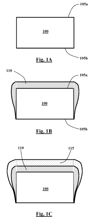
With reference to the drawings, in Figures 1A to 1C three phases of a method
of
manufacturing a solar cell according to an embodiment of the present invention
are shown.
Reference 100 denotes a solar cell, such as a space solar cell. The solar cell
100 can
for example be a cell in compounds of groups III and V of the periodic table
of the elements
solar cell "), for example in gallium arsenide (GaAs) or in Indium and Gallium
phosphide (InGaP). The solar cell 100 can be a single-junction solar cell,
i.e. with a single
pn junction, or a multi-junction solar cell, with two or more pn junctions,
for example a
triple junction solar cell (comprising three pn junctions). The steps of the
manufacturing
process of the solar cell 100 are neither shown nor described as they are
known to those
1 0 skilled in the art.
The solar cell 100 has an active surface 105a (the surface of the solar cell
which, in
use, is intended to be exposed to sunlight for allowing the solar cell
performing the
photovoltaic conversion) and an opposite, non-active surface 105b (which in
use is not
exposed to sunlight) in correspondence of which the solar cell 100 is applied
to a support
panel (not shown in the drawings).
As shown in Figure 1B, on the active surface 105 of the solar cell 100 (the
surface
of the solar cell which, in use, is intended to be exposed to sunlight) a
layer of resin 110
transparent to sunlight is formed. The resin may for example be of the same
type as the
resins which in the art are used to glue the protective coverglass to the
solar cell. For
2 0 example, the resin used may be a transparent silicone adhesive
material, for example the
material commercially known as Elastosil S 695 or S 690, or the elastomeric
silicone
material commercially known as DC93-500 manufactured by Dow Corning . The
resin
layer 110 can for example be formed by means of any deposition technique used
for the
integration of space solar cells (with the usual steps which will not be
described as they are
known to those skilled in the art). In Figure 1B it is also shown (in a very
exaggerated way
compared to the actual dimensions) how, as a consequence of the formation
process of the
resin layer 110 by deposition, the material of the resin layer 110 protrudes
from the edges
of the active surface 105a of the solar cell 100 and descends along the
lateral walls of the
solar cell 100 itself, covering them (in a gradually decreasing way as one
moves away from
the active surface 105). The resin layer 110 can for example have a thickness
ranging from
some tens of microns to about 100 pm.
Turning to Figure 1C, on the resin layer 110 a layer of protective material
115 is
formed which is transparent to sunlight (in the range of wavelengths for which
the solar
cell is intended to perform the photoelectric conversion) but capable of
blocking low-
energy protons and other radiations harmful to the solar cell 100. The
protective material
layer 115 is a layer in a non-conductive material. The protective material
layer 115 may
CA 03165945 2022-06-24
WO 2021/148323 PCT/EP2021/050818
comprise or consist of a layer of a non-conductive oxide, e.g. Silicon oxide
(5i02) or oxides
of other elements, or other non-conductive materials, transparent in the
frequency range
used by the solar cell to perform the photovoltaic conversion. For example, in
addition to
Silicon oxide (5i02), the protective material layer 115 may comprise or
consist of
5
Aluminum oxide (A1203), Tantalum oxide (Ta205), Niobium oxide (Nb2O5), Yttrium
oxide
(Y203), Titanium oxide (TiO2), Scandium oxide (5c203), Cerium oxide (Ce02),
Hafnium
dioxide (Hf02), Tin dioxide (5n02), LaTiOõ Indium Tin oxide (also known as
Indium-
doped Tin Oxide or ITO), or other transparent materials in the frequency range
used by the
solar cell to carry out the photovoltaic conversion, such as for example
Magnesium fluoride
10
(MgF2), Cerium fluoride (CeF3), Zinc sulphide (ZnS), Silicon nitride (Si3N4).
The layer of
protection material 115 has a suitable thickness, chosen so as to provide, in
use, the desired
protection of the solar cell 100.
The shielding power (so-called "Stopping Power") that the layer of protective
material 115 has on low-energy protons depends, in addition to the thickness
of this layer,
on the density and on the atomic composition of the protective material used.
The cut-off
energy (maximum energy of the protons that the material is able to completely
shield), as
a function of the thickness of the layer of protective material 115 used, can
be obtained
using models and calculation codes known in the literature (for example, SRIM,
www.srim.org). Figure 3 shows the cut-off energy performance as a function of
the
thickness of the protective material layer for three types of exemplary
protective materials:
5i02, A1203, Ta205.
For example, if the layer of protective material 115 has a thickness of at
least 2 p.m,
the protons with energy less than or equal to 0.2 MeV are shielded.
The layer of protective material 115 can for example be formed by means of
deposition techniques, using for example any known technique of Physical Vapor
Deposition (PVD), such as thermal evaporation, electronic beam, Pulsed Laser
Deposition
(PLD), cathodic sputtering (or cathodic vaporization, simply "sputtering")
etc. Similarly to
Figure 1B, Figure 1C also shows (in a very exaggerated way compared to the
actual
dimensions) how, as a consequence of the process of forming the layer of
protective
material 115 by deposition, the material of the layer of protective material
115 protrudes
from the edges of the active surface 105a of the solar cell 100 and descends
along the side
walls of the solar cell 100 itself, covering (in a decreasing way as one moves
away from
the active surface 105 ) the same side walls (which had already been covered
by the material
of the resin layer 110).
The manufacture of the solar cell takes place with the usual steps, which will
not be
described as they are known to those skilled in the art.
CA 03165945 2022-06-24
WO 2021/148323 PCT/EP2021/050818
11
The adhesive resin layer 110 has essentially no protection function of the
solar cell
against low energy protons. The presence of the adhesive resin layer 110
interposed
between the layer of protective material 115 and the active surface 105a of
the solar cell
100 helps to reduce the mechanical stresses between the layer of protective
material 115
and the solar cell 100.
The layer of protective material 115 present above the resin layer 110, in
addition
to carrying out the function of protection against low-energy protons and
other radiations
harmful to the solar cell 100, avoids the phenomenon of yellowing
("darkening") of the
resin layer 110 which on the contrary could affect the latter as a result of
the exposure to
1 0 ultraviolet radiation in the use of the solar cell. The layer of
protective material 115 also
protects the resin layer 110 against low energy protons, avoiding the
degradation of the
resin layer 110 consequent to exposure to low energy proton radiation.
In Figures from 2A to 2D four phases of a method of manufacturing a solar cell
according to another embodiment of the present invention are shown.
Starting from the solar cell 100 shown in Figure 2A (as in the embodiment
described above, the solar cell 100 can for example be a III-V solar cell, for
example in
GaAs or InGaP, single junction or multi-junction), on the active surface 105a
of the solar
cell 100 a first layer of protective material 215a is formed, as shown in
Figure 2B. The
layer of protective material 215a is transparent to sunlight (in the range of
wavelengths for
2 0 which the solar cell is intended to perform the photoelectric
conversion). The protective
material layer 115 is a layer in a non-conductive material. The layer of
protective material
215a can, for example, include or consist of a layer of 5i02or oxides of other
elements, or
other non-conductive materials transparent in the range of frequencies used by
the solar cell
to make the photovoltaic conversion. In addition to Silicon oxide (5i02), the
protective
material layer 215a may comprise or consist of Aluminum oxide (A1203),
Tantalum oxide
(Ta205), Niobium oxide (Nb2O5), Yttrium oxide (Y203), Titanium oxide (TiO2),
Scandium
oxide (5c203), Cerium oxide (Ce02), Hafnium dioxide (Hf02), Tin dioxide
(5n02), LaTiO3,
or other transparent materials in the frequency range used by the solar cell
to perform the
photovoltaic conversion, such as for example Magnesium fluoride (MgF2), Cerium
fluoride
(CeF,), Zinc sulphide (ZnS), Silicon nitride (Si3N4).
The thickness of the layer of protective material 215a can be sized as a
function of
the energy of the protons that the oxide layer must be able to shield. The
layer of protective
material 215a can for example be formed by deposition techniques, such as
those
mentioned in the description of the previous embodiment. In Figure 2B it is
also shown
(much exaggerated compared to the actual size) as, in consequence of the
forming process
of the protective material layer 215a by deposition, the material of the
protective material
CA 03165945 2022-06-24
WO 2021/148323 PCT/EP2021/050818
12
layer 215a overlaps the edge of the active surface 105a of the solar cell 100
and descends
along the side walls of the solar cell 100 itself, covering them (in a
gradually decreasing
way as one moves away from the active surface 105).
A sunlight transparent resin layer 210 is formed on the first layer of
protective
material 215a, as shown in Figure 2C. The resin layer 210 can for example be
made as
described in relation to the resin layer 110 of the previous embodiment. Also
in this case,
Figure 2C also shows (in a very exaggerated way compared to the actual
dimensions) how,
as a consequence of the formation process of the resin layer 210 by
deposition, the material
of the resin layer 210 protrudes from the edges of the surface activates 105a
of the solar
cell 100 and descends along the side walls of the solar cell 100 itself,
covering (in a
gradually decreasing extent as one moves away from the active surface 105) the
side walls
themselves (which had already been covered by the material of the material
layer protection
215a).
A second layer of sunlight-transparent protective material 215b is formed over
the
resin layer 210, as shown in Figure 2D. The second layer of protective
material 215b is a
layer in a non-conductive material. The second layer of protective material
215b can for
example comprise or consist of a layer of SiO2 or oxides of other elements, or
other non-
conductive materials transparent in the range of frequencies used by the solar
cell to carry
out the photovoltaic conversion. Also in this case, in addition to SiO2, the
layer of protective
material 215b can comprise or consist of Aluminum oxide (A1203), Tantalum
oxide (Ta205),
Niobium oxide (Nb2O5), Yttrium oxide (Y203), Titanium oxide (TiO2), Scandium
oxide
(5c203), Cerium oxide (Ce02), Hafnium dioxide (Hf02), Tin dioxide (51102),
LaTiOõ or
other transparent materials in the frequency range used by the solar cell to
perform the
photovoltaic conversion, such as for example Magnesium fluoride (MgF2), Cerium
fluoride
(CeF,), Zinc sulphide (ZnS), Silicon nitride (Si3N4). The layer of protective
material 215b
can for example be formed by the same deposition techniques used to form the
first layer
of protective material 215a. In Figure 2D it is also shown (much exaggerated
compared to
the actual size) as, in consequence of the protective material layer formation
process 215b
by deposition, the material of the protective material layer 215b overlaps the
edge of the
active surface 105a of the solar cell 100 and descends along the side walls of
the solar cell
100 itself, covering (in a gradually decreasing extent as one moves away from
the active
surface 105) the side walls themselves (which had already been covered by the
material of
the first layer of protective material 215a and the material of the resin
layer 210).
The presence of the resin layer 210 helps to reduce the mechanical stress
between
the layers of protective material 215a and 215b and the solar cell 100.
CA 03165945 2022-06-24
WO 2021/148323 PCT/EP2021/050818
13
The layers of protective material 215a and 215b perform the function of
protection
against low-energy protons and other harmful radiations to the solar cell 100.
The second layer of protective material 215b which covers the resin layer 210
avoids the phenomenon of yellowing (darkening) resulting from exposure to
ultraviolet
radiation.
The layers of protective material 215a and 215b also protects the resin layer
210
against low energy protons, avoiding the degradation of the resin layer 110
consequent to
exposure to low energy proton radiation.
Other embodiments of the present invention are possible, for example by
iterating
the structure shown in Figure 2D by forming one or more further pairs of resin
layer 210
and protective material layer 215b above the protective material layer 215b.
The materials used to form the resin layers 110, 210, and the materials used
to form
the layers of protective material(s) 115, 215a, 215b may be different from the
materials
previously indicated by way of example, and the thicknesses of these layers
may vary from
the indicated thicknesses.
Over the last layer of protective material (at the top of the solar cell) it
is possible
to deposit a layer or a multilayer with an anti-reflective function.
* * * * *