Note: Descriptions are shown in the official language in which they were submitted.
CA 03167019 2022-07-06
WO 2021/178207
PCT/US2021/019641
Digital-to-Analog Converter Circuitry for a Stimulator Device
Having Non-Linear Amplitude Adjustment
FIELD OF THE INVENTION
[001] This application relates to implantable stimulator devices, and in
particular to
the current source circuitry used to provide therapeutic currents at the
electrodes of the
device.
INTRODUCTION
[002] Implantable neurostimulator devices are devices that generate and
deliver
electrical stimuli to nerves and tissues for the therapy of various biological
disorders, such as
pacemakers to treat cardiac arrhythmia, defibrillators to treat cardiac
fibrillation, cochlear
stimulators to treat deafness, retinal stimulators to treat blindness, muscle
stimulators to
produce coordinated limb movement, spinal cord stimulators to treat chronic
pain, cortical
and deep brain stimulators to treat motor and psychological disorders, and
other neural
stimulators to treat urinary incontinence, sleep apnea, shoulder subluxation,
etc. The
description that follows will generally focus on the use of the invention
within a Spinal Cord
Stimulation (SCS) system or a Deep Brain Stimulation (DBS) system. However,
the present
invention may find applicability with any implantable neurostimulator device
system.
[003] An SCS or DBS system typically includes an Implantable Pulse
Generator
(IPG) 10 shown in Figure 1. The IPG 10 includes a biocompatible device case 12
that holds
the circuitry and a battery 14 for providing power for the IPG to function.
The IPG 10 is
coupled to tissue-stimulating electrodes 16 via one or more electrode leads
that form an
electrode array 17. For example, one or more percutaneous leads 15 can be used
having ring-
shaped or split-ring electrodes 16 carried on a flexible body 18. In another
example, a paddle
lead 19 provides electrodes 16 positioned on one of its generally flat
surfaces. Lead wires 20
within the leads are coupled to the electrodes 16 and to proximal contacts 21
insertable into
lead connectors 22 fixed in a header 23 on the IPG 10, which header can
comprise an epoxy
for example. Once inserted, the proximal contacts 21 connect to header
contacts 24 within
the lead connectors 22, which are in turn coupled by feedthrough pins 25
through a case
feedthrough 26 to stimulation circuitry 28 within the case 12.
[004] In the illustrated IPG 10, there are thirty-two electrodes (E1-E32),
split
1
CA 03167019 2022-07-06
WO 2021/178207
PCT/US2021/019641
between four percutaneous leads 15, or contained on a single paddle lead 19,
and thus the
header 23 may include a 2x2 array of eight-electrode lead connectors 22.
However, the type
and number of leads, lead connectors, and electrodes in an IPG is application-
specific and
therefore can vary. The conductive case 12 can also comprise an electrode
(Ec). In a SCS
application, the electrode lead(s) are typically implanted in the spinal
column proximate to
the dura in a patient's spinal cord, and the IPG is typically implanted under
the skin in the
buttocks region. In a DBS application, the electrode leads are typically
implanted in
particular regions of the brain, and the IPG is typically implanted under the
skin under the
clavicle (collarbone). In other IPG examples designed for implantation
directly at a site
requiring stimulation, the IPG can be lead-less, having electrodes 16 instead
appearing on the
body of the IPG 10 for contacting the patient's tissue. The IPG lead(s) can be
integrated with
and permanently connected to the IPG 10 in other solutions. The goal of
neurostimulation
therapy is to provide electrical stimulation from the electrodes 16 to
alleviate a patient's
symptoms, such as chronic back pain in an SCS application, or tremors in a DBS
application.
[005] IPG 10 can include an antenna 27a allowing it to communicate bi-
directionally
with a number of external devices used to program or monitor the IPG, such as
a hand-held
patient remote controller or a clinician programmer. See, e.g., U.S. Patent
Application
Publications 2015/0360038 and 2015/0231402. Antenna 27a as shown comprises a
conductive coil within the case 12, although the coil antenna 27a can also
appear in the
header 23. When antenna 27a is configured as a coil, communication with
external devices
preferably occurs using near-field magnetic induction. IPG 10 may also include
a Radio-
Frequency (RF) antenna 27b. In Figure 1, RF antenna 27b is shown within the
header 23, but
it may also be within the case 12. RF antenna 27b may comprise a patch, slot,
or wire, and
may operate as a monopole or dipole. RF antenna 27b preferably communicates
using far-
field electromagnetic waves, and may operate in accordance with any number of
known RF
communication standards, such as Bluetooth, Zigbee, MICS, and the like. If the
battery 14 is
rechargeable, the IPG 10 may further include a charging coil (not shown) to
wirelessly
receive energy from an external charging device.
[006] Stimulation in IPG 10 is typically provided by pulses, and each pulse
may
include a number of phases, as shown in the example of Figure 2A. Stimulation
parameters
for the pulses typically include magnitude (current I, although a voltage
amplitude V can also
be used); frequency (F); pulse width (PW) of the pulses or of its individual
phases; the
electrodes 16 selected to provide the stimulation; and the polarity of such
selected electrodes,
i.e., whether they act as anodes that source current to the tissue or cathodes
that sink current
2
CA 03167019 2022-07-06
WO 2021/178207
PCT/US2021/019641
from the tissue. These and possibly other stimulation parameters taken
together comprise a
stimulation program that the stimulation circuitry 28 in the IPG 10 can
execute to provide
therapeutic stimulation to a patient.
[007] In the example of Figure 2A, electrode E4 has been selected as an
anode
(during its first phase 30a), and thus provides pulses which source a positive
current of
magnitude +I to the tissue. Electrode E5 has been selected as a cathode (again
during first
phase 30a), and thus provides pulses which sink a corresponding negative
current of
magnitude -I from the tissue. This is an example of bipolar stimulation, in
which only two
lead-based electrodes are used to provide stimulation to the tissue (one
anode, one cathode).
However, more than one electrode may be selected to act as an anode at a given
time, and
more than one electrode may be selected to act as a cathode at a given time.
The case
electrode Ec (12) can also be selected as an electrode, or current return, in
what is known as
monopolar situation.
[008] IPG 10 as mentioned includes stimulation circuitry 28 to form
prescribed
stimulation at a patient's tissue. Figure 3A shows an example of stimulation
circuitry 28,
which includes Digital-to-Analog converters (DACs) that provide an analog
currents at the
electrodes in accordance with specified magnitudes as explained further below.
The
stimulation circuitry 28 depicted includes a plurality of current source
circuits (PDACs) and a
plurality of current sink circuits (NDACs), so named in accordance with the
Positive
(sourced, anodic) and Negative (sunk, cathodic) currents they respectively
issue. In the
example shown, a NDACi/PDACi pair is dedicated (hardwired) to a particular
electrode node
ei, each of which is connected to one of the electrodes Ei 16 via DC-blocking
capacitors Ci
38, for the reasons explained below. The stimulation circuitry 28 in this
example also
supports selection of the conductive case 12 as an electrode (Ec 12), which
case electrode is
typically selected for monopolar stimulation. While the PDACs and NDACs are
assumed in
this disclosure to comprise current sources able to provide a prescribed
constant current, they
can also comprise voltage sources able to provide a prescribed constant
voltage.
[009] Power for the stimulation circuitry 28 is provided by a compliance
voltage
VH. As described in further detail in U.S. Patent Application Publication
2013/0289665, the
compliance voltage VH can be produced by a compliance voltage generator 29,
which can
comprise a circuit used to boost the battery 14's voltage (Vbat) to a voltage
VH sufficient to
drive the prescribed current I through the tissue R. The compliance voltage
generator 29 may
comprise an inductor-based boost converter or can comprise a capacitor-based
charge pump,
as explained in U.S. Patent Application Publication 2018/0071512 for example.
Because the
3
CA 03167019 2022-07-06
WO 2021/178207
PCT/US2021/019641
resistance of the tissue is variable, VH may also be variable, and can be as
high as 18 Volts in
one example. Although not shown, U.S. Patent Application Publications
2018/0071520
explains that the PDACs and the NDACs can be powered by different power supply
domains.
For example, the PDACs can be powered using a first power supply domain, which
includes
VH as the high supply and VH-Vcc as the low supply (both of which may vary,
because VH
may vary). The NDACs can be powered using a second power supply domain, which
includes Vcc as the high supply and ground (GND) as the low supply.
[0010] Proper
control of the stimulation circuitry 28 allows any of the electrodes 16
to act as an anode or a cathode to create a current through a patient's
tissue, R, hopefully with
good therapeutic effect. The magnitude of the current provided by each NDACi
is controlled
via a digital amplitude bus <Ani>, thus allowing its associated electrode Ei
to act as a cathode
electrode to sink a current of the prescribed magnitude from the tissue.
Likewise, the
magnitude of the current provided by each PDACi is controlled via a digital
amplitude bus
<Api>, thus allowing its associated electrode Ei to act as an anode electrode
to source a
current of the prescribed magnitude to the tissue.
[0011] The
digital amplitude buses <Ani> and <Api>, as well as other digital control
signals for the DACs, can be issued by digital control circuitry 40 in the IPG
10. Digital
control circuitry 40 can comprise a microcontroller, such as Part Number
M5P430,
manufactured by Texas Instruments, which is described in data sheets at
http://www.ti.com/
lsds/ ti/ microcontroller/ 16-bit msp430/ overview.page? DCMP = MCU other& HQS
=
m5p430. Control circuitry 40 more generally can comprise a microprocessor,
Field
Programmable Grid Array, Programmable Logic Device, Digital Signal Processor
or like
devices, and may include a central processing unit capable of executing
instructions, with
such instructions stored in volatile or non-volatile memory within or
associated with the
control circuitry. Digital control circuitry 40 can be separate from the
stimulation circuitry
28; for example each may be formed in their own integrated circuits.
Alternatively, the
digital control circuitry 40 and stimulation circuitry 28 may also be
integrated on the same
integrated circuit, such as an Application Specific Integrated Circuit (ASIC).
Various
examples of digital control circuitry 40 and stimulation circuitry 28, and how
they can be
connected or integrated, are provided in U.S. Patent Application Publications
2008/0319497,
2012/0095529, 2018/0071513, 2018/0071520, or 2019/0083796.
[0012] Figure
3A shows programming of the stimulation circuitry 28 as necessary to
create the first phase 30a of Figure 2A, in which electrodes E4 and E5 are
selected as an
anode and cathode respectively to create a current of magnitude I through the
tissue. In this
4
CA 03167019 2022-07-06
WO 2021/178207
PCT/US2021/019641
example, digital amplitude bus <Ap4> serving PDAC4 is set with amplitude value
X
corresponding to the desired current magnitude I, as is bus <An5> servicing
NDAC5. These
buses would be asserted at particular times to produce the desired current, I,
with the correct
timing (e.g., in accordance with the prescribed frequency F and pulse width
PWa). During
the second phase 30b (PWb), PDAC5 and NDAC4 would be similarly programmed via
digital amplitude buses <Ap5> and <An4> to reverse the polarity of the
current, as is useful
during the production of biphasic pulses, discussed further below. Other
digital amplitude
buses used to program PDACs and NDACs associated with other non-active
electrodes (e.g.,
<Apl> and <Anl> associated with PDAC1 and NDAC1 at electrode El) would be set
to
zero, or these PDACs or NDACs could be inactivated by other means. More than
one anode
electrode and more than one cathode electrode may be selected at one time
through
appropriate control of the DACs, and thus current can flow through the tissue
R between two
or more of the electrodes 16.
[0013] Also
shown in Figure 3A are DC-blocking capacitors Ci 38 placed in series in
the electrode current paths between each of the electrode nodes ei 39 and the
electrodes Ei 16
(including the case electrode Ec 12). The DC-blocking capacitors 38 act as a
safety measure
to prevent DC current injection into the patient, as could occur for example
if there is a circuit
fault in the stimulation circuitry 28.
[0014] Although
not shown, circuitry in the IPG 10 including the stimulation circuitry
28 can also be included in an External Trial Stimulator (ETS) device which is
used to mimic
operation of the IPG during a trial period and prior to the IPG 10's
implantation. An ETS is
typically used after an electrode array 17 has been implanted in the patient.
The proximal
ends of the leads in the electrode array 17 pass through an incision in the
patient and are
connected to the externally-worn ETS, thus allowing the ETS to provide
stimulation to the
patient during the trial period. An ETS can include various antennas for
communicating with
external devices, similarly to the IPG 10. Further details concerning an ETS
device are
described in USP 9,259,574 and U.S. Patent Application Publication
2019/0175915.
[0015]
Referring again to Figure 2A, the stimulation pulses as shown are biphasic,
with each pulse at each electrode comprising a first phase 30a followed
thereafter by a second
phase 30b of opposite polarity. Biphasic pulses are useful to actively recover
any charge that
might be stored on capacitive elements in the electrode current paths, such as
the DC-
blocking capacitors 38, the electrode/tissue interface, or within the tissue
itself To recover
all charge by the end of the second pulse phase 30b of each pulse (Vc4 = Vc5 =
OV), the first
and second phases 30a and 30b are preferably charged balanced at each
electrode, with the
CA 03167019 2022-07-06
WO 2021/178207
PCT/US2021/019641
phases comprising an equal amount of charge but of the opposite polarity. In
the example
shown, such charge balancing is achieved by using the same pulse width (PWa =
PWb) and
the same magnitude (1+II =1-I1) for each of the pulse phases 30a and 30b.
However, the pulse
phases 30a and 30b may also be charged balance if the product of the magnitude
and pulse
widths of the two phases 30a and 30b are equal, as is known.
[0016] Figure
3A shows that stimulation circuitry 28 can include passive recovery
switches 41,, which are described further in U.S. Patent Application
Publications
2018/0071527 and 2018/0140831. Passive recovery switches 41, may be attached
to each of
the electrode nodes 39, and are used to passively recover any remaining
charge, such as may
remain on the DC-blocking capacitors Ci 38 after issuance of the second pulse
phase 30b.
Passive charge recovery occurs without actively driving a current using the
DAC circuitry,
and can be prudent, because non-idealities in the stimulation circuitry 28 may
lead to active
charge recovery that is not perfectly charge balanced. Passive charge recovery
typically
occurs during a phase 30c (Fig. 2A), which may comprise a portion of the quiet
periods
between the pulses, by closing passive recovery switches 41, connected to the
electrode nodes
39 at one end. The other end of the switches 41, are connected to a common
reference
voltage, which in this example comprises the voltage of the battery 14, Vbat,
although
another reference voltage could be used. As explained in the above-cited
references, passive
charge recovery tends to equilibrate the charge on the DC-blocking capacitors
38 and other
capacitive elements in the output current paths by placing the capacitors in
parallel between
the reference voltage (Vbat) and the patient's tissue. Note that passive
charge recovery is
illustrated as small exponentially-decaying curves during 30c in Figure 2A,
which may be
positive or negative depending on whether pulse phase 30a or 30b imparts a
predominance of
charge at a given electrode. Although not illustrated, control of the passive
recovery switches
can occur via signals output by the digital control circuitry 40.
[0017] Other
designs for stimulation circuitries 28 can be used in the IPG 10, and
Figure 3A is just one example. In another example shown in Figure 3B, PDACs
and NDACs
may not be dedicated to work with particular electrodes. Instead, a switching
matrix (SM Pi)
can intervene between each PDACi and the electrode nodes ei 39, and a
switching matrix
(SM Ni) can intervene between each NDACi and the electrode nodes ei 39. Each
switching
matrix can be controlled by a digital switch bus (e.g., <Spl>, <Snl>, etc.) to
control the
electrode node to which its associated DAC's output (e.g., PDAC1, NDAC1, etc.)
should be
connected. Depending on the design, and unlike what is shown in Figure 3B,
stimulation
circuitry 28 may include only one PDAC (and one switching matrix SM P) and
only one
6
CA 03167019 2022-07-06
WO 2021/178207
PCT/US2021/019641
NDAC (and one switching matrix SM N). However, providing more than one PDAC
and
more than one NDAC (e.g., 'x' of each, as shown in Fig. 3B) allows for the
formation of
more complex stimulation, such as stimulation requiring the simultaneous
control of the
current at more than one anode or cathode electrode, or stimulation formed in
different timing
channels. In the example of Figure 3B, the digital control circuitry 40 would
issue the digital
amplitude buses for each PDAC and NDAC (e.g., <Apl>, <Anl>, etc.), as well as
the digital
switch buses (e.g., <Spl>, <Snl>, etc.) for each switching matrix, in
accordance with the
stimulation program the IPG 10 is programmed to execute. Still other
variations of
stimulation circuitry 28 are possible, and different options are disclosed in
USPs 6,181,969,
8,606,362, 8,620,436, and U.S. Patent Application Publications 2018/0071520
and
2019/0083796.
[0018] Figure 4
shows example circuitry for a given NDAC and PDAC, such as those
used in Figures 3A and 3B, although again the PDACs and NDACs can be built
differently as
the references just cited explain. The magnitude of the current output by the
NDAC, as noted
earlier, is controlled by a digital amplitude bus <An[8:11>, which in this
example comprises
eight digital control signals An[8] ¨ An[1] capable of representing 256
different amplitude
values. Each of these digital control signals is input to a selection
transistor 56n, each of
which is in series with a differing number of transistors 54n connected in
parallel. A
reference current Iref is produced by a generator 50n, and is provided to a
transistor 52n,
which mirrors its current to each of the transistors 54n. (Such current
mirroring occurs
because the gates of transistor 52n and transistors 54n are connected to
transistor 52n's drain,
as is well known).
[0019] The
number of parallelled transistors 54n varies in binary fashion, such that
An[1] controls connection of one transistor 54n to provide Iref; An[2]
controls connection of
two transistors 54n which together provide 2*Iref; An[3] controls connection
of four
transistors 54n which together provide 4*Iref, and so on, with An[8]
controlling connection
of 128 transistors 54n which together provide 128*Iref. Because selection
transistors 56n are
N-channel transistors in this example, the digital control signals An[i] are
preferably active
high. Therefore, for example, if the digital amplitude bus <An[8:11> =
'00110101', i.e., the
number 53 in binary, control signals An[6], An[5], An[3], and An[1] are
asserted to close
their associated selection transistors 56n. These control signals respectively
cause 32*Iref,
16*Iref, 4*Iref, and Iref to be sunk to the NDAC (e.g., either from the NDAC's
associated
electrode node (Fig. 3A) or to the NDAC's associated switch matrix (Fig. 3B)),
for a total of
53*Iref. If it is assumed then that Iref = 0.1 mA, the current Tout sunk would
equal 5.3mA.
7
CA 03167019 2022-07-06
WO 2021/178207
PCT/US2021/019641
In short, by asserting various of the digital control signals in the digital
amplitude bus
<An[8:11>, output currents Tout over a dynamic range from Iref = 0.0 mA
(00000000') to
255*Iref = 25.5 mA (11111111') can be sunk to the NDAC in increments of Iref =
0.1 mA.
Iref could of course comprise a different magnitude than 0.1 mA, and amplitude
An could
comprise a different number of increments than 256.
[0020] The PDAC
is largely similar in construction to the NDAC, although operating
to source a current. Again, selection transistors 56p are controlled by
digital amplitude bus
<Ap[8:11>, with each transistor 56p controlling the current from different
numbers of
paralleled transistors 54p. Iref as produced by a generator 50p is mirrored by
a transistor 52p
to the transistors 54p. Because selection transistors 56p are P-channel
transistors, the digital
control signals Ap[i] are preferably active low. Therefore, for example, if
the digital
amplitude bus <Ap[8:11> = '11001010', i.e., the complement of 53 in binary,
control signals
Ap[6], Ap[5], Ap[3], and An[1] are asserted to close their associated
selection transistors
56p, which respectively cause 32*Iref, 16*Iref, 4*Iref, and Iref to be sourced
for a total of
53*Iref. Assuming again that Iref = 0.1 mA, the current Tout sourced (e.g., to
the PDAC's
electrode node (Fig. 3A) or switch matrix (Fig. 3B)) would equal 5.3mA (Note
that the Iref
may be trimmable at generators 50p and 50n to ensure the currents produced by
the PDAC
and NDAC are properly balanced). Again, by asserting various of the digital
control signals
in the digital amplitude bus <Ap[8:11>, output currents Tout over a dynamic
range from Iref =
0.0 mA (11111111') to 255*Iref = 25.5 mA ('00000000') can be sourced from the
PDAC in
256 increments of Iref = 0.1 mA.
SUMMARY
[0021] A
stimulator device is disclosed, which may comprise: a plurality of electrode
nodes, each electrode node configured to be coupled to a corresponding
electrode configured
to contact a patient's tissue; and Digital-to-Analog Converter (DAC) circuitry
controllable by
a digital amplitude bus configured to specify a plurality of amplitude values,
wherein the
DAC circuitry is configured to set a magnitude of an output current at at
least one of the
electrode nodes in accordance with an amplitude value carried by the digital
amplitude bus,
wherein the magnitude of the output current increases non-linearly as the
amplitude value is
incremented through the plurality of amplitude values.
[0022] In one
example, the magnitude of the output current varies parabolically as the
amplitude value is incremented through the plurality of amplitude values. In
one example,
the DAC circuitry comprises at least one MOS diode with a current-voltage
characteristic that
8
CA 03167019 2022-07-06
WO 2021/178207
PCT/US2021/019641
is parabolic. In one example, the magnitude of the output current varies
exponentially as the
amplitude value is incremented through the plurality of amplitude values. In
one example,
the DAC circuitry comprises at least one p-n diode with a current-voltage
characteristic that
is exponential. In one example, a resolution of the output current is constant
as the amplitude
value is incremented through the plurality of amplitude values. In one
example, the
resolution comprises a percentage change in the magnitude of the output
current as the
amplitude value is incremented. In one example, the DAC circuitry is further
controlled by at
least one function select signal, wherein the at least one function select
signal sets a
relationship that dictates how the magnitude of the output increases as the
amplitude value is
incremented through the plurality of amplitude values. In one example, the at
least one
function select signal causes the magnitude the output to either (i) increase
parabolically as
the amplitude value is incremented through the plurality of amplitude values,
or (ii) increase
exponentially as the amplitude value is incremented through the plurality of
amplitude
values. In one example, the DAC circuitry comprises: an input stage configured
to receive
the digital amplitude bus and to produce a third voltage, and an output stage
configured to
receive the third voltage and produce the output current. In one example, the
third voltage
varies linearly with the amplitude value. In one example, the third voltage is
impressed
across a third circuit in the output stage having a non-linear current-voltage
characteristic,
wherein the output current is formed through the third circuit in accordance
with the non-
linear current-voltage characteristic. In one example, the third circuit is
selectable. In one
example, the input stage comprises a first biasing stage configured to produce
a first voltage
that varies with a first current. In one example, the first current is
programmable to set a
maximum magnitude for the output current. In one example, the first biasing
stage comprises
a first circuit configured to receive the first current, wherein the first
voltage is produced in
accordance with a non-linear current-voltage characteristic of the first
circuit. In one
example, the first circuit is selectable. In one example, the non-linear
current-voltage
characteristic of the first circuit is the same as the non-linear current-
voltage characteristic of
the third circuit. In one example, the third voltage is produced as a function
of the first
voltage. In one example, the input stage comprises a first biasing stage
configured to produce
a first voltage that varies with a first current, and a second biasing stage
configured to
produce a second voltage that varies with a second current. In one example,
the first current
is programmable to set a maximum magnitude for the output current, and wherein
the second
current is programmable to set a minimum magnitude for the output current. In
one example,
the first biasing stage comprises a first circuit configured to receive the
first current, wherein
9
CA 03167019 2022-07-06
WO 2021/178207
PCT/US2021/019641
the first voltage is produced in accordance with a non-linear current-voltage
characteristic of
the first circuit, wherein the second biasing stage comprises a second circuit
configured to
receive the second current, wherein the second voltage is produced in
accordance with a non-
linear current-voltage characteristic of the second circuit. In one example,
the first and
second circuits are selectable. In one example, the non-linear current-voltage
characteristic
of the first, second, and third circuits are the same. In one example, the
third voltage is
produced as a function of the first and second voltages. In one example, the
third voltage
equals or is between the first and second voltages.
[0023] A
stimulator device is disclosed, which may comprise: a plurality of electrode
nodes, each electrode node configured to be coupled to a corresponding
electrode configured
to contact a patient's tissue; and Digital-to-Analog Converter (DAC) circuitry
controllable by
a digital amplitude bus configured to specify a plurality of amplitude values,
wherein the
DAC circuitry is configured to set a magnitude of an output current at at
least one of the
electrode nodes in accordance with an amplitude value carried by the digital
amplitude bus,
wherein the DAC circuitry is further controlled by at least one function
select signal, wherein
the at least one function select signal is configured to set a relationship
that dictates how the
magnitude of the output current varies as the amplitude value is incremented
through the
plurality of amplitude values.
[0024] In one
example, the at least one function select signal is configured to set the
magnitude of the output current to vary parabolically as the amplitude value
is incremented
through the plurality of amplitude values. In one example, the at least one
function select
signal is configured to select the use of at least one MOS diode with a
current-voltage
characteristic that is parabolic. In one example, the at least one function
select signal is
configured to set the magnitude of the output current to vary exponentially as
the amplitude
value is incremented through the plurality of amplitude values. In one
example, the at least
one function select signal is configured to select the use of at least one p-n
diode with a
current-voltage characteristic that is exponential. In one example, the at
least one function
select signal is configured to set the magnitude of the output current to vary
linearly as the
amplitude value is incremented through the plurality of amplitude values. In
one example,
the at least one function select signal is configured to select the use of at
least one resistor
with a current-voltage characteristic that is linear. In one example, the at
least one function
select is configured to set the magnitude the output to increase (i) linearly,
(ii) parabolically,
or (iii) exponentially, as the amplitude value is incremented through the
plurality of
amplitude values. In one example, the DAC circuitry comprises: an input stage
configured to
CA 03167019 2022-07-06
WO 2021/178207
PCT/US2021/019641
receive the digital amplitude bus and to produce a third voltage, and an
output stage
configured to receive the third voltage and produce the output current. In one
example, the
third voltage varies linearly with the amplitude value. In one example, the
third voltage is
impressed across a selected one of a plurality of third circuits in the output
stage in
accordance with the at least one function select signal, wherein each of the
third circuits
comprises different current-voltage characteristics. In one example, the
output current is
formed through the selected third circuit in accordance with the current-
voltage characteristic
of the selected third circuit. In one example, the input stage comprises a
first biasing stage
configured to produce a first voltage that varies with a first current,
wherein the third voltage
varies with the first voltage. In one example, the first current is
programmable to set a
maximum magnitude for the output current. In one example, the first biasing
stage comprises
a plurality first circuits each comprising different current-voltage
characteristics. In one
example, the first voltage is produced across a selected one of the first
circuits in accordance
with the at least one function select signal. In one example, the first
voltage is produced in
accordance with the current-voltage characteristic of the selected first
circuit. In one
example, the input stage comprises a first biasing stage configured to produce
a first voltage
that varies with a first current, and a second biasing stage configured to
produce a second
voltage that varies with a second current, wherein the third voltage varies
with the first
voltage. In one example, the first current is programmable to set a maximum
magnitude for
the output current, and wherein the second current is programmable to set a
minimum
magnitude for the output current. In one example, the first biasing stage
comprises a plurality
first circuits each comprising different current-voltage characteristics, and
wherein the second
biasing stage comprises a plurality second circuits each comprising different
current-voltage
characteristics. In one example, the first voltage is produced across a
selected one of the first
circuits in accordance with the at least one function select signal, and
wherein the second
voltage is produced across a selected one of the second circuits in accordance
with the at least
one function select signal. In one example, the first voltage is produced in
accordance with
the current-voltage characteristic of the selected first circuit, and wherein
the second voltage
is produced in accordance with the current-voltage characteristic of the
selected second
circuit. In one example, the third voltage is produced as a function of the
first and second
voltages. In one example, the third voltage equals or is between the first and
second voltages.
[0025] A
stimulator device is disclosed, which may comprise: a plurality of electrode
nodes, each electrode node configured to be coupled to a corresponding
electrode configured
to contact a patient's tissue; and Digital-to-Analog Converter (DAC) circuitry
controllable by
11
CA 03167019 2022-07-06
WO 2021/178207
PCT/US2021/019641
a digital amplitude bus configured to specify a plurality of amplitude values,
wherein the
DAC circuitry is configured to set a magnitude of an output current that
affects an electrode
current at at least one of the electrode nodes, wherein the output current is
equal to or ranges
between a maximum magnitude and a minimum magnitude in accordance with an
amplitude
value carried by the digital amplitude bus, wherein the DAC circuitry is
further
programmable to set the maximum magnitude and the minimum magnitude.
[0026] In one
example, the DAC circuitry is configured to provide the output current
as the electrode current at the at least one of the electrode nodes. In one
example, the DAC
circuitry comprises an amplification stage configured to amplify the output
current to the
electrode current. In one example, the DAC circuitry is programmable by a
first bus to set
the maximum magnitude for the output current, and wherein the DAC circuitry is
programmable by a second bus to set the minimum magnitude for the output
current. In one
example, the DAC circuitry comprises: In one example, an input stage
configured to receive
the digital amplitude bus and to produce a third voltage, and an output stage
configured to
receive the third voltage and produce the output current. In one example, the
third voltage
varies linearly with the amplitude value. In one example, the third voltage is
impressed
across a third circuit in the output stage, wherein the third circuit
comprises a current-voltage
characteristics. In one example, the output current is formed through the
third circuit in
accordance with the current-voltage characteristic of the third circuit. In
one example, the
third circuit is selectable. In one example, the input stage comprises a first
biasing stage
configured to produce a first current in accordance with the set maximum
magnitude, and a
second biasing stage configured to produce a second current in accordance with
the set
minimum magnitude. In one example, the first biasing stage is configured to
produce a first
voltage that varies with a first current, and wherein the second biasing stage
is configured to
produce a second voltage that varies with a second current. In one example,
the first biasing
stage comprises a first circuit configured to receive the first current,
wherein the first voltage
is produced in accordance with a current-voltage characteristic of the first
circuit, and
wherein the second biasing stage comprises a second circuit configured to
receive the second
current, wherein the second voltage is produced in accordance with a current-
voltage
characteristic of the second circuit. In one example, the first and second
circuits are
selectable. In one example, the third voltage is produced as a function of the
first and second
voltages. In one example, the third voltage equals or is between the first and
second voltages.
In one example, the third voltage varies linearly with the amplitude value.
[0027] A
stimulator device is disclosed, which may comprise: a plurality of electrode
12
CA 03167019 2022-07-06
WO 2021/178207
PCT/US2021/019641
nodes, each electrode node configured to be coupled to a corresponding
electrode configured
to contact a patient's tissue; and Digital-to-Analog Converter (DAC) circuitry
configured to
provide stimulation to at least one of the plurality of electrode nodes,
comprising: a first
biasing stage configured to produce a first voltage that varies with a first
current, a resistance
block configured to receive the first voltage and a second voltage, wherein
the resistance
block is controllable by a digital amplitude bus to produce a third voltage
that equals or is
between the first and second voltages in accordance with an amplitude value
carried by the
digital amplitude bus, an output stage configured to receive the third voltage
and to produce
an output current that varies with the third voltage.
[0028] In one
example, the first current is programmable. In one example, the second
voltage is ground. In one example, the amplitude value sets a magnitude of the
output current
that equals or ranges between zero and the first current. In one example, the
output current
varies linearly with the amplitude value. In one example, the output current
varies
parabolically with the amplitude value. In one example, the output current
varies
exponentially with the amplitude value. In one example, the first biasing
stage comprises a
first circuit configured to receive the first current, wherein the first
voltage is produced in
accordance with a current-voltage characteristic of the first circuit. In one
example, the
output stage comprises a third circuit having the same current-voltage
characteristic as the
first circuit, wherein the third circuit receives the third voltage to produce
the output current
in accordance with its current-voltage characteristic. In one example, the
first biasing stage
comprises a plurality of first circuits selectable to receive the first
current and to produce the
first voltage, wherein current-voltage characteristics of the plurality of
first circuits are
different from each other, wherein the first voltage is produced in accordance
with the
current-voltage characteristic of the selected first circuit. In one example,
the output stage
comprises a plurality of selectable third circuits, wherein the current-
voltage characteristics of
the plurality of third circuits are different from each other, wherein the
selected third circuit
receives the third voltage to produce the output current in accordance with
its current-voltage
characteristic. In one example, the DAC circuit further comprises a second
biasing stage
configured to produce the second voltage, wherein the second voltage varies
with a second
current. In one example, the first and second currents are programmable. In
one example,
the amplitude value sets a magnitude of the output current that equals or
ranges between the
second current and the first current. In one example, the output current
varies linearly with
the amplitude value. In one example, the output current varies parabolically
with the
amplitude value. In one example, the output current varies exponentially with
the amplitude
13
CA 03167019 2022-07-06
WO 2021/178207
PCT/US2021/019641
value. In one example, the first biasing stage comprises a first circuit
configured to receive
the first current, wherein the first voltage is produced in accordance with a
current-voltage
characteristic of the first circuit, and wherein the second biasing stage
comprises a second
circuit configured to receive the second current, wherein the second voltage
is produced in
accordance with a current-voltage characteristic of the second circuit. In one
example, the
output stage comprises a third circuit having the same current-voltage
characteristic as the
first and second circuits, wherein the third circuit receives the third
voltage to produce the
output current in accordance with its current-voltage characteristic. In one
example, the first
biasing stage comprises a plurality of first circuits selectable to receive
the first current and to
produce the first voltage, wherein current-voltage characteristics of the
plurality of first
circuits are different from each other, wherein the first voltage is produced
in accordance
with the current-voltage characteristic of the selected first circuit, and
wherein the second
biasing stage comprises a plurality of second circuits selectable to receive
the second current
and to produce the second voltage, wherein current-voltage characteristics of
the plurality of
second circuits are different from each other, wherein the second voltage is
produced in
accordance with the current-voltage characteristic of the selected second
circuit. In one
example, the output stage comprises a plurality of selectable third circuits,
wherein current-
voltage characteristics of the plurality of third circuits are different from
each other, wherein
the selected third circuit receives the third voltage to produce the output
current in accordance
with its current-voltage characteristic. In one example, the third voltage
varies linearly with
the amplitude value between the first and second voltages. In one example, the
output
current is provided to at least one of the electrode nodes. In one example,
the output current
is amplified before being presented to at least one of the electrode nodes.
BRIEF DESCRIPTION OF THE DRAWINGS
[0029] Figure 1
shows an Implantable Pulse Generator (IPG), in accordance with the
prior art.
[0030] Figures
2A and 2B show an example of stimulation pulses producible by the
IPG, in accordance with the prior art.
[0031] Figures
3A and 3B show different examples of stimulation circuitry, including
PDACs and NDACs, useable in the IPG, in accordance with the prior art.
[0032] Figure 4
shows circuit details of a PDAC and NDAC useable in the
stimulation circuitries of Figures 3A and 3B, in accordance with the prior
art.
14
CA 03167019 2022-07-06
WO 2021/178207
PCT/US2021/019641
[0033] Figures
5A-5C show an improved design for an NDAC able to select, via
circuits with different I-V characteristics, how the output current will vary
between maximum
and minimum currents in accordance with amplitude values prescribed on a
digital amplitude
bus.
[0034] Figures
6A-6B show how the output current from the NDAC varies as a
function of the amplitude value when the different circuits are selected.
Figures 6C and 6D
respectively show the resulting current increment and resolution as a function
of the
amplitude value when the different circuits are selected.
[0035] Figures
7A and 7B show an improved design for a PDAC similar in
construction and functionality to the NDAC.
[0036] Figure 8
shows a modification where the output of the improved NDAC and
PDAC are amplified.
[0037] Figure 9
shows a modification where the improved NDAC and PDAC lack a
minimum-current biasing stage.
[0038] Figure
10 shows a modification where the improved NDAC and PDAC use a
single non-selectable circuit to determine how the output current will vary in
accordance with
the amplitude values.
[0039] Figures
11A-11C show use of the improved NDAC and PDAC to provide an
output current between maximum and minimum currents.
[0040] Figures
12A and 12B show examples of stimulation circuitry in an IPG using
any of the previously described improved NDACs and PDACs.
[0041] Figure
13 shows a graphical user interface renderable on an external device
able to program the IPG, where the GUI includes options to program the
improved NDAC
and PDAC circuitry.
DETAILED DESCRIPTION
[0042] The
stimulation circuitry as described earlier is beneficial in that it is
programmable to provide currents of specified magnitudes and polarities at the
electrodes.
However, the inventor sees certain shortcomings in its Digital-to-Analog (DAC)
circuitry
(e.g., Fig. 4). As described previously, the magnitude of the current provided
by the DACs,
Tout, is incrementable in constant units of Iref (e.g., 0.1 mA), such that the
output current
increases or decreases by Iref each time the amplitude (the digital amplitude
bus <Ap> or
<An>) is increased or decreased by one. Stated differently, the output current
varies linearly
with the amplitude value¨i.e., Iout(An) = Iref * An, and Iout(Ap) = Iref * Ap.
But this
CA 03167019 2022-07-06
WO 2021/178207
PCT/US2021/019641
increment is more significant at lower ends over the dynamic range of currents
that the DACs
can produce, and is less significant at higher ends of the range.
[0043] This can
be non-ideal when one considers that the magnitude of the current
that is optimal to provide effective therapy may vary. Sometimes lower
currents (e.g., 1 mA)
are required. For example, an SCS patient whose electrode array 17 is
relatively close to the
spinal cord may require lower currents. Lower currents may also be warranted
for different
types of stimulation therapy. For example, DBS applications generally require
lower currents
than SCS applications. Other times, higher currents (e.g., 10 mA) are
required. For example,
an SCS patient whose electrode array 17 is relatively far from the spinal cord
may require
higher currents.
[0044] The need
for the DAC circuitry to provide suitable current magnitudes in these
different situations complicates its design. For patients or therapies
requiring lower currents,
a constant current increment of 0.1 mA may be too coarse to adjust the
current. This
increment works a 10% resolution to a lower current magnitude of 1 mA (0.1 mA
/ 1 mA),
such that incrementing the amplitude (i.e., incrementing the digital amplitude
bus) will
increase the current to 1.1 mA, and decrementing the amplitude will decrease
the current to
0.9 mA. This may comprise too large of a change when lower currents are
required. If a
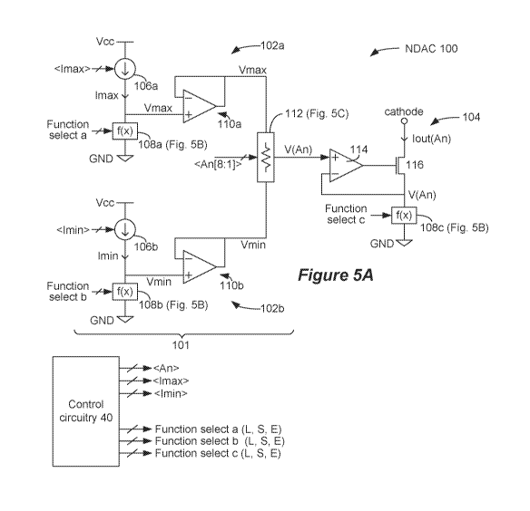
patient requires a lower current such as 1 mA, smaller current adjustments may
result in
meaningful changes to therapy. It may therefore instead be desirable to adjust
the current
with a lower resolution of say 3% (an increment of 0.03 mA), such that
incrementing the
amplitude will increase the current to 1.03 mA, and decrementing the amplitude
will decrease
the current to 0.97 mA. Provider a finer resolution at lower currents would
allow the
clinician (via a clinician programmer) or patient (via a patient remote
controller) to more
flexibility to adjust the current to arrive at a suitable therapy.
[0045] For
patients or therapies requiring higher currents, a constant current
increment of 0.1 mA may be too fine to meaningfully adjust the current. This
increment
works only a 1% resolution to a higher current magnitude of 10 mA (0.1 mA / 10
mA), such
that incrementing the amplitude will increase the current to 10.1 mA, and
decrementing the
amplitude will decrease the current to 9.9 mA. This may comprise too small of
a change
when higher currents are required, because such increments may not
meaningfully affect
therapy. In this circumstance, it might be desirable to the adjust current
with a higher
resolution of (again) say 3% (an increment of 0.3 mA), such that incrementing
the amplitude
will increase the current more significantly to 10.3 mA, and decrementing the
amplitude will
more-significantly decrease the current to 9.7 mA.
16
CA 03167019 2022-07-06
WO 2021/178207
PCT/US2021/019641
[0046]
Designing DAC circuitry such as that shown in Figure 4 that is able to handle
stimulation at lower and higher currents can thus involve undesirable trade
offs. If the DAC
circuitry is designed to provide a good resolution (e.g., 3%) for higher
currents (e.g., 10 mA),
a current increment of 0.3 mA is required. But this would provide an
unsuitably high
resolution (e.g., 30%) at lower currents (1 mA), and adjustments that are too
coarse. By
contrast, if the DAC circuitry is designed to provide a good resolution (e.g.,
3%) for lower
currents (e.g., 1 mA), a current increment of 0.03mA is required. Not only
would this result
in an undesirably low resolution (0.3%) at higher currents (e.g., 10 mA), it
would complicate
DAC circuitry design. If it is assumed for example that the DAC circuitry
should have a
dynamic range of 25.5 mA, a current increment of 0.03 would require the
amplitude to be
controllable in 850 increments (25.5 mA / 0.03 mA). Given the binary nature of
the PDACs
and NDACs (Fig. 4), the digital amplitude bus would now require additional
signals, e.g., ten
signals instead of eight, to properly form the currents. (Ten signal provides
allows 210 = 1024
different amplitudes to be specified by the digital amplitude bus, enough to
handle the 850
required). This complicates DAC design, and may result in values for the
amplitude bus
(those from 851 to 1024) that are invalid.
[0047] Another
shortcoming relating to the DAC circuity having a constant current
increment is that it may be unnecessary for a given application to use its
full dynamic range.
For example, suppose it is known that a given SCS patient requires currents on
the order of 4
mA to provide effective therapy for their symptoms. It may never be warranted
that the
current magnitude for this patient be lower than 3 mA, or higher than 5 mA,
such that the
effective range of the DAC circuitry is from 3 mA to 5 mA for this patient. In
this example,
much of the dynamic range of the DAC circuitry (A<3 mA; 5<A<25.5 mA) is
effectively
wasted on this patient. Further, because the current increment is constant
(e.g., 0.1 mA)
across all amplitude values, the patient can effectively only adjust the
current to 21 of 256
possible amplitude values (e.g. from 3.0 mA to 5.0 mA), which is limiting. It
may be
desirable to allow the patient the adjust the output current more finely
within an effective
range for their needs.
[0048] In
short, DAC circuitry such as that described earlier may be too inflexible. It
is desirable instead to provide a DAC circuitry design that can more
meaningfully increment
and decrement the current depending on the magnitude of that current. For
example, at lower
magnitudes (e.g., 1 mA), the current increment should be lower (e.g., 0.03
mA), while at
higher magnitudes (e.g., 10 mA), the current increment should be higher (e.g.,
0.3 mA). In
17
CA 03167019 2022-07-06
WO 2021/178207
PCT/US2021/019641
short, a design that provides a constant, or at least more constant,
resolution over the dynamic
range is desired.
[0049] Further,
it is desirable to provide a DAC circuitry design that allows the
dynamic range to be set for particular patients or applications, while still
preserving the
ability to finely increment the current over a full range of amplitude values
within that range.
[0050] Finally,
it is desirable to be able to select within the DAC circuitry the use of
different circuits with different current-to-voltage (I-V) characteristics to
control the shape of
the output current. This is because, as explained below, different I-V
characteristics will
have different effects on the manner in which the output current is
incremented, and hence
the resolution of current adjustment, over the dynamic range.
[0051] In
support of these goals, a more-flexible DAC circuitry design 100 is
disclosed starting with Figure 5A. More particularly, Figure 5A shows a new
NDAC
circuitry design which can sink an output current Tout from a cathode. Figures
7A and 7B
later describe alterations to the circuitry to form a PDAC 100 which can
source an output
current Tout to an anode. The new DAC circuitry design can be present as part
of stimulation
circuitry in an IPG or in similar devices, such as an ETS device as described
earlier.
[0052] As
shown, the NDAC circuitry 100 receives a digital amplitude bus <An> and
produces an analog output current, Tout, which is a function of the prescribed
amplitude, An,
carried by the bus. However, as described further below, and depending on how
the NDAC
100 is programmed, the output current Tout may not necessarily linearly scale
with the
amplitude An. That is, Tout(An) may not be incrementable in constant current
increments
(such as Iref) as An is incremented, and thus Tout may not necessarily be
linearly proportional
to A, as occurred in the DAC circuitry described in the Introduction. The
digital amplitude
bus <An> is shown as a parallel bus comprising a plurality of signal lines
(e.g., eight signal
lines An[8] ¨ An[11), but could also comprise a serial bus comprising a single
signal line as
well.
[0053] The NDAC
100 as shown in Figure 5A includes an input stage 101 and an
output stage 104. The input stage in this example includes two biasing stages
102a and
102b. These biasing stages 102a/b can be similar in design, and are used to
set the maximum
(Imax) and minimum (Imin) values for the current that will be produced at the
output, Tout.
Each biasing stage 102a/b includes a current source 106a/b which is
programmable to
produce Imax/Imin. In this regard, the IPG's control circuitry 40 can issue
digital buses
<Imax> and <Imin> as necessary to program the current sources 106a/b to
produce Imax and
Imin. As with other digital buses, these buses <Imax> and <Imin> may comprise
parallel or
18
CA 03167019 2022-07-06
WO 2021/178207
PCT/US2021/019641
serial buses. Note that the current sources 106a/b can comprise any design for
a
programmable current source. For example, current sources 106a/b may be built
as shown
earlier in Figure 4, or can comprise other designs such as those disclosed in
USPs 6,181,969,
8,606,362, 8,620,436, and U.S. Patent Application Publications 2018/0071520
and
2019/0083796.
[0054] The
maximum and minimum currents Imax and Imin are in this example
provided to current-voltage (I-V) selection blocks 108a and 108b (generally
108i), which is
shown in further detail in Figure 5B. I-V selection block 108i allows
different circuits 109i
to be selected to receive Imax and Imin produced by the current sources
106a/b. Preferably,
each of the different circuits 109i has a different current-to-voltage (I-V)
characteristic, and
three different circuits 109i are shown in Figure 5B. The three illustrated
circuits 109i in this
example comprise single devices, although this is just for simplicity. In
other examples the
circuits 109i could comprise one or more devices, i.e., a network of devices,
that together
provide a desired I-V characteristic.
[0055] A first
of the circuits 109L comprises a resistor, whose current IL is linearly
proportional to the voltage across it: IL ¨ kV, where k equals the conductance
of the resistor
(1/R). A second of the circuits 109S comprises a MOS diode, which can be
formed as shown
by connecting the drain of a MOS transistor to its gate. As is known, the
current flowing
through this MOS diode, IS, is proportional to the square of the voltage
across it: IS k(V-
VO2 , where k is a constant, and Vt comprises the threshold voltage of the MOS
transistor. A
third of the circuits 109E comprises a p-n diode, which can be formed in one
example by
connecting the collector of a bipolar junction transistor to its base. As is
known, the current
flowing through this p-n diode, IE, is exponentially proportional to voltage V
across it: IE ¨
m * el", where m and n are constants.
[0056] Any of
these circuits 109L, 109S, and 109E can be selected for use within the
I-V selection blocks 108i by closing switches 111L, 111S, 111E in series with
each. These
switches are respectively controlled by control signals L (linear), S
(square), and E
(exponential), which together comprise function select signals. These function
select signals
are issued by the control circuitry 40, and in the example shown, different
function select
signals a, b, and c are used to control the selection of the circuit 109i in I-
V selection block
108a, I-V selection block 108b, and a third I-V selection block 108c appearing
in the output
stage 104, which will be discussed later. Preferably, but not necessarily, the
control circuitry
40 would select the same circuit 109i in each of the I-V selection blocks
108a, 108b, and
108c. In this regard, and although not shown, the control circuity 40 may
issue only one set
19
CA 03167019 2022-07-06
WO 2021/178207
PCT/US2021/019641
of function control signals¨i.e., one set of L, S, and E control signals¨which
would be
received by each of the I-V selection blocks 108a, 108b, and 108c.
[0057] In
biasing stage 102a, Imax is provided to the selected circuit 109i within I-V
selection block 108a, which in turn produces a voltage Vmax as governed by the
I-V
characteristics of the selected circuit. For example, if resistor 109L is
selected, Vmax will
equal Imax * R. If MOS diode 109S is selected, Vmax would be proportional to
SORT(Imax). If p-n diode 109E is selected, Vmax would be proportional to the
ln(Imax).
Vmax is provided to a voltage follower 110a to produce a buffered version of
Vmax at its
output. Biasing stage 102b is similar, with Imin provided to the selected
circuit 109i within I-
V selection block 108b, which in turn produces a voltage Vmin as governed by
the I-V
characteristics of the selected circuit. Vmin is provided to a voltage
follower 110b to produce
a buffered version of Vmin at its output.
[0058] Vmax and
Vmin as buffered are provided to a resistance block 112 in the
input stage 101, which is controlled by the digital amplitude bus <An> to
produce a voltage
V(An) that varies with the amplitude value An carried by the bus. An example
of resistance
block 112 is shown in further detail in Figure 5C, and includes a
demultiplexer (demux) 120
and a resistor ladder 122. This example assumes that digital amplitude bus
<An> comprises
eight control signals An[8] ¨ An[1] and is thus capable of specifying 256
different amplitude
values. The denum 120 asserts one of 256 possible X control signals in
accordance with the
value of An, as shown in the table in Figure 5C. For example, if An = 0 (<An>
=
'00000000), then denum 120 asserts signal XO; if An = 1 (<An> = '00000001),
then denum
asserts signal Xl, and so on, with X255 asserted when An = 255 (<An> =
'11111111').
[0059] Except
for the case where An = 0 (discussed further below), the asserted X
control signal closes a switch 124 in the resistor ladder 122 to set a value
for V(An) that
equals, or is between, Vmax and Vmin. The resistor ladder 122 includes a
series connection
of 254 resistors in this example, preferably all having the same value, r.
Given the manner in
which the switches 124 are connected to the resistors, voltage V(An) = [(An-
1)/254]*[Vmax-
Vmin] + Vmin. Thus, when An = 1, X1 is asserted, which sets V(An) = Vmin. When
An =
255, X255 is asserted), which sets V(An) = Vmax. V(An) scales linearly between
Vmin and
Vmax for other values of An.
[0060] It may
be desirable to reserve an amplitude that specifies that the NDAC 100
should provide no output, i.e., that lout should equal zero (as opposed to
Imin). This
circumstance is reserved in the depicted example for when An = 0 (<An> =
'00000000'). In
this instance, the denum 120 asserts signal XO, which controls a switch 126
that connects
CA 03167019 2022-07-06
WO 2021/178207
PCT/US2021/019641
V(An) to ground. This sets V(An) to zero, which in turn will set Tout to zero,
as explained
shortly.
[0061]
Referring again to Figure 5A, V(An) is provided to the output stage 104 of the
NDAC 100. Specifically, V(An) is provided to a non-inverting input of an
operational
amplifier (op amp) 114, whose output is provided to the gate of an output
transistor 116. The
inverting input of the op amp 114 is connected to the top of I-V selection
block 108c.
Feedback will force the output transistor 116 on to an extent necessary to
cause the voltages
at the op amp's inputs to be the same; hence V(An) will be dropped across I-V
selection
block 108c. This voltage drop V(An) induces a current Tout through the I-V
selection block
108c and the output transistor 116 in accordance with the I-V characteristics
of the circuit
109i (Fig. 5B) selected in block 108c.
[0062]
Operation of the NDAC 100, and relevance of selecting different of the
circuits 109i, is explained with reference to Figure 5A and Figures 6A-6D. In
the illustrated
examples, it is assumed that Imax is set (via <Imax>) to 25.5 mA, and Imin is
set (via <Imin>
to 0.1 mA. As noted earlier, it is preferred that the circuit 109i selected in
each of the I-V
selection blocks 108a-c be the same, and Figures 6A-6D show the examples where
the
resistors 109L, the MOS diodes 109S, and the p-n diodes 109E are selected in
each block, via
control signals L, S, and E respectively.
[0063] Each of
the selectable circuits 109i in the I-V selection blocks 108i provides a
different scaling to the current Tout as amplitude value An is changed. In
other words, the
selected circuit 109i changes the shape of Iout(An).
[0064] For
example, selection of resistors 109L provides a linear response to Tout as a
function of amplitude An. This results because V(An) produced by the
resistance block 112
will equal V(An) = [R(An-1)/254]*[Imax-Imin] + R*Imin, where R equals the
resistance of
the resistors 109L. When V(An) is impressed across a resistor R in I-V
selection block 108c
in the output stage 104, a current Tout = RAn-1)/2541*[Imax-Imin] + Imin
results. In other
words, Tout is linearly proportional with the amplitude An, as best shown in
Figure 6A.
Notice that Tout ranges from Imin = 0.1 mA (An =1) to Imax = 25.5 mA (An =
255), except
when An = 0, which causes V(A) to be zero, which sets Tout to zero.
[0065] The
selection of MOS diodes 109S provides a squared or parabolic response to
Tout as a function of amplitude An. This results because V(An) produced by the
resistance
block 112 will be proportional to [(An-1)/254]*[SQRT(Imax)- SQRT(Imin)] +
SQRT(Imin),
as dictated by the I-V characteristics for the MOS diodes 109S. V(An) is
impressed across a
MOS diode 109S in the I-V selection block 108c in the output stage 104, which
results in a
21
CA 03167019 2022-07-06
WO 2021/178207
PCT/US2021/019641
current Tout that is generally proportional to An2. The mathematics here are
more
complicated, and may be further complicated by other secondary effects
inherent in a MOS
diode's I-V characteristics (such as consideration of its threshold voltage).
Nonetheless, Tout
generally varies proportionally with An2, as Figures 6A and 6B show. Again,
Tout ranges
from Imin = 0.1 mA (An =1) to Imax = 25.5 mA (An = 255) (except when An = 0,
which sets
Tout to zero).
[0066] The
selection of p-n diodes 109E provides an exponential response to Tout as a
function of amplitude An. This results because V(An) produced by the
resistance block 112
will be proportional to [(An-1)/254111n(Imax)-1n(Imin)] + ln(Imin), as
dictated by the I-V
characteristics for the p-n diodes 109S. V(An) is impressed across a p-n diode
109E in the I-
V selection block 108c in the output stage 104, which results in a current
Tout results which is
proportional to Imin * (Imax/Imin)^((An-1)/254)). In other words, Tout is
exponentially
proportional with amplitude An. This is best shown in Figure 6B, which plots
the logarithm
of Tout versus An. Again, Tout ranges from Imin = 0.1 mA (An =1) to Imax =
25.5 mA (An =
255) (except when An = 0, which sets Tout to zero).
[0067] Figure
6C shows the amount that the output current Tout is incremented when
An is incremented. Mathematically, this graph effectively shows the derivative
d(Iout)/dAn
of the curves provided in Figures 6A and 6B.
[0068] When a
resistor 109L is selected, each increment in the amplitude An provides
a constant increment to the output current Tout, which in this example equals
0.1 mA. (Note
that this makes sense from a calculus standpoint: because Tout varies linearly
with A when a
resistor is used, d(Iout)/dAn should be constant). This response is similar to
the stimulation
circuitry described earlier (Fig. 4), which also provides a constant current
increment (Iref),
and thus an output current that scales linearly with amplitude (Tout = Iref *
An). This may be
fine for a given implementation, but as noted earlier, having DAC that only
allows the output
current to be adjusted in constant increments has drawbacks: the increment may
be too large
to provide good resolution at lower magnitudes for Tout, and too small to
provide good
resolution at higher magnitudes. This resolution (increment/Tout) is
quantified in Figure 6D.
It can be seen that when a constant increment is used (selection of the
resistors 109L), the
resulting resolution is inversely proportional to A. For example, when An =
10,
corresponding to Tout = 1 mA, the resolution is 10% (0.1mA/1mA), and is higher
at even
lower values of An. When An = 100, corresponding to Tout = 10 mA, the
resolution is 1%
(0.1mA/10mA), and is lower at even higher values of An. As discussed earlier,
this
resolution may be too high at lower currents, which inhibits the ability to
make finer
22
CA 03167019 2022-07-06
WO 2021/178207
PCT/US2021/019641
adjustments to the current as might be required for a patient's therapy.
Likewise, the
resolution may be too low at higher currents, resulting in incremental changes
to the current
that are insignificant.
[0069] In this
regard, the selection of non-linear circuits 109i to set the shape of the
output current Tout can be useful, because such circuits provide smaller
increments of current
at lower magnitudes of Tout, and higher increments at higher magnitudes. This
provides a
resolution that is constant, or at least more constant, over the dynamic range
of the NDAC
100.
[0070] For
example, Figure 6C shows that when a MOS diode 109S is selected, the
increment scales essentially linearly with An. (Again, note that this makes
sense: because
Tout is generally proportional with An2, d(Iout)/dAn should generally vary
proportionally
with An). At lower values for the current, the current increment is less than
0.1 mA, and is
approximately 0.1 mA midway through the dynamic range of the NDAC 100 (at An ¨
127).
The increment increases at higher values for An, eventually reaching
approximately 0.2 mA
at Amax = 255. Figure 6D shows the resolution that results from the use of
this non-constant
increment, which is generally between 1 to 8 % over the entire dynamic range
of the NDAC
100. Notice that the resolution may not follow a simple trend due to secondary
effect
inherent in the I-V characteristics in MOS diodes. Nonetheless, when a MOS
diode 109S is
used, and when compared to use of a resistor 109L, the resolution is more
reasonable over the
entire dynamic range of NDAC 100, with smaller resolutions at lower currents,
and higher
resolutions at higher currents.
[0071] When a p-
n diode 109E is selected, the increment varies exponentially with A,
as shown in Figure 6C. (Again, this makes sense: because Tout varies
proportionally with
eAn, d(Iout)/dAn should also vary proportionally with eAn). Because Tout also
varies
exponentially with An, the resulting resolution (Fig. 6D) is constant,
approximately 2.2% in
this example. In other words, each incremental amplitude adjustment to the
output current
raises or lowers Tout by 2.2%. If for example Tout = 1 mA when An =100 (Fig.
6B), then Tout
will equal 1.022 mA when An is incremented to 101. If Tout = 10 mA when An =
215, then
Tout will equal 10.22 mA when An is incremented to 216, etc. Notice that use
of a non-linear
increment in this example solves the problem highlighted earlier, because the
resolution is
constant (e.g., 2.2 %) over the entire dynamic range of the stimulation
circuitry.
[0072] The NDAC
100 is beneficial in its ability to account for variations that might
be present, and thus will perform predictably even in the presence of such
variations. For
example, there may be variations inherent in the manufacturing process used to
fabricate the
23
CA 03167019 2022-07-06
WO 2021/178207
PCT/US2021/019641
NDAC 100, on an ASIC for example, which may change the I-V characteristics of
the
circuits 109i. Further, and particularly as concerns use of MOS diodes 109S or
p-n diodes
109E, the I-V characteristics may depend on temperature. Such variations would
ultimately
affect the voltages Vmax and Vmin that are produced by I-V selection blocks
108a and 108b.
However, because these voltages Vmax and Vmin are subtracted in the resistance
block 112
when forming V(An), and because V(An) is applied to a circuit 109i in I-V
selection block
108c equally affected by such variations, such variations are removed or
mitigated, thus
resulting in values for lout that are predictable.
[0073] Although
it is preferred that the same circuit 109i be selected in each of the I-
V selection blocks 108i, different circuits 109i could be selected. As one
skilled will
appreciate, the use of different types of circuits would create different
shapes for lout as a
function of amplitude (Fig. 6A and 6B), hence providing different lout current
increments
(Fig. 6C) and resolutions (Fig. 6D) throughout the dynamic range of the DAC.
For example,
biasing stages 102a and 102b could be controlled to select use of p-n diodes
109E while
output stage 104 is controlled to select use of a resistor 109L, which might
be beneficial in a
given implementation.
[0074] Figures
7A and 7B shows an example of PDAC 100 able to source a current
lout from an anode, and as one skilled will appreciate, the circuitry is
largely similar to that
of the NDAC 100, and functions similarly. A digital amplitude bus <Ap> is
received, which
forms a voltage V(Ap) that forms a sourced current lout, which can vary
linearly, squarely,
exponentially with Ap depending on the circuits 109i selected. The devices
used in PDAC
100 may have different polarities. For example, P-channel or NPN transistors
can be used
instead of N-channel or PNP transistors used in NDAC 100. Furthermore, digital
control
signals (e.g., <Imax>, <Inain>, <Ap>, function select signals L, S, and E,
etc.) may also be
complementary (active low). Still further, and as explained in U.S. Patent
Application
Publications 2018/0071520, the NDAC 100 and PDAC 100 can be powered by
different
power supply domains. For example, while the NDAC can be powered using power
supply
domain Vcc/GND as shown in Figures 5A and 5B, the PDAC can be powered using
power
supply domain VHNH-Vcc as shown in Figures 7A and 7B.
[0075] Many
modifications to the disclosed DAC circuitry are possible, and some
different examples of modifications are shown in Figures 8-10. Figure 8 shows
an NDAC
100' and PDAC 100', which includes the NDAC 100 and PDAC 100 as described, but
which
include additional amplification stages 110n and 110p. For example, NDAC 100'
includes
NDAC 100, which as described earlier receives amplitude An (via bus <An>),
maximum and
24
CA 03167019 2022-07-06
WO 2021/178207
PCT/US2021/019641
minimum currents Imax and Imin (via buses <Imin> and <Imax>), and function
select signals
(L, S, E) to select a circuit 109i with desired I-V characteristics. NDAC 100
as before
outputs a current Tout between Imin and Imax that varies as a function of An
(either linearly,
squarely, or exponentially). This output current is then provided to an
amplification stage
110n, which (in this example) linearly amplifies Tout by a scalar Jn to
produce an output
current IJ = Jn * Tout at a cathode between Jn * Imin and Jn * Imax. In the
example shown,
scalar Jn is programmable via an amplification bus <Jn> (providable by control
circuitry 40),
but the amplification stage 110n may also provide a fixed amplification of Jn
and not be
programmable. Amplification stage 110n can employ current mirrors to provide
the desired
scalar Jn, and may be built as shown earlier in Figure 4 for example. PDAC
100' is built
similarly, and operates similarly to source a current IJ = Jp * Tout at an
anode.
[0076] The
modification of Figure 9 shows use of DAC circuitry that has only a
single maximum-current biasing stage 102a in the input stage 101. This
example is
illustrated in the context of a NDAC 100, but PDAC 100 (Fig. 7A) could be
similarly
modified. Biasing stage 102a as before is programmed to produce Imax, and in
turn produce
Vmax which is provided to the resistor block 112. When compared with Figure
5A, notice
that minimum-current biasing stage 102b is absent, and instead the other end
of the resistor
block 112 is grounded. This is equivalent to setting Imin = Vmin = 0 in
biasing stage 102b.
In effect then, this modification provides an output current Tout that equals
or ranges between
zero and Imax, which can be useful in applications where it is desirable to
extend the
dynamic range of currents producible by the NDAC 100 down to zero. The same
effect can
be achieved by setting Imax = 0 in biasing stage 102b in Figure 5A. Notice
that control
circuity 40 would not issue <Imin> and function select signals b (L, S, E) in
this example, as
these signals would be irrelevant when biasing stage 102b is lacking.
[0077] Figure
10 shows that the DAC circuitry may not have different selectable
circuits 109i with different I-V characteristics. This example is again
illustrated in the
context of a NDAC 100, but PDAC 100 (Fig. 7A) could be similarly modified. In
Figure 10,
the NDAC 100 include a single non-selectable circuit 109i having a I-V
characteristics
necessary to provide the desired response in Tout as the amplitude is varied.
Specifically,
Figure 10 shows the use of p-n diodes 109E in the DAC (i.e., in place of I-V
selection stages
108i), although other circuits (resistor 109L, MOS diode 109S) could have been
illustrated as
well. Use of a single non-selectable circuit 109i reduces DAC flexibility in
selecting how
Tout will vary with amplitude, but limiting such flexibility can still be a
reasonable design
choice. For example, use of p-n diodes 109E are a reasonable choice if an
exponential
CA 03167019 2022-07-06
WO 2021/178207
PCT/US2021/019641
relationship between Tout and amplitude is desired to produce a constant
resolution over the
entire dynamic range of the DAC (Fig. 6D). Further, although not shown, the
non-selectable
circuits could differ in stages 102a, 102b, and 104. Notice that control
circuity 40 would not
issue function select signals in this example, as these signals would be
irrelevant.
[0078] The
disclosed DAC circuitry is further advantageous in its ability to constrain
the dynamic range of the output current Tout between minimum and maximum
values, Imax
and Imin, which can be useful in in a given application. Take for example the
hypothetical
posed earlier of an SCS patient that requires currents on the order of 4 mA.
As noted earlier,
it may never be warranted that the current magnitude for this patient be lower
than 3 mA, or
higher than 5 mA. In DAC circuitry having a fixed increment (e.g., 0.1 mA),
the patient is
effectively limited to small number of amplitude adjustments within this
dynamic range, such
as 21 out of 256 possible values.
[0079] This
limitation is not present in the current DAC design, and instead the
amplitude can still be varied in 256 increments within the desired dynamic
range, thus
providing the patient more flexibility in adjusting the current within this
range. This is shown
in Figures 11A-11C. In this example, Imin and Imax are programmed (via buses
<Imin> and
<Imax>) to 3 mA and 5mA respectively to provide the desired effective dynamic
range. A
type of circuit 109i¨i.e., resistor 109L, MOS diode 109S, or p-n diode 190E¨is
chosen to
provide a desired relationship between Tout and amplitude An, as explained
earlier. Notice
that constraining the dynamic range of Tout can flatten the responses as shown
in Figure 11A,
although these responses are still linear (resistor 109L), squared (MOS diode
190S) and
exponential (p-n diode 190E) as described earlier. Figure 11B and 11C show the
resulting
increments and resolutions as a function of amplitude An, which show the same
basic
responses noted earlier (although again flattened). As shown in Figure 11B,
the current
increment in Tout is constant (¨ 0.0078 mA) when resistor 109L is used;
generally linearly
increasing when MOS diode 109S is used; and exponentially increasing when p-n
diode 109E
is used. As shown in Figure 11C, the resolution inversely decreases when
resistor 109L is
used, and is constant (¨ 0.2%) when p-n diode 109E is used. (The resolution
for the MOS
diode 109S is not shown in Figure 11C for simplicity).
[0080] Figures
12A and 12B shows the integration of the disclosed NDAC 100 and
PDAC 100 in a stimulation circuitry 128 used to provide currents to an IPG's
electrodes.
These stimulation circuitries 128 are similar to the stimulation circuitries
shown earlier in
Figures 3A and 3B, and show examples in which PDACi/NDACi pairs are dedicated
to
particular electrode nodes ei (Fig. 12A), and in which PDACs and NDACs can
control the
26
CA 03167019 2022-07-06
WO 2021/178207
PCT/US2021/019641
current at different electrodes through switch matrices SM Pi and SM Ni (Fig.
12B). Further
shown are the control signals received by the various components, which as
noted earlier can
issue from the IPG's control circuitry 40. In the examples shown, each PDACi
and NDACi
receives a digital amplitude bus <Api> and <Ani>. Each PDACi and NDACi can
further
receive control signals unique to the disclosed DAC design, such as those to
set the maximum
and minimum currents (<Imaxpi>, <Iminpi>, <Imaxni>, <Iminni>), and the
function select
signals (L, S, E(pi), and L, S, E(ni)) used to shape Tout. In one example, the
maximum and
minimum currents, and the function select signals may be the same for each of
the PDACs
and NDACs. In this regard, the control circuitry 40 may only need to issue,
and each PDACi
and NDACi may receive, one set of such signal (i.e., <Imax>, <Imin>, and L, S,
or E). In
Figure 12B, the switch matrices SM Pi and SW Ni additionally receive switch
matrix control
signals <SPi> and <SNi> as before.
[0081] Figure
13 shows a graphical user interface (GUI 150) that can be used to
program and control operation of the disclosed DAC circuitry. One skilled will
understand
that the GUI 150 can be rendered on the display of an external devices used to
program or
monitor the IPG, such as a hand-held patient remote controller or a clinician
programmer.
The software used to render GUI 150 and to receive inputs from the user can be
stored in a
non-transitory computer-readable medium, such as in memory in the external
device.
[0082] The GUI
150 can include a DAC circuitry control interface 152 that allows
one or more of the PDACs and NDACs to be selected and programmed. In Figure
13, it is
assumed that the IPG's stimulation circuitry 128 includes four PDACs and four
NDACs,
although this number could vary depending on the design of the stimulation
circuitry. DAC
programming can include options to specify the maximum and minimum currents to
be
produced by the relevant DAC(s), Imax and Imin, and options to select the
shape of the Tout
versus amplitude, such as linearly, squarely, or exponentially, which would
respectively
select the use of resistors 109L, MOS diodes 109S, and p-n diodes 109E in the
stimulation
circuitry 128. Such programming can be transmitted from the external device to
the IPG to
allow the IPG's control circuitry 40 to form buses <Imax>, <Imin>, and the
function select
signals L, S, and E for each or all of the DACs. (In other DAC designs, <Imin>
and the
function select signals may not be relevant (see Figs. 9 and 10), in which
case control for
such variables could be omitted from the GUI 150).
[0083] Because
the external device can be programmed with the relevant I-V
characteristics of the circuits 109i used in the DAC circuitry, the external
device can compute
the current Tout corresponding to each amplitude value (Iout(A)) given Imin,
Imax, and the
27
CA 03167019 2022-07-06
WO 2021/178207
PCT/US2021/019641
selected Tout shape. In effect, the external device can determine the data
necessary to form
the graphs shown earlier in Figure 6A, which shows Tout versus A. If necessary
or useful,
Tout(A) can be displayed in the GUI 150 as a table of values, or it could be
graphed as in
Figure 6A. From the Tout(A) data, the external device can further determine
the increment
and the resolution, or ranges for both, as described previously. In effect,
the external device
can determine the data necessary to form the graphs shown earlier in Figures
6C and 6D, and
such data may again be graphed. The displaying of such information in GUI 150
can be
useful to review, and can aid the user in the selection of a proper Tout shape
given Imin and
Imax. For example, the user can review the resolution provided over the
dynamic range of
selectable amplitudes to ensure that each amplitude increment will provide a
significant
adjustment to Tout.
[0084]
Establishing Tout(A) in the external device can also be useful to enable the
external device to convert desired currents magnitudes into amplitude values A
that will be
carried by the digital amplitude buses (<Ap>, <An>) in the DACs. In this
regard, GUI 150
can include an electrode programming interface 154 that allows a user (patient
or clinician) to
specify currents I to be produced at each of the electrodes in the IPG
electrode array 17. In
an actual implementation, the electrode programming interface 154 could be
significantly
more complicated and could include additional options to specify the
stimulation that the
patient will receive. For example, frequency and pulse width of the pulses
could also be
specified, but this isn't shown for simplicity.
[0085] In the
example shown, the user has selected electrodes El and E3 to act as
anodes, with each sourcing +2.0 mA to the patient's tissue. The user has also
selected
electrode E2 to act as a cathode to sink -4.0 mA from the patient's tissue.
Knowing how Tout
scales with amplitude (Iout(A)) for the selected Tout shape, the external
device can determine
an amplitude value A needed to establish a desired current I, and this can
occur using an
amplitude conversion module 130 stored in the external device in association
with the GUI
150's software. Assume for example that the stimulation circuitry 128
architecture of Figure
12A is used (with each electrode Ei having a dedicated PDACi/NDACi pair), and
that the
user has programmed the DACs to provide an exponential response to Tout. As
noted above,
the external device can determine Iout(A), and provide this to the amplitude
conversion
module 130 so that amplitude values A can be determined for each of the
specified currents I.
Referring to the graph of Tout v. A in Figure 6C when an exponential shape is
selected, we
can see that currents of 2 mA and 4 mA correspond to amplitude values of 138
and 170
respectively. As such, the amplitude conversion module can set digital
amplitude bus <Apl>
28
CA 03167019 2022-07-06
WO 2021/178207
PCT/US2021/019641
(servicing PDAC1 and electrode El) to 138 ('01110101', 138 active low),
digital amplitude
bus <An2> (servicing NDAC2 and electrode E2) to 170 ('10101010', 170 active
high), and
digital amplitude bus <Ap3> (servicing PDAC3 and electrode E3) to 138
(01110101', 138
active low). These amplitude values can then be transmitted from the external
device to the
IPG along with the other relevant data to allow the control circuitry 40 in
the IPG to form the
control signals necessary for the stimulation circuitry 128 to form the
desired stimulation.
[0086]
Alternatively, the external device can transmit the desired current magnitudes
to the IPG 10, leaving it to the IPG 10 to convert these currents to amplitude
values. In this
regard, the IPG's control circuitry 40 can also include an amplitude
conversion module 130,
as shown in Figures 12A and 12B. Thus, the control circuitry 40 in the IPG 10
can determine
Iout(A) given the other user selections in the GUI 150 (Imin, Imax, Tout
shape, etc.), or
Iout(A) can also be telemetered to the IPG. In either case, the module 130 can
determine the
amplitude values A necessary to form the desired currents I at each of the
electrodes.
29