Note: Descriptions are shown in the official language in which they were submitted.
WO 2021/163229
PCT/US2021/017513
APPARATUSES AND METHODS FOR WIRELESSLY POWERED CHARGE-
BALANCED ELECTRICAL STIMULATION
[0001] This Patent Application claims priority to U.S. Provisional
Patent
Application Serial No. 62/972,639, filed February 10, 2020, the content of
which
is hereby incorporated by reference herein in its entirety into this
disclosure.
BACKGROUND OF THE SUBJECT DISCLOSURE
Field of the Subject Disclosure
[0002] The present subject disclosure relates to systems and methods
for
efficient wireless powering and control of an electrical load.
Background of the Subject Disclosure
[0003] Neurostimulators are a class of implantable medical devices
which have
achieved successful clinical implementation in the past several decades. In
general, they provide voltage or current pulses to electrically activate
tissue in
order to stimulate or suppress nerve function. Among the achievements of this
technology are restoring sensory function to patients with damaged hearing,
reducing the severity of tremors, treating depression, and rehabilitating
voluntary
motion of muscles and sphincters, among others. Almost all of these devices
require implantation in a miniaturized, hermetic, and biocompatible enclosure
in
order to fit into the limited space available in the surroundings of the brain
or the
target nerve tissue. Given the importance and sensitivity of these tissues,
1
CA 03167617 2022- 8- 10
WO 2021/163229
PCT/US2021/017513
neurostimulators operate at very high power efficiency to avoid heat damage.
Another requirement of neurostimulation is charged balanced stimulation.
Neurostimulators provide electrical pulses to neural tissue through
specialized
electrodes. As current crosses the electrode-electrolyte interface, different
kinds
of physical and chemical processes occur. A constant unidirectional current
applied on this interface may eventually cause irreversible chemical processes
that destroy the electrode and generate harmful chemical compounds that result
in tissue damage. This effect also occurs in stimulators that present biphasic
electrical waveforms as stimulus, but with non-zero net charge. Over time,
accumulated charge imbalances can lead to the aforementioned undesirable
effects.
SUMMARY OF THE SUBJECT DISCLOSURE
[0004] Of the conventional neural stimulators available today, retinal
prostheses
are a type that aims to restore vision to blind patients. At this moment,
retinal
prostheses have not had the same clinical success as other stimulators, such
as
cochlear stimulators have in restoring hearing to deaf patients. The retinal
prosthesis strategy generally involves electrical stimulation of the remaining
retinal tissue, in the case of patients with a diseased retinal photoreceptor
cells,
to elicit light perception. There is a direct relationship between the
geometrical
characteristics of retina stimulation and the perceived shape of the perceived
visual image. Thus, retinal prostheses aim to provide as many channels of
stimulation as possible, in order to approximate healthy vision which can
2
CA 03167617 2022- 8- 10
WO 2021/163229
PCT/US2021/017513
perceive high resolution 2D images. This presents a problem to the
requirements
of implantable neurostimulators, as a conventional high channel count
neurostimulator would: generate too much heat through inefficient stimulation
and high data rate video transmission; require very bulky interconnect to
control
so many channels; and cause tissue damage and reduced electrode lifetime due
to charge unbalanced stimulation. The present subject disclosure provides,
among other things, a technical solution to these technical problems.
[0005] A recent approach toward reducing the number of interconnect
channels
while maintaining effective high resolution stimulation was to develop a dual
purpose electrode and photosensor array that could be placed under the retina.
This array of photo-sensors can be globally biased with a voltage pulse using
only two wires, and would produce currents from each electrode proportional to
the amount of incident light on each electrode/pixel. Although there are many
benefits from this approach, powering and controlling this system wirelessly
while
minimizing wasted power, and implant size has not been fully accomplished.
[0006] Despite the advancements in retinal prostheses, there is a need
for a
solution to efficiently power and control optically modulated multichannel
stimulating arrays with minimal interconnect and charge balanced outputs.
BRIEF DESCRIPTION OF THE DRAWINGS
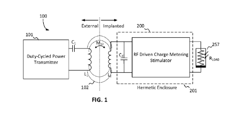
[0007] Fig. 1 shows an RF driven charge metering stimulator driving a
load in an
implant inductively coupled to an external duty-cycled power transmitter,
according to an exemplary embodiment of the present subject disclosure.
3
CA 03167617 2022- 8- 10
WO 2021/163229
PCT/US2021/017513
[0008] Fig. 2 shows an RF driven charge metering stimulator, with power
subsystem, signal receiver and synchronization subsystem, stimulator
subsystem, and data transmitter subsystem, according to an exemplary
embodiment of the present subject disclosure.
[0009] Fig. 3A shows a power subsystem, according to an exemplary
embodiment of the present subject disclosure.
[0010] Fig. 3B shows regions of operation in rectifying and regulating
the AC RF
input into output DC voltages of the power system shown in FIG. 3A, according
to an exemplary embodiment of the present subject disclosure.
[0011] Fig. 4 shows a rectifier in the power subsystem, according to an
exemplary embodiment of the present subject disclosure.
[0012] Fig. 5 shows a dual supply complementary voltage limiting
regulator,
interfacing to the rectifier in the power subsystem, according to an exemplary
embodiment of the present subject disclosure.
[0013] Fig. 6A shows low-ranging (LO) error amplifiers in the voltage
limiting
regulator, according to an exemplary embodiment of the present subject
disclosure.
[0014] Fig. 6B shows high-ranging (HI) error amplifiers in the voltage
limiting
regulator, according to an exemplary embodiment of the present subject
disclosure.
[0015] Fig. 7 shows a signal receiver and synchronization subsystem,
and
example waveforms in the generation of the Pulse and Detect Hold signals from
the RF input, according to an exemplary embodiment of the present subject
4
CA 03167617 2022- 8- 10
WO 2021/163229
PCT/US2021/017513
disclosure.
[0016] Fig. 8 shows a stimulator core subsystem which implements
adiabatic
voltage stimulation and charge metering, according to an exemplary embodiment
of the present subject disclosure.
[0017] Fig. 9 shows a phase logic and switch driver which resets the
metering
capacitor in the stimulator core subsystem, according to an exemplary
embodiment of the present subject disclosure.
[0018] Fig. 10 shows a principle of operation with example timing
diagram of the
adiabatic charge metering stimulator, according to an exemplary embodiment of
the present subject disclosure.
[0019] Fig. 11 shows a regulated supply's voltage invariant current
reference,
according to an exemplary embodiment of the present subject disclosure.
[0020] Fig. 12 shows a complementary high-output-swing cascode bias
generator, according to an exemplary embodiment of the present subject
disclosure.
[0021] Fig. 13 shows a real time comparator using a folded cascode
architecture,
according to an exemplary embodiment of the present subject disclosure.
[0022] Fig. 14 shows an uplink data transmission through load shift
keying by
parallel detuning of the secondary resonator, according to an exemplary
embodiment of the present subject disclosure.
[0023] Fig. 15 shows an uplink-downlink data telemetry arbitration
scheme,
according to an exemplary embodiment of the present subject disclosure.
[0024] Fig. 16 shows a principle of operation with example timing
diagram of the
CA 03167617 2022- 8- 10
WO 2021/163229
PCT/US2021/017513
adiabatic charge metering stimulator with the addition of voltage calibration
phases, according to an exemplary embodiment of the present subject
disclosure.
[0025] Fig. 17 shows a stimulation phase state diagram with transitions
toggled
by downlink telemetry events, according to an exemplary embodiment of the
present subject disclosure.
DETAILED DESCRIPTION OF THE SUBJECT DISCLOSURE
[0026] The present subject disclosure addresses the shortcomings of
conventional retinal prostheses by providing novel apparatuses and methods
which offset the power load to an external component. Thus, the present
subject
disclosure provides, among other things, a technical solution to a technical
problem, as described in detail above and appreciated by one having ordinary
skill in the art.
[0027] The present subject disclosure describes apparatuses and method
for RE
driven charge metering stimulation comprising various components interfacing
to
an inductive coil, electrical load, and optional calibration load including,
for
example: a power subsystem, signal receiver and synchronization subsystem,
stimulator subsystem, and data transmitter subsystem. The power subsystem
comprises a rectifier and a dual supply complementary voltage limiting
regulator
along with specialized supply range extending error amplifiers. The signal
receiver and synchronization subsystem demodulates downlink telemetry signals
and controls the internal state machine. The stimulator subsystem implements
6
CA 03167617 2022- 8- 10
WO 2021/163229
PCT/US2021/017513
adiabatic voltage stimulation to a photosensitive or variable load while at
the
same time metering the delivered charge. Charging and discharging of a series
capacitor is accomplished by a reset switch that responds to the charge
monitoring comparator. The system saves considerable power by being able to
operate at a wide range of supply voltage, thus outsourcing voltage conversion
and computational functions to the external system where inefficiencies of
power
transmission and conversion are not compounded. All circuits including power,
comparator, references and output buffers are thus designed for wide supply
operation. Uplink or backtelemetry data transmission is accomplished by
detuning of the internal resonator connecting a capacitor in parallel for load
shift
keying of discrete charge quanta events with appropriate bidirectional
communication arbitration. The system also provides for additional calibration
phases to a known load, to de-embed the effect of wireless link and load
uncertainty and precisely monitor the receivers available voltage supply.
[0028] Efficiently transmitting power and control data to an
inductively powered
neurostimulator can be accomplished by outsourcing many of the power
intensive tasks out of the implant and into the external power system where
there
is more space to implement energy efficient solutions, and heat from wasted
power does not result in tissue damage. FIG. 1 shows an exemplary embodiment
of the system concept 100, which is a wireless efficient adaptive stimulation
system. A first solution is to create a system that is only powered during the
time
it is required to output a pulse. Therefore a duty cycled transmitter 101 is
used
which powers the device 200 dynamically as needed to produce pulses. This
7
CA 03167617 2022- 8- 10
WO 2021/163229
PCT/US2021/017513
duty cycled power, is not only saving energy during the off-time of the pulse,
but
effectively time encoding the pulse width data into the power signal duty
cycle;
obviating the need to transmit, decode and process this data. The external
duty
cycled power supply 100 is inductively coupled 102 to the implant, which is an
RF driven charge metering stimulator 200. The implant 200 may be full encased
within a hermetic enclosure 201. The stimulator 200 is in turn connected to
the
electrode array and reference ground electrode using only two wires. To the
charge metering stimulator, the electrode array is electrically equivalent to
a
single non-linear photosensitive load impedance, so knowledge of the output
voltage is not sufficient to enforce charge balanced stimulation.
[0029] An overview of the architecture of the RE driven charge metering
stimulator 200 is shown in the block diagram of FIG. 2. The system 200
designed
to exemplify the implanted neurostimulator comprises of 4 major subsystems:
Power 210, Data Receiver and Synchronization 230, Stimulator Core 250, and
Data Transmitter 270. Each of these blocks has been designed with the
principle
of delegating functions to the external system 101 in order to save power. As
the
systems have very different functions, different strategies contribute to
overall
novelty and efficiency.
[0030] Power Subsystem
[0031] In order to control the amplitude of a stimulating pulse, a
stimulator system
can either have a variable power supply rail or make use of digital to analog
converters. Power conversion in conventional neurostimulators, and many other
electronic systems, usually requires the use of DC-DC converters. These
8
CA 03167617 2022- 8- 10
WO 2021/163229
PCT/US2021/017513
converters require large capacitors, and sometimes even larger inductors to
achieve high efficiency. This property makes them undesirable in miniature
implants where space is a significant constraint. Additionally, DC-DC
converters
usually convert a fixed ratio of voltages. Alternatively, variable regulators
or other
digital to analog converters can generate any desired voltage level lower than
a
maximum constant power supply. This second approach is even more wasteful,
as the system maintains a high voltage supply even as it outputs low voltage,
usually completely wasting the difference in power.
[0032] In the system of the subject disclosure, the stimulating output
pulse
amplitude is controlled by the external power system 101. During the duty
cycled
power, the implanted system 200 has an AC-DC converter, or rectifier 211, that
can operate in a broad range of AC voltage amplitude. The received RE energy
is rectified with low losses, and low voltage drops, to produce the system's
unregulated power supply. This unregulated voltage will be directly connected
to
the load avoiding regulators and other intermediate steps and energy costs. By
increasing or decreasing the amplitude of the external transmitter 101 we can
directly control the output voltage of the stimulator 200. The cost of this
energy
savings is that the rectifier 211, and the rest of the system's circuits, must
operate correctly at a wide range of voltage supply levels. So not only does
this
method save energy by avoiding voltage conversion losses, but it also saves
energy by obviating the need for amplitude data transmission, detection and
processing. This power distribution strategy is described in FIG. 3A.
[0033] FIG. 3A shows a power subsystem, and FIG. 3B shows regions of
9
CA 03167617 2022- 8- 10
WO 2021/163229
PCT/US2021/017513
operation in rectifying and regulating the AC RF input into output DC voltages
of
the power system shown in FIG. 3A. For practical implementation of this
system,
not all integrated circuit processes have a wide supply range. Therefore, it
is also
necessary to generate low-power consuming regulated supplies in order to
protect thinner gate transistors required for high speed digital and well
performing
analog circuits. Even though linear regulators were used to limit the analog
and
digital power at the high end of the RF levels, these do not significantly
affect
total system efficiency, as most of the power consumed by the system is taken
from the unregulated supply to drive the load.
[0034] Rectifier
[0035] In order to accomplish the power savings and architecture
simplifications
that result from the aforementioned strategy, the architecture of the
rectifier 211
aims to maximize power conversion efficiency and voltage conversion ratio over
a wide range of input and output conditions. While there exist many
architectures, they are usually optimized for a single load or voltage
condition.
The proposed rectifier manages very low conductive losses by a combination of
fully cross-coupled complementary PMOS and NMOS pairs. Additionally, a
native NMOS, or near-zero threshold device, is inserted to reduce the reverse
current when (VRF+ - VRF-) > 0 but VRF+ < VDD. FIG. 4 shows the architecture
of
an exemplary rectifier. This design improves on an existing method by only
using
one type of native transistor (n-type in this case), eliminating the redundant
reverse current protection which reduces voltage drop, and making the design
possible in a wider array of semiconductor processes that don't have
CA 03167617 2022- 8- 10
WO 2021/163229
PCT/US2021/017513
complementary native devices. The proposed rectifier 211 also has the
advantage to switch itself with the existing RF sinusoid, obviating the need
for
comparators, phase detectors, and phased locked loops usually present in
active-rectifiers. These three mixed signal blocks require significant design
effort,
greatly increase power overhead, and generally must be optimized for a narrow
range of operating voltage and frequency. Therefore, this rectifier presents
significant improvement over previous strategies as it has low power
consumption overhead, and its wide operability can enable external transmitter
control of stimulation amplitude.
[0036] Dual Complementary Regulators
[0037] Many semiconductor processes provide higher-voltage-tolerant
transistors
as well as smaller, faster, standard transistors useful for high performance
analog and digital operations. In this design, both kinds are harnessed to
extend
the functional range. In order to execute the power strategy proposed in FIG.
3B, we require regulation of the main power supply VDD. As the goal is to make
secondary supplies that will not destroy the low-voltage devices, we require a
limited voltage supply with respect to ground VSS, as well as another limited
voltage with respect to VDD. In order to accomplish this we have designed a
dual
complementary low dropout regulator to limit both supply rails.
[0038] The dual regulator architecture, shown in FIG. 5, has 3 main
regions of
operation shown in FIG. 3: cutoff 215, transparent 216, and limiting 217. In
the
Cutoff region 215, the unregulated voltage VDD is too low to power the error
amplifiers that control the pass transistors, thus the regulated supplies are
turned
11
CA 03167617 2022- 8- 10
WO 2021/163229
PCT/US2021/017513
off if VDD is less than VaDc min. In the Transparent region 216, the
regulators turn
on the pass transistor such that the regulated supplies are almost the same
amplitude as the unregulated supplies (except for the dropout voltage across
the
pass transistors). In the Limiting region 217, when VDD exceeds the safe limit
of
the low-voltage transistors, ViDc max Lv the error amplifiers decrease the
conductivity of the NMOS and PMOS pass transistors to maintain VDDLim at VDC
max LV and VDD-VSSum at VDcmaxLv. Finally, a fourth region 218 exists where
overvoltage Protection prevents breakdown of all circuits above VAC max. This
design improves on existing regulator architectures in that the error
amplifiers,
driven by the unregulated supply as a power source, default to complementary
high (HI), and low (LO) voltages when the supply is insufficient to operate
the
amplifier correctly
[0039] One possible architecture for the complementary error amplifiers
is shown
in FIGS. 6A-6B. The use of complementary-defaulting-to-rail architectures is
what enables the operation of the regulator at lower VDD voltages and thus
decreasing VDC min and correspondingly VAcmin. This allows the permissible
output voltage range of the stimulator to span [VDC min , VDC max Ha while
utilizing
the advantages of both high voltage and low voltage transistors.
[0040] Data Subsystem
[0041] The signal receiver and synchronization subsystem consists of a
downlink
telemetry receiver, clock recovery circuit, power-on reset circuit, and system
state machine. Its purpose is to receive data signals from the external
controller,
recover a clock of the same frequency as the carrier wave, and setup the
correct
12
CA 03167617 2022- 8- 10
WO 2021/163229
PCT/US2021/017513
sequence of calibration and stimulation. As part of the strategy to reduce the
amount of operations on the implantable system, the only data transmitted
downlink is a single bit asynchronous, time encoded, amplitude modulated pulse
signaling a change in the stimulation phase. As described previously, the
amplitude of the stimulation waveform and the duration of the stimulation
waveform are analog encoded on the RF signal by the external transmitter, to
minimize power dissipation and operational complexity in the implant.
[0042] Data Receiver
[0043] In order to receive the phase-changing data pulses the amplitude
modulated RF wave is demodulated. In this system we propose a strategy for
demodulation that involves the proposed rectifier 231 shown and described in
FIG. 4 as rectifier 211. The system diagram of the downlink data receiver is
depicted on FIG. 7. As the proposed rectifier 231 is an efficient, wide input
range
circuit, the same architecture can be applied toward demodulating the RF
signal
envelope. In order to minimize power syphoned away from the rectifier system,
this auxiliary rectifier 231 is many times narrower than the primary power
rectifier
211, as it needs to drive a much smaller load. After the signal demodulating
rectifier 231, the signal encounters an integrating capacitor 232 and a
current
sink 233 that permits the demodulated voltage to decrease after the modulated
signal pulse is over. Subsequently a mixed signal active bandpass filter 234
conditions the signal to enhance the pulse. After the bandpass filter 234, a
real
time comparator 235 detects threshold crossing pulses. When a pulse is
detected, a circuit, Pulse Gen 236, generates a digital pulse signal of a
standard
13
CA 03167617 2022- 8- 10
WO 2021/163229
PCT/US2021/017513
duration, while another circuit, Hold Gen 237, generates a much longer hold
signal that digitally resets the bandpass filter and prevents any duplicate
events
from detection for a refractory period.
[0044] Stimulator Subsystem
[0045] FIG. 8 shows an exemplary embodiment of the stimulator subsystem
250.
The stimulator subsystem 250 provides a voltage pulse waveform by directly
connecting the duty-cycled and amplitude modulated supply VDD to the desired
load. To this end, the stimulator subsystem 250 relies on three tri-state
switches,
or Output Buffers 254, that can connect each terminal of either the intended
load
255, or a known calibration resistor 256 to VDD or VSS. As the current flows
through the load RLOAD 257, metering capacitor CMET 258 begins charging until
it
reaches a set differential voltage threshold, at which point the comparator
259
monitoring this voltage activates a reset switch to discharge the capacitor.
Each
time there is a discharge event, an amount of charge 0 = CMET Vthresh.
Therefore
this stimulator 250 outputs an analog voltage of arbitrary amplitude to drive
a
load of unknown impedance while outputting digital counts of the delivered
charge. This method conserves a lot of power, and prevents complexity and
error
in the system compared to a series transimpedance amplifier or series resistor
current measurement. A transimpedance amplifier is impractical as currents of
the order of miliannperes would need to be driven through an operational
amplifier at great cost in headroom power. Similarly, a series resistor
current
measurement would require a precise, linear, high bandwidth amplifier, and an
accurate analog to digital converter to quantize the current followed by
digital
14
CA 03167617 2022- 8- 10
WO 2021/163229
PCT/US2021/017513
integration to calculate total charge. Instead, the proposed system is not
only
simpler and more power efficient, but the charge quantization signals may be
directly used to send backtelemetry events to the external system.
[0046] The switches in the Output Buffers 254 are designed to have very
low
impedance in order to reduce power consumption and voltage drop across them.
They also have to be built to withstand the full range of stimulation voltage,
and
so in this implementation they are designed to use high voltage tolerant 10
transistors. In order to have both low impedance, especially at very low
voltages,
and tolerate high voltages, the switches were sized considerably large in
relation
with the rest of the system. Although the area occupied by the switches is
significant, it is an acceptable trade-off for the large range of operation of
the
stimulator, which is approximately [0.5-3V] in the implemented process, but
may
be significantly higher in processes with higher voltage tolerant devices. The
output buffers 254 are preceded by HV Buffer Drivers 253, output multiplexor
logic 251, and voltage level shifters 252.
[0047] Although the output buffers 254 and corresponding drivers are
implemented with high voltage tolerant devices, the rest of the stimulator 250
is
entirely composed of standard gate thickness low voltage devices, for size
speed, and threshold voltage considerations. In order to operate in
potentially
breakdown inducing conditions, several strategies were taken to protect the
circuits while utilizing the advantages of the standard devices.
[0048] The comparator 259 required to detect whether CmET 258 has
exceeded
the desired threshold voltage is capacitively coupled preventing DC
overvoltage.
CA 03167617 2022- 8- 10
WO 2021/163229
PCT/US2021/017513
This capacitive coupling is also advantageous to apply a differential bias
through
VBN VBP. In this way the comparator 259 acts like an open loop difference
differential amplifier. The comparator also has the capability to perform an
auto-
zero cycle to eliminate intrinsic offsets and set the otherwise-floating input
voltage operating point.
[0049] Another component of the stimulator may be the reset switch RST
260. A
diagram describing these switches and supporting structures is shown in FIG.
9.
An exemplary phase logic metering switch driver is shown in the figure. As
switching is desired to be fast and efficient, low voltage standard devices
are
used. In order to prevent overvoltage at the reset switch, several strategies
are
applied. First the NMOS reset switch is isolated through triple well, and as
usual
the PMOS switch is implemented in its own n-well. Second, the comparator
prevents the source drain voltage from exceeding a set threshold_ Third the
high
speed drivers required to switch the reset switches on and off are powered by
a
muxed power supply. For example, in the positive current phase, if VDD exceeds
VDC max LV, the RSTs NMOS transistor driver is driven with VDDLim. Conversely,
in
the reverse current phase when the switch terminal VDUTN is connected to
VDD, the RSTs PMOS is driven with VSSum as a low supply rail. To make this
possible, logic circuits, a power rail selector mux, and dual rail level
shifters (level
translators) are implemented on the drivers. The drivers are sized for maximum
speed of reset using the principles of logic effort sizing.
[0050] A description of the signals involved in the adiabatic charge
metering
stimulator are represented in FIG. 10. As the unregulated supply voltage VDD
16
CA 03167617 2022- 8- 10
WO 2021/163229
PCT/US2021/017513
charges up to VHI at the beginning of a duty cycled pulse the comparator
undergoes autozero and the state machine is reset. Thereafter, VDD is
connected to the load providing positive VHI of voltage across the load
terminals.
During this time, the metering capacitor charges and discharges as the
comparator input reaches threshold. The voltage excursion of the metering
capacitor causes a triangle ripple voltage across the applied load voltage.
However, considering it is desirable for the reset threshold to be low, and
the
switching frequency to be much higher than the stimulation (pulse repetition)
frequency; it will not affect the performance of this system as a
neurostimulator.
For each charge quantum completed, there is an immediate backtelemetry event
pulse. When the first phase is complete the external system sends an
upmodulated pulse to signal a phase change, and the amplitude of the RF signal
is immediately decreased to change VDD to VL0 . After a brief autozero period,
the stimulator turns on applying a negative VW voltage across the same
terminals mentioned above. Similarly, charge quanta cause resets, which in
turn
are transmitted back to the external system. Enforcing the reverse phase
duration to contain the same number of charge quanta as the first, in other
words
charge balance, can simply be done from the external system.
[0051] FIG. 11 shows the current reference with supply variation
rejection circuit,
and FIG. 12 shows high output swing bias generator circuit, for the real time
comparator 259 in the stimulator 250. The comparator 259 itself is a folded
cascode amplifier designed with reduced threshold devices in order to operate
at
very low voltage. The combination of the design choices for the current and
bias
17
CA 03167617 2022- 8- 10
WO 2021/163229
PCT/US2021/017513
generators, as well as the amplifier enable the extended operating range which
is
a benefit of this design. The architecture of the folded cascode comparator is
shown in FIG. 13.
[0052] Data Transmitter Subsystem
[0053] Finally, the backtelemetry subsystem 270 is responsible for
transmission
of uplink data from the implant 200 to the external transmitter 101. Whereas
downlink data was transmitted through amplitude shift keying (ASK). Uplink
data
is transmitted through load shift keying (LSK). The external and internal
resonators in the system, described in FIG. 1, are coupled in such a way that
changes in the resonance of the implanted resonator (or even an extreme and
sustained rise in power consumption) can be observed on the external system as
a reflected impedance.
[0054] When a charge quanta has been delivered to the load, FIG. 14
shows how
a driver and switch system connects additional capacitors to the resonator in
order to detune the system and send a backtelemetry pulse signal. This figure
shows data transmission strategy vertical. Though higher duration
backtelennetry
pulses and greater magnitude of detuning generate a stronger signal at the
external transmitter, they also consume large amounts of power which may
inadvertently power down the system
[0055] In order to prevent incoming and outgoing events from colliding,
an
uplink/downlink arbitration scheme at the implant is proposed and implemented
as a timed state machine, shown in FIG. 15. An additional, but similar system
may be included in the external system that ensures data is transmitted
faithfully.
18
CA 03167617 2022- 8- 10
WO 2021/163229
PCT/US2021/017513
[0056] A remaining detail in the functionality of the system is worthy
of attention.
The external and internal systems are loosely inductively coupled. As this
implementation details a retina implant application the coil may be tethered
to the
eyeball, changing the coupling coefficient whenever eye movements such as
saccades and microsaccades occur. In order to ascertain the exact value of the
implant's VDD at the time of stimulation, an additional known resistance is
provided as a test load. By connecting this resistor to VDD and monitoring the
number of charge metering pulses, the system transmits to the external system
the information required to calculate VDD. FIG. 16 shows the role of
calibration
on the system and how charge quanta pulses can be used both to enforce
charge balanced stimulation and closed loop voltage control. Having discussed
the reasons and implementation of calibration, FIG. 17 shows the implemented
state machine of the system cycling through calibration and stimulation phases
as downlink phase changing events are sent from the external system.
[0057] The foregoing disclosure of the exemplary embodiments of the
present
subject disclosure has been presented for purposes of illustration and
description. It is not intended to be exhaustive or to limit the subject
disclosure to
the precise forms disclosed. Many variations and modifications of the
embodiments described herein will be apparent to one of ordinary skill in the
art
in light of the above disclosure. The scope of the subject disclosure is to be
defined only by the claims appended hereto, and by their equivalents.
[0058] Further, in describing representative embodiments of the present
subject
disclosure, the specification may have presented the method and/or process of
19
CA 03167617 2022- 8- 10
WO 2021/163229
PCT/US2021/017513
the present subject disclosure as a particular sequence of steps. However, to
the extent that the method or process does not rely on the particular order of
steps set forth herein, the method or process should not be limited to the
particular sequence of steps described. As one of ordinary skill in the art
would
appreciate, other sequences of steps may be possible. Therefore, the
particular
order of the steps set forth in the specification should not be construed as
limitations on the claims. In addition, the claims directed to the method
and/or
process of the present subject disclosure should not be limited to the
performance of their steps in the order written, and one skilled in the art
can
readily appreciate that the sequences may be varied and still remain within
the
spirit and scope of the present subject disclosure.
CA 03167617 2022- 8- 10