Note: Descriptions are shown in the official language in which they were submitted.
MICROWAVE-INDUCED LOCALIZED HEATING OF CNT FILLED POLYMER
COMPOSITES FOR ENHANCED INTER-BEAD DIFFUSIVE BONDING OF FUSED
FILAMENT FABRICATED PARTS
100011
100021
FIELD OF INVENTION
100031 The present disclosure relates generally to microwave-induced heating
of CNT
filled (or coated) polymer composites for enhancing inter-bead diffusive
bonding of fused
filament fabricated parts. The present invention embodies a technique for
incorporating
microwave absorbing nanomaterials (carbon nanotubes (CNTs)) onto the surface
(or
throughout the volume) of 3D printer polymer filament to increase the inter-
bead bond
strength following a post microwave irradiation treatment and/or in-situ
focused microwave
beam during printing.
Date Recue/Date Received 2022-07-18
BACKGROUND OF INVENTION
100041 Additive manufacturing (AM), which is also called solid freeform
fabrication (SFF)
and three-dimensional (3D) printing, is a set of layer-by-layer processes for
producing 3D
objects directly from a digital model. The technology of additive
manufacturing began a few
decades ago. 3D printing technology is used for prototyping and for
distributed
manufacturing with applications in, for example, architecture, construction
(AEC), industrial
design, automotive, aerospace, military, engineering, civil engineering,
dental and medical
industries, biotech (human tissue replacement), fashion, footwear, jewelry,
eyewear,
education, geographic information systems, food, and many other fields.
Currently, the
additive manufacturing (3D printing.) industry has grown to almost S3 billion
in 2012 and is
projected to grow to more than S6.5 billion by 2019. 'Wohlers Associates,
"Wohlers Report
2012: Additive Manufacturing and 3d Printing, State of the Industry." 2012, 1-
271 (Ft.
Collins, Co.) .http://wohlersassociates.com/state-of-the-industry-
reports.html.
190051 The origin and evolution of additive manufacturing and the National
Science
Foundation's role in such origin and evolution are set forth in C.L. Weber, et
al., "The Role
of the National Science Foundation in the Origin and Evolution of Additive
Manufacturing in
the United States," IDA. Science & Technology Policy Institute, IDA Paper P-
5091, 2013,
which is attached hereto as Appendix A.
1.00061 In general terms, additive manufacturing is a process that takes
virtual blueprints
from computer aided design (CAD) or animation modeling software and slices
them into
digital cross-sections for the machine to successively use as a guideline for
printing.
Depending on the machine used, material or a binding material is deposited
until
material/binder layering is complete and the final 3D model has been printed.
When printing,
the 3D printing machine reads the design and lays down successive layers of
liquid, powder,
paper or sheet material to build the model from a series of cross-sections.
These layers are
2
Date Recue/Date Received 2022-07-18
joined or automatically fused to create the final shape. The fundamental
advantage of additive
manufacturing techniques is their ability to create almost any shape or
geometric feature.
100071 In 3D printing machines that use an extrusion deposition process (also
known as
Fused Filament Fabrication (FFF)), a plastic filament (typically wound on a
coil and unreeled
to supply material) is used and is applied through an extrusion nozzle, which
regulates the
flow of the molten plastic bead by controlling the filament feed rate. The
extrusion nozzle
heats to melt the material (or otherwise renders the material flowable). The
extrusion nozzle
can be moved in both horizontal and vertical directions by a computer-
controlled mechanism.
Alternatively, the printer platform bed may be moved relative to the extrusion
nozzle, or
coordinated movements of both the nozzle and platform may be used to achieve
the desired
extrusion path in the x, y, and z directions. The model or part is produced by
extruding small
beads of thermoplastic material to form consecutive layers in the vertical
(i.e., z) direction.
The material hardens immediately after extrusion from the extrusion nozzle.
Various
polymers are used in such an extrusion deposition process, including, but not
limited to, the
following: acrylonitrile butadiene styrene (ABS), polycarbonate (PC),
polylactic acid (PLA),
high density polyethylene (HDPE), PC/ABS, and polyphenylsulfone (PPSU).
Generally, the
polymer is in the form of a filament, fabricated from virgin resins.
100081 Currently, there is a disparity between traditionally manufactured
polymer parts
utilizing injection molding, extrusion moldingõ machining etc., and parts
printed with additive
manufacturing techniques such as Fused Deposition Modeling (FDMIm) (Stratasys
Inc.,
Minneapolis, Minnesota) and Fused Filament Fabrication (FFF). Such disparity
includes, for
example, that the strength of the final part may be compromised when compared
to parts
produced through conventional machining methods. Accordingly, additive
manufacturing
capabilities are hindered by the weak weld between printed filaments, which
often leads to
delamination and mechanical failure. Thus, there is a need for a method to
make an object
3
Date Recue/Date Received 2022-07-18
using 3D printing that has the same or better mechanical properties as
compared to those of
conventionally manufactured objects (such as those objects made by injection
molding,
extrusion molding, machining, etc.).
SUMMARY OF INVENTION
100091 The present disclosure relates generally to microwave-induced heating
of CNT
filled (or coated) polymer composites for enhancing inter-head diffusive
bonding of fused
filament fabricated parts. The present invention embodies a technique for
incorporating
microwave absorbing nanomaterials (carbon nanotubes (CNTs)) onto the surface
(or
throughout the volume) of 3D printer polymer filament to increase the inter-
bead bond
strength following a post microwave irradiation treatment and/or in-situ
focused microwave
beam during printing. By the methods of the present invention, the overall
strength of the
final 3D printed part will be dramatically increased and the isotropic
mechanical properties of
fused filament part will approach or exceed conventionally manufactured
counterparts. The
present invention does so by applying a small weight fraction of nanomaterials
to existing
industry standard polymer filaments, and employing a cheap, rapid, and
scalable post
processing technique to greatly enhance mechanical properties.
100101 Current technologies rely on simple extrusion of polymer beads adjacent
to and/or
on top of another polymer bead, and utilize the latent extrusion heat and/or
with the aid of a
heated printing chamber to locally fuse or weld contiguous polymer beads. This
process
results in incomplete welding of the beads and subsequently reduced mechanical
properties
due to inter-bead delamination especially in loads applied perpendicularly to
the bead or
"road" alignment. The invention disclosed herein relies on nanometer-scale
locally induced
indirect conduction based heating of polymers though microwave heating of RF
absorbing
nanomaterials such as CNTs. This allows for rapid diffusive bonding of polymer
chains
4
Date Recue/Date Received 2022-07-18
between adjacent beads, without significantly heating up and degrading or
dimensionally
distorting the bulk 11F transparent polymer part.
100111 In one embodiment of the present invention, an object is made using 3D
printing
techniques. A uniform coaxial coating is applied to encapsulate 3D printing
filaments in a
microwave absorbing nanomaterial (such as carbon nanotubes). The coating can
occur
during the 3D printing process or after the 3D printing process is complete.
Alternatively,
microwave absorbing nanomaterials can be incorporated either uniformly
throughout the
volume of the printer filament, or in a radial gradient pattern to achieve a
desired cross
section composition upon bead extrusion. For control of nanomaterial alignment
upon
extrusion, techniques to control the molten polymer .flow can be implemented.
This includes:
modifying the nozzle die land length to achieve a steady laminar or turbulent
flow regime;
rotating the die or platform about the extrusion axis to induce a helical
twisted flow; or
controlling the motion of the printer filament relative to the extruder
nozzle. The printed
object is then irradiated with microwaves for a predetermined duration and
power. The
irradiation can occur intermittently during the 3D printing process or after
the 3D printing
process is complete. The irradiation heats up the microwave absorbing
nanomaterial to
locally subject the coated polymer filaments to extremely hot temperatures.
This localized
heating will weld the polymer at the interfaces.
100121 Applications of the present invention provide a facile treatment
process for
improving the mechanical properties of 3D printed thermoplastic parts.
Additional
applications include site-specific bonding of 3D printed parts with focused
microwave energy
for superior control of mechanical properties and/or control of electrically
conducting,
semiconducting, and dielectric networks for simultaneous manufacture of
embedded
electronics.
Date Recue/Date Received 2022-07-18
100131 For instance, the 3D printed parts can possess multifunctional
properties tuned for a
specific application. This includes the ability to monitor the structural
integrity of a part non-
destructively and in-situ by measuring changes in the bulk electrical
conductivity. This also
includes applications utilizing particular kinds of RF absorbing
nanomaterials. Implementing
a multilayer coaxial filament coating profile, consisting of a conductive
nanocomposite core
and dielectric sheath would enable electrically conductive extruded polymer
wires for
printing circuits, electromagnetic coils, inductors, and antennas. Microwave
irradiation and
heating of these extruded wires would enable sintering of electrically
conductive
nanomaterials (such as CNTs, silver nanoparticles and nanowires) to achieve
the desired
electrical conductivity. Additionally, including site-specific nanomaterials
segmented along
the length of the printer filament can enable and result in the manufacture of
embedded
electronics, such as strain sensors, temperature sensors, touch sensors,
clectroluminescent
indicators, and electromechanical actuators.
100141 in general, in one aspect, the invention features an additive
manufacturing process
that includes selecting a polymer filament having a coating comprising a
microwave
absorbing nanomaterial. The additive manufacturing process further includes
fabricating a
three-dimensional object from the polymer filament. The additive manufacturing
process
further includes irradiating the polymer filaments with microwaves during or
after the step of
fabricating the three-dimensional object.
100151 Implementations of the invention can include one or more of the
following features:
100161 The microwave absorbing nanomaterial can be selected from the group
consisting of
carbon nanotubes, carbon black, buckyballs, graphene, superparamagnetic
nanoparticles,
magnetic nanoparticles, metallic nanowires, semiconducting nanowires, quantum
dots,
polyaniline (PA.NI), po1y3,4-ethylenedioxythlophene polystyrenesulfonate, and
combinations
thereof.
6
Date Recue/Date Received 2022-07-18
[0017] The microwave absorbing nanotnaterial can include carbon nanotubes.
[0018] The carbon nanotubes can be multi-walled carbon nanotubes.
[0019] The coating can have a thickness of between 0.005% and 30% of diameter
of the
polymer filament.
100201 The coating can have a thickness between about 100 nm and 0.5 mm.
100211 The coating can include between 1 wt% and 50 wt% of carbon nanotubes.
100221 The coating can include between 3 wt% and 10 wt% of carbon nanotubes.
[0023] The polymer .filament can include polylactive acid (PLA).
100241 The polymer filament can include a filament selected from the group
consisting of
styrene (ABS), polycarbonate (PC), polylactic acid (PLA), polyethylene (PE),
PC/ABS,
polyphenylsulfonc (PPSU), polyamide (nylon), polystyrene (PS), polyetherimide,
polyether
ether ketone (PEEK), polytetrafluoroethylene (PTFE), and combinations thereof.
100251 The step of irradiating the polymer filaments with microwaves can occur
during the
step of fabricating the three-dimensional object.
[0026] The step of irradiating the polymer filaments with microwaves can occur
after the
step of fabricating the three-dimensional object.
[0027] The step of irradiating the polymer filaments with microwaves can
expose the
polymer filaments to microwaves for between 1 second and 5 minutes.
100281 The step of irradiating the polymer filaments with microwaves can be
with an
irradiation power between 1 W and I kW.
100291 The additive manufacturing process can further include selecting
polymer filaments.
The additive manufacturing process can further include coating the polymer
filaments with
the coating. the step of coating can be selected from the step consisting of
spray deposition,
dip coating, extrusion coating, and combinations thereof.
7
Date Recue/Date Received 2022-07-18
100301 In general, in another aspect, the invention features a three-
dimensional object that
includes a plurality of polymer filaments. The polymer filaments in the
plurality have a
coating that includes a microwave absorbing nanomaterial. The three-
dimensional object
further includes that the coating of the polymer filaments have been fused
together.
100311 Implementations of the invention can include one or more of the
following features:
100321 The microwave absorbing nanomaterial can be selected from the group
consisting of
carbon nanotubes, carbon black, buckyballs, graphene, superparamagnetic
nanoparticles,
magnetic nanoparticles, metallic nanowires, semiconducting nanowires, quantum
dots,
polyaniline (PANI), po1y3,4-ethylenedioxythiophene polystyrenesulfonate, and
combinations
thereof.
100331 The microwave absorbing nanomaterial can include carbon nanotubes.
100341 The carbon nanotubes can be multi-walled carbon nanotubes.
100351 The coating can have a thickness between about 100 nm and 0.5 mm.
100361 The coating can include between I wt% and 50 wt% of carbon nanotubes.
100371 The coating can include between 3 wt% and 10 wt% of carbon nanotubes.
100381 The polymer filament can include polyhtctive acid (PLA).
100391 The polymer filament can include a filament selected from the group
consisting of
styrene (ABS), polycarbonate (PC), polylactic acid (PLA), polyethylene (PE),
PC/ABS,
polyphenylsulfone (PPSU), polyamide (nylon), polystyrene (PS),
polyetherirnide, polyether
ether ketone (PEEK), polytetrafluoroethyl.ene (PTEE), and combinations
thereof.
100401 In general, in another aspect, the invention features an additive
manufacturing
device that includes a three-dimensional printer having an extruder. The
additive
manufacturing device further includes a polymer filament having a coating that
includes a
microwave absorbing nanomaterial that can be extruded through the extruder.
The additive
8
Date Recue/Date Received 2022-07-18
manufacturing device further includes a microwave source operable for
irradiating the
polymer filament after extrusion through the extruder.
100411 Implementations of the .invention can include one or more of the
following features:
100421 The additive manufacturing device can further include a tip located
near the
extruder. The tip can be operable for focusing microwaves from the microwave
source near
the extruder.
100431 The additive manufacturing device can further include electromagnetic
shielding to
shield microwaves from emitting from the device.
100441 The microwave absorbing nanomaterial can include carbon nanotubes.
100451 The coating can have a thickness of between 0.005% and 30% of diameter
of the
polymer filament
100461 The coating can have a thickness between about 100 nm and 0.5 mm.
100471 The coating can include between 1 wt% and 50 wt% of carbon nanotubes.
100481 The coating can include between 3 wt% and 10 wt% of carbon nanotubes.
100491 The polymer filament can include polylactive acid (PLA).
100501 The polymer filament can include a filament selected from the group
consisting of
styrene (ABS), polycarbonate (PC), polylactic acid (PLA), polyethylene (PE),
PC/ABS,
polyph.enylsulfone (PPSILI), polyamide (nylon), polystyrene (PS),
polyetherimide, polyether
ether ketone (PEEK), polytetrafluoroethylene (PTFE), and combinations thereof.
100511 The additive manufacturing device can be operable to expose the polymer
filaments
with microwaves for between I second and 5 minutes.
100521 The additive manufacturing device can be operable to expose the polymer
filaments
with microwaves with an irradiation power between 1 W and I kW.
BRIEF DESCRIPTION OF THE DRAWINGS
9
Date Recue/Date Received 2022-07-18
100531 For better understanding of the present invention, and the advantages
thereof,
reference is now made to the following descriptions taken in conjunction with
the
accompanying drawings.
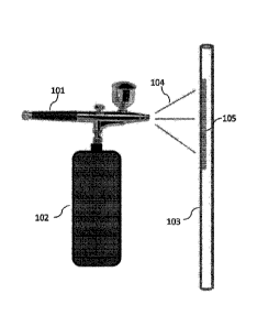
100541 FIG. IA illustrates a process for coating a polymer filament exterior
with carbon
nanotubes by spray deposition.
100551 FIG. 1B is a photograph showing the spray deposition process
illustrated in FIG. 1A.
100561 FIG. 2 is a photograph showing an alternative process for coating a
polymer filament
exterior with carbon nanotubes by dip coating.
100571 FIG. 3 is a photograph of a carbon nanotube/PLA-coated filament.
100581 FIG. 4 illustrates a process in which the coated polymer filaments
(after the spray
deposition shown in FIG. 1) are exposed to microwave heating.
100591 FIG. 5 is a photograph of polymer filaments partially coated by spray
deposition (as
shown in FIG. 1) and then exposed to microwave heating (as shown in FIG. 4).
100601 FIG. 6 illustrates polymer filaments (after the spray deposition shown
in FIG. I)
arranged in a crosshatch stack arrangement being exposed to microwaves.
100611 FIG. 7 is a photograph of a microwave-fused crosshatch stack made by
coating
polymer filaments by spray deposition (as Shown in FIG. I) and arranging and
then exposing
the crosshatch stack of coated polymer filaments to microwaves (as shown in
FiG. 6). The
magnified portion in this FIG. 7 is an optical microscope image of the
microwave-fused
crosshatch stack 701.
100621 FIG. 8 is two photographs of similarly made 3D printed objects (object
801 and
object 1102). Object 801 was made by an additive manufacturing process with
pure ABS
printer filament. Object 1102 was made by the same additive manufacturing
process with
carbon nanotube coated ABS printer filament, which was treated post-printing
with
microwave irradiation.
Date Recue/Date Received 2022-07-18
100631 FIG. 9 is a photograph of tensile dogbone samples with (902) and
without (901)
CNIs incorporated into the printing process.
100641 FIG. 10 is a photograph of compression testing samples with (1002) and
without
(1001) CNTs incorporated into the printing process. The image shows the
samples after
compression testing and the difference in compressive strength with the CNIs
and
microwave treatment applied to the sample.
100651 FIG. 11 is an SEM of a cross-sectional view of a polymer filament
coated with a
dispersion of carbon nanotubes.
100661 FIG. 12 is an SEM of the coated polymer filament of FIG. 11 (further
magnified)
showing the randomly oriented multi-wailed carbon nanotubes.
100671 FIG. 13 is an SEM of a 3D printed object (viewed from the top surface)
made by an
embodiment of the present invention (after being irradiated with microwaves).
100681 FIG. 14 is an SEM of the 3D printed object of FIG. 13 (viewed from the
top surface
and further magnified) Showing the randomly oriented multi-walled carbon
nanotubes.
100691 FIG. 15 is an SEM of a cross-section of the 3D printed object of FIG.
7.
100701 FIG. 16A is a photograph of a bundle of multi-wall carbon nanotube
coated PLA
filaments. FIG. 16B is an image from a forward-looking infrared (FLIR camera)
of the
temperature profile of the bundle of FIG. 16.A upon microwave exposure.
100711 FIG. 17 is a graph reflecting the DC conductivity (1701) and AC
conductivity (1702)
versus the multi-walled loading in PLA films.
100721 FIG. 18 is an image from a forward-looking infrared (FL1R camera) of a
PLA/multi-
walled carbon nanotube samples with a loading of 0.1 wt%.
100731 FIG. 19 is an image from a FLIR camera of a PLA/multi-walled carbon
nanotube
samples with a loading of 0.5 wt%.
11
Date Recue/Date Received 2022-07-18
100741 FIG. 20A is an image from a FLII2 camera of a PLA/multi-walled carbon
nanotube
samples with a loading of 1.0 wt%. FIG. 20B is enlarged view of the image of
FIG. 20A.
FIG. 20C is an ANSYS simulation of volume loss density (roughly proportional
to power
dissipated as heat) as a function of CNT loading of 1.0 wt% in homogeneous
polymer
nanocomposites.
100751 FIG. 21A is an image from a FUR camera of a PLA/multi-walled carbon
nanotube
samples with a loading of 2.5 wt%. FIG. 21.B is enlarged view of the image of
FIG. 21A.
FIG. 21C is an .ANSYS simulation of volume loss density as a function of CNT
loading of
2.5 wt% in homogeneous polymer nanocomposites.
100761 FIG. 22A is an image from a FL1R camera of a PLA./multi-walled carbon
nanotube
samples with a loading of 5 wt%., FIG. 228 is enlarged view of the image of
FIG. 22A.
FIG. 22C is an ANSYS simulation of volume loss density as a function of CNT
loading of 5
wt% in homogeneous polymer nanocomposites.
100771 FIG. 23A is an image from a FUR camera of a PLA/multi-walled carbon
nanotube
samples with a loading of 10 wt%. FIG. 23B is enlarged view of the image of
FIG. 23A.
FIG. 23C is an ANSYS simulation of volume loss density as a function of CNT
loading of
wt% in homogeneous polymer nanocomposites.
100781 FIG. 24 is a graph of the maximum temperature versus time of PLA/m:ulti-
walled
carbon nanotube samples (with loadings of 0.1 wt%, 0.5 wt%, I wt%, 2.5 wt%, 5
wt%, and
10 wt%).
100791 FIG. 25A is a graph of the DSC curves for neat PLA and PLA/multi-walled
carbon
nanotube (10 wt%).
100801 FIG. 25B is a graph of the DSC thermogram for neat P.LA and PLA/multi-
walled
carbon nanotube (10 wt%).
12
Date Recue/Date Received 2022-07-18
100811 FIG. 25C is a graph showing the heat capacity at constant pressure
versus
temperature for neat PLA and PLA/multi-walled carbon nanotube (10 wt%).
100821 FIG. 26 is a graph showing simulated results of the normalized
microwave absorbed
power versus the loss tangent for fixed dielectric constant of a simulated
lossy dielectric in a
rectangular waveguide with a constant dielectric constant.
100831 FIG. 27 shows the electric field magnitude in a bundle of PLA filaments
coated with
a thin conductive shell representing CNTs.
100841 FIG. 28 illustrates a schematic of peel tests for microwave enhanced
CNT/polymer
film adhesion.
100851 FIG. 29 illustrates a process of an embodiment of the present invention
wherein an
in-situ microwave applicator applies microwave energy at the point of
extrusion to control
the localized heating and welding of the polymer.
DETAILED DESCRIPTION
100861 The present invention embodies a technique for incorporating microwave
absorbing
nanomaterials (carbon nanotubes (CNTs)) onto the surface (or throughout the
volume) of 3D
printer polymer filament to increase the inter-bead bond strength following a
post microwave
irradiation treatment and/or in-situ focused microwave beam during printing.
In
embodiments of the present invention, additive manufacturing techniques, in
which
successive layers are laid down additively into the desired shape, are
utilized by 3D printers
to manufacture thermoplastic parts. These 3D printers can print intricate
product designs
much faster than regular machining techniques; however, the strength of the
final part may be
compromised when compared to parts produced through conventional machining
methods. A
treatment process of the present invention is used to address the compromise
of the strength
of the produced part as compared to parts produced through conventional
machining
13
Date Recue/Date Received 2022-07-18
methods. The treatment process is used to eradicate this weakness of 3D-
printed parts. The
treatment process includes coating the part with a carbon nanotube (CNT)-
coating and
application of microwave irradiation (often successive applications of
microwave irradiation).
The microwave irradiation can occur during the additive manufacturing process
and/or after
completion of the additive manufacturing process.
Coating Polymer Filaments
[0087] Referring to FIG. IA, FIG. IA illustrates a process for coating a
polymer filament
103 exterior with carbon nanotubes by spray deposition. In this embodiment, an
airbrush 101
that has a reservoir 102 of a carbon nanotube dispersion is used to coat the
exterior of
polymer filament 103, such as an acrylonitfile butadiene styrene (ABS)
filament. The
polymer filament 103 can be made from other polymers, such as polycarbonate
(PC),
polylactic acid (PLA), high density polyethylene (HDPE), PC/ABS, and
polyphenylsulfone
(PPSU), polyamide (nylon), high impact polystyrene (HIPS), polyetherimide
(ULTEM7m),
polyether ether ketone (PEEK), polytetrafluoroethylene (PTFE), and
combinations thereof
The carbon nanotube dispersion was made by dissolving the thermoplastic in a
suitable
solvent (acetone for ABS) at a concentration of 10 mg/ml and adding multi-
walled carbon
nanotube powder (CheapTubes.com, Brattleboro, Vermont) at a concentration of
0.5 mg/ml
followed by probe sonicating for 30 minutes. Other solvents that can be used
are, for
example, chloroform for PLA.
100881 Using the airbrush 101, a spray 104 of the carbon nanotube deposition
is applied to
polymer filament 103 to form a coating 105 upon the polymer .filament 103.
FlIG.1.13 is a
photograph showing the spray deposition process illustrated in FIG. 1A.
100891 Alternative processes to coat the exterior of polymer filament 103 with
a coating
105 include dip coating the bare filament in a bath of the CNT dispersion
(such as shown in
FIG. 2), simultaneous co-extrusion of a CNT polymer masterbatch sheath and
pure polymer
14
Date Recue/Date Received 2022-07-18
core coaxial filament, and combinations thereof. See
'U.S. Patent No. 3,458,615,
"Hydrodynamically Centering Sheath/Core Filament Spinnerette," issued July 29,
1969, to
Bragaw et al.; U.S. Patent No. 4,680,156, "Sheath Core Composite Extrusion And
A Method
Of Making It By Melt Transformation Coextrusion," issued July 14, 1987, to
Collier; and
U.S. Patent No. 5,219,508, "Method Of Manufacturing Sheath Core Fiber," issued
June 15,
1993, to Collier et al. The dip coating process shown in FIG. 2 is scalable
for creating
processing uniform filament coatings.
100901 For instance, the coating bath can be a MWCNT-OH/PLA/chloroform
dispersion. In
the case of dip coating a more viscous coating solution is used for
controlling the final
coating thickness. In one embodiment this viscosity increase is achieved by
increasing the
solids weight percent in the chloroform to 40 mg/ml of solvent. As the
filament passes
through the bath (such as shown in FIG. 2), a thin MWCNT/PLA shell is
deposited onto the
filament surface. The drying time is rapid enough such that the filament bulk
is not damaged
by the chloroform, and recovers its original mechanical properties after
vacuum drying in an
oven at 100 C for 24 hours. The filament coating can be a MWCNT/PLA composite
film
because a MWCNT-only coating would generally not be sufficiently bonded to the
surface to
survive a 3-D printing process intact.
100911 FIG. 3 is a photograph of a carbon nanotube/PLA-coated filament made
with the
dip coating process described and depicted in FIG. 2.
Carbon Nanotu.bes
100921 Types of carbon nanotubes used in the present invention include single-
wall carbon
nanotubes, multi-walled carbon nanotubes, functionalized carbon nanotubes,
etc. Other forms
of microwave absorbing nanomaterials can also be used, including carbon black,
buckyballs,
graphene, superparamagnetic or magnetic nanoparticles, metallic or
semiconducting
Date Recue/Date Received 2022-07-18
nanowires and quantum dots, and certain conductive polymers, such as
polyaniline (PAN!) or
poly3,4-ethylenedioxythiophene polystyrenesulfonate (PEDOT:PSS).
.Microwave Healing
(00931 FIG. 4 illustrates a process in which the coated polymer filaments 103
(after the spray
deposition shown in FIG. 1) are exposed to microwaves 401. Although the pure
polymer
filaments 103 are relatively insensitive to the microwaves 401, the carbon
nanotubes in the
coating 105 display an extraordinary sensitivity to microwave exposure and
these generate
localized heating. This localized heating is discussed and described, for
example, in Inn, F.,
et al., "Detection of carbon nanotubes in biological samples through microwave-
induced
heating," carbon, 2012, 50, (12), 4441-4449 and Vegesna, S., et al., "Non-
destructive
Technique for Broadband Characterization of Carbon Nanotubes at Microwave
Frequencies,"
Journal of Electromagnetic Waves and Applications, 2013, 27, (11), 1372-1381.
The
localized heating of .the microwaved carbon nanotubes causes selective fusing
at the filament-
filament interface 402, which allows for polymer diffusion and formation of a
continuous
polymer structure that is markedly different than the native, as-printed, 3D
structure. The
polymer filaments 103 are able to fuse at the filament-filament interface 402
once adjacent
polymer filaments 103 wet at the filament-filament interface 402 and the
polymer chains are
able to inter-diffuse across the interface. For example, polymer filaments 103
can wet at the
filament-filament interface 402 by melting or, for polymers that do not melt
(such as
amorphous polymers), they can flow as non-Newtonian fluids when the polymer
filament 103
is raised to a temperature significantly above its glass transition
temperature.
100941 The microwaves can be applied during or after the 3D printing process.
In some
embodiments, the microwaves 401 are applied during post-fabrication of the
object once the
additive manufacture process is complete. In other embodiments, the microwaves
are applied
as the successive layers are being laid down (i.e., an "in-situ" process).
Such an in-situ
16
Date Recue/Date Received 2022-07-18
process can be employed by a focused microwave beam to heat the filament-
filament
interface during the printing process itself, which integrates the microwave
exposure system
into the 3D printer hardware (with appropriate electromagnetic shielding).
"Welding" these
filament-filament interfaces during manufacture strengthens the structure. An
additional
benefit is that this process enables certain shapes previously unattainable by
conventional
extrusion deposition processes to be manufactured. For instance, an extrusion
deposition
process typically cannot produce overhanging structures or large gaps, since
they would be
unsupported during the build. Although large unsupported bridging has been
demonstrated
*(http://www.thingiverse.comith ing:12925, http://youtu.beLboliFFcLh_Q
and
http://youtu.be/wK2APNwEoSk)*, printing additional layers over the bridge
generally results
in sagging due to the latent heat of the subsequent polymer bead and the added
weight. By
increasing the strength of the welds during the 3D printing process with the
invention
described herein, such bridge-like structures may be obtained with better
dimensional
tolerances. This is important for complex parts, where significant amounts of
break-away or
dissolvable support material are typically utilized.
Polymer Filament Bundle
100951 FIG. 5 is a photograph of a polymer filament bundle 501 of polymer
filaments 103
partially coated (with coating 105) by spray deposition (as shown in FIG. 1)
and then
exposed to microwave heating (as shown in FIG. 4). The polymer filaments 103
were made
of ABS and were exposed with microwaves 401 (at around 2.45 GHz for around 20
seconds
in a conventional microwave oven) to form a fused structure with minimal air
gaps between
the filaments (in the coated section of the polymer filaments 103). In
contrast, the uncoated
portion of the polymer filaments 103 (i.e., the microwave transparent .ABS
filament portions)
were unaffected by the microwave treatment process 401 and did not fuse
together.
17
Date Recue/Date Received 2022-07-18
Crosshatch Stack
100961 FIG. 6 illustrates polymer filaments 103 (after the spray deposition
shown in FIG. 1
to form coating 105 on the exterior) arranged in a crosshatch stack
arrangement being
exposed to microwaves 401. FIG. 7 is a photograph of a microwave-fused
crosshatch stack
701 made by coating polymer filaments by spray deposition (as shown in FIG. 1)
and
arranging and then exposing the crosshatch stack of coated polymer filaments
to microwaves
(as shown in FIG. 6). Magnified portion 702 is an optical microscope image of
the
microwave-fused crosshatch stack 701. The polymer filaments 103 were ABS. The
crosshatch stack of coated polymer filaments 103 were exposed with microwaves
401 (at
around 2.45 GHz for around 20 seconds in a conventional microwave oven) to
form a fused
structure with minimal air gaps between the filaments. This filament fusion
that occurs
during the microwave exposure eliminates voids and improves load transfer.
100971 Variables in this process include irradiation time, power, frequency,
thickness of the
CNT polymer sheath, CNT weight or volume fraction in the coating, and the
coating process
itself. In some embodiments, the irradiation time is between about I second
and about 5
minutes, the irradiation power is between about 1 W and about 1 kW, and the
CNT polymer
sheath thickness is between about 100 nm and about 0.5 mm. Frequency of the
microwaves
can be controlled by the type of microwave source utilized.
Printed Object
100981 FIG. 8 is two photographs of similarly made 3D printed objects (object
801 and
object 802). Object 801 was made by an additive manufacturing process with
pure ABS
printer filament. Object 802 was made by the same additive manufacturing
process with
carbon nanotube coated ABS printer filament, which was treated post-printing
with
microwave irradiation.
18
Date Recue/Date Received 2022-07-18
100991 With regard to object 802, the carbon nanotube dispersion was sprayed
onto the pure
ABS printer filament using an airbrush and then exposing the carbon nanotube
coated printed
part to microwaves at around 2.45 GHz for around 15 seconds in a conventional
microwave
oven. As with the other objects formed using embodiments of the present
invention, this
process formed a fused structure (object 1102) with minimal air gaps between
the filaments.
1001001 FIGS. 9-10 are photographs of other 3D printed objects made
from coated
filaments. Objects 901 and 1001 are 3D printed objects made with only pure
uncoated PLA
printer filament. These were printed using an UP! Mini 3D Desktop Printer.
Object 902
and 1002 are these 3D printed objects with the CNT coating applied and after
exposure to
microwaves.
Morphology
1001011 FIG. 11 is an SEM of a cross-sectional view of a polymer
filament 1101.
coated with a dispersion of carbon .nanotubes. The polymer filament 1101 is
pure ABS. The
coated polymer filament has not been irradiated with microwaves. The carbon
nanotube
coating 1102 (the coaxial CNT Sheet) has a thickness 1103 of around 15 1.tm.
FIG. 12 is an
SEM. of coated polymer filament 1101 (further magnified) showing the randomly
oriented
multi-walled carbon nanotubes 1201 in carbon nanotube coating 1102.
1001021 FIG. 13 is an SEM of a 3D printed object (viewed from the top
surface) made
by an embodiment of the present invention (after being irradiated with
microwaves). FIG. 13
shows the interface 1302 between two extruded polymer beads 1301. FIG. 14 is
an SEM of
the 3D printed object of FIG. 13 (viewed from the top surface and further
magnified)
showing the randomly oriented multi-walled carbon nanotubes 1401 in the carbon
nanotube
coating. The multi-walled carbon nanotubes have diameters between around 50 nm
and
around 80 nm. FIG. 15 is an SEM of a cross-section of the 3D printed object of
FIG. 7.
19
Date Recue/Date Received 2022-07-18
This cross-section shows the polymer filament 1501 (pure ABS), carbon nanotube
coating
1502, and interface 1503 between the extruded polymer beads.
1001031 A comparison between the multi-walled carbon nanotubes 1201
(before
irradiation with microwaves) in FIG. 12 and the multi-walled carbon nanotubes
1401 (after
irradiation with microwaves) in FIG. 14 shows that the microwave irradiation
process does
not significantly damage or destroy the multi-walled carbon nanotubes.
1001041 Additionally, the post treatment images of FIGS. 13-15 shows
the carbon
nanotubes and polymer are in good contact and there is no visible bubbling or
damage (i.e.
burning) of the polymer. This revealed that the carbon nanotubes likely
transferred (via
conduction) their intense heat profile to the polymer and dissipated this heat
to fuse the
polymer interface without causing significant degradation.
Heat Response To Microwave Radiation
1001051 Microwave-induced CNT heating opcnN up tlic possibility of
tunable polymer
mobility and adhesion in polymer nanocomposite interfaces. This phenomenon
could also be
used to improve these polymer welds in 3-D printed parts. By connecting
dielectric properties
with in situ microwave thermometry, the present invention can control how the
microwave
response affects polymer film and filament adhesion in an additive
manufacturing context.
1001061 It has been discovered that there is a non-linear, non-
monotonic microwave
absorbance response in the filaments as a function of carbon nanotube loading.
Above a
threshold carbon nanotube loading, the heating response increased sharply,
indicating that the
carbon nanotubes' microwave response is affected by carbon nanotube network
connectivity
(percolation). This was unexpected and not previously reported.
1001071 It is believed that the heating response of CNT-loaded polymer
nanocomposites is non-linear and non-monotonic because of the dielectric
properties of
Date Recue/Date Received 2022-07-18
electrically percolating CNT networks (i.e., due to a connection between
microwave heating
adsorption and the dielectric properties of the CNT/polymer nanocomposites).
1001081 Polyactic acid (PLA), which is commonly utilized in additive
manufacturing,
was mixed with commercially available multi-walled carbon nanotubes at various
weight
percentages. For example, -OH functionalized multi-walled carbon nanotubes
were dispersed
in a VLA/chloroform solution and these dispersions were used to solution cast
and hot press
MWCNT/PLA films at varying levels of MWCNT loading between 0.00 and 10.0
weight
percent. After casting these films, characterization of these included DC and
AC electrical
property testing, infrared thermometry (effectively using imaging to carry out
in situ
microwave calorimetry), and Differential Scanning Calorimetry (DSC).
1001091 These measurements indicated a dramatic increase in microwave
absorbance
at MWCNT loadings above the electrical percolation threshold. It is believe
that this increase
in heating response is caused by a transition from a disconnected network of
the conducting
carbon nanotubes to a connected network. The induced electric current
magnitudes on the
carbon nanotubes due to microwave radiation are significantly increased above
this threshold,
resulting in high power dissipation through heating. It is further believed
that below this
threshold, the gaps between the carbon nanotubes in the disconnected network
inhibit current
flow due to the high impedances in the matrix.
1001101 FIG. 16A is a photograph of a bundle of multi-wall carbon
nanotube coated
PLA filaments. FIG. 168 the .FLIR for microwave exposure of a bundle of the
MWCNT-
coated PLA filaments (198 W, 20 seconds of exposure), the selected video frame
shows the
heating profile after 0.1 seconds of exposure and the depicted I 7 C rise in
temperature (from
18 C to 35 C) illustrates the rapidness of the heating process. The data show
localized
heating effects, confirming that the heating is restricted to the MWCNT-
enriched regions,
promoting inter-filament welds, similar to simulation results in FIG. 27
(discussed below).
21
Date Recue/Date Received 2022-07-18
Over the course of the analysis, the spatially averaged sample temperature
rose by 58.5 C.
This data in FIG. 16B indicate that the prospect of coating the filament with
microwave-
responsive CNTs is effective.
Electrical Properties
100111.1 The
heating can be tailored based upon the electrical properties of the resulting
film. Such electrical properties include conductivity, loss tangent, and
dielectric properties.
1001121 The DC
and AC conductivities of the PLA films loaded with various multi-
walled carbon nanotube loadings were measured. DC measurements were conducted
using a
four-point-probe. These AC measurements were performed with a low-power
microwave
network analyzer using coaxial lines and rectangular waveguides on the
PLA/multi-walled
carbon nanotube samples (rectangular PLA/multi-walled carbon nanotube samples,
0.5 mm
thick, inserted in a
rectangular waveguide). The scattering parameters (transmission and
reflection coefficients) were measured using an Agilent microwave network
analyzer and
were used to extract the dielectric properties of the samples after proper
calibration. Since a
waveguide was used for the measurements, a thru-reflect-line CTRL calibration)
was
performed to correct for the coax to waveguide adapters and input and output
waveguide
sections.
1001131 FIG.
17 is a graph reflecting the DC conductivity (1701) and AC conductivity
(1702) versus the multi-walled nanotube weight percent loading in PLA films,
As shown in
FIG. 17, the AC (at .2.45 GHz) and DC conductivity values are the same for
percolated,
resistive carbon nanotube networks at high carbon nanotube loading (greater
than 5 wt%), but
AC conductivity is higher at low carbon nanotubc loading (less than 3 wt%).
1001141 Other
microwave material characterization methods (such as using coaxial
lines that operate over a very broad frequency range - from DC to microwaves)
can be used
to yield dielectric constant and conductivity data. Such data can be used to
determine optimal
22
Date Recue/Date Received 2022-07-18
carbon nanotube concentrations needed, and may reveal frequency dependent
features
(resonances) Which can be exploited for tailoring the heating response.
Ternnerature Profile
1001151 Temperature profiles of the PLA/multi-walled carbon nanotube
samples set
forth above were also examined to show their thermal response to high power
(10-100 W)
microwave radiation at 2.45 GHz in a controlled environment. The in-situ
microwave
calorimetry setup used a forward-looking infrared (FUR) camera to image the
temperature
increase at the center of the homogeneous films placed inside a rectangular
waveguide, which
in turn was connected to a microwave generator. (FLIRit Systems, Inc.). The
FLIR looks at
the sample through a metal mesh window covering the open end of the waveguide.
An
electromagnetic RF meter is used to ensure safety during microwave radiation.
1001161 PLA/multi-walled carbon nanotube samples (with loadings of 0.1
wt%, 0.5
wt%, 1 wt%, 2.5 wt%, 5 wt%, and 10 wt% were tested. The FLIR camera showed
thermal
images of PLA films (inside the waveguide) at varying MWCNT loadings after 30
seconds of
20 W microwave exposure at 2.45 GHz in a custom waveguide. FIGS. 18, 19, 20A,
21A,
22A, and 23A. As shown in these Figures, the heating response dramatically
increases as the
loading is increased to 2.5 wt% carbon nanotubes. It is believed that this was
related to the
onset of a resistive (rather than capacitive) percolating network.
1001171 FIGS. 22A and 23A also show that the heating responses
decreases (and
changed in spatial distribution) as the loading changes from 5 wt% to 10 wt%.
It is further
believed that this is related to the transition from power absorbance to
microwave power
reflectance associated with high conductivity networks. The unusual, non-
monotonic heating
progression indicates an overall picture of microwave power transmission (in
sub-percolation
samples), microwave power absorbance (samples with nanofiller loadings just
above
23
Date Recue/Date Received 2022-07-18
percolation), and microwave power reflectance in highly conductive samples.
This further
indicates a beneficial range of CNT content for microwave heating.
100118j .FIG. 24 shows the maximum temperature versus time of the
PLA/multi-
walled carbon nanotube samples (with loadings of 0.1 wt%, 0.5 wt%, 1 wt%, 2.5
wt%, 5
wt%, and 10 wt%) (2401-2406, respectively).
Differential Scanning Calorimetry
1001191 Differential Scanning Calorimetry (DSC) was used to measure
the melting
point, crystallization temperature and glass transition temperatures of the
neat PLA and
PLA/multi-walled carbon nanotube samples set forth above. FIG. 25A shows the
DSC
curves for neat PLA (2501) and .PLA/multi-walled carbon nanotube (10 wt%)
(2502). FIG.
25A shows the DSC thermogram for neat PLA (2503) and PLA/multi-walled carbon
nanotube (10 wt%) (2504). These measurements indicate the precise temperatures
at which
the polymer is likely to form strong welded interfaces. Most thermoplastic
polymers must be
heated beyond their glass transition temperature in order to form a bond or
weld. The 'DSC
also yielded estimates of the differentiable heat capacity as a function of
temperature that
correlated with the results of the temperature profiles obtained through FUR
imaging. FIG.
25C shows the heat capacity at constant pressure versus temperature for neat
PLA (2505) and
PLA/multi-walled carbon nanotube (10 wt%) (2506). The .DSC measurements
indicated that
the Tg of the .PLA is correlated with a plateau in the dynamic temperature
versus time
response in the FLIR-imaged samples (-60 C).
Microwave interaction With Carbon Nanotube-Loaded Polymers
1001201 The heating behavior of the microwaves is based on the sample
geometry, the
applied electromagnetic field and the materials' dielectric properties.
Simulation and
modeling was utilized to investigate the underlying science of microwave
response of CNT-
24
Date Recue/Date Received 2022-07-18
loaded polymers. Simulation and modeling aids in the investigation of the
effect of various
parameters (CNT loading, microwave power, sample thickness) on the heating
response.
1001211 Modeling microwave heating involves electromagnetic modeling
as well as
thermal/heat transfer modeling. Commercial software from ANSYS (High Frequency
Structure Simulator, HFSS) for the electromagnetic simulation coupled with
ANSYS
Mechanical for the thermal simulation is utilized. COMSOL Multiphysics is also
utilized for
comparison with ANSYS results. Modeling CNT-loaded polymers exposed to
microwaves is
a challenging problem due to the drastic difference between the dimensions of
CNTs
(nanometers) and the bulk sample (centimeters). Direct simulation is not
possible due to the
vast computational resources needed.
1001221 Simulation results using ANSYS HFSS are shown in FIGS. 20C,
21C, 22C,
and 23C (alongside experimental data for comparison in FIGS. 20B, 218, 22B,
and 23B,
respectively) for simulations of slabs of a Iossy dielectric in a rectangular
waveguide. The
loadings of the samples in the simulations of FIGS. 20C, 21C, 22C, and 23C
(and
experiments of FIGS. 20B, 21B, 228, and 23B) were 1 wt%, 2.5 wt%, 5 wt%, and
10 wt%,
respectively. The simulations required an input value of loss tangent, which
was
experimentally measured for samples of varying CNT loading. The loss tangent
and dielectric
constant for these samples were taken from waveguide measurements on the
nanocomposite
films with varying CNT loading. These measured loss tangent and dielectric
constant values
were used for the simulations, and the resulting spatial distributions again
show the
microwave transmission, absorbance, and reflectance.
1001231 The similarity between the two datasets (of (a) FIGS. 20C,
21C, 22C, and
23C and (b) FIGS. 20B, 21B, 228, and 23B) was remarkable. As CNT loading
increased,
the samples' microwave response underwent two transitions: from power
transmission to
Date Recue/Date Received 2022-07-18
absorbance to reflectance. This remarkable agreement between simulation and
experiment
for CNT/microwave interactions is completely new and not previously reported.
1001241 The relationship between carbon nanotube concentration and
total absorbed
power was computed for tuning the microwave absorption in the carbon nanotube
layer.
ANSYS HFSS was used to simulate a slab of a lossy dielectric placed in a
rectangular
waveguide with a constant dielectric constant. FIG. 26 shows the total
normalized
microwave power absorbed by the slab versus the material's loss tangent tan5
(the loss
tangent is related the material's electrical conductivity tan6 =a1(27rfc),
where a is the
conductivity, 6 is the dielectric constant, and .fis the frequency). As shown
in FIG. 24, there
is an optimum value for the loss tangent (controlled by the CNT concentration
amount) that
maximizes the power dissipated in the material (converted to heat). This can
be used to
identify the parameters for achieving the desired bonding strength in the
manufactured
components using the CNT/PLA substrates after microwave exposure. Such
parameters
include CNT concentration, microwave power, frequency, and exposure time.
1001251 This modeling and simulation also indicated the inhomogeneous
heating
effects in the nanocomposites. FIG. 27 shows the electric field magnitude in a
bundle of
PLA filaments coated with a thin conductive shell representing CNTs (shown in
:FIGS. 1.6A-
I6B). The bundle was placed in a rectangular waveguide operating in TElo mode
which has a
vertically polarized electric field. The amount of heating corresponded to the
electric field
magnitude. The electric field was stronger in the thin CNT shell region than
in the FLA core,
resulting in stronger heating of the shell. This indicates that the heating
was confined to the
shell, allowing for heating and diffusion at the interface rather than the
bulk.
Nilo-cm aye-Induced Polymer Adhesion
1001261 The mechanical effects of microwave heating on welds in
CNT/polymer
nanocomposites were also examined. The CNT-rich polymer coatings enhance
polymer
26
Date Recue/Date Received 2022-07-18
substrate adhesion upon exposure to microwave irradiation. In addition to
polymer interface
mechanics, such phenomena open up new avenues in additive manufacturing by
allowing
site-specific heating/bonding at the nanoscale.
1001271 To examine this, MWCNT/PLA films were applied on two PLA
substrates,
the two substrates were then adhered, and then exposed the sample to a
microwave field. A
commercial 1250 W microwave oven for microwave exposure was utilized. Since
microwave
ovens do not have a uniform electromagnetic field distribution, the sample
experienced
inhomogeneous heating. However, a microwave exposure chamber can be utilized
that
provides uniform electromagnetic field distribution to better ensure that the
parts of the
sample are uniformly heated.
1001281 As the multi-walled carbon nanotubes act as local heat sources
when exposed
to microwaves, polymer diffusion and increased mobility at the interface will
allow for
seamless weld, forming rapidly without warping the bulk structure. ASTM peel
tests
(conducted using a conventional tensile tester) as illustrated in FIG. 28 can
provide a
macroscale indication of the effect of microwave irradiation on the enhanced
adhesive
strength in the MWCNT/polymer layer. The coating thickness and CNT content can
be varied
(as well as the microwave exposure) to control the effects of the coating on
polymer
diffusion. In addition to the non-monotonic microwave response of the CNT
film, it is
believed that extremely high CNT loadings will inhibit polymer diffusion from
the two bulk
phases on either side of the interface. Accordingly, the coating thickness and
CNT content
can be controlled for better polymer diffusion. Hence the degree of chain
inter-diffusion and
effectiveness of the welding process is tunable and controllable.
Manufacturing Process
1001291 The process of coating normal PLA filaments with carbon
nanotubes allows
that these PLA filaments can be used in existing 3-D printers. The concept of
coating
27
Date Recue/Date Received 2022-07-18
filaments with carbon nanotubes for microwave-induced welding is entirely new.
The data
indicate such coated filaments can be used as a feedstock for 3-D printing a
variety of
structures. For instance, these CNT-loaded 3-D structures can be formed and
then be
exposed to microwave irradiation (in the range of 1W to 11W) for a period of
time (in the
range of I second to 5 minutes) such that the CNT-rich polymer coatings will
be heated and
induce localized melting, interfacial diffusion, and increased adhesive
strength. These can be
controlled for advanced properties, including those reflected above. The
resulting objects can
have (by design) enhanced compressive and tensile strength (such as can be
measured on an
histron mechanical tester).
1001301 The data (reflected above) show that the CNT coating is
maintained
throughout the extrusion process that occurs during 3-D printing. These
structures have
similar surface conductivity and microwave responsiveness before and after
printing if both
CNT and PLA are present in the coating.
1001311 FIG. 29 illustrates an in-situ microwave magnetron-waveguide-
coaxial
applicator system 2901 to heat the filament-filament interface at the newly
printed location
during the printing process itself that can be utilized in an embodiment of
the present
invention. In system 2901, the printing 'filament 2902 (such as carbon
nanotube coated FLA)
is extruded through the extruder nozzle 2903 of the additive manufacturing
device (such as a
3D printer, i.e., like the 3D printer produced by Helix). an FIG. 29 only the
extruder nozzle
2903 and the printing filament 2902 of the additive manufacturing device is
shown in detail.
The remainder of the standard additive manufacturing device, such as the
standard parts of a
3D printer are represented by block 2904).
1001321 System 2901 also has a microwave source 2904 (such as a
rectangular
waveguidc that has a 2.45 GHz microwave input (controllable with a frequency
tuning
plunger). The microwave source can be focused upon the newly printed location
using a
28
Date Recue/Date Received 2022-07-18
coaxial applicator tip 2905 located at that location. The application of
microwaves at the
coaxial locator tip provides localized heating (AT) 2906.
1001331 Electromagnetic shielding (not shown) can also be incorporated
into the
system for various reasons, including safety and integrity concerns.). This
allows the
microwave exposure system to be integrated into the 3-D printer hardware with
appropriate
electromagnetic shielding measures.
1001341 The coaxial applicator tip 2905 can be attached to the printer
head directly
(which is where the extruder nozzle 2903 is located) in order to move with the
printer head.
This localized microwave heating allows for the microwave power to be applied
during
printing, with only the immediately-printed area being exposed rather than the
entire sample.
1001351 This will allow for direct modifications to the printer
architecture to allow for
microwave exposure immediately after filament deposition.
1001361 Such a system will yield (a) a novel system and process that
utilizes
microwave radiation response of CNTs and CNT/polymer nanocomposites; (b)
efficient
modeling techniques suitable for materials with CNT dispersions; (c)
processing-structure-
property relations for CNT/polymer nanocomposite welds after microwave
exposure; (d)
development of a 3D printing apparatus incorporating optimized CNT loading and
a
microwave exposure process.
Manufacturin Tech o lo tn.
1001371 Embodiments of the present invention overcome the current disparity
between (1)
traditionally manufactured polymer parts utilizing injection molding,
extrusion molding,
machining and (2) parts printed with additive manufacturing techniques such as
Fused
Deposition Modeling (FDMTm, Stratasys, inc.) and Fused Filament Fabrication
(FFF). Such
processes (a) increase the overall strength of 3D printed thermoplastic parts,
(b) allow for the
rapid diffusive bonding of polymer chains between beads (thus increasing
strength), without
29
Date Recue/Date Received 2022-07-18
distorting or heating the bulk part, and (c) improve the isotropic mechanical
properties of 3D
printed thermoplastic parts so that they can rival (Cr even exceed) their
manufactured
counterparts.
100011 Embodiments of the present invention can be used and incorporated into
industrial
and consumer 3D printing processes. Embodiments of the present invention can
enhance the
manufacturing of parts, such as parts pertaining to the aerospace, automotive,
defense, and
space industries.
1001381 The system and processes of the present invention and the resulting
materials
produced are important for a range of engineering fields, both fundamental
(such as polymer
dynamics, microwave physics) and applied (nanocomposite processing). These
outcomes
dovetail with national manufacturing priority areas including additive
manufacturing, vehicle
and antenna design, radar-absorbing coatings, and electromagnetic shielding.
Defense and
aerospace needs in particular have substantial needs that can be met by
additive
manufacturing if the difficulties with weld mechanical properties are also
addressed.
1001391 The present invention also has significant impact on other industrial
and scientific
applications that utilize nanoparticies for electrical property modification.
Accurate and
efficient nanoparticle dispersions in a host medium to controllably utilize
their electrical
properties is a challenging problem and is very much needed in multitude of
applications.
1001401 The examples provided herein are to more fully illustrate some of the
embodiments
of the present invention. It should be appreciated by those of skill in the
art that the
techniques disclosed in the examples which follow represent techniques
discovered by the
Applicant to function well in the practice of the invention, and thus can be
considered to
constitute exemplary modes for its practice. However, those of skill in the an
should, in light
of the present disclosure, appreciate that many changes can be made in the
specific
Date Recue/Date Received 2022-07-18
embodiments that are disclosed and still obtain a like or similar result
without departing from
the spirit and scope of the invention.
1001411 While embodiments of the invention have been shown and described,
modifications
thereof can be made by one skilled in the art without departing from the
spirit and teachings
of the invention. The embodiments described and the examples provided herein
are
exemplary only, and are not intended to be limiting. Many variations and
modifications of the
invention disclosed herein are possible and are within the scope of the
invention.
Accordingly, other embodiments are within the scope of the following claims.
The scope of
protection is not limited by the description set out above.
RELATED PATENTS AND PUBLICATIONS
1001421 The following patents and publications relate to the present
invention:
1001431 U.S. Patent No. 7,754,054, "Microwave Induced Functionalization Of
Single Wall
Carbon Nanotubes And Composites Prepared Therefrom," issued July 13, 2010, to
Mittra et
1001441 'U.S. Patent No. 8,080,199, "Interaction Of Microwaves With Carbon
.Nanotubes To
Facilitate Modification," issued December 20, 2011, to Tour et al.
1001451 .U.S. Patent Publication No. 2011/0223343, "Novel Nanocomposite For
Sustainability of Infrastructure," published September 15, 2011, to Wang et.
al.
1001461 Chowdhury, S. R., et al., "Microwave-induced Rapid Nanocomposite
Synthesis
Using Dispersed Single-Wall Carbon Nanotubes as the Nuclei," Journal of
Materials
Science, 2009,44, (5), 1245-1250, doi:10.1007/s10853-009-3259-4.
1001471 Higginbotham, A. L., et al., "Carbon .Nanotube Composite Curing
through
Absorption of Microwave Radiation," composites Science and Technology, 2008,
68, (15-
16), 3087-3092, doi:10.1016/j.compscitech.2008.07.004.
31
Date Recue/Date Received 2022-07-18
1001481 inn, F., et al., "Detection of carbon nanotubes in biological samples
through
microwave-induced heating," Carbon, 2012, 50, (12), 4441-4449.
1001491 Nikzad, M, et al., "Thermo-Mechanical Properties of a Highly Filled
Polymeric
Composites for Fused Deposition Modeling," Materials Design, 2011, 32, (6),
3448-3456,
doi:10.1016/j. matdes.2011.01.056.
1001501 Partain, S.C., "Fused Deposition Modeling with Localized Pre-
Deposition Heating
Using Forced Air," Vasa, 2007,
http://medcontent.metapress.com/index/A65RMO3P4874243N.pdf;
Montana .. State
University, 2007, http://scholarworks.montana.cdu/xmlui/handle/1/2016.
1001511 Paton, Keith R., et al., "Efficient Microwave Energy Absorption by
Carbon
Nanotubes," Carbon, 2008, 46, (14), 1935-1941,
doi:10.1016/j.carbon.2008.08.001.
1001521 Shim, Hyung Chcoul, et al., "Enhancement of Adhesion Between Carbon
Nanotubes and Polymer Substrates Using Microwave Irradiation," Scripta
Materialia, 2009,
61, (1), 32-35, doi:10.1016/j.scriptamat.2009.02.060.
1001531 Shofner, M.L., "Nanofiber-reinforced Polymers Prepared by Fused
Deposition
Modeling, Journal of Applied Polymer Science, 2003, 89, (11), 3081-3090
http://online1ibrary.wiley.comidoi/10.11002/app.12496/full.
1001541 Vcgesna, S., et rd., "Non-destructive Technique for Broadband
Characterization of
Carbon Nanotubes at Microwave Frequencies," Journal of Electromagnetic Waves
and
Applications, 2013,27, (11), 1372-1381.
1001551 Wang, C.Y., et al., "Strong Carbon-Nanotube¨Polymer Bonding by
Microwave
Irradiation," Advanced Functional it laterials, 2007, 17,
(12), 1979-1983,
doi: 1 0.1002/adfm.200601011.
32
Date Recue/Date Received 2022-07-18
100156j Wang, C. Y., etal., "Flexible Field Emitter Made of Carbon Nanotubes
Microwave
Welded onto Polymer Substrates," Applied Physics Letters, 2007, 90, (10),
103111,
doi:10.1063/1.2711771.
1001571 Wohlers Associates, "Wohlers Report 2012: Additive Manufacturing and
3d
Printing, State of the Industry." 2012, 1-271 (Ft. Collins, Co.)
lutp://wohlersassociates.com/state-of-the-industry-reports.html.
100158] Ziemian, C., et ai., "Anisotropic Mechanical Properties of ABS Parts
Fabricated by
Fused Deposition Modelling" Mechanical Engineering, 2012, Chapter 7, 159-181
(edited by
Gokcek, Murat), doi: 10.5772/34233.
33
Date Recue/Date Received 2022-07-18