Note: Descriptions are shown in the official language in which they were submitted.
CA 03169081 2022-08-12
1
Flat Security Element With Optical Security Features
FIELD OF THE INVENTION
The invention relates to a flat security element with optical security
features, comprising at least
one first surface region with a first sub-wavelength structure, wherein the
structure elements that
define the first sub-wavelength structures periodically repeat in the plane of
the security element.
The periodic repeating can occur in one direction, that is, in one dimension,
for example if a
structure element comprises a straight wall and multiple walls of this type
are periodically
arranged next to one another. The periodic repeating can occur in two
directions, that is, in two
dimensions, for example if a structure element comprises a column and multiple
columns are
arranged in a grid pattern, or if one structure element comprises a depression
and multiple
recesses are arranged in a grid pattern.
PRIOR ART
Relevant security elements which comprise sub-wavelength structures are known
from DE 10
2012 015 900 Al. Namely, the flat security element comprises in a first
surface region what is
referred to as a ground element structure, which due to the sub-wavelength
structure conveys
different color impressions from the front and back sides in a plan view, and
also comprises the
ground element structure in a second surface region, but in a form mirrored
from the first surface
region, whereby the first and second region show a motif from both sides in a
plan view, but the
motif is not recognizable in a transmission view. To realize the ground
element structure, a
grating ground structure in the first surface region and an inverted grating
ground structure in the
second surface region are then disclosed in a first variant. As a second
variant, a substrate with
interference coatings inverted from one another is shown in the first and in
the second surface
region.
DE 10 2012 015 900 Al thus makes it possible to convey a motif in a plan view,
that is, when
there is reflection on a surface of the security element, using two different
color impressions as a
CA 03169081 2022-08-12
2
result of the two different surface regions with a ground element structure
inverted from one
another.
SUMMARY OF THE INVENTION
It is an object of the invention to provide an alternative security element
with optical security
features, which element exhibits an increased forgery protection, is easy to
produce, and can also
convey a motif using at least two different color impressions.
The starting point of the invention is a flat security element with optical
security features,
comprising at least one first surface region with a first sub-wavelength
structure, wherein the
structure elements that define the first sub-wavelength structure periodically
repeat in the plane
of the security element. In order to alter the color effect that is produced
by a sub-wavelength
structure, it is envisaged that the first sub-wavelength structure of at least
one partial region of
the first surface region is additionally provided with an interference coating
for producing a
color-shifting effect.
In the color-shifting effect, the color impression changes with the viewing
angle; that is, the
interference coating changes the color depending on the viewing angle.
This additional interference coating causes a further change in the color
effect that results from
the sub-wavelength structure. Because the effects overlap due to the sub-
wavelength structure
and the interference coating, this cumulative effect is difficult to produce
using other methods,
which increases the forgery protection of the security element according to
the invention.
In this case, a thin-layer arrangement which causes a color-shifting effect by
means of thin-layer
interference is to be understood as an interference coating for producing a
color-shifting effect.
Security elements which are based on thin-layer interference are known from EP
1 558 449 A,
for example. An interference coating for producing a color-shifting effect,
hereinafter referred to
in short as interference coating, is normally composed of at least two partial
layers: one dielectric
CA 03169081 2022-08-12
1
3
layer and one absorber layer. An additional reflective layer on the other side
of the dielectric
layer, that is, opposite from the absorber layer relative to the dielectric
layer, reflects
electromagnetic waves, light in the visible range in this case, and thereby
intensifies the
interference effect. The dielectric layer serves as a spacer layer, if need be
between the reflective
layer and absorber layer. The color-shifting effect emerges when the
interference coating is
viewed from the absorber layer side, that is, when light falls onto the
dielectric layer through the
absorber layer.
For the dielectric layer of the interference coating, dielectric materials
with a refractive index
less than or equal to 1.65 are possible, for example aluminum oxide (A1203),
metal fluorides, for
example magnesium fluoride (MgF2), aluminum fluoride (A1F3), silicon oxide
(Si0), silicon
dioxide (SiO2), cerium fluoride (CeF3), sodium aluminum fluoride (for example,
Na3A1F6 or
Na5A13F14), neodymium fluoride (NdF3), lanthanum fluoride (LaF3), samarium
fluoride (SmF3),
barium fluoride (BaF2), calcium fluoride (CaF2), lithium fluoride (LiF), low-
refractive organic
monomers, and/or low-refractive organic polymers.
However, for the dielectric layer of the interference coating, dielectric
materials with a refractive
index greater than 1.65 are also possible, for example zinc sulfide (ZnS),
zinc oxide (Zn0),
titanium dioxide (TiO2), carbon (C), indium oxide (In203), indium tin oxide
(ITO), tantalum
pentoxide (Ta205), cerium oxide (Ce02), yttrium oxide (Y203), europium oxide
(Eu203), iron
oxides such as iron(II,III) oxide (Fe304) and iron(III) oxide (Fe2O3) for
example, hafnium nitride
(HfN), hafnium carbide (HfC), hafnium oxide (Hf02), lanthanum oxide (La203),
magnesium
oxide (MgO), neodymium oxide (Nd203), praseodymium oxide (Pr6O1I), samarium
oxide
(Sm203), antimony trioxide (Sb203), silicon carbide (SiC), silicon nitride
(Si3N4), silicon
monoxide (Si0), selenium trioxide (Se203), tin oxide (Sn02), tungsten trioxide
(W03), high-
refractive organic monomers, and/or high-refractive organic polymers.
A metallic layer can be used as an absorber layer of the interference coating,
with this being a
pure metal layer or a layer containing metallic clusters, for example.
Preferably, the absorber
layer comprises at least one metal of the group composed of aluminum, gold,
titanium,
CA 03169081 2022-08-12
3
layer and one absorber layer. An additional reflective layer on the other side
of the dielectric
layer, that is, opposite from the absorber layer relative to the dielectric
layer, reflects
electromagnetic waves, light in the visible range in this case, and thereby
intensifies the
interference effect. The dielectric layer serves as a spacer layer, if need be
between the reflective
layer and absorber layer. The color-shifting effect emerges when the
interference coating is
viewed from the absorber layer side, that is, when light falls onto the
dielectric layer through the
absorber layer.
For the dielectric layer of the interference coating, dielectric materials
with a refractive index
less than or equal to 1.65 are possible, for example aluminum oxide (Al2O3),
metal fluorides, for
example magnesium fluoride (MgF2), aluminum fluoride (A1F3), silicon oxide
(Si0), silicon
dioxide (SiO2), cerium fluoride (CeF3), sodium aluminum fluoride (for example,
Na3A1F6 or
NasAl3F14), neodymium fluoride (NdF3), lanthanum fluoride (LaF3), samarium
fluoride (SmF3),
barium fluoride (BaF2), calcium fluoride (CaF2), lithium fluoride (LiF), low-
refractive organic
monomers, and/or low-refractive organic polymers.
However, for the dielectric layer of the interference coating, dielectric
materials with a refractive
index greater than 1.65 are also possible, for example zinc sulfide (ZnS),
zinc oxide (Zn0),
titanium dioxide (TiO2), carbon (C), indium oxide (In203), indium tin oxide
(ITO), tantalum
pentoxide (Ta205), cerium oxide (Ce02), yttrium oxide (Y203), europium oxide
(Eu203), iron
oxides such as iron(II,III) oxide (Fe304) and iron(III) oxide (Fe2O3) for
example, hafnium nitride
(HfN), hafnium carbide (HfC), hafnium oxide (Hf02), lanthanum oxide (La203),
magnesium
oxide (MgO), neodymium oxide (Nd203), praseodymium oxide (Pr6011), samarium
oxide
(Sm203), antimony trioxide (Sb203), silicon carbide (SiC), silicon nitride
(Si3N4), silicon
monoxide (Si0), selenium trioxide (Se203), tin oxide (Sn02), tungsten trioxide
(W03), high-
refractive organic monomers, and/or high-refractive organic polymers.
A metallic layer can be used as an absorber layer of the interference coating,
with this being a
pure metal layer or a layer containing metallic clusters, for example.
Preferably, the absorber
layer comprises at least one metal of the group composed of aluminum, gold,
titanium,
* CA 03169081 2022-08-12
=
i
4
vanadium, cobalt, tungsten, niobium, iron, molybdenum, palladium, platinum,
chromium, silver,
copper, nickel, tantalum, tin, and/or alloys thereof, for example
gold/palladium, copper/nickel,
copper/aluminum, or chromium/nickel.
If necessary, a metallic layer can be used as a reflective layer of the
interference coating, which
metallic layer preferably comprises at least one metal selected from the group
composed of
aluminum, gold, chromium, silver, copper, tin, platinum, nickel, and alloys
thereof, for example
nickel/chromium or copper/aluminum. It is likewise possible that the
reflective layer contains a
semiconductor such as silicon, for example. Finally, it is also possible that
the reflective layer is
produced by applying an ink with metallic pigments, preferably of a metal from
the
aforementioned group. The reflective layer is applied completely or partially
over the entire area
using known methods, such as spraying, vapor deposition, sputtering, or for
example as ink using
known printing methods (intaglio printing, flexographic printing, silkscreen
printing, digital
printing), by lacquering, roller coating methods, slot-die coating methods,
rolldip coating
methods, or curtain coating methods and the like.
What are referred to as HRI layers (high-refractive index layers) that
comprise a material with a
refractive index greater than 1.5 can also be used as reflective layer of the
interference coating.
HRI layers of this type comprise, for example, dielectric materials with a
refractive index of
greater than or equal to 1.65, for example zinc sulfide (ZnS), zinc oxide
(Zn0), titanium dioxide
(TiO2), carbon (C), indium oxide (In203), indium tin oxide (ITO), tantalum
pentoxide (Ta205),
cerium oxide (Ce02), yttrium oxide (Y203), europium oxide (Eu203), iron oxides
such as
iron(II,III) oxide (Fe304) and iron(III) oxide (Fe2O3) for example, hafnium
nitride (HfN),
hafnium carbide (HfC), hafnium oxide (Hf02), lanthanum oxide (La203),
magnesium oxide
(MgO), neodymium oxide (Nd203), praseodymium oxide (Pr6OH), samarium oxide
(Sm203),
antimony trioxide (Sb203), silicon carbide (SiC), silicon nitride (Si3N4),
silicon monoxide (Si0),
selenium trioxide (Se203), tin oxide (Sn02), tungsten trioxide (W03), high-
refractive organic
monomers, and/or high-refractive organic polymers. These materials can either
be vapor
deposited or printed on (particularly the monomers and polymers).
' CA 03169081 2022-08-12
V
=
However, cholesteric liquid crystal layers combined with a dark, preferably
black, printed layer
or metallization can also be used as interference coating for producing a
color-shifting effect.
Printed layers with interference pigments or liquid crystal pigments can also
be used as
interference coating for producing a color-shifting effect.
5
The feature according to which the first sub-wavelength structure of at least
one partial region of
the first surface region is additionally provided with an interference coating
for producing a
color-shifting effect means that the interference coating can cover said first
surface region
merely partially or even totally. If only a partial region of the first
surface region is provided with
an interference coating, two different colors are discernable in the first
surface region. If the
entire first surface region is provided with the interference coating, then at
a certain viewing
angle the surface region appears in only one color, but said color is
difficult to reproduce for
different viewing angles since it changes into a second color at at least one
other viewing angle.
In any case, the invention also comprises the aspect that, per security
element, there can be
multiple first surface regions with a first sub-wavelength structure. In this
manner, patterns can
be produced from multiple separate pattern elements or lettering can be
produced from multiple
letters, for example. All possible variations of first surface regions are
then possible: one or
more first surface regions that are fully provided with an interference
coating, and/or one or more
first surface regions that are only partially provided with an interference
coating.
A flat security element has a small height or thickness compared to its length
and width. A flat
security element can be a film or a sheet, for example. The flat security
element will normally
have a consistent height or thickness. The first and second surfaces which
form the front and
back sides of the security element will normally be planar and be arranged
parallel to one
another. The sub-wavelength structures will normally run parallel to the plane
of the security
element; this means that the directions of the periodic repeating of the
structure elements lie
parallel to the plane of the security element, whereas the structure elements
themselves, such as
columns or depressions, can, of course, also extend perpendicularly to the
plane of the security
element and will normally also do so.
CA 03169081 2022-08-12
=
6
Here, sub-wavelength structures are understood as structures which are
constructed from
structure elements that periodically repeat at least in one plane of the
security element, wherein a
dimension of the individual structure element lies below the wavelength of the
light used. The
periodic repeating of the structure elements can occur in one direction, that
is, in one dimension,
or in two directions, that is, in two dimensions. For example, two-
dimensionally periodic
column structures or two-dimensionally periodic hole structures, as are
explained in DE 10 2012
015 900 Al for instance, are known as a sub-wavelength structure. The columns
thereby project
away from a layer, whereas the holes are realized by recesses in a layer. In
this sense, columns
are the negative form of the holes. The diameter of the column or of the hole
in the hole
structure thereby lies below the wavelength of the light used for
illumination; this is normally
visible light. The height of the column or the depth of the hole is chosen
such that specific
wavelengths are canceled and the reflected (and possibly transmitted) light
thus has a color
different from the incident light, normally white light. Another possibility
would be to produce
additional plasmons and thus achieve an additional color shift of the light;
for this purpose the
sub-wavelength structures are realized with the use of thin metal layers. This
means that, in the
case of a column structure, the tops of the columns and the surface between
the columns that is
located at the height of the bottom of the columns bear a metal layer, but not
the lateral surfaces
of the columns, to the extent this is possible given the production
conditions. Similarly, in the
case of hole structures, the surfaces in which the holes are located and the
bottom of the holes
would bear a metal layer, but not the walls of the holes, to the extent this
is possible given the
production conditions.
The sub-wavelength structure is normally formed primarily by a lacquer layer,
of UV lacquer for
example, the surface of which is provided with a nanostructure, for example by
means of an
embossing method. The interference coating according to the invention is then
applied to this
structured lacquer layer. If the interference coating is a thin-layer
arrangement comprising an
absorber layer, a dielectric layer, and a reflective layer, the metallic
reflective layer could be used
to additionally excite surface plasmons. Optionally, a thin dielectric layer
can also be applied
between the lacquer layer and metallic reflective layer.
CA 03169081 2022-08-12
=
7
If no metallic reflective layer is available, for example because the
interference coating is not a
thin-layer arrangement with dielectric and absorber and reflective layers, it
would also be
possible that ¨ before the application of the interference coating ¨ an
additional metal layer is
applied to the sub-wavelength structure to excite surface plasmons.
Optionally, a thin dielectric
layer can also be applied between the lacquer layer and the additional
metallic layer.
The deposition of the metallic reflective layer or the additional metal layer
should preferably take
place directionally, for example by thermal vapor deposition or sputter
deposition. As a result of
the directional deposition of the metal, small metallic disks form on the
bottom of the holes or on
the columns, whereas a perforated apertured film forms in the remaining
region. By electrically
separating the small metallic disks and the perforated apertured film, surface
plasmons can be
excited by incident light. The excitation of the surface plasmons causes
increased reflection and
absorption in certain spectral ranges, which is associated with a coloring.
The additional metal
layer of the sub-wavelength structure can be constructed from Al, Cu, Ag, Au,
Pd, Pt, Sn, In, or
alloys thereof.
After the application of the interference coating, the sub-wavelength
structure coated with the
interference coating can be filled in, for example with the same lacquer from
which the sub-
wavelength structure is constructed.
The periodicity of the sub-wavelength structure can lie in the range of 200-
500 nm; the diameter
of the columns and holes or the grating openings can lie in the range of 100-
300 nm. The height
of the columns and the depth of the holes can lie between 30 and 400 nm, in
particular in the
range of 150-250 nm, for example around 200 nm.
If the interference coating is a thin-layer arrangement with a dielectric and
absorber layer, then
the dielectric layer typically has a thickness in the range of 100-500 nm. The
thickness of the
absorber layer typically lies in the range of 5-10 nm. The optional reflective
layer of the thin-
layer arrangement can typically have a thickness of 20-50 nm. Also possible
would be a
CA 03169081 2022-08-12
8
thickness below 20 nm, for example of 5-10 nm, though the reflective property
is less in this
case. If the interference coating is not a thin-layer arrangement, the
optional additional metal
layer for the excitation of surface plasmons can have a thickness of 5 to 100
nm, preferably a
thickness below 40 nm, particularly preferably a thickness below 20 nm, for
example of 5-
10 nm.
In addition, the security element can also comprise one or more surface
regions which have
neither a sub-wavelength structure nor an interference coating. These regions
can then be
imprinted with color and/or information or be provided with other security
features, for example.
According to the invention, it is provided that an unstructured surface region
lies adjacent to a
first surface region, which unstructured surface region does not have a sub-
wavelength structure,
but has, at least in one partial region, the same interference coating as at
least one partial region
of the first surface region. There is thus at least one first surface region
with a sub-wavelength
.. structure and one surface region adjacent thereto without a sub-wavelength
structure, wherein
both surface regions are partially, in particular completely, provided with
the same interference
coating. Thus, at least one continuous interference coating is present, for
example, which covers
surface regions having a sub-wavelength structure as well as surface regions
without a sub-
wavelength structure. In particular, a single continuous interference coating
can cover all first
surface regions of a sub-wavelength structure and all surface regions without
a sub-wavelength
structure. The single continuous interference coating can thereby extend over
the entire flat
security element. A continuous interference coating can be fabricated more
easily than multiple,
separate surface regions with an interference coating.
If a corresponding amount of correspondingly small first surface regions and a
corresponding
amount of correspondingly small unstructured surface regions are used, high-
resolution two-
colored images can be produced therewith.
In one embodiment of the invention, it is provided that the security element
comprises, in
additional to a first surface region with a first sub-wavelength structure, at
least one second
' CA 03169081 2022-08-12
1
9
surface region with a second sub-wavelength structure, with the first surface
region being
arranged next to the second surface region, wherein the structure elements
which define the first
and second sub-wavelength structures and that periodically repeat in the plane
of the security
element are different for both surface regions.
In this case, three different colors can even be produced in incident light
for a certain viewing
angle, one by the first sub-wavelength structure of the first surface region,
one by the second
sub-wavelength structure of the second surface region, and one by the
additional interference
coating in a partial region of the first surface region. If the entire first
surface region is covered
with the same interference coating, only two different colors can be made to
appear for a certain
viewing angle, but the color of the first surface region, which color changes
for different viewing
angles, is difficult to reproduce.
In another embodiment of the invention, it is provided that the security
element comprises, in
addition to a first surface region with a first sub-wavelength structure, at
least one second surface
region with a second sub-wavelength structure, with the first surface region
being arranged next
to the second surface region, wherein the structure elements which define the
first and second
sub-wavelength structures and that periodically repeat in the plane of the
security element are the
same for both surface regions, but are oriented towards a first surface of the
security element in
the first surface region and are oriented towards a second surface of the
security element in the
second surface region, which second surface is opposite from the first
surface.
Thus, if one were to mirror the first sub-wavelength structure of the first
surface region on a
plane that runs parallel to the plane of the security element in the security
element and then move
it into the second surface region along this mirror plane, one would obtain
the second sub-
wavelength structure of the second surface region.
In this case, three different colors can also be produced in incident light,
one by the first sub-
wavelength structure of the first surface region, one by the second sub-
wavelength structure of
the second surface region, and one by the additional interference coating in a
partial region of the
CA 03169081 2022-08-12
first surface region.
If the entire first surface region is covered with the same interference
coating, only two different
colors can be made to appear for a certain viewing angle, but the color of the
first surface region,
5 which color changes for different viewing angles, is difficult to
reproduce.
In a further design of the two embodiments having two different sub-wavelength
structures or
two sub-wavelength structures inverted from one another, it can be provided
that the second sub-
wavelength structure of at least one portion of the second surface region is
additionally provided
10 with an interference coating for producing a color-shifting effect. In
this manner, up to four
different colors can be produced in incident light for a certain viewing
angle, since in the second
surface region, the partial arrangement of an interference coating also causes
a change in the
reflected light in this region of the second surface region. In terms of
construction, the
interference coating can be designed in the same manner for the first and the
second surface
regions, that is, can exhibit the same optical behavior. Thus, the
interference coating could, for
example, completely fill the first and the second surface regions. The
security element would
then show two colors at a certain viewing angle, which colors are each
difficult to reproduce.
However, the interference coating could also have a different layer
construction (for example, a
different thickness of the spacer layer) in the first surface region than in
the second surface
region, so that the interference coating in the second surface region produces
a different optical
behavior, and thus a different color, than that in the first surface region.
Of course, for each surface region, that is, on the same sub-wavelength
structure, different
interference coatings can also be applied next to one another in order to
produce, for example
due to the different layer construction of the interference coatings,
correspondingly different
colors for each surface region. Accordingly, it is provided in one embodiment
of the invention
that the first sub-wavelength structure of a first surface region and/or
possibly the second sub-
wavelength structure of a second surface region comprise two or more different
interference
coatings for producing a color-shifting effect side by side. The term
"different interference
' CA 03169081 2022-08-12
t
11
coatings" is to be understood as meaning that these coatings respectively
achieve a different
color effect. For this purpose, the different interference coatings can be
constructed according to
the same principle, for instance, they could all comprise a thin-layer
arrangement with at least an
absorber and dielectric layer, but could differ in terms of the material
and/or thickness of the
dielectric layer. Or, the different interference coatings can use different
principles, for example
in that one interference coating comprises a thin-layer arrangement, another
interference coating
a cholesteric liquid crystal layer or layers with interference pigments or
liquid crystal pigments.
It can be provided that at least one first surface region (with a first sub-
wavelength structure) is
arranged adjacently to a second surface region (with a second sub-wavelength
structure). The
first and second surface regions can thus be directly adjacent to one another,
which enables the
creation of a contiguous, forgery-proof motif, or can be arranged spaced apart
from one another,
which enables the placement of additional security features between the two
surface regions.
In particular, it can be provided that the first surface region is arranged
spaced apart from the
second surface region, wherein an unstructured surface region that does not
have a sub-
wavelength structure lies between the first and second surface regions.
In one embodiment of the invention, it is provided that the structure elements
which define the
first and second sub-wavelength structures comprise columns or holes and the
plane of the top
surfaces of the columns in the first surface region corresponds to the plane
of the surrounding
surfaces of the columns in the second surface region, or that the plane of the
bottoms of the holes
in the first surface region corresponds to the plane of the surrounding
surfaces of the holes in the
second surface region.
In one embodiment of the invention, it is provided that the interference
coating is applied directly
to the sub-wavelength structure at least in one surface region. The
interference coating is
normally applied directly to the sub-wavelength structure. Conversely, the sub-
wavelength
structure can also be applied to the interference coating. In both cases,
there are no other layers
between the sub-wavelength structure and interference coating; the sub-
wavelength structure and
CA 03169081 2022-08-12
12
interference coating lie directly next to one another. However, it would also
be possible that one
or more other layers are located between the sub-wavelength structure and
interference coating.
In one embodiment of the invention, it is provided that the effective depth of
the sub-wavelength
structure is smaller than the thickness of the interference coating. The
effective depth
corresponds to the height of the structure elements. For columns, the
effective depth is the
height of the column; for holes, the effective depth is the depth of the hole.
In the case of a thin-
layer arrangement without a reflective layer, the thickness of the
interference coating
corresponds to the sum of the thicknesses of the dielectric layer and absorber
layer. In the case
of a thin-layer arrangement with a reflective layer, the thickness of the
interference coating
corresponds to the sum of the thicknesses of the dielectric layer, absorber
layer, and reflective
layer.
The security element according to the invention normally comprises a carrier
substrate on which
the sub-wavelength structure and the interference coating are applied.
Possible carrier substrates,
for example, are transparent carrier films, preferably flexible plastic films,
for example of
polyimide (PI), polypropylene (PP), monoaxially oriented polypropylene (MOPP),
biaxially
oriented polypropylene (BOPP), polyethylene (PE), polyphenylene sulfide (PPS),
polyether ether
ketone (PEEK), polyether ketone (PEK), polyethylene imide (PEI), polysulfone
(PSU), polyaryl
ether ketone (PAEK), polyethylene naphthalate (PEN), liquid crystal polymers
(LCP), polyester,
polybutylene terephthalate (PBT), polyethylene terephthalate (PET), polyamide
(PA),
polycarbonate (PC), cycloolefin copolymers (COC), polyoxymethylene (POM),
acrylonitrile
butadiene styrene (ABS), polyvinyl chloride (PVC), ethylene
tetrafluoroethylene (ETFE),
polytetrafluoroethylene (PTFE), polyvinyl fluoride (PVF), polyvinylidene
fluoride (PVDF), and
ethylene-tetrafluoroethylene-hexafluoropropylene-fluoroterpolymer (EFEP). The
carrier films
can be transparent, translucent, semi-opaque, or opaque.
The carrier substrate preferably has a thickness of 5-700 gm, preferably 5-200
gm, particularly
preferably 5-50 gm.
CA 0319081 2022-08-12
13
The security element, containing the sub-wavelength structure and the
interference coating, can,
on one or both surfaces, also be surface-treated, coated or laminated, for
example coated or
laminated with plastics, or lacquered, in order to protect the security
features present on the
security element against mechanical, physical, and/or chemical influences. A
protective lacquer
coating can, for example, be constructed based on nitrocellulose, acrylates
and copolymers
thereof, polyamides and copolymers thereof, polyvinyl chlorides and copolymers
thereof, or can
be composed of a crosslinked lacquer. Furthermore, the security element can be
provided with
an adhesive layer on one or both sides in order to enable a fixing on or in a
data storage device or
value document. This adhesive layer can be embodied either in the form of a
hot-seal coating,
cold-seal coating, or self-adhesive coating.
The security features according to the invention, which are formed by sub-
wavelength structures
and interference coatings, can thereby be applied to the carrier substrate in
order to create the
security element. This security element can then be custom-fabricated, before
or after a surface
treatment, and be at least partially embedded in a data storage device or
value document, or
applied to a data storage device or value document, as a ribbon, strand, or
patch. In this sense,
the invention also comprises a data storage device or a value document, for
example a bank note,
which comprises a security element according to the invention.
BRIEF DESCRIPTION OF THE DRAWINGS
The invention will now be explained in greater detail with the aid of
schematic drawings which
depict the exemplary embodiments of device according to the invention. The
following are
thereby shown:
Fig. 1 a top view of a flat security element according to the invention, still
without interference
coating;
Fig. 2 a top view of the security element from Fig. 1, with interference
coating;
Fig. 3 a longitudinal section through the security element from Fig. 2
according to the sectional
line A-A;
CA 03169081 2022-08-12
14
Fig. 4 a longitudinal section through a security element according to the
invention with two sub-
wavelength structures and an interference coating;
Fig. 5 a longitudinal section through a security element according to the
invention with two sub-
wavelength structures inverted from one another and an interference coating.
WAYS OF EMBODYING THE INVENTION
Fig. 1 shows the top view of a flat security element 4, which is rectangular
in this case. In a first
surface region 1, it comprises a first sub-wavelength structure. In the
adjacent surface region, no
sub-wavelength structure is provided; this is an unstructured surface region
3. The boundary
between the two surface regions 1, 3 is formed by the diagonal of the
rectangle.
In order to provide the security element 4 with the feature of the
interference coating 5 according
to the invention, an interference coating 5 is then applied in a rectangular
partial region of the
security element 4, but not in the remaining portion of the security element
4; see Fig. 2, where
an interference coating 5 covers slightly more than the right half of the
security element 4. In
this case, the interference coating 5 has the same properties everywhere, that
is, is an identically
designed interference coating shared by both surface regions 1, 3. The
interference coating 5
thus has the same thickness and the same construction everywhere. In this
manner, it is still
possible to achieve four different color effects.
Of course, one or more differently shaped first surface regions 1 with a first
sub-wavelength
structure can be present on a security element 4, and many separate first
surface regions 1 with a
first sub-wavelength structure can be present, wherein one contiguous or many
separate
unstructured surface regions 3 can be located between and/or around these
first surface regions 1.
In this case, all surface regions 1, 3 can thereby be provided with the same
continuous
interference coating 5, or only some surface regions 1, 3 can be completely or
partially covered
with a contiguous, full-area interference coating 5. Or, multiple separate
regions can be provided
with an interference coating 5 which only cover the first surface regions 1
congruently. Or, the
region(s) of the interference coating 5 do not completely overlap with first
surface regions 1 and
CA 03169081 2022-08-12
form a pattern independent thereof.
The security element 4 illustrated can be part of a value document, for
example can cover a
partial area of a value document.
5
Fig. 3 shows a longitudinal section through the security element 4 in order to
display the
construction of the sub-wavelength structure and of the interference coating
5. The plane of the
security element 4 thus runs horizontally here. The first sub-wavelength
structure is provided in
the first surface region 1. This structure is composed of columns 8 that
periodically repeat in two
10 directions with one period P each. In this case, only the period P in
the direction from left to
right in the drawing plane is visible. The period in the direction
perpendicular to the drawing
plane can be the same as or different from that in the drawing plane. The
height of the columns
8 corresponds to the effective depth T of the sub-wavelength structure. The
columns 8 can have
any desired cross section, for example, circular, oval, rectangular, or
square. The cross section
15 should, to the extent possible under production conditions, ideally be
constant over the height of
the column 8.
On the sub-wavelength structure of the first surface region 1 and on the
unstructured surface
region 3, the interference coating 5 is then applied, which in this case is
composed of three
layers: The reflective layer 13 is applied directly to the top surface 9 of
the column 8, to the
surrounding surface 10 of the column 8, and to the surface of the unstructured
surface region 3.
The dielectric layer 6 is then applied to this reflective layer 13. The
absorber layer 7 is applied to
the dielectric layer 6. The reflective layer 13 could optionally be omitted. A
coating or
lamination can then be applied to the absorber layer 7.
With the, normally metallic, reflective layer 13 of the interference coating
5, plasmonic effects
can also be excited.
Light would, in this case, fall on the security element from above; the color
effect that is caused
by the sub-wavelength structure together with the interference coating would
accordingly be
CA 03169081 2022-08-12
16
visible in the reflected light, that is, from above. Light could also fall on
the security element
from below (if the carrier substrate 12 is translucent); the color effect that
is caused by the sub-
wavelength structure would likewise accordingly be visible in the reflected
light, that is, from
below. A color effect in transmission (if the carrier substrate 12 is
translucent) is not precluded,
however.
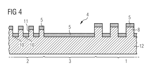
Fig. 4 shows a longitudinal section through a security element 4 that
comprises two different
sub-wavelength structures. The first sub-wavelength structure is provided in
the first surface
region 1. In the second surface region 2, a second sub-wavelength structure is
provided which
differs from the first in that the columns thereof 11 are less high and wide.
These columns 11
also periodically repeat in two directions with one period each, which in the
drawing plane can
be the same as or different from that which is perpendicular to the drawing
plane. The period of
the sub-wavelength structure of the first surface region 1 can be different
from that of the second
surface region 2. The two surface regions 1, 2 with sub-wavelength structures
are separated by
an unstructured surface region 3 without sub-wavelength structures. All three
surface regions 1-
3 are provided with the same interference coating 5.
In this manner, it is possible to convey, at different viewing angles, up to
six different color
impressions, two different color impressions each per surface region 1-3. If
the first surface
region 1 and/or the second surface region 2 are not completely covered with an
interference
coating 5, that is, in Fig. 4 for example the regions lying further to the
left or right no longer bear
an interference coating 5, two different color impressions per structured
surface region 1, 2 can
also be achieved at the same viewing angle.
However, the unstructured surface region 3 could also be omitted, so that the
first surface
region 1 and second surface region 2 are directly adjacent to one another.
Additional surface
regions, also with other sub-wavelength structures, can also be provided.
Fig. 5 shows a longitudinal section through a security element 4 that
comprises two different
sub-wavelength structures. Both sub-wavelength structures are constructed
using the same
' CA 0316.9081 2022-08-12
i
17
structure elements, namely columns 11, but in this case the columns 11, which
periodically
repeat in two directions in the plane of the security element 4, are oriented
towards a first surface
of the security element 4 in the first surface region 1 and are oriented
towards a second surface of
the security element 4 in the second surface region 2, which second surface is
opposite from the
first surface. Both surface regions 1, 2 are provided with the same
interference coating 5. The
two surface regions 1, 2 with sub-wavelength structures could also be
separated by an
unstructured surface region 3 without sub-wavelength structures.
In this embodiment, the sub-wavelength structure of the second surface region
2 corresponds to
that of Fig. 4. Here, the sub-wavelength structure of the first surface region
1 is mirrored from
that of the second surface region 2, namely over a plane that is horizontal in
this case. The
columns 11 of the first surface region 1 are in this case directed downward
and form when the
depressions in the carrier substrate 12 are filled.
Here, the plane of the top surfaces 9 of the columns 11 in the first surface
region 1 lie in the
plane of the surrounding surfaces 10 of the columns 11 in the second surface
region 1.
LIST OF REFERENCE SIGNS
1 First surface region
2 Second surface region
3 Unstructured surface region
4 Security element
5 Interference coating
6 Dielectric layer
7 Absorber layer
8 Column
9 Top surface of the column
10 Surrounding surface of the column
CA 03164081 2022-08-12
=
=
18
11 Column
12 Carrier substrate
13 Reflective layer
P Period
Effective depth