Language selection

Search

Patent 3169366 Summary

Third-party information liability

Some of the information on this Web page has been provided by external sources. The Government of Canada is not responsible for the accuracy, reliability or currency of the information supplied by external sources. Users wishing to rely upon this information should consult directly with the source of the information. Content provided by external sources is not subject to official languages, privacy and accessibility requirements.

Claims and Abstract availability

Any discrepancies in the text and image of the Claims and Abstract are due to differing posting times. Text of the Claims and Abstract are posted:

  • At the time the application is open to public inspection;
  • At the time of issue of the patent (grant).
(12) Patent Application: (11) CA 3169366
(54) English Title: FILAR ANTENNA ELEMENT DEVICES AND METHODS
(54) French Title: DISPOSITIFS ET PROCEDES POUR ELEMENT D`ANTENNE FILAIRE
Status: Report sent
Bibliographic Data
(51) International Patent Classification (IPC):
  • H01Q 1/52 (2006.01)
  • H03H 7/38 (2006.01)
  • H03H 7/46 (2006.01)
(72) Inventors :
  • EMARA, MOHAMED (Canada)
  • HAUTCOEUR, JULIEN (Canada)
  • PANTHER, GYLES (Canada)
  • BOTROS, JOSEPH (Canada)
(73) Owners :
  • TALLYSMAN WIRELESS INC. (Canada)
(71) Applicants :
  • TALLYSMAN WIRELESS INC. (Canada)
(74) Agent: PERLEY-ROBERTSON, HILL & MCDOUGALL LLP
(74) Associate agent:
(45) Issued:
(22) Filed Date: 2022-08-02
(41) Open to Public Inspection: 2024-02-02
Examination requested: 2022-08-02
Availability of licence: N/A
(25) Language of filing: English

Patent Cooperation Treaty (PCT): No

(30) Application Priority Data: None

Abstracts

English Abstract


Single band and multiband wireless antennas are an important element of
wireless systems.
Competing tradeoffs of overall footprint, performance aspects such as
impedance matching and
cost require not only consideration but become significant when multiple
antenna elements are
employed within a single antenna such as to obtain circular polarization
transmit and/or receive.
Accordingly, it would be beneficial to provide designers of a wide range of
electrical devices and
systems with compact single or multiple frequency band antennas which, in
addition to providing
the controlled radiation pattern and circular polarization purity (where
required) are impedance
matched without substantially increasing the footprint of the antenna and/or
the complexity of the
microwave / RF circuit interfaced to them, whilst supporting multiple signals
to/from multiple
antenna elements in antennas employing them. Solutions present achieve this
through provisioning
one or more capacitive series reactances discretely or in combination with one
or more shunt
capacitive reactances.


Claims

Note: Claims are shown in the official language in which they were submitted.


CLAIMS
What is claimed is:
1. A filar antenna comprising:
a plurality of first filar elements;
a plurality of second filar elements; and
a plurality of capacitive series reactances, each said capacitive series
reactance of the plurality
of series reactances connecting a feed point of an electrical circuit to which
the filar
antenna is coupled to a corresponding filar node of a plurality of filar nodes
and
effective to present a characteristic impedance at said feed point; wherein
the plurality of first filar elements each have a first electrical length
established in dependence
upon an odd multiple of a quarter wavelength of a first operating frequency;
the plurality of second filar elements each have a second electrical length,
different from the
first length, established in dependence upon an odd multiple of a quarter
wavelength of
a second operating frequency;
each of the plurality of first filar elements includes a first end and an
open, distal second end;
each of the plurality of second filar elements includes a first end and an
open, distal second
end;
each said first end of a first filar element of the plurality of first filar
elements constitutes a filar
node of the plurality of filar nodes; and
each filar node of the plurality of filar nodes is coupled to a first end of a
predetermined second
filar element of the plurality of second filar elements.
2. The filar antenna according to claim 1, wherein
the electrical circuits comprises a combining network which comprises circuit
elements
effective to constructively sum microwave electrical signals present at each
of said feed points,
each of said electrical signals having a predetermined relative phase
relationship with the
respect to the other electrical signals.
3. The filar antenna according to claim 1, wherein
each filar node of the plurality of filar nodes is either indirectly coupled
to its respective second
filar element of the plurality of second filar elements or directly coupled
via another capacitive
series reactance to its respective second filar element of the plurality of
second filar elements.

4. The filar antenna according to claim 1, wherein
each feed point of the plurality of feed points is coupled to a first filar
element of the plurality
of first filar elements via the matching circuit consisting of the capacitive
series
reactance;
the first end of each first filar element of the plurality of first filar
elements is electrically
coupled to the ground plane via a first capacitor;
the first end of each second filar element of the plurality of second filar
elements is electrically
coupled to the ground plane via a second capacitor; and
the first end of each first filar element of the plurality of first filar
elements is electrically
coupled to the first end of the second filar element of the plurality of
second filar
elements alternately arranged with the first filar element of the plurality of
first filar
elements via a third capacitor.
5. The filar antenna according to claim 1, wherein
each feed point of the plurality of feed points is coupled to a first filar
element of the plurality
of first filar elements via the matching circuit consisting of the capacitive
series
reactance;
the first end of each second filar element of the plurality of second filar
elements is electrically
coupled to the ground plane via a first capacitor; and
the first end of each first filar element of the plurality of first filar
elements is electrically
coupled to the first end of the second filar element of the plurality of
second filar
elements alternately arranged with the first filar element of the plurality of
first filar
elements via a second capacitor.
6. The filar antenna according to claim 1, wherein
each feed point of the plurality of feed points is coupled to a first filar
element of the plurality
of first filar elements via the matching circuit consisting of the capacitive
series
reactance;
the first end of each second filar element of the plurality of second filar
elements is electrically
coupled to the ground plane via a first capacitor; and
the first end of each first filar element of the plurality of first filar
elements is electrically
coupled to the first end of the second filar element of the plurality of
second filar
elements alternately arranged with the first filar element of the plurality of
first filar
elements via a second capacitor.
21

7. The filar antenna according to claim 1, wherein
each feed point of the plurality of feed points is coupled to a first filar
element of the plurality
of first filar elements via the matching circuit consisting of the capacitive
series
reactance;
the first end of each second filar element of the plurality of second filar
elements is electrically
coupled to the first end of the first filar element via a first capacitor;
the first end of each second filar element of the plurality of second filar
elements is electrically
coupled to the ground plane via a second capacitor; and
the first filar element of the plurality of first filar elements is
electromagnetically coupled to
the second filar element of the plurality of second filar elements alternately
arranged
with the first filar element of the plurality of first filar elements.
8. The filar antenna according to claim 1, wherein
each feed point of the plurality of feed points is coupled to a first filar
element of the plurality
of first filar elements via the matching circuit consisting of the capacitive
series
reactance; and
the first filar element of the plurality of first filar elements is
electromagnetically coupled to
the second filar element of the plurality of second filar elements alternately
arranged
with the first filar element of the plurality of first filar elements.
9. A filar antenna comprising:
a plurality of sets of filar antenna elements each comprising a plurality of
filar elements
arranged in a first predeternlined configuration within each set of filar
antenna elements
of the plurality of sets of filar antenna elements and in a second
predeternlined
configuration relative to the other sets of filar antenna elements; and
a plurality of capacitive series reactances; wherein
each filar element of the set of filar elements of the plurality of sets of
filar elements has an
electrical length different from an electrical length of the other filar
elements of the set
of filar elements of the plurality of sets of filar elements which is
established in
dependence upon an odd multiple of quarter wavelength of an operating
frequency of
the filar element of the plurality of filar elements, has a first end and an
open, distal
second end;
22

said first end of the first filar element within each the set of filar
elements of the plurality of
sets of filar elements constitutes a filar node of a set of filar nodes, each
of said filar
nodes further coupled to a corresponding said first end of each other filar
element of
the set of filar elements of the plurality of sets of filar elements; and
each said capacitive series reactance of the plurality of capacitive series
reactances for
connecting a filar node of the set of filar nodes to a feed point of a feed
network to
which the filar antenna is to be coupled and effective to present a
characteristic
impedance at each of said feed points.
10. The filar antenna according to claim 9, further comprising
the feed network comprising a ground plane and a combining network with a
plurality of feed
points; wherein
said combining network comprises circuit elements effective to constructively
sum microwave
electrical signals present at each of said feed points, each of said
electrical signals
having a predetermined relative phase relationship, each of said feed points
connected
to a matching circuit comprising at least one capacitive series reactance of
the plurality
of capacitive series reactances, each of said series reactances connecting one
of said
feed points to a corresponding one of said filar nodes, effective to present a

characteristic impedance at each of said feed points;
11. The filar antenna according to claim 9, wherein
each filar node of the plurality of filar nodes is directly electrically
coupled to only a first filar
element within a set of filar elements of the plurality of sets of filar
elements and indirectly
coupled to the other filar elements with the set of filar elements of the
plurality of sets of filar
elements.
12. The filar antenna according to claim 9, wherein
each feed point of the plurality of feed points is coupled to a first filar
element of a set of filar
elements of the plurality of sets of filar elements via the matching circuit
consisting of
the capacitive series reactance;
the first end of each first filar element of the set of filar elements of the
plurality of sets of filar
elements is electrically coupled to the ground plane via a first capacitor;
the first end of each subsequent filar element of the set of filar elements of
the plurality of sets
of filar elements within the predetermined configuration is electrically
coupled to a first
23

end of a preceding filar element of the set of filar elements of the plurality
of sets of
filar elements via a second capacitor; and
the first end of each other filar element of the set of filar elements of the
plurality of sets of
filar elements is electrically coupled to the ground plane via a third
capacitor.
13. The filar antenna according to claim 9, wherein
each feed point of the plurality of feed points is coupled to a first filar
element of a set of filar
elements of the plurality of sets of filar elements via the matching circuit
consisting of
the capacitive series reactance;
the first end of each subsequent filar element of the set of filar elements of
the plurality of sets
of filar elements within the predetermined configuration is electrically
coupled to a first
end of a preceding filar element of the set of filar elements of the plurality
of sets of
filar elements via a first capacitor; and
the first end of each other filar element of the set of filar elements of the
plurality of sets of
filar elements is electrically coupled to the ground plane via a second
capacitor.
14. The filar antenna according to claim 9, wherein
each feed point of the plurality of feed points is coupled to a first filar
element of a set
of filar elements of the plurality of sets of filar elements via the matching
circuit
consisting of the capacitive series reactance; and
the first end of each subsequent filar element of the set of filar elements of
the plurality
of sets of filar elements within the predetermined configuration is
electrically
coupled to a first end of a preceding filar element of the set of filar
elements of
the plurality of sets of filar elements via a first capacitor.
15. The filar antenna according to claim 9, wherein
each feed point of the plurality of feed points is coupled to a first filar
element of a set
of filar elements of the plurality of sets of filar elements via the matching
circuit
consisting of the capacitive series reactance;
the first end of each filar element of the set of filar elements of the
plurality of sets of
filar elements is electrically coupled to the ground plane via a second
capacitor;
and
each subsequent filar element of the set of filar elements of the plurality of
sets of filar
elements within the predetermined configuration is electromagnetically coupled
24

to one or more other filar elements of the set of filar elements of the
plurality of
sets of filar elements.
16. The filar antenna according to claim 9, wherein
each feed point of the plurality of feed points is coupled to a first filar
element of a set of filar
elements of the plurality of sets of filar elements via the matching circuit
consisting of
the capacitive series reactance;
the first end of each filar element of the set of filar elements of the
plurality of sets of filar
elements is electrically coupled to the ground plane via a second capacitor;
each subsequent filar element of the set of filar elements of the plurality of
sets of filar elements
within the predetermined configuration is electromagnetically coupled to one
or more
other filar elements of the set of filar elements of the plurality of sets of
filar elements.
17. A filar antenna element comprising:
a first filar antenna element comprising a first conductor of first
predetermined length, a first
predetermined width and first predetermined thickness disposed above a ground
plane;
a second filar element comprising a second conductor of second predetermined
length, a second
predetermined width and second predetermined thickness disposed above the
ground
plane and electrically coupled to the first filar antenna element; and
a first capacitor electrically coupled between a first end of the first
conductor and a feed point
for either receiving a first microwave signal to be radiated by the first
conductor or
receiving a second microwave signal from the first conductor.
18. The filar antenna according to claim 17, further comprising
a second capacitor electrically coupled between the first end of the first
conductor and the
ground plane.
19. The filar antenna according to claim 17, further comprising
a second capacitor electrically coupled between the first end of the first
conductor and a first
end of the second conductor.

20. The filar antenna according to claim 17, further comprising
a second capacitor electrically coupled between a first end of the second
conductor and the
ground plane and a third capacitor disposed between the first end of the
second conductor and
the first end of the first conductor.
21. The filar antenna according to claim 17, further comprising
a second capacitor electrically coupled between a first end of the second
conductor and the
ground plane, a third capacitor electrically coupled between the first end of
the first conductor
and the ground plane and a fourth capacitor disposed between the first end of
the second
conductor and the first end of the first conductor.
22. The filar antenna according to claim 17, wherein
the first conductor is one of a plurality of first conductors;
the second conductor is one of a plurality of second conductors;
the plurality of first conductors are either attached to a carrier or
supported by the carrier;
the plurality of second conductors are either attached to the carrier or
supported by the carrier
and
the carrier is shaped to a predetermined geometry;
the plurality of first conductors are shaped appropriately such that each
first conductor of the
plurality of first conductors traces a first helical path from the first end
of the first
conductor to a second distal end of the first conductor across the carrier;
and
the plurality of second conductors are shaped appropriately such that each
second conductor of
the plurality of second conductors traces a first helical path from the first
end of the second
conductor to a second distal end of the second conductor across the carrier.
23. The filar antenna according to claim 17, wherein
the first conductor is one of a plurality of first conductors;
the second conductor is one of a plurality of second conductors;
the first end of each first conductor is electrically coupled to a first end
of a second conductor
via a second capacitor;
the plurality of first conductors and the plurality of second conductors are
either attached to a
carrier or supported by the carrier; and
the carrier is shaped to a predetermined geometry and the plurality of first
conductors and the
plurality of second conductors are shaped appropriately such that each first
conductor
26

of the plurality of first conductors traces a first helical path from the
first end of the first
conductor to a second distal end of the first conductor across the carrier and
each second
conductor of the plurality of second conductors traces a second helical path
from the
first end of the second conductor to a second distal end of the second
conductor across
the carrier.
24. The filar antenna according to claim 23, further comprising
a plurality of third capacitors, each third capacitor electrically coupled
between a second
conductor of the plurality of second conductors and the ground plane.
25. The filar antenna according to claim 23, further comprising
a plurality of third capacitors, each third capacitor electrically coupled
between the first end of
a second conductor of the plurality of second conductors and the ground plane;
and
a plurality of fourth capacitors, each fourth capacitor electrically coupled
between the first end
of a first conductor of the plurality of first conductors and the ground
plane.
26. The filar antenna according to claim 17, further comprising
a third filar element comprising a third conductor of third predetermined
length, a third
predetermined width and third predetermined thickness disposed above the
ground
plane;
a second capacitor electrically coupled between the first end of the first
conductor and a first
end of the second conductor; and
a third capacitor electrically coupled between the first end of the second
conductor and a first
end of the third conductor.
27. The filar antenna according to claim 27, further comprising
a fourth capacitor electrically coupled between the first end of the second
conductor and the
ground plane; and
a fifth capacitor electrically coupled between the first end of the second
conductor and the
ground plane.
28. The filar antenna according to claim 27, further comprising
a fourth capacitor electrically coupled between the first end of the first
conductor and the
ground plane;
27

a fifth capacitor electrically coupled between the first end of the second
conductor and the
ground plane; and
a sixth capacitor electrically coupled between the first end of the third
conductor and the ground
plane.
29. The filar antenna according to claim 17, further comprising
a second capacitor electrically coupled between the first end of the second
conductor
and the ground plane wherein the first filar element and second filar element
are
electromagnetically coupled.
30. The filar antenna according to claim 17, further comprising
a second capacitor electrically coupled between the first end of the second
conductor and the
ground plane; and
a third capacitor electrically coupled between the first end of the first
conductor and the ground
plane; wherein
the first filar element and second filar element are electromagnetically
coupled.
31. The filar antenna according to claim 17, further comprising
a third filar element comprising a third conductor of third predetermined
length, a third
predetermined width and third predetermined thickness disposed above the
ground
plane, a second capacitor electrically coupled between a first end of the
second
conductor and the ground plane and a third capacitor electrically coupled
between a
first end of the third conductor and the ground plane, wherein the first filar
element, the
second filar element and the third filar element are electromagnetically
coupled to each
other.
32. The filar antenna according to claim 17, further comprising
a second filar element comprising a second conductor of second predetermined
length, a second
predetermined width and second predetermined thickness disposed above the
ground
plane, a third filar element comprising a third conductor of third
predetermined length,
a third predetermined width and third predetermined thickness disposed above
the
ground plane, a second capacitor electrically coupled between the first end of
the first
conductor and the ground plane, a third capacitor electrically coupled between
a first
end of the second conductor and the ground plane, and a fourth capacitor
electrically
28

coupled between a first end of the third conductor and the ground plane,
wherein the
first filar element, the second filar element and the third filar element are
electromagnetically coupled to each other.
33. An filar antenna element comprising:
a first filar antenna element comprising a first conductor of first
predetermined length, a first
predetermined width and first predetermined thickness disposed above a ground
plane;
and
a first capacitor electrically coupled between a first end of the first
conductor and a feed point
for either receiving a first microwave signal to be radiated by the first
conductor or
receiving a second microwave signal from the first conductor.
34. The filar antenna according to claim 33, further comprising
a second capacitor electrically coupled between the first end of the first
conductor and a ground
plane.
35. The filar antenna according to claim 33, further comprising
a second filar element comprising a second conductor of second predetermined
length, a second
predetermined width and second predetermined thickness disposed above the
ground
plane; and
a second capacitor electrically coupled between the first end of the first
conductor and a first
end of the second conductor.
36. The filar antenna according to claim 33, further comprising
a second filar element comprising a second conductor of second predetermined
length, a second
predetermined width and second predetermined thickness;
a second capacitor electrically coupled between a first end of the second
conductor and the
ground plane; and
a third capacitor disposed between the first end of the second conductor and
the first end of the
first conductor.
37. The filar antenna according to claim 33, further comprising
a second filar element comprising a second conductor of second predetermined
length, a second
predetermined width and second predetermined thickness;
29

a second capacitor electrically coupled between a first end of the second
conductor and the
ground plane;
a third capacitor electrically coupled between the first end of the first
conductor and the ground
plane; and
a fourth capacitor disposed between the first end of the second conductor and
the first end of
the first conductor.
38. The filar antenna according to claim 33, wherein
the first conductor is one of a plurality of first conductors;
the plurality of first conductors are either attached to a carrier or
supported by the carrier; and
the carrier is shaped to a predeterniined geometry and the plurality of first
conductors are
shaped appropriately such that each first conductor of the plurality of first
conductors
traces a first helical path from the first end of the first conductor to a
second distal end
of the first conductor across the carrier.
39. The filar antenna according to claim 33, wherein
the first conductor is one of a plurality of first conductors;
the first end of each first conductor is electrically coupled to a first end
of a second conductor
via a second capacitor;
the plurality of first conductors and the plurality of second conductors are
either attached to a
carrier or supported by the carrier; and
the carrier is shaped to a predetermined geometry and the plurality of first
conductors and the
plurality of second conductors are shaped appropriately such that each first
conductor
of the plurality of first conductors traces a first helical path from the
first end of the first
conductor to a second distal end of the first conductor across the carrier and
each second
conductor of the plurality of second conductors traces a second helical path
from the
first end of the second conductor to a second distal end of the second
conductor across
the carrier.
40. The filar antenna according to claim 39, further comprising
a plurality of third capacitors, each third capacitor electrically coupled
between a second
conductor of the plurality of second conductors and the ground plane;

41. The filar antenna according to claim 39, further comprising
a plurality of third capacitors, each third capacitor electrically coupled
between the first end of
a second conductor of the plurality of second conductors and the ground plane;
and
a plurality of fourth capacitors, each fourth capacitor electrically coupled
between the first end
of a first conductor of the plurality of first conductors and the ground
plane.
42. The filar antenna according to claim 33, further comprising
a second filar element comprising a second conductor of second predetermined
length, a second
predetermined width and second predetermined thickness disposed above the
ground
plane;
a third filar element comprising a third conductor of third predetermined
length, a third
predetermined width and third predetermined thickness disposed above the
ground
plane;
a second capacitor electrically coupled between the first end of the first
conductor and a first
end of the second conductor; and
a third capacitor electrically coupled between the first end of the second
conductor and a first
end of the third conductor.
43. The filar antenna according to claim 42, further comprising:
a fourth capacitor electrically coupled between the first end of the second
conductor and the
ground plane; and
a fifth capacitor electrically coupled between the first end of the second
conductor and the
ground plane.
44. The filar antenna according to claim 42, further comprising
a fourth capacitor electrically coupled between the first end of the first
conductor and the
ground plane;
a fifth capacitor electrically coupled between the first end of the second
conductor and the
ground plane; and
a sixth capacitor electrically coupled between the first end of the third
conductor and the ground
plane.
31

45. The filar antenna according to claim 33, further comprising
a second filar element comprising a second conductor of second predetermined
length, a second
predetermined width and second predetermined thickness disposed above the
ground
plane; and
a second capacitor electrically coupled between the first end of the second
conductor and the
ground plane; wherein
the first filar element and second filar element are electromagnetically
coupled.
46. The filar antenna according to claim 33, further comprising
a second filar element comprising a second conductor of second predetermined
length, a second
predetermined width and second predetermined thickness disposed above the
ground
plane;
a second capacitor electrically coupled between the first end of the second
conductor and the
ground plane; and
a third capacitor electrically coupled between the first end of the first
conductor and the ground
plane; wherein
the first filar element and second filar element are electromagnetically
coupled.
47. The filar antenna according to claim 33, further comprising
a second filar element comprising a second conductor of second predetermined
length, a second
predetermined width and second predetermined thickness disposed above the
ground
plane;
a third filar element comprising a third conductor of third predetermined
length, a third
predetermined width and third predetermined thickness disposed above the
ground
plane;
a second capacitor electrically coupled between a first end of the second
conductor and the
ground plane; and
a third capacitor electrically coupled between a first end of the third
conductor and the ground
plane; wherein
the first filar element, the second filar element and the third filar element
are
electromagnetically coupled to each other.
32

48. The filar antenna according to claim 33, further comprising
a second filar element comprising a second conductor of second predetermined
length, a second
predetermined width and second predetermined thickness disposed above the
ground
plane;
a third filar element comprising a third conductor of third predetermined
length, a third
predetermined width and third predetermined thickness disposed above the
ground
plane;
a second capacitor electrically coupled between the first end of the first
conductor and the
ground plane; and
a third capacitor electrically coupled between a first end of the second
conductor and the ground
plane;
a fourth capacitor electrically coupled between a first end of the third
conductor and the ground
plane; wherein
the first filar element, the second filar element and the third filar element
are
electromagnetically coupled to each other.
49. A method relating to a filar antenna element comprising:
providing a first capacitor, the first capacitor electrically coupled between
a first end of a first
conductor comprising a predetermined portion of the filar antenna element and
a feed
point of the electronic circuit for either receiving a first microwave signal
to be radiated
by the first conductor or receiving a second microwave signal from the first
conductor;
wherein
the first capacitor presents a characteristic impedance at said feed point;
and
the first conductor is disposed above a ground plane.
50. The method according to claim 49, further comprising
providing a second capacitor, the second capacitor electrically coupled
between the first end of
the first conductor and the ground plane.
51. The method according to claim 49, further comprising
providing a second capacitor electrically coupled between the first end of the
first conductor
and a first end of a second conductor comprising another predetermined portion
of the filar
antenna element.
33

52. The method according to claim 49, further comprising
providing a second capacitor electrically coupled between a first end of a
second conductor
and the ground plane; and
providing a third capacitor disposed between the first end of the second
conductor and the first
end of the first conductor; wherein
the second filar element comprises another predetermined portion of the filar
antenna element.
53. The method according to claim 49, further comprising
providing a second capacitor electrically coupled between a first end of a
second conductor
and the ground plane;
providing a third capacitor electrically coupled between the first end of the
first conductor and
the ground plane; and
providing a fourth capacitor disposed between the first end of the second
conductor and the
first end of the first conductor; wherein
the second filar element comprises another predetermined portion of the filar
antenna element.
54. The method according to claim 49, further comprising
providing a second capacitor electrically coupled between a first end of a
second conductor
and the ground plane;
providing a third capacitor electrically coupled between the first end of the
first conductor and
the ground plane; wherein
the second filar element comprises another predetermined portion of the filar
antenna element;
and
the second filar element is electromagnetically coupled to the first filar
element and therein to
said feed point.
55. The method according to claim 49, further comprising
providing a second capacitor electrically coupled between a first end of a
second conductor
and the ground plane;
providing a third capacitor electrically coupled between the first end of the
first conductor and
the ground plane; and
providing a fourth capacitor disposed between the first end of the second
conductor and the
first end of the first conductor; wherein
the second filar element comprises another predetermined portion of the filar
antenna element.
34

56. The method according to claim 49, further comprising
providing a second capacitor electrically coupled between the first end of the
first conductor
and a first end of the second conductor; and
providing a third capacitor electrically coupled between the first end of the
second conductor
and a first end of the third conductor; wherein
the second filar element comprises another predetermined portion of the filar
antenna element;
and
the third filar element comprises a further predetermined portion of the filar
antenna element.
57. The method according to claim 56, further comprising:
providing a fourth capacitor electrically coupled between the first end of the
second conductor
and the ground plane; and
providing a fifth capacitor electrically coupled between the first end of the
second conductor
and the ground plane.
58. The method according to claim 56, further comprising
providing a fourth capacitor electrically coupled between the first end of the
first conductor
and the ground plane;
providing a fifth capacitor electrically coupled between the first end of the
second conductor
and the ground plane; and
providing a sixth capacitor electrically coupled between the first end of the
third conductor and
the ground plane.
59. The method according to claim 49, further comprising
providing a second capacitor electrically coupled between a first end of a
second conductor
and the ground plane; and
providing a third capacitor electrically coupled between a first end of a
third conductor and the
ground plane; wherein
the first filar element, the second filar element and the third filar element
are
electromagnetically coupled to each other;
the second filar element comprises another predetermined portion of the filar
antenna element;
and
the third filar element comprises a further predetermined portion of the filar
antenna element.

60. The method according to claim 49, further comprising
a second filar element comprising a second conductor of second predetermined
length, a second
predetermined width and second predetermined thickness disposed above the
ground
plane;
a third filar element comprising a third conductor of third predetermined
length, a third
predetermined width and third predetermined thickness disposed above the
ground
plane;
providing a second capacitor electrically coupled between the first end of the
first conductor
and the ground plane; and
providing a third capacitor electrically coupled between a first end of a
second conductor and
the ground plane;
providing a fourth capacitor electrically coupled between a first end of the
third conductor and
the ground plane; wherein
the first filar element, the second filar element and the third filar element
are
electromagnetically coupled to each other;
the second filar element comprises another predetermined portion of the filar
antenna element;
and
the third filar element comprises a further predetermined portion of the filar
antenna element.
61. A method relating to a filar antenna element comprising:
providing a first capacitor electrically coupled between a first end of a
first conductor and a
feed point of the electrical signal for either receiving a first microwave
signal to be
radiated by the first conductor or receiving a second microwave signal from
the first
conductor; wherein
the filar antenna element comprises a first filar element and a second filar
element either
electrically couped to the first filar element or electromagnetically coupled
to the first
filar element and each of the first filar element and the second filar element
are disposed
above the ground plane.
62. The method according to claim 61, further comprising
providing a second capacitor electrically coupled between the first end of the
first conductor
and the ground plane.
36

63. The method according to claim 61, further comprising
a second capacitor electrically coupled between the first end of the first
conductor and a first
end of the second conductor.
64. The method according to claim 61, further comprising
providing a second capacitor electrically coupled between a first end of the
second conductor
and the ground plane; and
providing a third capacitor disposed between the first end of the second
conductor and the first
end of the first conductor.
65. The method according to claim 61, further comprising
providing a second capacitor electrically coupled between a first end of the
second conductor
and the ground plane;
providing a third capacitor electrically coupled between the first end of the
first conductor and
the ground plane; and
providing a fourth capacitor disposed between the first end of the second
conductor and the
first end of the first conductor.
66. The method according to claim 61, further comprising
providing a second capacitor electrically coupled between the first end of the
first conductor
and a first end of the second conductor; and
providing a third capacitor electrically coupled between the first end of the
second conductor
and a first end of a third conductor; wherein
the third filar element comprises another portion of the filar antenna
element.
67. The method according to claim 66, further comprising
providing a fourth capacitor electrically coupled between the first end of the
second conductor
and the ground plane; and
providing a fifth capacitor electrically coupled between the first end of the
second conductor
and the ground plane.
68. The method according to claim 66, further comprising
providing a fourth capacitor electrically coupled between the first end of the
first conductor
and the ground plane;
37

providing a fifth capacitor electrically coupled between the first end of the
second conductor
and the ground plane; and
providing a sixth capacitor electrically coupled between the first end of the
third conductor and
the ground plane.
69. The method according to claim 61, further comprising
providing a second capacitor electrically coupled between the first end of the
second conductor
and the ground plane wherein the first filar element and second filar element
are
electromagnetically coupled.
70. The method according to claim 61, further comprising
providing a second capacitor electrically coupled between the first end of the
second conductor
and the ground plane; and
providing a third capacitor electrically coupled between the first end of the
first conductor and
the ground plane; wherein
the first filar element and second filar element are electromagnetically
coupled.
71. The method according to claim 61, further comprising
providing a third capacitor electrically coupled between a first end of a
third conductor forming
another part of the filar antenna element and the ground plane; wherein
the first filar element and the second filar element are electromagnetically
coupled to each
other; and
the second filar element and the third filar element are electromagnetically
coupled to each
other.
72. The method according to claim 61, further comprising
a second filar element comprising a second conductor of second predetermined
length, a second
predetermined width and second predetermined thickness disposed above the
ground
plane, a third filar element comprising a third conductor of third
predetermined length,
a third predetermined width and third predetermined thickness disposed above
the
ground plane,
providing a second capacitor electrically coupled between the first end of the
first conductor
and the ground plane;
38

providing a third capacitor electrically coupled between a first end of the
second conductor and
the ground plane;
providing a fourth capacitor electrically coupled between a first end of a
third conductor and
the ground plane; and
providing a sixth capacitor electrically coupled between the first end of the
first conductor and
the first end of the second conductor; wherein
the second filar element and the third filar element are electromagnetically
coupled to each
other.
73. A method relating to a filar antenna comprising:
providing a plurality of capacitive series reactances, each said capacitive
series reactance of
the plurality of series reactances connecting a feed point of the electrical
circuit to
which the filar antenna is coupled to a corresponding filar node of a
plurality of filar
nodes of the filar antenna and effective to present a characteristic impedance
at said
feed point; wherein
the filar antenna comprises:
a plurality of first filar elements each having a first electrical length
established in
dependence upon an odd multiple of a quarter wavelength of a first operating
frequency;
a plurality of second filar elements each having a second electrical length,
different
from the first length, established in dependence upon an odd multiple of a
quarter wavelength of a second operating frequency;
each filar node of the plurality of filar nodes is a first end of a first
filar element of the plurality
of first filar elements.
74. The method according to claim 73, wherein
the electrical circuit comprises a combining network which comprises circuit
elements
effective to constructively sum microwave electrical signals present at each
of said feed points,
each of said electrical signals having a predetermined relative phase
relationship with the
respect to the other electrical signals.
39

75. The method according to claim 73, wherein
each filar node of the plurality of filar nodes is either indirectly coupled
to its respective second
filar element of the plurality of second filar elements or directly coupled
via another capacitive
series reactance to its respective second filar element of the plurality of
second filar elements.
76. The method according to claim 73, further comprising
providing a plurality of first capacitors, each first capacitor of the
plurality of first capacitors
electrically coupled between the first end of a predeterniined first filar
element of the
plurality of first filar elements and the ground plane;
providing a plurality of second capacitors, each second capacitor of the
plurality of second
capacitors electrically coupled between a first end of a predetermined second
filar
element of the plurality of second filar elements and the ground plane; and
providing a plurality of third capacitors, each third capacitor of the
plurality of third capacitors
electrically coupled between a first end of a predetermined second filar
element of the
plurality of second filar elements and a predetermined first filar element of
the plurality
of first filar elements.
77. The method according to claim 73, further comprising
providing a plurality of first capacitors, each first capacitor of the
plurality of first capacitors
electrically coupled between the first end of a predetermined second filar
element of
the plurality of second filar elements and the ground plane; and
providing a plurality of second capacitors, each second capacitor of the
plurality of second
capacitors electrically coupled between a first end of a predetermined second
filar
element of the plurality of second filar elements and a predetermined first
filar element
of the plurality of first filar elements.
78. The method according to claim 73, further comprising
providing a plurality of first capacitors, each first capacitor of the
plurality of first capacitors
electrically coupled between the first end of a predetermined second filar
element of
the plurality of second filar elements and the ground plane; and
providing a plurality of second capacitors, each second capacitor of the
plurality of second
capacitors electrically coupled between a first end of a predetermined first
filar element
of the plurality of first filar elements.

79. The method according to claim 73, wherein
each first filar element of the plurality of first filar elements is
electromagnetically coupled to
a second filar element of the plurality of second filar elements where the
plurality of
first filar elements and plurality of second filar elements are interleaved.
80. A method relating to a filar antenna comprising:
providing an electrical circuit comprising:
providing a feed network comprising a ground plane and a combining network
with a
plurality of feed points where said combining network comprises circuit
elements effective to constructively sum microwave electrical signals present
at
each of said feed points, each of said electrical signals having a
predetermined
relative phase relationship, each of said feed points connected to a matching
circuit comprising at least one capacitive series reactance of a plurality of
capacitive series reactances, each of said series reactances connecting one of

said feed points to a corresponding filar node of a plurality of filar nodes,
effective to present a characteristic impedance at each of said feed points;
and
providing the plurality of capacitive series reactances; wherein
when employed with the filar antenna each filar node of the plurality of filar
nodes is connected
to a set of filar antenna elements of a plurality of sets of filar antenna
elements; and
each said capacitive series reactance of the plurality of capacitive series
reactances connecting
a filar node of the set of filar nodes to a feed point of a feed network to
which the filar
antenna is to be coupled presents a characteristic impedance at each of said
feed points.
81. The method according to claim 80, wherein
the plurality of sets of filar antenna elements each comprise a plurality of
filar elements
arranged in a first predeterniined configuration within each set of filar
antenna elements
of the plurality of sets of filar antenna elements and in a second
predeterniined
configuration relative to the other sets of filar antenna elements;
each filar element of the set of filar elements of the plurality of sets of
filar elements has an
electrical length different from an electrical length of the other filar
elements of the set
of filar elements of the plurality of sets of filar elements which is
established in
dependence upon an odd multiple of quarter wavelength of an operating
frequency of
41

the filar element of the plurality of filar elements, has a first end and an
open, distal
second end;
said first end of the first filar element within each the set of filar
elements of the plurality of
sets of filar elements when employed with the electrical circuit is coupled to
a
predetermined filar node of a set of filar nodes and further coupled to a
corresponding
said first end of each other filar element of the set of filar elements of the
plurality of
sets of filar elements.
82. The filar antenna according to claim 80, wherein
each filar node of the plurality of filar nodes is directly electrically
coupled to only a first filar
element within a set of filar elements of the plurality of sets of filar
elements and indirectly
coupled to the other filar elements with the set of filar elements of the
plurality of sets of filar
elements.
83. The filar antenna according to claim 80, wherein
each feed point of the plurality of feed points is coupled to a first filar
element of a set of filar
elements of the plurality of sets of filar elements via the matching circuit
consisting of
the capacitive series reactance;
the first end of each first filar element of the set of filar elements of the
plurality of sets of filar
elements is electrically coupled to the ground plane via a first capacitor;
the first end of each subsequent filar element of the set of filar elements of
the plurality of sets
of filar elements within the predetermined configuration is electrically
coupled to a first
end of a preceding filar element of the set of filar elements of the plurality
of sets of
filar elements via a second capacitor; and
the first end of each other filar element of the set of filar elements of the
plurality of sets of
filar elements is electrically coupled to the ground plane via a third
capacitor.
84. The filar antenna according to claim 80, wherein
each feed point of the plurality of feed points is coupled to a first filar
element of a set of filar
elements of the plurality of sets of filar elements via the matching circuit
consisting of
the capacitive series reactance;
the first end of each subsequent filar element of the set of filar elements of
the plurality of sets
of filar elements within the predetermined configuration is electrically
coupled to a first
42

end of a preceding filar element of the set of filar elements of the plurality
of sets of
filar elements via a first capacitor; and
the first end of each other filar element of the set of filar elements of the
plurality of sets of
filar elements is electrically coupled to the ground plane via a second
capacitor.
85. The filar antenna according to claim 80, wherein
each feed point of the plurality of feed points is coupled to a first filar
element of a set of filar
elements of the plurality of sets of filar elements via the matching circuit
consisting of
the capacitive series reactance; and
the first end of each subsequent filar element of the set of filar elements of
the plurality of sets
of filar elements within the predetermined configuration is electrically
coupled to a first
end of a preceding filar element of the set of filar elements of the plurality
of sets of
filar elements via a first capacitor.
86. The filar antenna according to claim 80, wherein
each feed point of the plurality of feed points is coupled to a first filar
element of a set of filar
elements of the plurality of sets of filar elements via the matching circuit
consisting of
the capacitive series reactance;
the first end of each filar element of the set of filar elements of the
plurality of sets of filar
elements is electrically coupled to the ground plane via a second capacitor;
and
each subsequent filar element of the set of filar elements of the plurality of
sets of filar elements
within the predeternlined configuration is electromagnetically coupled to one
or more
other filar elements of the set of filar elements of the plurality of sets of
filar elements.
87. The filar antenna according to claim 80, wherein
each feed point of the plurality of feed points is coupled to a first filar
element of a set of filar
elements of the plurality of sets of filar elements via the matching circuit
consisting of
the capacitive series reactance;
the first end of each filar element of the set of filar elements of the
plurality of sets of filar
elements is electrically coupled to the ground plane via a second capacitor;
each subsequent filar element of the set of filar elements of the plurality of
sets of filar elements
within the predetermined configuration is electromagnetically coupled to one
or more other
filar elements of the set of filar elements of the plurality of sets of filar
elements.
43

Description

Note: Descriptions are shown in the official language in which they were submitted.


FILAR ANTENNA ELEMENT DEVICES AND METHODS
CROSS-REFERENCE TO RELATED APPLICATIONS
[001] This patent application claims the benefit of priority as a divisional
patent application of
Canadian Patent Application 3,079,709 filed April 27, 2020; which itself
claims the benefit of
priority from U.S. Provisional Patent 62/839,144 entitled "Filar Element
Antenna Devices and
Methods" filed April 26, 2019, the entire contents of which are incorporated
herein by reference.
FIELD OF THE INVENTION
[002] This patent application relates to antennas and more particularly to
compact single band
and multiband antennas for wireless systems such as satellite aided navigation
and mobile satellite
communications.
BACKGROUND OF THE INVENTION
[003] A global satellite navigation system (satnav) or global navigation
satellite system (GNSS)
is a system that exploits a network of autonomous geo-spatially positioned
satellites to provide
geolocation and time information to a suitable receiver anywhere on or near
the Earth where there
is an unobstructed line of sight. Whilst timing information can be obtained
from line of sight to a
single satellite geo-spatial location requires line of sight to three (at sea
level) or four satellites as
a minimum.
[004] In applications where relatively low precision is required low
complexity surface mount
patch antennas are generally employed accessing a single GNSS signal. However,
other
applications requiring high precision of timing and/or location require
accurately tuned, wider
bandwidth, antennas which, ideally, support multiple frequency operation
providing higher fidelity
reception and thereby improved multipath rejection and better output phase
linearity.
[005] Even within these applications there is a constant drive for compact
multiband antennas
that can be easily integrated into portable devices or more generally into
mobile platforms and
equipment. These antennas should provide a controlled radiation pattern,
namely a uniform
coverage of the upper hemisphere of their radiation pattern and circular
polarization purity to
improve cross-polarization rejection and hence multipath rejection.
Additionally, it is desirable for
these antennas to be electromagnetically isolated from the chassis and/or any
conductive ground
1
Date Recue/Date Received 2022-08-02

structures external to the antenna allowing for their integration into
multiple platforms with
minimal redesign.
[006] However, the overall footprint of a GNSS antenna is a combination of
both the physical
antenna itself and its associated electronics. Accordingly, a GNSS antenna is
normally deployed
together with an impedance matching circuit and either a low noise amplifier
for receivers or power
amplifier for transmitters. Where multiple antenna elements are employed to
either receive or
transmit a common signal, e.g., with four antenna elements each fed with the
common signal with
defined phase relationships for each antenna element, then a microwave circuit
such as a
quadrature splitter or combiner for example is also employed.
[007] However, with multiple antenna elements within a single antenna the
design of the
matching network can be challenging as the multiple antenna elements should be
matched
simultaneously.
[008] Accordingly, it would be beneficial to provide designers of a wide range
of electrical
devices and systems with compact multiple frequency band antennas which, in
addition to
providing the controlled radiation pattern and circular polarization purity
are impedance matched
without substantially increasing the footprint of the antenna and/or the
complexity of the
microwave / RF circuit interfaced to them which provides the multiple signals
to the multiple
antenna elements. This is achieved through provisioning one or more capacitive
series reactances
discretely or in combination with one or more shunt capacitive reactances.
[009] Other aspects and features of the present invention will become apparent
to those ordinarily
skilled in the art upon review of the following description of specific
embodiments of the invention
in conjunction with the accompanying figures.
SUMMARY OF THE INVENTION
[0010] It is an object of the present invention to mitigate limitations within
the prior art relating to
antennas and more particularly to compact single band and multiband antennas
for wireless
systems such as satellite aided navigation and mobile satellite
communications.
[0011] In accordance with an embodiment of the invention there is provided a
filar antenna
comprising:
a feeding network on a circuit board comprising a ground plane and a combining
network with a
plurality of feed points; and
2
Date Recue/Date Received 2022-08-02

a filar antenna with an equal plurality of filar nodes, wherein
said combining network comprised of circuit elements effective to
constructively sum microwave
electrical signals present at each of said feed points, each of said
electrical signals having
a predetermined relative phase relationship, each of said feed points
connected to a
matching circuit consisting of a capacitive series reactance, each of said
series reactances
connecting one of said feed points to a corresponding one of said filar nodes,
effective to
present a characteristic impedance at each of said feed points;
said filar antenna comprising a plurality of first filar elements and a
plurality of second filar
elements alternately arranged about a circumference and above the circuit
board, wherein
the plurality of first filar elements each have a first electrical length and
the plurality of
second filar elements each have a second electrical length, different from the
first length,
wherein the first electrical length of each of the plurality of first filar
antennal elements is
established in dependence upon an odd multiple of quarter wavelength of a
first operating
frequency and wherein the second electrical length of each of the plurality of
second filar
antenna elements is established in dependence upon an odd multiple a quarter
wavelength
of a second operating frequency, wherein each of the plurality of first filar
elements
includes a first end and an open, distal second end, and wherein each of the
plurality of
second filar elements includes a first end and an open, distal second end,
said first ends of
first filar elements constitutes one of said filar nodes, each of said filar
nodes further
coupled to a corresponding one of said first ends of said second filar
elements.
[0012] In accordance with an embodiment of the invention there is provided a
filar antenna
comprising:
a feeding network on a circuit board comprising a ground plane and a combining
network with a
plurality of feed points; and
a filar antenna with an equal plurality of filar nodes, wherein
said combining network comprised of circuit elements effective to
constructively sum microwave
electrical signals present at each of said feed points, each of said
electrical signals having
a predetermined relative phase relationship, each of said feed points
connected to a
matching circuit consisting of a capacitive series reactance, each of said
series reactances
connecting one of said feed points to a corresponding one of said filar nodes,
effective to
present a characteristic impedance at each of said feed points;
3
Date Recue/Date Received 2022-08-02

said filar antenna including a plurality of sets of filar antenna elements
each comprising a plurality
of filar elements arranged in a first predetermined configuration within each
set of filar
antenna elements of the plurality of sets of filar antenna elements and in a
second
predetermined configuration relative to and above the circuit board, wherein
each filar
element of the set of filar elements of the plurality of sets of filar
elements has an electrical
length different from an electrical length of the other filar elements of the
set of filar
elements of the plurality of sets of filar elements which is established in
dependence upon
an odd multiple of quarter wavelength of an operating frequency of the filar
element of the
plurality of filar elements, has a first end and an open, distal second end,
and wherein said
first end of the first filar element within each the set of filar elements of
the plurality of sets
of filar elements constitutes one of said filar nodes, each of said filar
nodes further coupled
to a corresponding said first end of each other filar element of the set of
filar elements of
the plurality of sets of filar elements.
[0013] In accordance with an embodiment of the invention there is provided a
filar antenna
element comprising:
a first filar antenna element comprising a first conductor of first
predetermined length, a first
predetermined width and first predetermined thickness disposed above a ground
plane; and
a first capacitor electrically coupled between a first end of the first
conductor and a feed point for
either receiving a first microwave signal to be radiated by the first
conductor or receiving
a second microwave signal from the first conductor.
[0014] Other aspects and features of the present invention will become
apparent to those ordinarily
skilled in the art upon review of the following description of specific
embodiments of the invention
in conjunction with the accompanying figures.
BRIEF DESCRIPTION OF THE DRAWINGS
[0015] Embodiments of the present invention will now be described, by way of
example only,
with reference to the attached Figures, wherein:
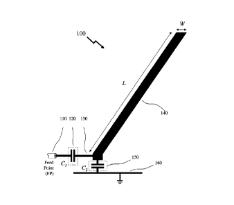
[0016] Figure 1 depicts a single filar element for a filar antenna with
capacitive series reactance
between a microwave / RF feed point and the filar element according to an
embodiment of the
invention together with a shunt capacitive reactance to ground;
4
Date Regue/Date Received 2022-08-02

[0017] Figure 2 depicts a single filar element for a filar antenna with
capacitive series reactance
between a microwave / RF feed point and the single filar element according to
an embodiment of
the invention;
[0018] Figure 3A depicts a single filar element for a filar antenna with
capacitive series reactance
between a microwave / RF feed point and the single filar element according to
an embodiment of
the invention;
[0019] Figure 3B depicts single filar elements for antennas according to
embodiments of the
invention with varying geometries employing the capacitive series reactance
between a microwave
/ RF feed point and the filar node as depicted in Figure 3A;
[0020] Figure 4 depicts a dual filar antenna element for a filar antenna with
capacitive series
reactances between a microwave / RF feed point and the filar node according to
an embodiment
of the invention together with shunt capacitive reactances to ground;
[0021] Figure 5 depicts a dual filar antenna element for a filar antenna with
capacitive series
reactances between a microwave / RF feed point and the filar node according to
an embodiment
of the invention together with a shunt capacitive reactance to ground;
[0022] Figure 6 depicts a triple filar antenna element for a filar antenna
with capacitive series
reactances between a microwave / RF feed point and the filar node according to
an embodiment
of the invention together with shunt capacitive reactances to ground;
[0023] Figure 7 depicts a dual filar antenna element for a filar antenna with
capacitive series
reactance between a microwave / RF feed point and the filar node in
conjunction with filar-to-filar
coupling according to an embodiment of the invention together with shunt
capacitive reactances
to ground;
[0024] Figure 8 depicts a triple filar antenna element for a filar antenna
with capacitive series
reactance between a microwave / RF feed point and the first filar node in
conjunction with filar-
to-filar coupling according to an embodiment of the invention together with
shunt capacitive
reactances to ground; and
[0025] Figure 9 depicts an exemplary microwave / RF circuit and antenna
employing quad dual
filar antenna elements with capacitive series reactances between the microwave
/ RF feed points
and the filar nodes according to an embodiment of the invention together with
a shunt capacitive
reactance to ground.
Date Recue/Date Received 2022-08-02

DETAILED DESCRIPTION
[0026] The present description is directed to antennas and more particularly
to compact single
band and multiband antennas for wireless systems such as satellite aided
navigation and mobile
satellite communications.
[0027] The ensuing description provides representative embodiment(s) only, and
is not intended
to limit the scope, applicability or configuration of the disclosure. Rather,
the ensuing description
of the embodiment(s) will provide those skilled in the art with an enabling
description for
implementing an embodiment or embodiments of the invention. It being
understood that various
changes can be made in the function and arrangement of elements without
departing from the spirit
and scope as set forth in the appended claims. Accordingly, an embodiment is
an example or
implementation of the inventions and not the sole implementation. Various
appearances of "one
embodiment," "an embodiment" or "some embodiments" do not necessarily all
refer to the same
embodiments. Although various features of the invention may be described in
the context of a
single embodiment, the features may also be provided separately or in any
suitable combination.
Conversely, although the invention may be described herein in the context of
separate
embodiments for clarity, the invention can also be implemented in a single
embodiment or any
combination of embodiments. Further, the terms and phrases used herein are not
intended to be
limiting, but rather, to provide an understandable description of the
invention.
[0028] Reference in the specification to "one embodiment", "an embodiment",
"some
embodiments" or "other embodiments" means that a particular feature,
structure, or characteristic
described in connection with the embodiments is included in at least one
embodiment, but not
necessarily all embodiments, of the inventions. The phraseology and
terminology employed herein
is not to be construed as limiting but is for descriptive purpose only. It is
to be understood that
where the claims or specification refer to "a" or "an" element, such reference
is not to be construed
as there being only one of that element. It is to be understood that where the
specification states
that a component feature, structure, or characteristic "may", "might", "can"
or "could" be included,
that particular component, feature, structure, or characteristic is not
required to be included.
[0029] Reference to terms such as "left", "right", "top", "bottom", "front"
and "back" are intended
for use in respect to the orientation of the particular feature, structure, or
element within the figures
depicting embodiments of the invention. It would be evident that such
directional terminology
6
Date Recue/Date Received 2022-08-02

with respect to the actual use of a device has no specific meaning as the
device can be employed
in a multiplicity of orientations by the user or users.
[0030] Reference to terms "including", "comprising", "consisting" and
grammatical variants
thereof do not preclude the addition of one or more components, features,
steps, integers or groups
thereof and that the terms are not to be construed as specifying components,
features, steps or
integers. Likewise, the phrase "consisting essentially of", and grammatical
variants thereof, when
used herein is not to be construed as excluding additional components, steps,
features integers or
groups thereof but rather that the additional features, integers, steps,
components or groups thereof
do not materially alter the basic and novel characteristics of the claimed
composition, device or
method. If the specification or claims refer to "an additional" element, that
does not preclude there
being more than one of the additional element.
[0031] A "filar element" (or filar) as used herein and throughout this
disclosure may relate to, but
not be limited to, a metallic element having a geometry of a line in that it
is long, narrow, and thin.
The term filar meaning "of or relating to a thread or line." According, a thin
film metallic trace
having a length substantially larger than its width is a linear element or
filar element.
[0032] A "filar antenna element" as used herein and throughout this disclosure
may relate to, but
not be limited to, an element of a microwave or RF antenna comprising one or
more filar elements.
[0033] A "filar antenna" as used herein and throughout this disclosure may
relate to, but not be
limited to, a microwave or RF antenna comprising one or more filar antenna
elements wherein
each of the filar antenna elements may comprise one or more filar elements.
Accordingly, a filar
antenna may, for example, comprise four filar antenna elements each comprising
a pair of filar
elements. Alternatively, it may comprise, for example, four filar antenna
elements each comprising
a single filar element or three filar elements, a single filar antenna
element, eight filar antenna
elements each comprising a pair of filar elements, or six filar antenna
elements each comprising
three filar elements. For example, Figures 1-3A and 4-8 each depict a filar
antenna element
according to an embodiment of the invention.
[0034] A "feed point" (FP) as used herein and throughout this disclosure
relates to or refers to a
point at which a filar assembly such as those depicted in Figures 1-3A and 4-8
is coupled to a
microwave circuit such as microwave feed network or microwave combining
network such as
depicted in Figure 9.
7
Date Recue/Date Received 2022-08-02

[0035] A "filar node" as used herein, and throughout this disclosure relates
to or refers to the point
at which a filar antenna element is coupled to a feed point.
[0036] According to embodiments of the present invention compact filar
antennas and filar
element based antennas are provided which employ a capacitive series reactance
between a
microwave / RF feed point and a filar node. Further, according to embodiments
of the present
invention filar element based antennas are provided which employ capacitive
series reactances
between microwave / RF feed points and filar nodes in order to provide single
band or multiband
coverage whilst being fed via a conventional microwave / RF feed point.
[0037] According to embodiments of the present invention compact filar
antennas and filar
element based antennas are provided which employ a capacitive series reactance
between a
microwave / RF feed point and a filar node in order to provide single band or
multiband coverage
whilst being fed via a conventional microwave / RF feed point. In such filar
element antennas
according to embodiments of the invention subsequent filar elements to the
initial filar element
which is coupled to the feed point via the capacitive series reactance between
the microwave / RF
feed point and the filar node are coupled through electromagnetic coupling
only to the initial filar
element.
[0038] It would be understood by one of skill in the art that filar antennas
and filar element based
antennas described with respect to embodiments of the invention and as
depicted in respect of
Figures 1 to 9 may be formed, for example, as discrete metallic elements, as
metallic elements
upon a formed or shaped circuit board, as metallic elements upon a substrate,
as metallic elements
upon a flexible circuit board, or as metallic elements formed upon a flexible
substrate.
[0039] It would be understood by one of skill in the art that filar antennas
and filar element based
antennas described with respect to embodiments of the invention and as
depicted in respect of
Figures 1 to 9 may be employed in antennas of varying three-dimensional
geometries including,
but not limited to, cylindrical, pyramidal, hemispherical, spherical, and
fructo-conical.
[0040] Accordingly, the inventors established that a filar antenna element can
be matched with a
capacitive series reactance such that the impedance characteristic of the
filar antenna element is
shifted from an intrinsic impedance to a target impedance or substantially the
target impedance,
e.g., 50E/, at the centre frequency of the frequency band of operation for the
filar antenna element.
Alternatively, the impedance may be targeted at another predetermined
impedance, if required,
such as 25E2, 75E2, 100E2 etc.
8
Date Recue/Date Received 2022-08-02

[0041] Referring to Figure 1 there is depicted a single filar antenna element
100 for a filar antenna
with capacitive series reactance between a microwave / RF feed point (FP) 110
and the filar
element 140 according to an embodiment of the invention together with a shunt
capacitive
reactance to ground. As depicted the filar element 140 of length L is coupled
at its first end to the
FP 110 via a capacitive series reactance comprising first capacitor 120 and a
track 130. The filar
element 140 has its length L established according to Equation (1) such that
its length is defined
in dependence upon an odd integer multiple of quarter wavelengths, A, at the
centre frequency of
the frequency band of operation for the filar antenna element 100 and an
offset length, Lo. Within
embodiments of the invention Lo may be negative, zero, or positive and n is
zero or a positive
integer.
L=L0+(2n+1)(i1/4) (1)
[0042] The filar element 140 having a width W and thickness T (not depicted
for clarity). The
value of the capacitive series reactance comprising the first capacitor 120,
Ci , may be established
by experimentation or through modelling and simulation. The filar element 140
in addition to being
coupled to the FP 110 via the first capacitor 120 may also be coupled to a
ground plane 160 via a
shunt capacitive reactance comprising second capacitor 150, C2. Accordingly,
the capacitive series
reactance combined with the shunt capacitive reactance to ground are effective
to transform the
impedance of the filar node to the predetermined target impedance, e.g., the
impedance at the feed-
point(FP) 110.
[0043] It would be evident that whilst the embodiments of the invention within
Figure 1 above
and Figures 2-9 described below are described with respect to filar antenna
elements comprising
one or more filar elements which are defined in terms of an odd integer
multiple of a quarter
wavelength of the wavelength at their operating frequency, see Equation (1),
these may
alternatively be defined in terms of an integer multiple of a half wavelength
of the wavelength at
their operating frequency, see Equation (2). In this instance, where defined
as an integer multiple
of the half wavelength the second end of each filar element which is open
circuit in Figures 1 to 9
would be electrically coupled either to ground or a virtual ground. Further,
within the description
reference to an operating frequency of a filar element refers to the operating
frequency of the filar
element as modified by its electromagnetic environment, e.g., a radome
protective cover, rather
than the operating frequency of a filar element discretely in air.
Accordingly, a filar element may
have its length established according to Equation (2) such that its length is
defined in dependence
9
Date Recue/Date Received 2022-08-02

upon an integer multiple of half wavelengths at the centre frequency of the
frequency band of
operation for the filar element and an offset length. As above the offset
length, Lo, may be negative,
zero, or positive and n is a positive integer.
L=Lo+n(A/2) (2)
[0044] Now referring to Figure 2 there is depicted a single filar antenna
element 200 for a filar
antenna with capacitive series reactance between a microwave / RF feed point
(FP) 210 and the
filar element 240 according to an embodiment of the invention. As depicted the
filar element 240
of length L is coupled at its first end to the FP 210 via a capacitive series
reactance comprising
first capacitor 220 and a track 230. The filar element 240 has its length L
established according to
Equation (1) such that its length is defined in dependence upon an odd
multiple of quarter
wavelengths, A, at the centre frequency of the frequency band of operation for
the filar antenna
element 100 and an offset length, Lo. The filar element 240 having a width W
and thickness T (not
depicted for clarity). The value of the capacitive series reactance comprising
the first capacitor
220, Ci , may be established by experimentation or through modelling and
simulation.
[0045] Referring to Figure 3A there is depicted a single filar antenna element
300 for a filar
antenna with capacitive series reactance between a microwave / RF feed point
(FP) 310 and the
filar element 340 according to an embodiment of the invention. As depicted the
filar element 340
of length L is coupled at its first end to the FP 310 via a capacitive series
reactance comprising
first capacitor 320 and a track 330. The filar element 340 has its length L
established according to
Equation (1) such that its length is defined in dependence upon an odd
multiple of quarter
wavelengths, A, at the centre frequency of the frequency band of operation for
the filar antenna
element 300 and an offset length, Lo. The filar element 340 having a width W
and thickness T
(not depicted for clarity). The value of the capacitive series reactance
comprising the first capacitor
320, Ci , may be established by experimentation or through modelling and
simulation.
[0046] In Figures 1-2 and Figures 4-9 the filar antennal elements are depicted
as being slanted
such that at increasing heights away from the ground plane the filar element
is also further away
from the feed point. This allows the overall height of a filar antenna
employing one or more such
slanted filar elements to be reduced in height. It would be evident to one of
skill in the art that the
slant applied to the filar elements such as depicted in Figures 1-2 and 4-9
may be varied within
different antenna designs according to the desired overall dimensions of the
antenna both in terms
of height but also length and width or diameter. It would also be evident to
one of skill in the art
Date Recue/Date Received 2022-08-02

that the slant applied to the filar elements such as depicted in Figures 1-2
and 4-9 may be reversed
such that the filar element slants in the opposite direction.
[0047] Additionally, within filar antenna elements exploiting multiple filar
elements such as
Figures 4-9 whilst these are depicted with each filar element parallel to each
other filar element
this is not a design limitation to be implied within embodiments of the
invention. Optionally, the
multiple filar elements may vary in separation with increasing height away
from the ground plane
such that within different embodiments of the invention their separations
increase with increasing
height away from the ground plane, their separations decrease with increasing
height away from
the ground plane, and some filar elements have their separations increase with
increasing height
away from the ground plane whilst other filar elements their separations
decrease with increasing
height away from the ground plane, for example.
[0048] Further, whilst the filar elements depicted in Figures 1-9 are depicted
as being linear and
of constant width (and implied constant thickness) this may not be for all
embodiments of the
invention. For example, filar elements may exhibit linear tapers in width
and/or thickness, non-
linear tapers in width and/or thickness including those defined by a
mathematical equation(s), for
example. Similarly, the filar elements may be non-linear such as those defined
by a mathematical
equation(s) or geometrical profile(s), for example. Referring to Figure 3B
there are depicted some
examples of single filar elements for antennas according to embodiments of the
invention with
varying geometries employing the capacitive series reactance between a
microwave / RF feed point
and the single filar element versus a linear uniform geometry as depicted in
Figure 3A. These
being:
= First image 300A depicting a filar element with linear taper which
decreases in width
linearly away from the ground plane;
= Second image 300B depicting a filar element with linear taper which
increases in width
linearly away from the ground plane;
= Third image 300C depicting a filar element with a curved taper which
decreases in
width along the filar element;
= Fourth image 300D depicting a filar element with a parabolic profile of
constant width
along the filar element;
= Fifth image 300E depicting a filar element with a circular profile of
constant width
along the filar element; and
11
Date Recue/Date Received 2022-08-02

= Sixth image 300F depicting a filar element with a sinusoidal profile of
constant width.
[0049] Now referring to Figure 4 there is depicted a dual filar element 400
for a filar antenna with
capacitive series reactance between a microwave / RF feed point and the filar
node according to
an embodiment of the invention combined with shunt capacitive reactances to
ground. Dual filar
element 400 comprises a first filar element 470 and a second filar element
480. First filar element
470 having a length Li, width Wi, and thickness Ti (not depicted) whilst
second filar element 480
has a length, L2, width W2, and thickness T2 (not depicted). The second filar
element 480 being
separated from the first filar element 470 by a gap .
[0050] Each of the first filar element 470 and the second filar element 480
have a first end
proximate the ground plane and electrically coupled to the feed point (FP) 410
and a second distal
end. The first end of the first filar element 470, the filar node, is coupled
to the FP 410 via track
430 and first capacitor 420, C2 and to ground 440 via second capacitor 440, C.
The first end of
the second filar element 480 is electrically coupled to the FP 410 via a third
capacitor 450, C4, the
first end of the first filar element, the track 430 and the first capacitor
420, C2. The first end of the
second filar element 480 also being electrically coupled to ground via fourth
capacitor 460, CS.
[0051] Accordingly, microwave or RF signals fed to the dual element 400 at
feed point 410 within
a first frequency band centered around fi are radiated by the first filar
element 470 which has a
length, Li, as defined by Equation (1) where the impedance of the first filar
element 470 is matched
to the target impedance via the first capacitor 420, C2, in conjunction with
the shunt capacitive
reactance from the second capacitor 440, C3. Microwave or RF signals fed to
the dual element 400
at feed 410 within a second frequency band centered around f2 are radiated by
the second filar
element 480 which has a length, L2, as defined by Equation (1) where the
impedance of the second
filar element 480 is tuned to the target impedance via the third capacitor
450, C4, in conjunction
with the shunt capacitive reactance from the fourth capacitor 460, CS,
together with the intervening
first capacitor 420, C2, and second capacitor 440, C3. For a receiver the
signals are received by the
first and second filar elements 470 and 480 respectively and coupled to the FP
410. Accordingly,
the combined capacitive series reactance(s) combined with the shunt capacitive
reactance(s) to
ground are effective to transform the impedance of each filar element, e.g.,
first filar element 470
or second filar element 480, to the predetermined target impedance, e.g., the
impedance at the
feed-point (FP) 410.
12
Date Recue/Date Received 2022-08-02

[0052] Now referring to Figure 5 there is depicted a dual filar element 500
for a filar antenna with
capacitive series reactances between a microwave / RF feed point and the filar
elements according
to an embodiment of the invention together with a shunt capacitive reactance
to ground. Dual filar
element 500 comprises first filar element 570 and second filar element 580.
First filar element 570
having a length Li, width Wi, and thickness Ti (not depicted) whilst second
filar element 580 has
a length, L2, width W2, and thickness T2 (not depicted). The second filar
element 580 being
separated from the first filar element 570 by a gap .
[0053] Each of the first filar element 570 and the second filar element 580
having a first end
proximate the ground plane and electrically coupled to the feed point (FP) 510
and a second distal
end. The first end of the first filar element 570 is coupled to the FP 510 via
track 530 and first
capacitor 520, C6. The first end of the second filar element 580 is
electrically coupled to the FP
510 via a second capacitor 540, C7, the first end of the first filar element,
the track 530 and the first
capacitor 520, C6. The first end of the second filar element 580 also being
electrically coupled to
ground via third capacitor 550, C8. Optionally, the third capacitor 550, C8,
may be omitted within
other embodiments of the invention. Alternatively, the third capacitor 550,
C8, may be omitted
within other embodiments of the invention but a shunt capacitive reactance
provided between the
first end of the first filar element and ground.
[0054] Referring to Figure 6 there is depicted a triple filar element 600 for
a filar antenna with
capacitive series reactances between a microwave / RF feed point and the filar
elements according
to an embodiment of the invention together with shunt capacitive reactances to
ground. The triple
filar element 600 comprising a first filar element 660, second filar element
670, and third filar
element 680. Accordingly, these are dimensioned as follows:
= first filar element 660 having a length Li, width Wi, and thickness Ti
(not depicted);
= second filar element 670 has a length L2, width W2, and thickness T2 (not
depicted); and
= third filar element 680 having a length L3, width W3, and thickness T3
(not depicted).
[0055] The second filar element 670 being separated from the first filar
element 660 by a gap Gi
and the third filar element 680 being separated from the second filar element
670 by a gap G2.
Typically, Ti= T2 = T3. Within Figure 6 as depicted Li >L2>L3. Alternatively,
within other
embodiments of the invention Ll<L2<L3 or Ll<L2>L3, etc.
[0056] As depicted in Figure 6 the first filar element 660 is electrically
coupled to a feed point
(FP) 610 via first capacitor 620, Cg, and track 630 whilst also being
electrically coupled to ground
13
Date Recue/Date Received 2022-08-02

690 via second capacitor 635, Cm. The second filar element 670 is electrically
coupled to the first
filar element 660 via third capacitor 640, C11, and coupled to ground 690 via
fourth capacitor 645,
C12. Similarly, the third filar element 680 is electrically coupled to the
second filar element 670
via fifth capacitor 650, C13, and coupled to ground 690 via sixth capacitor
655, C14. Optionally,
the second capacitor 635, Cm, may be omitted within other embodiments of the
invention.
Optionally, the second capacitor 635, Cm, the fourth capacitor 645, C12, and
the sixth capacitor
655, C14, may be omitted all together or in different subsets within other
embodiments of the
invention.
[0057] Now referring to Figure 7 there is depicted a dual filar element 700
for a filar antenna with
capacitive series reactance between a microwave / RF feed point and the first
filar element in
conjunction with filar-to-filar coupling according to an embodiment of the
invention together with
shunt capacitive reactances to ground. The dual filar element 700 comprising a
first filar element
760 and a second filar element 770 which are dimensioned as follows:
= first filar element 760 having a length Li, width W1, and thickness Ti
(not depicted);
and
= second filar element 770 has a length L2, width W2, and thickness T2 (not
depicted).
[0058] The second filar element 770 being separated from the first filar
element 760 by a gap Gi.
Typically, T1=T2. Within Figure 7 as depicted Li >L2. Alternatively, within
other embodiments of
the invention Li <L2.
[0059] As depicted in Figure 7 the first filar element 760 is electrically
coupled to a feed point
(FP) 710 via first capacitor 720, C15, and track 730 whilst also being
electrically coupled to ground
690 via second capacitor 740, C16. The second filar element 770 is not
electrically connected to
the first filar element 660 via a capacitor such as described and depicted in
respect of Figures 4
and 5 but is electrically coupled to ground 790 via third capacitor 750, C17.
In contrast to the direct
electrical coupling within Figures 4 and 5 the second filar element 770 is
electromagnetically
coupled to the first filar element 760.
[0060] Optionally, the third capacitor 750, C17, may be omitted. Accordingly,
the gap G1 between
the first filar element 760 and second filar element 770 in order to support
electromagnetically
coupling would be smaller than that employed in Figures 4 and 5 where the
second filar element
770 is electrically coupled via a capacitor to the first filar element.
14
Date Recue/Date Received 2022-08-02

[0061] Referring to Figure 8 there is depicted a triple filar element 800 for
a filar antenna with
capacitive series reactance between a microwave / RF feed point and the first
filar element in
conjunction with filar-to-filar coupling according to an embodiment of the
invention together with
shunt capacitive reactances to ground. The triple filar element 800 comprising
a first filar element
870, second filar element 875, and third filar element 880. Accordingly, these
are dimensioned as
follows:
= first filar element 870 having a length Li, width Wi, and thickness Ti
(not depicted);
= second filar element 875 has a length L2, width W2, and thickness T2 (not
depicted); and
= third filar element 880 having a length L3, width W3, and thickness T3
(not depicted).
[0062] The second filar element 875 being separated from the first filar
element 870 by a first gap
Gi. and the third filar element 880 being separated from the second filar
element 875 by a second
gap, Gi. Typically, Ti=T2=13.
[0063] As depicted in Figure 8 the first filar element 870 is electrically
coupled to a feed point
(FP) 810 via first capacitor 820, C18, and track 830 whilst also being
electrically coupled to ground
890 via second capacitor 840, C19. The second filar element 875 is not
electrically connected to
the first filar element 870 via a capacitor such as described and depicted in
respect of Figures 4
and 5 but is electrically coupled to ground 890 via third capacitor 850, C20.
Similarly, the third
filar element 880 is not electrically connected to the second filar element
875 via a capacitor as
depicted in respect of Figures 4 and 5 but it is electrically coupled to
ground 890 via a fourth
capacitor 860, C21. In contrast to the direct electrical coupling within
Figures 4 and 5 the second
filar element 770 is electromagnetically coupled to the first filar element
870 whilst the third filar
element 880 is electromagnetically coupled to the first filar element 870
directly or indirectly via
the second filar element 875.
[0064] Optionally, the third capacitor 850, C20, and/or the fourth capacitor
860, C21, may be
omitted. Accordingly, the gaps Gi and G2 between the first filar element 870
and second filar
element 875 and third filar element 875 and second filar element 875
respectively in order to
support electromagnetically coupling would be smaller than that employed in
Figures 4 and 5
where the second filar element 875 and third filar element 880 are
electrically coupled via
capacitors to the first filar element.
[0065] Now referring to Figure 9 there is depicted a schematic 900 of an
exemplary microwave /
RF circuit and antenna employing four dual filar elements with capacitive
series reactances
Date Recue/Date Received 2022-08-02

between the microwave / RF feed points and the filar nodes according to an
embodiment of the
invention together with a shunt capacitive reactance to ground. Accordingly,
within schematic 900
are depicted first to fourth filar antenna elements 900A to 900D respectively
which are depicted
as being of similar design to that depicted in Figure 5 with capacitive series
reactance between the
first to fourth feed points (FPs) 950A to 950D respectively and the respective
first to fourth filar
antenna elements 900A to 900D. Accordingly, first to fourth FPs 950A to 950D
respectively may
be a connection to a microwave feed circuit or microwave combiner circuit such
as through
discrete microwave or RF cables or a circuit board for example. First and
second filar antenna
elements 900A and 900B are coupled via first and second FPs 950A and 950B
respectively to first
hybrid coupler 930. Third and fourth filar antenna elements 900C and 900D are
coupled via third
and fourth FPs 950C and 950D respectively to second hybrid coupler 940.
[0066] A first output of the first hybrid coupler 930 is coupled to Balun 920
whilst a second output
of the first hybrid coupler 930 is terminated with a load resistance. A first
output of the second
hybrid coupler 940 is coupled to Balun 920 whilst a second output of the
second hybrid coupler
940 is terminated with a load resistance. Similarly, a first output of the
Balun 920 is coupled to an
output port whilst a second output of the Balun 920 is optionally terminated
in a load resistance.
Accordingly, considering a filar antenna employing first to fourth antenna
elements 900A to 900D
respectively formed upon a flexible circuit board or carrier and wound into a
cylinder then these
receive couple four sets of received microwave / RF signals which are combined
through the first
and second hybrid couplers 930 and 940 and Balun 920 to generate an output
signal at the output
port 910. Where the microwave / RF signals have relative phases received by
the first to fourth
antenna elements have a relative phase difference sequentially of 0 , 90 , 180
, and 270 then
these signals are initially combined within each of first and second hybrid
couplers 930 and 940
and then within the Balun 920 to generate an output signal. The output ports
of the first and second
hybrid couplers 930 and 940 being those summing the inputs whilst the other
output ports
terminated with load resistors represent the ports yielding the difference
between the two inputs.
Alternatively, the reverse scenario results in an input signal coupled to the
Balun 920 being initially
split into two signals 180 out of phase with respect to one another which are
then coupled to the
first and second hybrid couplers 930 and 940 respectively which each generate
a pair of signals
with 90 relative phase such that the circuit provides four output signals at
relative phase difference
sequentially of 0 , 90 , 180 , and 270 which are then radiated by the first
to fourth antenna
16
Date Recue/Date Received 2022-08-02

elements 900A to 900D respectively combining to generate a circularly
polarized signal from the
antenna. Accordingly, when employed as a receiver the antenna receives
circularly polarized
signals. Embodiments of the invention according to the sequence of phases
implemented may
operate to receive and/or transmit left hand circularly polarized signals or
right hand polarized
signals. Optionally, within other embodiments of the invention the Balun 920
may be a
transformer.
[0067] Within Figures 1 to 9 the filar antenna elements and antennas employing
them exploit one
or more filar elements which are coupled to a feed point and are disposed
relative to a ground plane
without or without capacitors disposed between all or some of the filar
elements and the ground
plane. Within embodiments of the invention this ground plane may be formed,
for example, on
one side of or upon a layer of a printed circuit board or electronic circuit,
flexible PCB, or an
equivalent, hereinafter referred to as a PCB for ease of reference. Within
embodiments of the
invention the filar elements are mechanically and/or electrically coupled to
the other side of the
PCB to that on which the ground plane is formed or upon a side of the PCB when
the ground plane
is formed by a layer within the PCB. Accordingly, the PCB may be a single or
multi-layer circuit
providing contacts for electrical attachment of each of the filar antenna
elements and therein the
individual filar elements. Further, the PCB may support either integrated
within it or attached to it
capacitors to provide the capacitive series reactance from the feed points to
the first filar elements
as well as , optionally, the capacitors disposed between the filar elements
where multiple filar
elements are employed and capacitors coupling filar elements to the ground
plane.
[0068] Accordingly, with respect to Figure 9 a microwave receiver and/or
microwave transmitter
can be coupled to the microwave quadrature feed network through the port. The
four feed points
feed nodes are connected to the four filar nodes of the filar antenna elements
described above
wherein these may be spatially located on a former, such as a PCB
implementation of the feed
network such that phase increases uniformly (e.g., in 90 steps) as a function
of position (described
by azimuth angle) around the printed circuit board and the feed network
provides equal amplitude
signals to the four antenna coupling terminals. Each of the filar antenna
elements, whether a single
filar element based for a single frequency band or multiple filar element
based for multiple
frequency band operation may exploit a former such as the plastic carrier of a
flexible microwave
circuit for example allowing the four elements to be formed upon a single
former providing ease
17
Date Recue/Date Received 2022-08-02

of handling, enhanced material considerations etc. This former may be formed
into the cylinder
for example.
[0069] Within other embodiments of the invention the former may be designed
and formed to
provide four antennas evenly distributed around the periphery of a
hemispherical surface and form
the antennas across this hemispherical surface. Within other embodiments of
the invention the
former may be designed and formed to provide the four antennas evenly
distributed around the
surface of a spherical surface and form the antennas across this spherical
surface. Within other
embodiments of the invention the former may be designed and formed to provide
the four antennas
evenly distributed around the periphery of a frusto-conical surface and form
the antennas across
this frusto-conical surface. Within other embodiments of the invention the
former may be designed
and formed to provide the four antennas evenly distributed around the
periphery of a polygonal
surface and form the antennas across this polygonal surface. Such a polygonal
surface may have
4, 5, 6, 7, 8, etc. sides or other numbers although typically more sides yield
lower angular
transitions and hence induced stress and/or fatigue.
[0070] Within the embodiments of the invention described and depicted above in
respect of
Figures 7 to 8 the capacitors for the other filar elements electromagnetically
coupled to the first
filar element with the electrical feed have been described and depicted as
being at the same end of
the overall antenna construction as the capacitor attached to that first filar
element. However, in
other embodiments of the invention the electrical connection(s) to the other
capacitors may be
disposed at either end of their respective filar elements as appropriate for
the overall construction,
footprint, performance etc.
[0071] Within the embodiments of the invention described and depicted above in
respect of
Figures 1 to 8 the capacitors, such as those providing the capacitive series
reactance between the
first filar element and the feed points, are depicted as connecting to the
filar elements at a first end,
this being the end closest to the ground plane. However, within other
embodiments these
connections between filar elements and capacitors may be implemented towards
the end of the
filar elements closest to the ground plane rather than at the end.
[0072] It would be evident to one of skill in the art that the filar elements
are electrical conductors
(conductors) formed from a suitable conductive material or combination of
conductive materials
in alloy and/or layered form. Such conductive materials may include, but not
be limited to, copper,
gold, silver, aluminum, titanium, tungsten, platinum, palladium, and zinc.
18
Date Recue/Date Received 2022-08-02

[0073] Specific details are given in the above description to provide a
thorough understanding of
the embodiments. However, it is understood that the embodiments may be
practiced without these
specific details. For example, circuits may be shown in block diagrams in
order not to obscure the
embodiments in unnecessary detail. In other instances, well-known circuits,
processes, algorithms,
structures, and techniques may be shown without unnecessary detail in order to
avoid obscuring
the embodiments.
[0074] The foregoing disclosure of the exemplary embodiments of the present
invention has been
presented for purposes of illustration and description. It is not intended to
be exhaustive or to limit
the invention to the precise forms disclosed. Many variations and
modifications of the
embodiments described herein will be apparent to one of ordinary skill in the
art in light of the
above disclosure. The scope of the invention is to be defined only by the
claims appended hereto,
and by their equivalents.
[0075] Further, in describing representative embodiments of the present
invention, the
specification may have presented the method and/or process of the present
invention as a particular
sequence of steps. However, to the extent that the method or process does not
rely on the particular
order of steps set forth herein, the method or process should not be limited
to the particular
sequence of steps described. As one of ordinary skill in the art would
appreciate, other sequences
of steps may be possible. Therefore, the particular order of the steps set
forth in the specification
should not be construed as limitations on the claims. In addition, the claims
directed to the method
and/or process of the present invention should not be limited to the
performance of their steps in
the order written, and one skilled in the art can readily appreciate that the
sequences may be varied
and still remain within the spirit and scope of the present invention.
19
Date Recue/Date Received 2022-08-02

Representative Drawing
A single figure which represents the drawing illustrating the invention.
Administrative Status

For a clearer understanding of the status of the application/patent presented on this page, the site Disclaimer , as well as the definitions for Patent , Administrative Status , Maintenance Fee  and Payment History  should be consulted.

Administrative Status

Title Date
Forecasted Issue Date Unavailable
(22) Filed 2022-08-02
Examination Requested 2022-08-02
(41) Open to Public Inspection 2024-02-02

Abandonment History

Abandonment Date Reason Reinstatement Date
2024-03-11 R86(2) - Failure to Respond

Maintenance Fee

Last Payment of $100.00 was received on 2022-08-02


 Upcoming maintenance fee amounts

Description Date Amount
Next Payment if small entity fee 2025-08-05 $50.00
Next Payment if standard fee 2025-08-05 $125.00

Note : If the full payment has not been received on or before the date indicated, a further fee may be required which may be one of the following

  • the reinstatement fee;
  • the late payment fee; or
  • additional fee to reverse deemed expiry.

Patent fees are adjusted on the 1st of January every year. The amounts above are the current amounts if received by December 31 of the current year.
Please refer to the CIPO Patent Fees web page to see all current fee amounts.

Payment History

Fee Type Anniversary Year Due Date Amount Paid Paid Date
Application Fee 2022-08-02 $407.18 2022-08-02
Maintenance Fee - Application - New Act 2 2024-08-02 $100.00 2022-08-02
Request for Examination 2026-08-04 $814.37 2022-08-02
Owners on Record

Note: Records showing the ownership history in alphabetical order.

Current Owners on Record
TALLYSMAN WIRELESS INC.
Past Owners on Record
None
Past Owners that do not appear in the "Owners on Record" listing will appear in other documentation within the application.
Documents

To view selected files, please enter reCAPTCHA code :


To view images, click a link in the Document Description column. To download the documents, select one or more checkboxes in the first column and then click the "Download Selected in PDF format (Zip Archive)" or the "Download Selected as Single PDF" button.

List of published and non-published patent-specific documents on the CPD .

If you have any difficulty accessing content, you can call the Client Service Centre at 1-866-997-1936 or send them an e-mail at CIPO Client Service Centre.


Document
Description 
Date
(yyyy-mm-dd) 
Number of pages   Size of Image (KB) 
New Application 2022-08-02 4 113
Abstract 2022-08-02 1 31
Description 2022-08-02 19 1,349
Claims 2022-08-02 24 1,279
Drawings 2022-08-02 10 118
Office Letter 2022-08-31 3 293
Non-compliance - Incomplete App 2022-08-31 2 223
Compliance Correspondence 2022-09-01 6 191
New Application 2022-08-02 6 306
Prosecution Correspondence 2022-10-17 12 487
Office Letter 2023-01-04 2 210
Representative Drawing 2023-12-14 1 3
Cover Page 2023-12-14 1 40
Examiner Requisition 2023-11-10 7 369