Note: Descriptions are shown in the official language in which they were submitted.
CA 03169871 2022-08-02
WO 2021/156844
PCT/IB2021/051007
MICROFLUIDIC DEVICE WITH INTERFACE PINNING REACTION VESSELS WITHIN A
FLOW-THROUGH CHAMBER, KIT FOR FORMING, AND USE OF, SAME
Field of the Invention
[0001] The present invention relates in general to microfluidic devices for
multiplex
assays, and in particular to a microfluidic chip with multiple interface
pinning reaction
vessels for concentrating and arraying bound targets/analytes in respective
regions of a
flow-through chamber.
Background of the Invention
[0002] Multiplex assays are important for a wide variety of testing and
studies in
biological sciences, pharmacology, food and water testing, and clinically.
Particularly
useful are systems that allow for a test sample to be tested for presence of a
few to many
species (e.g., up to 384 for standard well plates) with the test sample
provided to a plurality
of target regions in sequence as in a flow through chamber, as opposed to
dividing the test
sample and sending each fraction to a different target region. Flow-through
processing
allows for a more parsimonious use of the test sample, and is particularly
required when
low volumes of test samples are available.
[0003] Historically, multiplex assays have mostly been done using well
plates and have
required intensive human intervention, or expensive robotic manipulators. The
use of
standard well plates offers limited potential for miniaturization, as a volume
and spacing of
the well plate needed for read-out and pipetting (while avoiding cross-
contamination risks)
limit the well plates to a certain size and volume of liquid.
[0004] A critical step in multiplex assays is read-out. Once targets are
bound to capture
moieties in respective wells, it is desired to inspect the regions to
determine the presence
of the target from the sample. This is why it is important for wells to
concentrate and
spatially array the bound targets/analytes. A density of bound targets when
inspected from
a predefined vantage is essential for easy, reliable, low-cost, inspection.
For example, the
bound targets may be fluorescently labelled or dyed for visual read out, or
other read out
technologies could be used.
[0005] Colorimetric assays are widely used as diagnostic tools for
detecting target
analyte through the formation of a colored reaction product. They are commonly
performed
using standard (e.g., 96 well) well plates (e.g., made of polystyrene) where
capture probes
are immobilized at the bottom of each well. Solutions are pipetted in and out
of the wells
1
CA 03169871 2022-08-02
WO 2021/156844
PCT/IB2021/051007
to expose the probes to i) a sample, possibly or certainly containing analyte,
ii) conjugated
detection antibody (e.g., conjugated with HRP), and iii) developing agent
(e.g., TMB) as
well as iv) rinse buffer to perform wash steps in between. Although the
colorimetric reaction
happens at the interface (where probe-analyte conjugate is located), the
forming product
typically dissipates in solution. Colorimetric assays generally benefit from
automation for
high-volume test runs. Read-out is accomplished through imaging (photographic
analysis,
absorbance spectra) for each well.
[0006] Test strips can be used alternatively to well plates. These can
reduce a volume
of the sample liquid, and still provide good read-out capabilities with well
selected
visualization reagents. These typically use capillary effect to draw sample
liquid from an
input area into contact with one or more probe areas. However, there are
challenges with
manipulating small volumes of liquids, and avoiding cross-contamination. It
can be difficult
to supply a same small volume to different regions for multiplex assay when
capillarity is
the sole driver of the liquid, and reliable operation generally calls for an
oversupply of liquids
to ensure that the liquid covers the test strip. Test strips often need
handling procedures
to avoid contact with sensitive regions prior to use. A range of binding
assays are limited
as many-step processes (e.g. sample supply, wash, antibody conjugate delivery,
wash,
developer delivery and wash) are substantially precluded, even though these
many-step
processes may be more reliable. Finally, if sample prep is required, complex
equipment
may be called for that largely vitiate the portability, and efficiency
advantages of test strips.
[0007] Paper, for example, has become another popular and widely used
support for
colorimetric tests (A. W. Martinez, S. T. Phillips, M. J. Butte, G. M.
Whitesides "Patterned
paper as a platform for inexpensive, low-volume, portable bioassays" Angew.
Chem. Int.
Ed. 2007, 46, 1318, Morbioli et al. "Technical aspects and challenges of
colorimetric
detection with microfluidic paper-based analytical devices (pPADs) ¨ a review"
Anal. Chim.
Acta 2017, 970, 1, Gong & Sinton "Turning the page: advancing paper-based
microfluidics
for broad diagnostic application" Chem. Rev. 2017, 117, 8447). Paper can be
implemented
either in the form of a continuous test strip that contains multiple probes
immobilized with
spatial control, or as isolated segments each of which having been modified
with a
respective probe. It is possible to structure paper using wax or resin in
order to provide
guidance and directionality to flowing liquid (Martinez et al. 2007).
[0008] There are many patents on test strips (e.g. US 4,361,537, US
4,960,691, US
4,168,146, CA 2493616, CA 2375034), including CA 2637974 and CA 2272260 which
teach multiple analyte binding assays. Test strips typically offer open
structures for
conducting the sample liquid between various reaction and (sometimes distinct)
read-out
2
CA 03169871 2022-08-02
WO 2021/156844
PCT/IB2021/051007
zones, under the influence of capillary action. W003/012443 to Chan teaches a
paper-
based membrane (test strip) for a rapid diagnostic device in which a liquid
test sample is
assayed to detect a target analyte. Chan teaches that porosity of the membrane
has a
large influence on flow rate through the membrane, and sensitivity of the
assay. The larger
the pore size, 1- the faster the flow rate (and the shorter the interaction
time), and 2- the
less the surface area of the receptor molecules. Both of these tend to
decrease sensitivity
ceteris paribus.
[0009] The use of plastic based, microfluidic systems for multiplex assay
holds great
potential for developing point-of-care technology. However, incorporation of
these
detection schemes into microfluidic devices remains challenging, mainly
because current
microfluidic systems lack the capacity (reservoir depth) and target density at
the same time,
both of which are required in order to supply reagents for development and to
ensure
accumulation of colored reaction product for providing strong, measurable
signals.
Microfluidic chips are generally produced by relief patterning of a surface of
a film to define
a network of chambers and channels, and then covering this surface with a lid
to enclose
the chambers and channels. This does not usually permit deep reservoirs as are
used
routinely in well plates. Furthermore, flow of solution (as it occurs in
microfluidic systems)
generally leads to dissipation of reaction product and is therefore
detrimental to detection,
which is not a problem if separate well plates are used. It is a challenge for
microfluidic
devices to provide readable regions with the depth limitations, and to provide
flow-through
chambers while, at the same time, retaining colorimetric products within the
regions.
[0010] One prevailing strategy to circumvent the problems of dissipation
and limited
depth, is the use of porous materials that can act as a three-dimensional
reaction matrix.
For example, an assay has been demonstrated as a Health Canada-approved method
for
the detection of enterohemorrhagic E. coli (EHEC) colony isolates on a cloth
substrate (B.
Blais et al. In: Compendium of Analytical Methods 2013, Vol. 3. Laboratory
Procedures of
Microbiological Analysis of Foods, MFLP-22). Key marker genes for this
organism (eae,
rtb0157, vt1, vt2 etc.), amplified in a multiplex PCR process, incorporate a
detectable
digoxigenin (DIG) label, which is revealed in an immunoenzymatic process using
TMB
conversion after hybridization with target-specific oligonucleotide capture
probes (A.
Martinez-Perez and B. W. Blais "Cloth-based hybridization array system for the
identification of Escherichia coli 0157:H7" Food Control 2010, 21, 1354).
Applicant has
demonstrated a colorimetric detection assay for pathogenic E. coli by
integrating a
polyester cloth substrate on a microfluidic chip (M. Geissler, L. Clime, X. D.
Hoa, K. J.
Morton, H. Hebert, L. Poncelet, M. Mounier, M. Deschenes, M. E. Gauthier, G.
Huszczyn-
3
CA 03169871 2022-08-02
WO 2021/156844
PCT/IB2021/051007
ski, N. Co rneau, B. W. Blais, T. Veres "Microfluidic integration of a cloth-
based hybridization
array system (CHAS) for rapid, colorimetric detection of enterohemorrhagic
Escherichia
coli (EHEC) using an articulated, centrifugal platform" Anal. Chem. 2015, 87,
10565).
[0011] The
integration of paper or cloth (fabric) in a microfluidic chip complicates chip
design, fabrication and assembly, and therefore adds to the cost per assay.
Surface
modification of cloth or paper to localize capture probes requires processing
that is not
compatible with low-cost fabrication schemes unless a very large production
run is
envisaged. Integration of separate, small swatches of fabric into a
microfluidic chip with a
required alignment precision, is generally time-consuming and expensive.
Bonding and
functionalization of the swatches also add substantial costs to the process.
[0012] Another
approach is to define a 3D scaffold with a gel-type structure. For
example, US 2011/0186165 to Borenstein (165) uses hot embossing of
thermoplastic films
to form microfluidic channels and chambers, and then injects a gel matrix, in
at least one
chamber between two channels. Unfortunately, supplying and affixing gels, can
be a
laborious and capricious exercise (see [0049]-[0050]). The gel may have
porosity,
permeability or surface wetting properties that change with time, and are
liable to a host of
stability issues that may make their non-immediate use unreliable. As gels are
essentially
random arrays of very fine structural members, they have very high surface
area for
interacting with a liquid, which is good for assay efficiency, but are very
difficult to wash
between steps, and they are prone to clogging or blocking. Furthermore gels
may not have
a desired reference surface contrast, and may absorb or block light from some
reporter
molecules, thereby limiting detection alternatives.
[0013] '165
refers to microfluidic devices with "non-uniformly treated and/or patterned
interior surfaces". Surface treatment and/or patterning is said to include
chemical and/or
topographical surface modifications; the chemical modification to include
treatments and/or
coatings with inorganic or organic (e.g. antibodies or proteins) substances.
The interior
surface of a microfluidic device includes the walls of the microchannels and
walls of the
gel-holding chamber. Note these features on interior surfaces are not
themselves said to
alter fluid dynamics, and once filled with gel, the porosity of the gel would
substantially
determine fluid conductance. Patterning implies repetitive (though not
necessarily perfectly
regular) surface modifications. For example, in some embodiments, one or more
microchannel walls feature chemically (including, e.g., biologically) treated
islands, or non-
treated islands on an otherwise treated wall. Certain
interior surfaces may be
topographically structured, e.g., with microposts. According to '165,
microposts disposed
4
CA 03169871 2022-08-02
WO 2021/156844
PCT/IB2021/051007
at the top and bottom surfaces of a gel-containing chamber may serve to hold
the gel in
place or to support cells, or stiffen walls to improve cell adhesion.
[0014] Apart from '165, which teaches the use of posts for cell support,
and to confine
gel, there is a great deal of knowledge in the art surrounding arrays of posts
or like features
in microfluidic chips. While US 6,210,986 to Arnold et al. (986) seems to be
committed to
using ceramic and glass substrates, '986 teaches etched microfluidic
structures with an
array of posts within a microfluidic channel used as flow guides, material
supports, or as
the porous phase for chromatographic separation. Pillar arrays are also known
for: 1-force
measurements (J. C. Doll et al. "SU-8 force sensing pillar arrays for
biological
measurements" Lab Chip 2009, 9, 1449) and cell mechanics studies (S. Ghassemi
et al.
"Fabrication of elastomer pillar arrays with modulated stiffness for cellular
force
measurements" J. Vac. Sci. Technol. B 2008, 26, 2549); 2- surface-enhanced
Raman
scattering - if the pillars are metallized and nano-scale (e.g. Applicant's WO
2012/122628
entitled "Microfluidic system having monolithing plasmonic nanostructures"; Y.
Q. Wang et
al. "Size-dependent SERS detection of R6G by silver nanoparticles immersion-
plated on
silicon nanoporous pillar array" Appl. Surf. Sci. 2012, 258, 5881; and J. C.
Caldwell et al.
"Plasmonic nanopillar arrays for large-area, high-enhancement surface-enhanced
Raman
scattering sensors" ACS Nano 2011, 5,4046); 3-particle separation based on
Deterministic
Lateral Displacement, if the pillars have a prescribed layout and dimensions
relative to the
fluid and particles (e.g. L. R. Huang et al. "Continuous particle separation
through
deterministic lateral displacement" Science 2004, 304, 987; D. W. Inglis et
al. "Critical
particle size for fractionation by deterministic lateral displacement" Lab
Chip 2006, 6, 655;
and J. McGrath et al. "Deterministic lateral displacement for particle
separation: a review"
Lab Chip 2014, 14, 4139); 4- immunomagnetic capture, if the pillars are coated
and
magnetized (e.g. L. Malic et al. PCT/1132019/056616, and L. Malic et al.
"Polymer-based
microfluidic chip for rapid and efficient immunomagnetic capture and release
of Listeria
monocytogenes" Lab Chip 2015, 15, 3994); 5-creating passive pumping elements
/wicking
to displace liquid in a microfluidic channel (e.g. M. Zimmermann et al.
"Capillary pumps for
autonomous capillary systems" Lab Chip 2007, 7, 119, and L. Gervais and E.
Delamarche
"Toward one-step point-of-care immunodiagnostics using capillary-driven
microfluidics and
PDMS substrates" Lab Chip 2009, 9, 3330); and 6- controlling interface
adhesion in
microfluidic blister seals (e.g. M. Janta et al. "Patterned film for forming
fluid-filled blister,
microfluidic blister, and kit and method of forming" US 2017/0291747) and
valves (J.-C.
Galas et al. "Semipermanently closed microfluidic valve" U59435490).
CA 03169871 2022-08-02
WO 2021/156844
PCT/IB2021/051007
[0015] While it might appear obvious to place a test strip into a suitably
sized cavity of
a microfluidic chip to provide all the advantages of the test strip in terms
of liquid control
and read-out, and freedom from handling restrictions (once installed): 1-test
strips are only
designed for a narrow range of test protocols, and microfluidics can permit a
broader range
that includes some protocols that are better suited to some tests; 2- the
costs of test strips
are simply added to the costs of the microfluidic chip (with costs for
assembly); 3- read-out
of the test strip through the microfluidic chip might be more difficult; and 4-
bonding and
sealing of chips may be made more difficult by the inclusions as it is for
fabric swatches.
[0016] Accordingly there is a need for a microfluidic chip adapted for
multiplex assays
that provides flow control and high density of targets without relying on
exogenous scaffolds
or materials inserted into the chip.
Summary of the Invention
[0017] Applicant has devised a flow-through chip that: can be easily
functionalized to
provide a plurality of probes in respective regions with low risk of cross-
contamination; has
high surface area for the probes in each region, for improved assay efficiency
and read-out
of minuscule volumes; is integrated with a microfluidic chip; and allows for
long shelf-life
usage. The microfluidic chip structure allows for enclosed testing spaces that
have reduced
handling limitations, and allows for a wide range of assay processes,
including colorimetric
or developer-based assays. The microfluidic chip structure enables lower
volume assays
with good readout because of a high surface area within interface-pinning
reaction vessels
that allow for high target density.
[0018] Accordingly a kit for forming a microfluidic chip is provided, the
kit comprising a
substrate having a surface with topographical relief bearing at least 4 relief
patterned
regions, each defining a respective interface-pinning reaction vessel covering
a footprint
area of less than 15 cm2; and a part with a covering surface dimensioned for
sealing against
the substrate to cover the substrate to enclose at least a single flow-through
chamber that
includes the vessels.
[0019] Each region may preferably extend 0.1 to 50 mm in both planar
directions, and
may have a surface area that is at least 1.2 times, and more preferably 1.6
times, or 2-50
times its footprint area. Each region may be separated from each neighbouring
region by
segments of the surface that have a ratio of surface area to footprint that is
no more than
1.1. Each segment may separate the neighbouring regions by a distance that is
greater
than: 0.1 mm; or 5% of a mean of the extents of the neighbouring regions in
the planar
6
CA 03169871 2022-08-02
WO 2021/156844
PCT/IB2021/051007
directions. As such each region is an interface-pinning reaction vessel for
many fluids,
separated from other regions to both avoid cross-contamination, and to
facilitate readout.
[0020] The chamber may have at least one ingress from a microfluidic
network of the
chip formed by the kit, the microfluidic network comprising at least two
microfluidic channels
coupling two different reservoirs with the ingress. The microfluidic network
may comprise
two subnetworks: a marking network equipped for performing a marking process
within the
chamber; and a prep network equipped for treating a test sample.
[0021] The part may be a first film, and the covering surface, a side of
the first film. The
side of the first film, or the substrate surface, may be relief patterned to
define one or more
of: one side of the chamber, the relief-patterned regions, one side of the
ingress, the whole
ingress defined as a through-bore of the first film, and at least part of the
microfluidic
network. The relief pattern may define at least one microfluidic blister for
retaining a liquid.
[0022] The substrate may be in the form of a second film; the kit further
comprises a
third film; and at least one of the first, second or third films, has at least
one through-bore
via for coupling two microfluidic networks when the films are stacked and
bonded.
[0023] At least one of the substrate and the part is preferably transparent
to inspection
at a wavelength, and a chip produced by sealing the surface and the covering
surface (and
possibly other steps) permits inspection of the vessels through the
transparent material.
Preferably the transparent material is sealed to a material that is reflective
or opaque to the
inspection wavelength, to improve imaging of the vessels.
[0024] The kit may further comprise supplies of at least 3 probes. The
probes may be
supplied by functionalizing each of the vessels with a respective one and only
one of the at
least 3 probes.
[0025] The substrate may be composed of a cyclic olefin copolymer-,
polystyrene-, or
polylactic acid-based polymer and the functionalization may be consistent with
formation
by oxygen plasma surface activation or UV/ozone surface activation. Prompt
reaction with
cyanogen bromide, or silanes (aldehyde, epoxy, or amine in conjunction with
gluteraldehyde) and binding of the probe.
[0026] The probe may be supplied (for example prior to assembly of the
chip), carried
by a liquid in a fluid-tight container, the liquid having a contact angle and
viscosity allowing
for spontaneous spreading of the liquid across the region, and a volume
sufficient to cover
7
CA 03169871 2022-08-02
WO 2021/156844
PCT/IB2021/051007
the region, but insufficient volume to overcome interface pinning, whereby the
liquid, if it
meets any part of the region, is self-limited to substantially covering that
region.
[0027] The kit may further comprise at least one marking liquid, such as
one or more
of: a developer; a conjugated detection antibody with a target-specific
binding moiety; a
wash buffer; a hybridization solution; formaldehyde; and a PCR product
contained within a
microfluidic chamber of a chip formed with at least the substrate and the
cover. If the
substrate is a cyclic olefin copolymer, the developer may be 3,3',5,5'-
tetramethylbenzidine.
[0028] The kit may be assembled to form the chip. The chip may be loaded
with a
sample and/or other fluids for the assaying, and each vessel is preferably
functionalized.
The chip may be a centrifugal microfluidic chip, designed for mounting at a
particular axis-
relative position and operated to drive fluids through the prep and marking
networks, or
may have manual, or pressurized supply couplings for driving fluids.
[0029] Also accordingly, a method for assaying on a microfluidic chip is
provided, the
method comprising: providing a microfluidic chip, the chip composed of a
cyclic olefin
copolymer, and having at least one flow-through chamber defined on a single
surface
thereof in topographical relief, the chamber bearing at least four relief
patterned regions,
each defining a respective interface-pinning reaction vessel functionalized
with a respective
probe; supplying a test sample into the flow-through chamber, so that the test
sample flows
over each of the regions; supplying rinse buffer to wash unbound analyte off
the surface;
supplying a detection antibody conjugated with an enzyme; supplying rinse
buffer to wash
excess detection antibody off the surface; and supplying a developer to all
vessels by
flowing a developer agent through the chamber.
[0030] The method may further comprise functionalizing the respective
regions, prior
to forming the chip, by enclosing a relief-patterned substrate by dispensing a
droplet
anywhere within the region, allowing the droplet to spread across the region
as a liquid,
adhering a chemical species in the liquid over the surface of the interface
pinning reaction
vessel, and removing excess liquid or residue, for example by: evaporating a
solvent or
carrier of the liquid; heating the region to above a boiling point of the
solvent or carrier (for
example 60 C for 1-10 min); or rinsing with buffer with a surfactant, and
drying. The rinsing
with buffer may comprise: dispensing a droplet of the buffer with surfactant
into each region
respectively, allowing the buffer to dissolve or suspend any unbound probe or
reaction
product, and wicking the buffer out of each of the regions without mixing the
respective
droplets; or flooding the regions with the buffer and surfactant, allowing the
dissolution or
8
CA 03169871 2022-08-02
WO 2021/156844
PCT/IB2021/051007
suspension of any unbound probe or reaction product, and extracting the buffer
from the
regions.
[0031] The developer agent may produce a dye that has low solubility in a
cleaning
solution, while the developer agent itself is highly soluble in the cleaning
solution, and, if
so, the method may further comprise flowing the cleaning solution through the
chamber
after supplying the developer.
[0032] The developer may comprises TMB; the rinse buffer, PBST; a
hybridization
solution may contain formaldehyde; and the conjugated detection antibody may
have a
target-specific antibody moiety and a conjugated HRP enzyme.
[0033] Further features of the invention will be described or will become
apparent in
the course of the following detailed description.
Brief Description of the Drawings
[0034] In order that the invention may be more clearly understood,
embodiments
thereof will now be described in detail by way of example, with reference to
the
accompanying drawings, in which:
FIG. 1 is a schematic illustration of substrate relief patterning to form a
blister and finger-
pump actuated 6-vessel microfluidic chip in accordance with a first embodiment
of the
present invention;
FIG. 2 is a schematic illustration of substrate relief patterning to form an
externally
pumped 6 vessel microfluidic chip layer in accordance with a second embodiment
of the
present invention;
FIG. 3 is a schematic illustration of substrate relief patterning to form a
centrifugal
microfluidic chip with 7 pressure controlled ports and 8 vessels, in
accordance with a third
embodiment of the present invention;
FIG. 4 is a schematic illustration of substrate relief patterning to form a
centrifugal
microfluidic chip designed for an articulated centrifugal blade bearing 8
vessels, and
providing a low complexity mixing processing area;
FIG. 5 is a schematic illustration of substrate relief patterning to form a
microfluidic chip
for articulated centrifugal operation, the chip having a marking area, and
providing a via
coupling to another layer of a microfluidic chip for receiving liquid
subjected to centrifugal
microfluidic processing;
9
CA 03169871 2022-08-02
WO 2021/156844
PCT/IB2021/051007
FIG. 6 is a schematic illustration of substrate relief patterning to form a
generic centrifugal
microfluidic chip layer featuring 24 vessels, a via coupling to another layer
of a microfluidic
chip, and a waste reservoir;
FIG. 7 is a schematic illustration of a surface activation scheme used for the
covalent
attachment of amino-modified oligonucleotide probes on a cylic olefin-based
substrate;
FIGs. 8,8A,813,9 are images of a first example of the present invention,
respectively
showing: the chip as a whole; first; and second enlargements of a vessel
surface
patterning; and differentiated colorimetric readout;
FIGs. 10,10A-H,11A,B are images of a second example of the present invention
used to
evaluate feature density and colorimetric contrast, respectively showing:
schematically,
dimensions of lattice parameters varied in respective vessel patterns; eight
micrograph
images showing enlargements of respective micropatterns applied in respective
vessels;
a chip with two copies of the vessels; and the chip after colorimetric
marking;
FIGs. 12A-D are images of a third example of the present invention showing a
centrifugal-
pneumatic chip for microfluidic processing, bearing an array of 7 vessels,
centrally located
on the chip, respectively showing: the whole chip; an enlargement of 3 of the
vessels with
a differentiated colorimetric marking; schematic fabrication detail, and a
schematic layout
of chambers, and interconnecting microfluidic channels;
FIG. 13 is a photograph showing differentiated colorimetric readout of a chip
formed of
polylactic acid;
FIG. 14 is a photograph showing differentiated colorimetric readout of a chip
formed of
polystyrene; and
FIGs. 15A-E is a panel of photographs showing fluorescent readout of
respective vessels
subject respectively to 1,5, 10,50 and 100 pg/ml concentrations of a capture
probe.
Description of Preferred Embodiments
[0035] Herein a kit for forming a microfluidic chip, the kit as assembled
to form a chip,
and a method of using the chip, are provided. The chip may be operated by
centrifugal,
pneumatic, mechanical, electroosmotic, electrostaticielectrowetting, or
capillary forces, and
may be operated by any combination of such forces, but has a flow-through
chamber with
capillary force engineered detection area called an interface pinning reaction
vessel in a
flow through-chamber. A protocol for colorimetric assay is also provided for a
chip
composed of a cyclic olefin copolymer (COC) such as ZeonorTM.
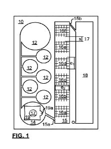
[0036] FIGs. 1-6 show a variety of patterned films for forming microfluidic
chips. In
these variants, common reference numerals identify equivalent or substantially
equivalent
features, and their descriptions will not generally be repeated herein. Each
variant has one
CA 03169871 2022-08-02
WO 2021/156844
PCT/IB2021/051007
or more independent features that are intended to be transposable on any of
the other
variants to produce further embodiments of the invention.
[0037] As is conventional, a stack of patterned films with suitable through-
holes (vias)
interconnecting channels of respective patterned surfaces can be assembled to
produce a
chip having a variety of functions. A simplest stack is a single patterned
film with a cover.
The layers may advantageously be composed of biocompatible plastics, and at
least
alternating layers may advantageously be thermoplastic elastomers as these can
be
patterned at a low cost, and form sealing bonds with many other materials, as
taught in US
10,369,566. In particular, Applicant has found that inclusion of two or more
layers of hard
thermoplastic layers, such as Zeonor, and at least one TPE layer between the
each pair of
Zeonor layers, such as an oil-free MedipreneTM (US 9,238,346), is particularly
efficient as:
low cost patterning and bonding can be provided with excellent seals; a
stiffness of Zeonor
layers assists in registration and alignment of the chip or stack; and Zeonor
can offer
excellent transparency, while Mediprene can provide an opaque back drop for
contrast.
[0038] The chip typically has a plurality of reservoirs (usually vented, or
controllably
vented see US 10,702,868, FIG. 11) for holding reagents, and other fluids, and
some
mixing chambers, the chambers and reservoirs being interconnected by a network
of
channels. Some operating mechanisms for controlling fluid movements within the
chip are
reliant on embedded features such as conductive electrodes and leads therefor,
valves,
and surface treatments and/or patterning of surfaces (capillary force
engineering) or walls
of microfluidic channels or chambers. Others require a layout of the chip to
have a
consistent positioning of ports and channels with respect to chambers, so that
a centrifugal
field gradient can control movement. In general, closed fluid dynamics require
venting and
a motive force. Furthermore, by incorporation of other elements into the chip,
either
between the layers of the chip, or around the chip, or by placing the chip in
proximity to
other elements, select regions of the chip, or content therein, may be acted
upon (heated,
cooled, irradiated, sonicated, activated, probed or sensed). Keeping such
elements outside
of the chip can permit cost-effective single-use chips, but for some
applications local
metallization, magnetization, treatment, or alteration, is needed to embed
essentially
passive elements within the chip to act upon the region or the content.
[0039] FIG. 1 is a schematic top plan view of a patterned film 10 showing
all of the relief
structure necessary to define a stand-alone microfluidic chip, in conjunction
with a covering
part or layer which is removed for illustration purposes. While, in principle,
most microfluidic
devices can function without an enclosure, the risks of contamination,
evaporation issues,
11
CA 03169871 2022-08-02
WO 2021/156844
PCT/IB2021/051007
and reliability require covers for each patterned layer. Film 10 requires a
cover (not shown)
so blisters 12, and a pump region 14 can be pressed.
[0040] In accordance with the present invention, one of the cover and film
10, is
transparent for inspection for read-out purposes, at least where required.
Transparent for
inspection may be transparent in one or more wavelength bands of an infrared,
optical, or
ultraviolet spectrum. While the whole cover or film 10 may be transparent,
only an area
covering interface pinning reaction vessels 16 need be transparent. Preferably
only one of
the substrate and cover is transparent to avoid issues with multiple images at
different
depths of view. So, the film 10 can be transparent and the cover can be
reflective, or
opaque, with a color and texture provided for good imaging contrast.
[0041] Film 10 as illustrated is adapted for mechanical actuation via an
array of blister
chambers 12, and a finger pump 14 on a supply side of the chip 10 (left as
shown). The
blister chambers may be small enough to be microfluidic chambers, though
typically they
have footprint of 0.1-20 cm2, and volumes 0f45 cm3 or more, which is large
fora microfluidic
chamber, but is nonetheless a reservoir for present purposes. A useful blister
for
microfluidic chips is disclosed in Applicant's US 10046893, which is
incorporated herein by
reference. Relief patterning of vessels may procedurally or structurally
resemble that of a
gating region disclosed in US 10046893.
[0042] Film 10 has a large flow-through chamber 15 provided in
communication with
the pump 14 via a microfluidic channel. Specifically, inlet 15a of the chamber
15 is part of
a microfluidic channel communicating with the pump 14 on the supply side of
the chip, and
outlet 15b communicates with a chip waste port 18. Herein a microfluidic
channel is
understood to have a channel direction (at least locally), and a nominal
channel width and
depth perpendicular to the channel direction that are each less than 900 pm,
more
preferably from 1-300 pm. In the embodiment of FIG. 1, the nominal channel
widths and
depths may be from 50-500 pm.
[0043] At least one wall of the chamber 15 (floor as shown), defines 6
regions with
respective micro- or nano-structured relief patterns respectively defining
vessels 16. The
relief structures, which may be recesses in, or protrusions from, the floor
(or other wall)
may have any form or arrangement, pillars, walls, fences, or lattices of any
cross-sectional
shapes or variances. The regions are preferably composed of a material that is
naturally
hydrophilic, or is coated or activated to induce capillary effect, at least
with respect to liquids
used for functionalization of the vessels 16. There are no transverse walls or
partitions
between the vessels 16 within the chamber 15 apart from micro- or nano-
structuration
12
CA 03169871 2022-08-02
WO 2021/156844
PCTIIB2021/051007
which does not impede, but rather encourages, flow through the chamber 15. As
such, the
regions are separated by segments of the floor that are relatively smooth,
either lacking in
any patterned relief, or having much lower surface area for footprint area
(e.g., having a
relief pattern depth markedly less than that of the floor within one of the
regions, or having
fewer or otherwise lower surface area features).
[0044] Herein, a footprint area refers to a 2D area enclosed by a perimeter
of the
region. In FIG. 1, each region has a same perimeter, and the footprint area is
its length
(extent ei) times its width (extent e2). If the chip is 10 cm long and 6.8 cm
wide, e2 is about
1.2 cm, ei is about 1 cm, and the vessel footprints are 1.2 cm2. However, the
surface area
of the vessel is at least 1.44 cm2, more preferably at least 1.92 cm2, and can
be 1 to 2
orders of magnitude higher. For example, a regular array of pillars with
uniform cross-
section (square, regular polygonal, circular, etc.) of 40 pm perimeter, in a
2D packing (e.g.
square, hexagonal, regular basis) with 50% duty ratio, and an aspect ratio of
8:1, has a
surface area of 33x footprint. The region can be a regular tiling or an
irregular mosaic. The
pillars may be tapered or have varying cross-sections, or can be replaced by
wall segments
or branched structures. Every shape in positive relief has an analogous,
equally useful,
hole in negative relief.
[0045] The regions are shown arrayed in series, labelled a-f. While this
may be
convenient, in other embodiments the vessels 16 may be arranged in a
rectangular array,
a staggered or off-set array, or other arrangement that assists in readout.
Preferably, a
spacing (s) between the vessels 16 is regular. A spacing of at least 5% of the
mean
dimensions of the regions, and at least 0.1 mm may allow visualization. Better
visual
separation of the vessels may be provided with larger spacing, such as 0.2 mm
and 15%,
or 0.3 mm and 20%. As shown in FIG. 1, the separation is about 0.4 mm, which
is about
40% of ei (which is the direction of the separation).
[0046] While the shapes, sizes, orientations and positions of the vessels
16 may be
regular, within each region, there may be a variation in density of
micropillars, microholes,
or other microstructures. Specifically, it has been noticed that with uniform
density of
micropillars, in use, a peripheral area of such regions tend to be more
strongly colored than
an interior region, particularly if a probe density is weak. To improve
consistency and ease
of qualitative/quantitative assessment, within each region, various density
gradients of
features may be preferred to provide different wicking forces across each
region.
Furthermore, wicking forces can be directed by selective orientations of
groups of features,
to encourage flow across the chamber 15.
13
CA 03169871 2022-08-02
WO 2021/156844
PCT/IB2021/051007
[0047] Furthermore, while the pillars may extend a full etch depth of the
chamber 15,
in some embodiments they advantageously only extend above or below a nominal
floor of
the chamber, by a fraction of the etch depth. For example, the micropillars,
may extend
between 20% to 100% of an etch depth. If microholes are used, they may extend
10%-
200% of an etch depth of the floor from which they extend.
[0048] The chamber 15 preferably covers at least about 10% of the footprint
of the chip,
and preferably extends at least 60% of a length of the chip. As shown in FIG.
1 about 15%
of the footprint of the chip is occupied by the chamber 15, and the chamber 15
extends
about 90% of the chip's length. The six separated regions of micro- or nano-
structured
topography (i.e. the vessels) are arrayed in chamber 15, which is otherwise
undivided in
that no partitions or walls separate the vessels 16. The chamber 15 provides
spacing 17
between the vessels 16 that facilitate read-out of colored or marked liquid
retained therein.
The chamber 15 may have an elongated shape with a large number of vessels 16
in a
regular array. Each region is sized and separated to ensure inspection of the
region
independently of others, and are preferably maximally distributed within the
chamber 12.
[0049] Any manner of marking of the film 10, or cover, may be used to
facilitate
identification of vessels 16 by their binding targets, for example. In
particular, a cover may
have a set of demarcating lines imprinted thereon for delineating respective
vessels, to
assist in viewing. If the cover is thin and transparent for inspection,
reliable demarcation is
possible with suitable alignment of the cover, over a range of viewing angles.
[0050] The embodiment of FIG. 1 can be sold as a patterned film 10, and the
vessels
thereof may be functionalized by a first buyer. The functionalized patterned
film may be
protected by applying the cover, temporarily or permanently, to form a chip.
The covered
film may be loaded so that blisters 12 retain various liquids (before or after
application of
the cover) by the first buyer, or a buyer of the functionalized patterned
film. In general the
liquids may be classed as one set of liquids necessary for sample preparation,
and another
set of liquids implicated in a marking process. In the illustrated embodiment,
there may be
no sample preparation on the chip. At this juncture, the chip may be ready for
deployment.
If the liquids are stable and the blisters are hermetically sealed, this chip
may be stored for
extended periods before use.
[0051] In use, a user may inject a sample into pump region 14, by peeling a
resealable
covering 19 (from a gripping ear 19a), and then reseal it. Instead the
covering may be
designed to reseal from a puncture and the sample may be injected by a
syringe. The
resealable covering 19 preferably overlies a cover that defines a finger pump-
area,
14
CA 03169871 2022-08-02
WO 2021/156844
PCT/IB2021/051007
although the covering is not in view. Preferably, the pump region 14 is filled
above a
minimum fill line, representing a minimum fill volume required for reliable
testing, without
overfilling. The user then presses on the pump region 14, and liquid,
following the path of
least resistance, passes through the ingress 15a, into chamber 15. By
releasing the pump
region 14 air may be aspirated into the pump region 14 to equilibrate pressure
within the
pump region 14 to minimize backflow into pump region 14. Alternatively, by
bursting one
of the blisters 12, and releasing pressure on the pump region 14, liquid from
the blister can
load into the pump region 14. Thus air aspiration may occur only at the
blister, on the
microfluidic channel by a user controlled valve, or at the pump region 14, and
as a result
each delivery of liquid may be separated by an air plug, or may be
incorporated into a train.
[0052] A volume of the blisters 12 may be an integer number of a volume
within
chamber 15, whereby content of each blister (or an equal division thereof)
may, in turn, fill
the chamber 15 in accordance with a prescribed protocol, although this is not
necessary,
and one vessels may be exposed to one agent while another is exposed to
another.
[0053] Herein a number of variants of the film 10 are provided. While these
may share
little in form, they all have in common a flow-through chamber 15 with four or
more
vessels 16 defined by higher surface area relief patterns, and some kind of
microfluidic
network that couples two or more reservoirs to an ingress 15a. The various
embodiments
may further have reservoirs for processing liquids, which may be used
regardless of the
format of the chip.
[0054] FIG. 2 is a schematic illustration of a patterned film 10 suitable
for pneumatic
(off-chip) pumping, or hydraulic, syringe-based injection. A chip formed with
film 10 might
also be driven suitably with a variety of electroosmotic, EWOD on-chip pumps
such as
Applicant's co-pending US Patent Publication 2016/051935 entitled "Peristaltic
pump
microfluidic separator", or mechanical pumps, but is not suitable for
centrifugal operations,
given the layout. This film 10 may also be designed as for use as a stand-
alone chip
(requiring no other patterned film to be joined in a sandwich structure), if
so a first port 22
is provided for receiving a sample, and possibly a chasing liquid (an inert
dense liquid
chosen for non-reaction with the sample). The first port 22 may be a standard
(e.g., Luer
lock) or non-standard coupling, and may be defined by a through-hole in the
film 10, or a
through-hole in a cover aligned with the film 10. The port 22 may be a simple
hole with a
smooth cylindrical surface of known resilience, for meeting a suitable tube,
or may have
tube attachment rims for locking or attaching to a tube. If the chip or cover
has rims or
protrusions, it may be manufactured by injection molding. Alternatively any or
all of the
CA 03169871 2022-08-02
WO 2021/156844
PCT/IB2021/051007
ports 22,12,23,18 may be for coupling to another microfluidic network on an
adjacent film
having corresponding vias in alignment.
[0055] The sample liquid will first enter a long sorting channel 25 that
may function by
inertial confinement, or may have an offset array of microfeatures for
deterministic lateral
displacement, that separate particles in the sample. As microfeatures are
required for the
vessels, a finesse of the patterning of the substrate is already required to
permit such
features. The outside streams are withdrawn into ports 23 with suitable
pressure at those
ports, and an inside stream is ejected into a mixing chamber 26. Once a
retained fraction
of the sample (the inside stream) enters the mixing chamber 26, it will begin
to fill the mixing
chamber. Once it fills sufficiently to meet a wall opposite the entry from the
sorting
channel 25, the retained fraction forms a liquid plug that separates two ports
24 that are
directly coupled to the mixing chamber 26. The mixing chamber 26 may overlie a
heater
or cooler to apply a desired temperature in accordance with a desired protocol
for the chip,
and one or more liquids may be injected into the mixing chamber 26 via these
two ports 24.
Once the retained fraction is treated in the mixing chamber 26, a pressure in
one or more
of the ports 22,23,24 is made higher than that of waste port 18 (ports 12 and
the rest of the
ports 22,23,24 being blocked or of higher pressure than waste port 18). As a
result, the
treated liquid is imbibed into flow-through chamber 15, via a plurality of
openings 15a. A
liquid front of the treated liquid passes each vessel 16 in sequence as an air
plug is
withdrawn from port 18 via outlet 15b. By controlling a rate of evacuation
(via the difference
between the low pressure of port 18 and the higher pressure at the one or more
of ports
22,23,24) a dwell time of the sample within each vessel 16 can be controlled.
The higher
pressure may be provided by a chasing liquid, or even a gas such as a sterile
gas injected
under positive pressure, or by applying a negative (relative to ambient)
pressure at the
waste port 18. If the chasing fluid has a density higher than the treated
liquid, it may replace
the treated liquid within the vessels 16. Alternatively, the bulk of the
sample may be
withdrawn from the chamber 15, for example with the pressure difference,
leaving only filled
vessels of the treated liquid, in an otherwise gaseous chamber. Subsequent
heating,
negative pressurization, and/or gas flow through the chamber 15 can be used to
evaporate
or reduce the treated liquid to increase concentration, and encourage capture
of any
analytes for which the vessel is functionalized. Subsequent wash stages (wash
introduced
via the one or more of ports 22,23,24, another of these ports, and/or one or
more of
ports 12) can be performed to remove any residue within the vessels 16.
[0056] Subsequently a marking process is performed, which involves
injection of fluids
through ports 12, passage of a liquid fluid front across the vessels 16 in
sequence, and exit
16
CA 03169871 2022-08-02
WO 2021/156844
PCT/IB2021/051007
through waste port 18. There may be several steps in this process, and a
particularly
invented process is described hereinbelow for use on COC substrates. At the
end of the
marking process, the vessels 16 can be read-out, preferably with the naked
eye, and/or
from a photographic record.
[0057] FIG. 3 is a schematic illustration of a film 10 patterned to define
a centrifugal
microfluidic chip designed for mounting to a centrifuge on an axis as shown.
The chip's
surface is partitioned into 3 areas for marking, sample prep, and readout. The
chip (by
virtue of a through-hole in the film 10, or a through-hole in a cover)
comprises an array of
7 ports/vents: 5 controlling respective chambers 12 for performing a marking
process (on
the marking area), and two controlling respective chambers 14,20 (on the
sample prep
area). The chip may be designed for mounting to a microfluidic chip
controller, according
to Applicant's US 10702868 "Centrifugal microfluidic chip control", or to a 7-
path rotary
coupling/pneumatic slip ring. In particular, this chip, with liquids preloaded
in each of these
7 chambers, is designed for complete dispensation with a suitable air plug and
a
controllable valve mounted to the centrifuge. This particular control strategy
is particularly
suited to simple processes and chips with inexpensive centrifuges and chip
controllers, and
can be automated for performance during a continuous centrifugation process
without user
intervention. For such applications, it is particularly useful to provide the
chips preloaded
with all liquids in an enclosed device, except for the test sample, which gets
introduced via
resealable covering 19, prior to mounting to a portable centrifuge for
automated processing.
[0058] The sample prep area includes a chamber 20, and sample chamber 14.
The
chamber 20 and sample chamber 14 jointly feed a mixing chamber 26 in a
particular
manner that allows for highly efficient droplet mixing according to the
teachings of
Applicant's L. Clime, T. Veres "Centrifugal microfluidic mixing apparatus and
method"
CA2864641. Specifically a constriction at the entrances to the mixing chamber
26 from
both chambers 14,20 results in fluid being dispensed as a discrete sequence of
droplets.
The droplets fall under the centrifugal force, and slide down an inclined
surface. The tiny
volumes of these droplets encounter one another and diffuse quickly as they
have very
high surface area to volume ratios, and fall into a belly of the mixing
chamber 26 in a well
mixed state. Once the mixture fills the belly, and primes a siphon valve, the
mixture is
ejected all at once into the flow-through chamber 15, filling the flow-through
chamber. A fill
line is shown for this chamber. As long as a total volume of liquid in
chambers 14 and 20
are more than enough to fill the belly once, and not enough to fill it a
second time, there will
only be a single dispensation of a metered volume.
17
CA 03169871 2022-08-02
WO 2021/156844
PCT/IB2021/051007
[0059] As such,
rote operation of the chip defined by film 10 will initially involve opening
the two right ports, to allow release of liquid in both chambers 20 and 14,
while the loaded
chip is under centrifugation. The two right ports may be operated by a common
valve that
is preferably located on a chip holder or chip controller such that the valves
are never
contaminated by any fluid and can be used on many chips in sequence. Release
to ambient
allows the fluid to drop into the constriction, and drip into the mixing
chamber 26, where the
droplets are mixed and accumulate in the belly until full. The fluid then
empties into
chamber 15, where it wets the vessels 16 in sequence, and preferably fills the
volume of
chamber 15. Subsequently one chamber 12 at a time is released to ambient to
allow
complete dispensation of the fluid contained therein, which flows directly
into the
chamber 15, displacing the sample and forcing the sample to exit via a drip
end that
conforms with a device taught in Applicant's co-pending PCT/IB/2019/059715
entitled
"World-to-chip automated interface for centrifugal microfluidic platforms".
Each
dispensation from chamber 12 may fill the whole chamber 15, or may produce a
train of
fluid segments that each treat each vessel 16 in sequence.
[0060] FIG. 4 is
a variant of the film 10 of FIG. 3, adapted for a different control strategy.
Instead of pressure control at valves, dispensation is controlled by
respective
hydrodynamic restrictions on the sample prep area, and angular tilting of the
chip relative
to the centrifugal field defined by an axis that is above the chip as
illustrated. The angular
tilting is provided by swivel mounting of the chip on an axis (shown at top
right of film 10),
for example in accordance with the teachings of Applicant's co-pending US
2017/0173589
entitled "Swivel mount for centrifugal microfluidic chip". An equally
automated process for
going from loaded chips to answer can be provided with this variant, by
providing a control
over the swivel mounting according to a prescribed process. Specifically, for
the designed
film 10, the process will involve a zero angle for an initial period during
which the sample
and content of chamber 20 are mixed, the belly is filled, and the mixture is
delivered in to
chamber 15, and then a sequence of tilts for delivering contents of chambers
12a-e. As
shown the sequence could be in alphabetical order, or d,e,a,b,c, depending on
whether the
chip is first tilted right or left. Alternatively any sequence with d before
e, a before b, and b
before c can be performed.
[0061] While the
foregoing films 10 have all provided relatively small surface areas for
readout, depending on a number of analytes and a desired sensitivity, it may
be preferable
for a larger surface area to be devoted to readout. A multistage protocol for
sample
preparation can be provided on a parallel layer of a centrifugal microfluidic
chip without
reducing a footprint of the readout area. As such the chamber 15 may occupy
more than
18
CA 03169871 2022-08-02
WO 2021/156844
PCT/IB2021/051007
half of the chip, as shown in FIG. 5. Specifically FIG. 5 is a chip designed
for operation by
an articulated blade, as in the example of FIG. 4, using only 5 chambers.
Sample prep is
provided by a separate chip layer, and may be provided by pneumatic control,
or centrifugal
microfluidics. If provided by articulated (swivel mount) centrifugal
actuation, efforts to avoid
dispensing in the marking area during sample prep processing. With few
chambers, it is
relatively easy to assign dispensing tilt angles to respective processes. Once
the sample
prep process is completed, the liquid to be tested is supplied through a via
to port 17* under
centrifugation at zero tilt angle. For easier appreciation of the angle at
which dispensation
occurs, each of the chambers 12 has an identified fill level. It will be noted
that the fill level
aligns with an edge of an open port 17 such that each chamber may be designed
to be
overfilled, and during centrifugation, excess will leak out at the top
surface. A top surface
may also be patterned to avoid cross contamination if that is a risk. It will
be noted that a
small clockwise rotation of the swivel mount about the axis on top right will
dispense
chamber 12a, a larger clockwise rotation, will dispense chamber 12b, and
progressively
larger tilt angles in the counterclockwise direction dispense chambers
12c,d,e.
[0062] FIG. 6 is a schematic illustration of a chip consisting of a
patterned film 10
covered by a cover 28 that is shown transparent to offer a ghost view of the
patterned
film 10. A via 15a is the only feature shown on the cover 28, although the
cover could be
patterned on a near side to produce any microfluidic structure required for
sample
preparation and/or for marking. The chamber 15 occupies a vast majority of the
film 10,
sharing this space only with waste reservoir 18. In other embodiments, the
chip may have
an exit port similar to the embodiments of FIGs. 2-5, to avoid a need for the
waste
reservoir 18, and thus the chamber 15 can substantially occupy the whole
chip's surface
area on one layer.
[0063] While the cover 28 is shown transparent, to provide the ghost view,
and bearing
a via serving as entry 15a into the chamber 15, it is logically preferable for
an outside film
of the chip to be transparent for inspection, such as reasonably transparent
across a visible
spectrum or at least for colors of the marking. Furthermore it is preferable
for the cover, as
shown, to be substantially opaque at those wavelengths, to provide contrast
for the color(s).
It will be appreciated that a stack of several layers may be used to produce
chips according
to the present invention.
[0064] While film 10 of FIG. 6 is not a complete embodiment of the instant
invention, it
will be appreciated that any chip including the film 10 that has two or more
fluidic paths
leading from respective reservoirs or supplies to the via 15a, and preferably
at least three,
or at least four such fluidic paths, will present a complete embodiment.
19
CA 03169871 2022-08-02
WO 2021/156844
PCT/IB2021/051007
[0065] FIG. 7 is a schematic illustration of an activation scheme for a
patterned film
(substrate) used for a particular marking process defining a colorimetric
assay, found to
work well on patterned films composed of COC. The process begins with
preparation of
the film for, and immobilization of amino-modified oligonucleotide probes. The
surface
preparation comprises the following steps:
= Expose substrate (vessel regions) to oxygen plasma to release hydroxide
groups
(first stage of FIG. 7)
= Expose freshly oxidized substrates to a 0.5 M solution of cyanogen
bromide (CNBr)
in acetonitrile at room temperature e.g. for a duration of 5 to 10 min
= Rinse substrate with cold acetonitrile and dry with a stream of nitrogen
gas (second
stage of FIG. 7)
= Apply respective target-bearing solutions of amino-modified
oligonucleotide probes
[e.g., 100 pM in deionized water] to pillar arrays: the solutions propagate
across the
array by capillary forces to fill the vessels
= Allow DNA solution to dry out, to form spotted vessels on the film
= Incubate spotted film at 95 C for 10 min to complete binding
= Rinse substrates 5 times with PBST (0.01 M phosphate-buffered saline, pH
7.2,
containing 0.05% v/v Tween 20) to wash excess oligonucleotide molecules off
the
surface, followed by drying with a stream of nitrogen gas (third stage of FIG.
7)
[0066] At this stage the vessels are individually spotted and can be stored
for several
months before use. The storage can be before or after loading the chip, or
even forming
the chip by bonding at least a cover to the chip. The chip may advantageously
be bonded
to a COC substrate if the cover 28 is composed of a thermoplastic elastomer,
such as
taught in Applicant's US 9,238,346 and US 10,369,566.
[0067] Loading of the chip, according to this colorimetric marking process,
involves
loading into respective chambers 12:
1) Transfer 50 pL of DIG-labelled multiplex PCR products in a 1.5 mL
microcentrifuge tube (use lid-locks' or screw-cap tubes to prevent the caps
from
popping while heating). Denature PCR products in a heating block at 100 C for
10
min, followed by snap-chilling on ice water for 5 min. Pulse spin tubes in a
CA 03169871 2022-08-02
WO 2021/156844
PCT/IB2021/051007
centrifuge to bring down condensation before opening the tubes during the next
step.
2) Add 150 pL of ice-cold hybridization solution (HS) containing 50%
formamide to the 50 pL of denatured, labelled PCR products.
3) Saturate the pillar arrays with the HS + 50% formamide + PCR product and
incubate for 20 min at 45 C. Wash the substrates 5 times with PBST.
4) Add a freshly prepared solution of anti-DIG-POD in 0.5% PBST-B (1:2,000
v/v) to the substrate. Incubate for 10 min at room temperature. Wash the
substrate 5
times with PBST.
5) Add 3,3',5,5'-tetramethylbenzidine (TMB) membrane peroxidase substrate.
Protect from light. Let the color develop for 10 min or so. Take photographs
of the
samples using a camera or documentation system on a UV transilluminator.
[0068] An example of a colorimetric assay performed on elongated
micropillar arrays
is shown in FIGs. 8,9. FIG. 8 is a photograph of a ZeonorTM COC substrate
containing
vessels produced by hot embossing along with scanning electron micrographs
showing a
close-up view of the microstructured area. The pillars are arranged in a
lattice. FIG. 9 is a
photograph showing good contrast and accuracy of the blue-colored spots and
high
specificity between spotted (odd-numbered) and non-spotted (even-numbered)
regions.
[0069] From a design point of view, micropillar arrays can generally be
reduced to a
particular type of unit cell, which repeats itself multiple times in both x-
and y-directions.
The characteristic parameters for the array are also found in the unit cell.
This includes the
dimensions of each pillar as well as its position with respect to neighboring
pillars. FIG. 10
shows an example of a pillar array unit with hexagonal packing. Here, each
pillar (which
has a circular footprint) is characterized by the diameter D and the depth d.
Their
configuration within the unit cell is defined by the pitch P, the inter-pillar
distance G, and
the tilt angle e (which is 60 in the case of a hexagonal packing). All
parameters determining
the unit cell can be varied either through the design (D, P, G, and e) or
through the
fabrication conditions (d). In this way, the layout of an array can be chosen
to achieve
desired conditions for reactivity and visualization. The colorimetric signal
therefore should
be tunable by the array design. Preliminary results depicted in FIG. 10A-H
confirm this
hypothesis. The structures included in this design indicate that an increase
in surface area
(through variation of P and D) leads to higher signal intensities.
21
CA 03169871 2022-08-02
WO 2021/156844
PCT/IB2021/051007
[0070] It is further possible to emphasize the vertical portions of the
pillars (e.g., by
introducing a pyramidal structure or a star-shaped cross-sectional profile, or
rounded cone).
Such a configuration would enable to potentially collect higher signals by
emphasizing the
vertical portions of each pillar.
[0071] Further, the wide area form (the geometrical confinement) of the
pillar structures
can be itself arranged into a shape, image, letter, number or other character
to aid
visualization and increase ease of user interaction. This may be particularly
useful for
testing by non-trained personnel, and home-based testing.
[0072] Micropillar arrays are also suitable for other, non-colorimetric
detection schemes
(e.g., based on fluorescence or surface plasmon resonance). Micropillar arrays
induce
roughness to the substrate which can lead to Mie scattering. This effect is
advantageous
for improving contrast and signal intensity on an otherwise transparent and
colorless
substrate that offers poor contrast.
[0073] Fabrication of pillar arrays in polymer materials is scalable at
relatively low cost.
They should therefore provide a suitable alternative to paper or other
reaction matrices
currently used for colorimetric assays.
[0074] Micropillar arrays also facilitate integration in a polymer-based,
microfluidic chip
which can be envisaged either as an insert or by embossing features
simultaneously with
the fluidic structures. A suitable chip design has been conceived and a first
series was
fabricated. Preliminary results indicate that discrimination of virus through
on-chip RNA
extraction and amplification is possible using a colorimetric detection assay.
[0075] FIG. 11A shows a photograph of a Zeonor substrate with micropillar
arrays of
different configuration produced by hot embossing. The configuration of each
array number
is depicted respectively in FIGs. 10A-H. FIG. 11B shows a photograph of a
micropillar
array substrate showing contrast provided by TMB development according to an
suboptimal protocol. Arrays were all modified with 0157 oligonucleotide
probes. The
substrate was exposed to DIG-labelled rtb0157 gene targets.
[0076] FIGs. 12A,B show a sample-to-answer chip for RNA-based virus
detection. The
chip has been used to perform sample lysis, multiplex PCR amplification and
colorimetric
identification. The array has been prepared for detecting 5 different target
species
simultaneously. In this example, a blue colored bar indicates the presence of
MNV. The
chip was operated with a centrifugal platform (Applicant's co-pending
U52017/0036208
22
CA 03169871 2022-08-02
WO 2021/156844
PCT/IB2021/051007
entitled Centrifugal Microfluidic Chip Control, the entire content of which is
incorporated
herein by reference).
[0077] Subsequent to the provisional filing, Applicant has produced further
examples
of the present invention. The use of polymer substrates other than Zeonor
(polystyrene
and polylactic acid) was demonstrated. Functionalizing different substrates
may call for
different processes.
[0078] The use of activation schemes other than oxygen plasma and cyanogen
bromide treatment has been demonstrated. Polylactic acid micropillars were
modified
using combined UV/ozone treatment followed by reaction with amino propyl
triethoxysilane
and glutaraldehyde. Applicant has successfully employed UV/ozone treatment on
polystyrene as an alternative to oxygen plasma treatment. Polystyrene
micropillars were
modified with oxygen plasma treatment, followed by reaction with amino propyl
triethoxysilane and glutaraldehyde. The micropillars were then spotted with
biotinylated
antibody (Goat pAB against Human Albumin) which was then revealed through HRP-
conjugated streptavidin and TMB conversion. FIGs. 13,14 respectively
illustrate the
contrast produced on the polylactic acid pillars, and polystyrene
micropillars, respectively.
Unfunctionalized vessels were interleaved between the functionalized vessels
to show
contrast provided by the target reporting.
[0079] Applicant has further demonstrated fluorescence-based detection as
opposed
to colorimetric detection. While colorimetric detection involves production of
a dye that can
typically multiply a strength of the signal offered by a reporting target,
fluorescent labelling
allows only the emissions of the target particles to report. The density and
arrangement of
target particles around micropillars provides a surprisingly strong observable
signal.
Fluorescence micrographs of a micropillar array (Zeonor) modified with a
biotinylated
antibody (Goat pAB against Human Albumin) at different concentrations and used
in a
fluorescence binding assay with Cy3-labelled streptavidin. The Zeonor surface
was
activated using oxygen plasma treatment, followed by reaction with amino
propyl
triethoxysilane and glutaraldehyde. Fluorescence intensity was found to
grow
exponentially as a function of probe concentration. FIGs. 15A,B,C,D,E form a
panel
showing fluorescent response of vessels exposed to 1, 5, 10, 50, and 100 pg/ml
concentrations of albumin.
[0080] In greater detail, the examples were produced as follows:
1) Microstructured Zeonor, polystyrene or polylactic acid substrates were
exposed to oxygen plasma for 2 min at a pressure of 50 mTorr, a power of
23
CA 03169871 2022-08-02
WO 2021/156844
PCT/IB2021/051007
100 W, and a gas flow of 20 sccm. Some polystyrene substrates were
alternativelyexposed to UV/ozone for 10 min.
2) Freshly oxidized substrates were incubated with a 2% aqueous solution of
amino propyl triethoxysilane for 1 h at RT. Samples were rinsed with DI
water and dried with a stream of nitrogen gas.
3) Samples were incubated with a 2% solution of glutaraldehyde in PBS for 2 h
at RT. Samples were rinsed with DI water and dried with a stream of nitrogen
gas.
4) Capture AB (200 pg/mL) was spotted on alternating interface pinning
reaction vessels using slotted pins (500 nL capacity). The samples were
stored in a Petri dish containing wet strips to maintain humidity. The Petri
dish was sealed to prevent evaporation and stored. Incubation times were
from 1h to 12 h.
5) Substrates were immersed in PBST + Casein blocking solution 1:1 (v/v) for 1
min and then rinsed with DI water and dried. No additional blocking step
seems to be necessary. If rinsing is done without blocking agent, traces of
protein from the spotted region to the outside areas are apparent on the
sample since the glutaraldehyde is still reactive at this stage.
6) Antigen solution is added for capture. Streptavidin-HRP as well as
Streptavidin-Cy3 have been used in conjunction with a biotin label for
colorimetric of fluorescence detection. Incubation for forming the
biotin/streptavidin complex lasted for 5 min (about 200 pL per sample).
7) Substrates are rinsed with PBST + Casein blocking solution 1:1 (v/v), DI
water and dried with a stream of nitrogen gas.
8) Samples with HPR-modified streptavidin were incubated with TMB
membrane peroxidase substrate for up to 1 h. Samples treated with Cy3-
labelled streptavidin were inspected using fluorescence microscopy.
[0081] Applicant has thus described a variety of embodiments of the present
invention,
and further demonstrated the ability to selectively report targets on
interface-pinning
reaction vessels. Other advantages that are inherent to the structure are
obvious to one
skilled in the art. The embodiments are described herein illustratively and
are not meant
to limit the scope of the invention as claimed. Variations of the foregoing
embodiments will
be evident to a person of ordinary skill and are intended by the inventor to
be encompassed
by the following claims.
24