Note: Descriptions are shown in the official language in which they were submitted.
WO 2021/202159
PCT/ITS2021/023598
REFERENCE SIGNAL CHANNEL ESTIMATION
CROSS REFERENCE TO PRIORITY APPLICATION
[00011 This application claims the benefit of priority of
U.S. Patent Application
No. 16/836,668, filed March 31, 2020 and titled "REFERENCE SIGNAL CHANNEL
ESTIMATION," the disclosure of which is hereby incorporated by reference
herein in its
entirety and for all purposes.
BACKGROUND
Technical Field
[0002] Embodiments of this disclosure relate to estimating
a channel in a
communications system using a reference signal.
Description of Related Technology
[0003] In a wireless communication system, it can be
desirable to have an accurate
estimation of a communication channel between a user equipment and a base
station. Certain
communication standards include reference signals that can be used to estimate
a
communication channel. Such a reference signal can be used to estimate an
uplink channel
from a user equipment to a base station. In certain applications, a downlink
channel from the
base station to the user equipment to the base station can be estimated based
on the uplink
channel. In real world wireless communication systems, a channel estimate can
be degraded
for a variety of reasons.
SUMMARY OF CERTAIN INVENTIVE ASPECTS
[0004] The innovations described in the claims each have
several aspects, no single
one of which is solely responsible for its desirable attributes. Without
limiting the scope of
the claims, some prominent features of this disclosure will now be briefly
described.
[0005] One aspect of this disclosure is a method of
reference signal channel
estimation. The method comprises receiving a reference signal for channel
estimation;
de-covering the reference signal in a frequency domain to generate a de-
covered reference
signal; after the de-covering, frequency domain processing the de-covered
reference signal to
CA 03170036 2022- 8- 30
WO 2021/202159
PCT/ITS2021/023598
cause distortion of a direct current offset in the de-covered reference signal
to be reduced; after
the frequency domain processing, time domain processing to cause a noise floor
associated
with the de-covered reference signal to be reduced; and generating a channel
estimate based
on the frequency domain processing and the time domain processing, wherein the
channel
estimate is associated with a communication channel between a first node and a
second node.
[0006] The frequency domain processing can comprise
generating an estimated
tone for a tone of the de-covered frequency domain reference signal based on
at least two other
tones of the de-covered frequency domain reference signal. The frequency
domain processing
can comprise replacing the tone with the estimated tone to cause distortion
associated with the
direct current offset to be reduced. The frequency domain processing can
comprise modifying
the tone based on the estimated tone to cause distortion associated with the
direct current offset
to be reduced.
[0007] The frequency domain processing can comprise pulse
shaping the de-
covered frequency domain reference signal to cause distortion associated with
the direct
current offset to be reduced.
[0008] The time domain processing can comprise estimating
noise power for a sub-
set of time domain taps corresponding to sub-carriers between channel impulse
responses, and
performing a per-tap scaling on at least a portion of the time domain taps
based on the
estimating. The per-tap scaling can involve minimum mean squared error
scaling. The per-
tap scaling can involve thresholding.
[0009] The method can further comprise pulse shaping the
reference signal prior to
the de-covering.
[0010] The method canfurther comprise rotating the
reference signal based on an
indicator of a frequency offset prior to the de-covering.
[0011] The time domain processing can comprise moving a
spur outside of time
domain windows for cyclic shifts of the reference signal. The method can
further comprise
pulse shaping the reference signal prior to the de-covering.
[0012] The reference signal can be an uplink Sounding
Reference Signal.
[0013] The first node can be a user equipment and the
second node can be a
network node. The first node can be a user equipment and the second node can
include a
remote radio unit. The first node can be a user equipment and the second node
can include a
2
CA 03170036 2022- 8- 30
WO 2021/202159
PCT/US2021/023598
base station integrated with an antenna front-end. The first node can include
a first remote
radio unit and the second node can include a second remote radio unit. The
first node can be
a first user equipment and the second node can be a second user equipment.
[0014] Another aspect of this disclosure is a system for
channel estimation. The
system comprises a frequency domain processing circuit, a time domain
processing circuit,
and a channel estimation circuit. The frequency domain processing circuit is
configured to
generate a de-covered frequency domain reference signal and to process the de-
covered
frequency domain reference signal so as to cause distortion associated with a
direct current
offset to be reduced. The time domain processing circuit has an input coupled
to an output of
the frequency domain processing circuit. The time domain processing circuit is
configured to
suppress time domain channel impulse response leakage. The channel estimation
circuit is
configured to generate a channel estimate based on an output of the time
domain processing
circuit, in which the channel estimate is associated with a wireless
communication channel
between a first node and a second node.
[0015] The frequency domain processing circuit can be
configured to generate an
estimated tone for a tone of the de-covered frequency domain reference signal
based on at least
two other tones of the de-covered frequency domain reference signal, and to
replace the tone
with the estimated tone to cause distortion associated with the direct current
offset to be
reduced.
[0016] The frequency domain processing circuit can be
configured to perform
pulse shaping on the de-covered frequency domain reference signal to cause
distortion
associated with the direct current offset to be reduced.
[0017] The time domain processing circuit can comprise: a
filter comprising a
plurality of taps; a noise power estimation circuit configured to estimate
noise power for a sub-
set of the taps of the filter corresponding to sub-carriers between channel
impulse responses;
and a filter tap scaling circuit configured to perform a per-tap scaling on at
least a portion of
the taps of the filter based on the estimated noise power.
[0018] The time domain processing circuit can be
configured to move a spur
outside of time domain windows for cyclic shifts of the reference signal.
3
CA 03170036 2022- 8- 30
WO 2021/202159
PCT/ITS2021/023598
[0019] The system can further comprise a second time
domain processing circuit
configured to pulse shape a reference signal, the second time domain
processing circuit having
an output coupled to an input of the frequency domain processing circuit.
[0020] The system can further comprise a second time
domain processing circuit
configured to rotate a reference signal based on an indicator of a frequency
domain offset to
thereby reduce the frequency domain offset, in which the second time domain
processing
circuit has an output coupled to an input of the frequency domain processing
circuit.
[0021] The system can further comprise a second frequency
domain processing
circuit configured to perform per-cyclic shift frequency domain processing,
wherein the second
frequency domain processing circuit is coupled between the time domain
processing circuit
and the channel estimation circuit.
[0022] The first node can be a user equipment and the
second node can be a
network node. The first node can be a user equipment and the second node can
include a
remote radio unit. The first node can be a user equipment and the second node
can include a
base station integrated with an antenna front-end.
[0023] The de-covered frequency domain reference signal
can be a de-covered
uplink Sounding Reference Signal.
[0024] Another aspect of this disclosure is a system for
channel estimation that
comprises: means for processing a de-covered frequency domain reference signal
so as to cause
distortion associated with a direct current offset to be reduced; means for
suppressing time
domain channel impulse response leakage, the means for suppressing having an
input coupled
to an output of the means for processing; and a channel estimation circuit
configured to
generate a channel estimate based on an output of the means for suppressing,
wherein the
channel estimate is associated with a wireless communication channel between a
first node and
a second node.
[0025] For purposes of summarizing the disclosure, certain
aspects, advantages and
novel features of the innovations have been described herein. It is to be
understood that not
necessarily all such advantages may be achieved in accordance with any
particular
embodiment. Thus, the innovations may be embodied or carried out in a manner
that achieves
or optimizes one advantage or group of advantages as taught herein without
necessarily
achieving other advantages as may be taught or suggested herein.
4
CA 03170036 2022- 8- 30
WO 2021/202159
PCT/ITS2021/023598
BRIEF DESCRIPTION OF THE DRAWINGS
[0026] Embodiments of this disclosure will now be
described, by way of
non-limiting example, with reference to the accompanying drawings.
[0027] Figure 1 is a schematic block diagram associated
with a reference signal
model.
[0028] Figure 2 is a schematic block diagram of hardware
of a user equipment of
Figure 1 that is arranged to generate a reference signal.
[0029] Figure 3 is a schematic block diagram of processing
circuitry arranged to
generate a channel estimate.
[0030] Figure 4A is a schematic block diagram of a first
part of processing circuitry
arranged to generate a channel estimate.
[0031] Figure 4B is a schematic block diagram of a second
part of processing
circuitry arranged to generate a channel estimate.
[0032] Figure 5 is a diagram that illustrates time domain
channel impulse response
separation for a reference signal with 8 cyclic shifts.
[0033] Figures 6A to 6E are block diagrams of parts of the
processing circuitry of
Figures 4A to 4B that can improve channel estimation according to certain
embodiments.
[0034] Figure 7A is a graph that illustrates a magnitude
of a de-covered Sounding
Reference Signal from two cyclic shifts with some distortion in direct current
and low
frequency tones.
[0035] Figure 7B is a graph illustrating distorted direct
current and low frequency
tones in a time domain.
[0036] Figure 8A is a graph illustrating a channel
frequency response in a
frequency domain.
[0037] Figure 8B is a graph illustrating power leaking in
a time domain associated
with the channel frequency response of Figure 8A.
[0038] Figure 9 is a graph that illustrates frequency
domain pulses with a timing
offset, a frequency offset, and no timing or frequency offset.
[0039] Figure 10 shows an example of interpolation for
reference signal channel
estimation.
CA 03170036 2022- 8- 30
WO 2021/202159
PCT/ITS2021/023598
[0040] Figure 11 shows an example of extrapolation for
reference signal channel
estimation.
[0041] Figure 12A shows a received frequency domain SRS
after an FFT is
performed with distorted low-frequency tones.
[0042] Figure 12B shows an SRS after applying quadratic
interpolation to 16 low
frequency tones.
[0043] Figure 12C shows an SRS after applying quadratic
extrapolation to 16 edge
tones on each side.
[0044] Figure 13A shows window functions for a rectangle
pulse and a raised
cosine pulse.
[0045] Figure 13B shows time domain tap powers relative to
a center tap for the
rectangle and raised cosine pulses respectively.
[0046] Figure 14A is a plot of an SRS with extrapolated
edge tones before
frequency domain pulse shaping.
[0047] Figure 14B is a plot of a frequency domain pulse-
shaping function.
[0048] Figure 14C is a plot of the SRS that includes
extrapolated edge tones after
frequency domain pulse shaping is applied.
[0049] Figure 15 is a diagram that illustrates time domain
channel impulse
responses for cyclic shifts after an inverse FFT has been performed.
[0050] Figure 16 is a flow diagram of an example method of
time domain channel
impulse response scaling based on a power delay profile.
[0051] Figure 17 is a schematic block diagram of a time
domain processing circuit
that can perform time domain channel impulse response scaling based on a power
delay profile.
[0052] Figure 18 is a schematic block diagram of
processing circuitry with time
domain pulse shaping.
[0053] Figure 19A is a graph of a rectangle pulse and a
raised cosine pulse in the
time domain.
[0054] Figure 19B is a graph of a sinc pulse and a raised
cosine pulse in the
frequency domain.
[0055] Figure 20 is a schematic block diagram of
processing circuitry with
frequency rotation to compensate for a frequency offset.
6
CA 03170036 2022- 8- 30
WO 2021/202159
PCT/ITS2021/023598
[0056] Figure 21 is a flow diagram of a method of
detecting cyclic shifts of a
reference signal in which spurs are moved into an unused time space.
[0057] Figure 22 illustrates the locations of the first
harmonic spurs for four cyclic
shifts.
[0058] Figure 23 is a diagram illustrating an example
multiple-input
multiple-output (MIMO) network environment in which channel estimation based
on a
reference signal can be performed.
DETAILED DESCRIPTION OF CERTAIN EMBODIMENTS
[0059] The following description of certain embodiments
presents various
descriptions of specific embodiments. However, the innovations described
herein can be
embodied in a multitude of different ways, for example, as defined and covered
by the claims.
In this description, reference is made to the drawings where like reference
numerals can
indicate identical or functionally similar elements. It will be understood
that elements
illustrated in the figures are not necessarily drawn to scale. Moreover, it
will be understood
that certain embodiments can include more elements than illustrated in a
drawing and/or a
subset of the elements illustrated in a drawing. Further, some embodiments can
incorporate
any suitable combination of features from two or more drawings. The headings
provided
herein are for convenience only and do not necessarily affect the scope or
meaning of the
claims.
[0060] In Long Term Evolution (LTE) and New Radio (NR)
systems, a Sounding
Reference Signal (SRS) can be transmitted from a user equipment (LIE) to a
Node-B for
estimating of an uplink channel. More generally, an SRS can be transmitted
from an antenna
of a first node to an antenna of a second node. For time-division duplex (TDD)
systems, the
SRS channel estimate (CE) can be used to estimate a downlink channel quality
based on
channel reciprocity. In multiple-input multiple-output (MIMO) systems based on
codebooks
and/or regularized zero-forcing (RZF) precoding, SRS CE can be used in
selecting a precoding
matrix. In such instances, it is desirable for the accuracy of SRS CE to be
high, especially in
RZF precoding applications. SRS CE can be used for calibration.
[0061] There are a variety of impairments in a real word
system that may degrade
the performance of SRS CE. Such impairments include without limitation one or
more of
7
CA 03170036 2022- 8- 30
WO 2021/202159
PCT/ITS2021/023598
frequency offset, timing offset, time domain channel impulse response (ClR)
leakage, or
distortion of relatively low frequency tones. In addition, the output SRS CE
of edge tones may
be inaccurate due to a discontinuity of the SRS in the frequency domain. In
this disclosure,
techniques to improve the performance of SRS CE are provided to make channel
estimates
more robust in the presence of one or more impairments.
Sounding Reference Signal
[0062]
In LTE and fifth generation (5G) NR, the construction of an SRS
typically
includes SRS sequence generation and the mapping to physical resources. SRS
can be
generated according to a relevant communication standard. SRS can be an uplink
SRS in any
suitable embodiment disclosed herein.
[0063]
In LTE and/or NR uplink transmissions, there can be dedicated orthogonal
frequency domain multiplexing (OFDM) symbols for SRS transmission to scheduled
UEs. In
each symbol, mSRS resource blocks for SRS can be shared by a group of UEs. All
sub-carriers
in the mSRS resource blocks for SRS can be divided into Kir orthogonal combs.
An
orthogonal comb can be a group of signals allocated at a given time that are
orthogonal in the
frequency domain. The number of resource elements Mzc, in each comb can be in
accordance
with Equation 1, where Mzc can represent a length of an SRS sequence.
1112;C: ¨ MSRSIV, /1(71:
(Eq. 1)
[0064]
In Equation 1, 4:8 is the number of sub-carriers in each resource block.
N
sc can be 12, for example. Within each comb, Mzc resource elements are shared
by up to
nC.5,tmw:
5RS
SRSs through different cyclic shifts. The transmission comb number Kir,
is specified
by the base station and can take the value of 2 or 4. The maximum number of
cyclic shifts
CSna
that can be supported by one comb can be a function of Kir as indicated by
Equation 2.
K ........................................................
cs,max rc
M
(Eq. 2)
SRS (12, A re = 4
8
CA 03170036 2022- 8- 30
WO 2021/202159
PCT/ITS2021/023598
[0065] For the UE to transmit an SRS over the mSRS
resource blocks, the UE
should generate an SRS sequence of length Mzc. The first step for the UE can
be to obtain a
base sequence ru,(n) of length Mzc, where n denotes the index of the allocated
tones. For a
given length Mzc, there can be 30 or 60 base sequences r,,,,,(n) that are
divided into groups,
where u E {0, 1, === , 29} is the group number. There can be one or two
sequences in one
group, and the base sequence index within a group can be v {0} or v {0, 1},
respectively.
[0066] For Mzc? 36, ru,,, (n) can be obtained from a Zado
if-Chu (ZC) sequence by
Equation 3.
LN n mod
¨ .)
=
C (Eq. 3)
[0067] In Equation 3, Nzc can be the largest prime number
such that Nzc < Mzc and
xq(m) is a ZC sequence of length Nzc that is obtained from Equations 4-1 to 4-
3.
(Eq. 4-1)
-3 .......................................................
q(m) = e NZC
¨
= [47 1/ 21 4-. v (-1)1217.1
(Eq. 4-2)
Nzc(u 1)/3 1
(Eq. 4-3)
=
[0068] The rity (n) for MZC < 36 can be generated
according to a 3rd Generation
Partnership Project (3GPP) standard.
[0069] Group and sequence hopping for SRS can be
configured. In group or
sequence hopping, a base sequence is selected by varying u and v for each SRS
symbol. In
many applications, group or sequence hopping can be disabled and the
calculation of u and v
is simplified as shown in Equations 5-1 and 5-2, respectively.
SR'S
itt ¨ nip mod 30
(Eq. 5-1)
v. 0
(Eq. 5-2)
9
CA 03170036 2022- 8- 30
WO 2021/202159
PCT/ITS2021/023598
SIRS
[0070]
In Equation 5-1, 11147 is given by the higher layer. In the following,
it is
assumed that group or sequence hopping is disabled and hence the base sequence
is denoted
as r(n) with the subscripts u and v being omitted.
[0071]
After the base sequence r(n) is obtained in each UE, the SRS sequence
r(n) can be generated by applying a cyclic shift in frequency domain according
to
Equation 6.
r(r)(n) ¨ ei2""i"tarz' f(n), for 0 < it < Al7c and 0 <c <
(Eq. 6)
[0072]
In Equation 6, c is the cyclic-shift index. Then, r(c)(n) are mapped to
an
allocated comb, converted to the time domain signal through an inverse Fast
Fourier Transform
(IFFT). The time domain signal can be transmitted over channels with channel
impulse
yz
response (CIR) h (t), 0 < c <
, to a specific antenna. An overall block diagram for the
SRS model is shown in Figure 1.
[0073]
Figure 1 is a schematic block diagram associated with a reference signal
model. In Figure 1, a plurality of UEs 10A, 10B, 10N wirelessly transmit SRSs
with different
cyclic shifts over respective channels 12A, 12B, 12N to a Node B 14. The
different cyclic
shifts can identify which device and/or antenna is wirelessly transmitting an
SRS. At a
summing point 13, the SRSs can be summed in the reference signal model. The
Node-B 14
can include a radio frequency (RF) downconverting block 16 and a sampling and
cyclic prefix
(CP) removal block 18. The RF downconvertine block 16 can downconvert a
received RF
signal. This downconversion can be to baseband, for example. The sampling and
CP removal
block 18 can sample the downconverted RF reference signal. The sampling and CP
removal
block 18 can remove a cyclic prefix. The Node-B 14 can generate time domain
receive
samples from SRSs received from the UEs 10A, 10B, 10N. The Node B 14 can be an
evolved
Node B (eNode B), a next generation Node B (gNode B) or replaced and/or
implemented
together with any suitable base station or network system.
[0074]
With the maximum number of cyclic shifts being 8, there can be 8 UEs and
8 channels in the reference signal model. Similarly, with the maximum number
of cyclic shifts
CA 03170036 2022- 8- 30
WO 2021/202159
PCT/ITS2021/023598
being 12, there can be 12 UEs and 12 channels in the reference signal model.
Any other
suitable number of maximum cyclic shifts and corresponding channels can be
implemented in
accordance with any suitable principles and advantages disclosed herein.
[0075] Although UEs are illustrated in Figure 1, the
principles and advantages
disclosed herein can be applied to channel estimation between any suitable
nodes arranged to
wirelessly communicate with each other. For example, SRS channel estimation
can be used
to estimate a channel between an UE and a network node, for example, as shown
in Figure 1.
The network node can be a base station integrated with an antenna front-end.
The network
node can include a remote radio unit (RRU) and a base band unit (BBU). As
another example,
SRS channel estimation can be used to estimate a channel between two network
nodes (e.g.,
between 2 nodes that include RRUs). As one more example, SRS channel
estimation can be
used to estimate a channel between two UEs. SRS channel estimation in
accordance with any
suitable principles and advantages disclosed herein can be applied to channel
estimation
between any suitable nodes arranged to wireles sly communicate information.
[0076] Although embodiments disclosed herein may be
described with reference
to the SRS for illustrative purposes, any suitable principles and advantages
disclosed herein
can be applied to channel estimation using any suitable reference signal
and/or any suitable
pilot signal.
[0077] Figure 2 is a schematic block diagram of hardware
of a UE of Figure 1 that
is arranged to generate a reference signal. Each UE 10A to lON of Figure 1 can
include the
hardware shown in Figure 2. The functionality described with reference to the
blocks of
Figure 2 can be implemented by any suitable physical hardware. The
functionality described
with reference to Figure 2 can be implemented in any suitable node arranged to
transmit an
SRS and/or other reference signal.
[0078] As illustrated in Figure 2, reference signal
generation circuitry can include
a base sequence generator 21, a phase ramping block 22, a resource element
mapping block 23,
an IFFT block 24, and a digital-to-analog conversion and RE modulation block
25. The base
sequence generator 21 can generate a base sequence. for example, as described
above. As one
example, the base sequence can be generated using Equation 3. The phase
ramping block 22
can apply a cyclic shift to the base sequence generated by the base sequence
generator 21. The
cyclic shift can be applied in the frequency domain. Each node (e.g., each UE
10A to lON in
11
CA 03170036 2022- 8- 30
WO 2021/202159
PCT/ITS2021/023598
Figure 1) can have a different cyclic shift applied by a respective phase
ramping block 22. The
resource element mapping block 23 can map the SRS sequence from the phase
ramping
block 22 to an allocated comb. Then the IFFT block 24 can convert the
frequency domain
cyclic shifted signal to the time domain by an inverse Fourier transform. A
cyclic prefix can
he added by the IFFT block 24. The digital-to-analog conversion and RF
modulation block 25
can convert the output of the IFFT block 24 to an analog signal and modulate
the analog signal
to a radio frequency. An RF signal provided by the digital-to-analog
conversion and RF
modulation block 25 can be wirelessly transmitted over a communication channel
to a Node 13
and/or other suitable hardware for channel estimation.
Reference Signal Channel Estimation
[0079] Processing circuitry can receive a reference
signal, such as an SRS, and
generate a channel estimate based on the received reference signal. The
channel estimate can
be for a relatively wide band SRS. Example signal processing will be described
with reference
to Figures 3 to 6E. The signal processing circuitry can perform improved
reference signal
channel estimation in accordance with any suitable principles and advantages
disclosed herein.
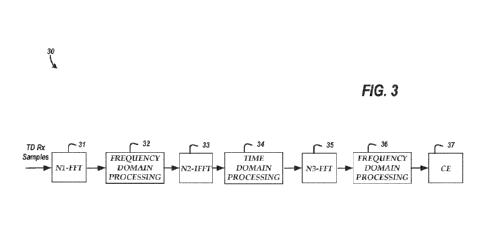
[0080] Figure 3 is a schematic block diagram of processing
circuitry 30 arranged
to generate a channel estimate. The processing circuitry 30 can receive time
domain reference
signal samples and generate a channel estimate based on the reference signal.
The time domain
samples can be received, for example, from a sampling and CP removal block 18
of Figure 1.
As illustrated in Figure 3, the processing circuitry 30 includes a Fast
Fourier Transform (FFT)
block 31, a first frequency domain processing circuit 32, an inverse Fast
Fourier Transform
(IFFT) block 33, a time domain processing circuit 34, a second FFT block 35, a
second
frequency domain processing circuit 36, and a channel estimation circuit 37.
[0081] The received reference signal can be an SRS. The
received SRS can be
converted into frequency domain by the FFT block 31. The frequency domain
processing
circuit 32 has an input coupled to an output of the FFT block 31. The first
frequency domain
processing circuit 32 can extract SRS symbols of a comb for de-covering. The
first frequency
domain processing circuit can de-cover the reference signal using a base
sequence. The de-
covered frequency domain reference signal can contain a sum of channel
frequency responses
with different phase ramping. Additional frequency domain processing can be
performed by
12
CA 03170036 2022- 8- 30
WO 2021/202159
PCT/ITS2021/023598
the first frequency domain processing circuit 32 after de-covering the
reference signal to
improve SRS channel estimate performance. The first frequency domain
processing circuit 32
can perform frequency domain processing to cause distortion of a direct
current offset and/or
a low frequency offset to be reduced. Examples of such processing will be
discussed below.
[0082] The IFFT block 33 can convert the de-covered
frequency domain signal
from the first frequency domain processing circuit 32 to the time domain. An
output signal
from the IFFT block 33 can be provided to the time domain processing circuit
34. The time
domain processing circuit 34 can perform time domain processing to improve SRS
channel
estimate performance. The time domain processing circuit 34 can perform time
domain
processing to cause a noise floor to be reduced. Examples of such processing
will be discussed
below. The time domain processing circuit 34 can separate channel impulse
responses.
Separating channel impulse responses can be performed in accordance with any
suitable
principles and advantages discussed with reference to Figure 6.
[0083] The second FFT block 35 can convert an output
signal from the time domain
processing circuit 34 to the frequency domain. The second frequency domain
processing
circuit 36 can perform per cyclic shift frequency domain processing. The
second frequency
domain processing circuit 36 can output a channel frequency response for each
cyclic shift.
[0084] The channel estimation circuit 37 can generate a
channel estimate based on
an output of the second frequency domain processing circuit 36. The channel
estimate is based
on the reference signal received by the processing circuitry 30. The channel
estimate is
associated with a wireless communication channel between a first node and a
second node. As
one example, the first node can be a UE 10A of Figure 1 and the second node
can be the
Node B 14 of Figure 1. Processing techniques disclosed herein can improve the
channel
estimate generated by the channel estimation circuit 37. This can be
advantageous in a variety
of applications, such as for selecting a precoding matrix in TDD MIMO systems.
[0085] More details regarding embodiments of the
processing circuitry 30 are
provided in Figures 4A and 4B and the corresponding description. Figure 4A is
a schematic
block diagram of a first part of processing circuitry 40 for generating a
channel estimate.
Figure 4B is a schematic block diagram of a second part of the processing
circuitry 40.
[0086] The processing circuitry 40 receives a reference
signal, such as an SRS. The
first FFT block 31 converts the received reference signal into the frequency
domain. A
13
CA 03170036 2022- 8- 30
WO 2021/202159
PCT/ITS2021/023598
reference signal extraction circuit 42 can extract all resource elements of
one comb for
de-covering. This can involve extracting SRS symbols of a current comb. The
summed SRSs
in the frequency domain can be represented by Equation 7. In Equation 7, He
(n) = (h(kT s)) is
the channel frequency response (CFR) of cyclic-shift c, and v(n) denotes the
additive white
Gaussian noise (AWGN).
= =
An) ¨ Ecs7 02/71,cfnsRs i'n
if(n) v(n), 0 < n < Mzc
(Eq. 7)
[0087] A base sequence generator 43 generates a base
sequence for de-covering.
The base sequence can be generated in accordance with any suitable principles
and advantages
disclosed herein. A mixer 44 or any other suitable circuit can be used to de-
cover the reference
signal using the base sequence from the base sequence generator 43.
[0088] After being de-covered by the base sequence r(n),
the de-covered frequency
domain signal can be represented by Equation 8. Equation 8 shows that the de-
covered
frequency domain signal contains a sum of channel frequency responses with
different linear
phase ramping.
,
nmlum,
An) r (it) z==:
h An) + t(n)õ 0 n < Aiztr.
(Eq. 8)
[0089] A frequency domain processing circuit 45 can
perform frequency domain
processing on the de-covered signal to improve reference signal channel
estimate performance.
[0090] Denote h(k) as a time-domain signal of length N and
define h(S)(k) as the
sequence by cyclic-shifting h(k) to the right by S, i.e., h(k) = h(MO D(k + S,
N)), for
0 < k < N. The de-covered signal yi(n) can be converted into time domain
through an IFFT by
the IFFT block 33. In the time domain, the signal becomes a combination of
multiple channel
impulse responses with different cyclic shifts, which can be represented by
Equation 9. In
Equation 9, Nirrr represents the IFFT size per comb.
14
CA 03170036 2022- 8- 30
WO 2021/202159
PCT/ITS2021/023598
47tir32-1 c
ten-
sift.) = IFFTOArt)) = h,nsfa S < N.
(Eq. 9)
[0091] After the IFFT, time domain processing can be
performed by the time
domain processing and channel impulse response separation block 48 of Figure
4B to improve
the SRS CE performance. Assuming that the maximum delay spread of any hc is
less than
;
nsfis , the time-domain channel for different cyclic shifts can be separated
relatively
easily by the time domain processing and channel impulse response separation
block 48. The
second FFT block 35 can include sub-FFT blocks 35A to 35N to transform
individual channel
impulse responses to the frequency domain. Per cyclic shift frequency domain
processing
circuits 50A to 50N can obtain the channel frequency responses for each cyclic
shift. A
channel estimation circuit, such as the channel estimation circuit 37 of
Figure 3, can generate
channel estimates based on the channel frequency responses for the cyclic
shifts.
[0092] Separating channel impulse responses will now be
discussed. Such
functionality can be performed, for example, by the time domain processing and
channel
impulse response separation block 48 of Figure 4B. To separate channel impulse
responses, a
window can be defined for each of the cyclic shifts. For a specific cyclic
shift, only taps falling
into the window for the specific cyclic shift are preserved and all other taps
can be set to zero.
Then, the non-zero taps are cyclic-shifted, and in the frequency domain, the
linear phase
ramping can be removed.
[0093] Figure 5 is a diagram that illustrates time domain
channel impulse response
separation for a reference signal with 8 cyclic shifts. The example shown in
Figure 5 illustrates
how to separate the channel impulse response for a specific shift (i.e., c =
7) from other cyclic
shifts. The top most portion of Figure 5 shows a time domain impulse response.
There are
time domain impulse responses for 8 different cyclic shifts shown in Figure 5.
There are
different windows defined for each of the cyclic shifts. Windowing can be
performed by
preserving a specific channel impulse response within a specific window (i.e.,
the channel
impulse response for cyclic shift c = 7 in Figure 5) and removing the other
channel impulse
responses. The impulse response for the specific channel can be shifted to
remove the cyclic
shift. This can remove linear phase ramping in the frequency domain.
CA 03170036 2022- 8- 30
WO 2021/202159
PCT/ITS2021/023598
[0094] Properties of ZC sequences in SRS will now be
discussed. If a ZC sequence
xq (m) defined in Equations 4-1 to 4-3 is de-covered by a shifted version of
itself, denoted as
xq (m ¨ s), s = 0, 1, 2 , 3, ... , the de-covered signal can be represented
by Equation 10.
nft (s2 s
In Equation 10, kv: can be a constant
phase.
zitsArt
X On) - s) c. e¨j Nz
= 11
(Eq. 10)
[0095] Equation 10 reveals that xq (m) = xq * (m ¨ s) is a
sequence of linear phase
z:u4
ramping, with the slope NZe being a function of s and q. If the frequency
hopping and
sequence hopping are disabled, then q becomes dependent on cell ID.
[0096] The IFFT of xq (m) = xq * (m ¨ s) represents an
impulse in time domain and
the delay of the impulse is related to s and q.
[0097] Frequency domain processing techniques can be
applied to improve
reference signal channel estimation. Such frequency domain processing can
reduce direct
current and/or other low frequency offsets. Alternatively or additionally,
frequency domain
processing circuits can compensate for any other suitable impairment to
accurate reference
signal channel estimation. The frequency domain processing circuit 32 of
Figure 3 and/or the
frequency domain processing circuit 45 of Figure 4A can implement frequency
domain
processing to improve reference signal channel estimation. Figures 6A, 6B, and
6C illustrate
example block diagrams of frequency domain processing circuits that can be
implemented by
the frequency domain processing circuit 32 and/or the frequency domain
processing circuit 45.
The frequency domain processing circuit 36 of Figure 3 and/or any of the
frequency domain
processing circuits 50A to 50N of Figure 4A can implement frequency domain
processing to
improve reference signal channel estimation. Figure 6D illustrates example
block diagram of
a frequency domain processing circuit that can be implemented by the frequency
domain
processing circuit 36 of Figure 3 and/or any of the frequency domain
processing circuits 50A
to 50N of Figure 4B.
16
CA 03170036 2022- 8- 30
WO 2021/202159
PCT/ITS2021/023598
[0098] Figure 6A is a block diagram of a frequency domain
processing circuit 62
according to an embodiment. The frequency domain processing circuit 62
includes a tone
estimation circuit 63 arranged to generate an estimated tone for a tone of a
de-covered
frequency domain reference signal based on at least two other tones of the de-
covered
frequency domain reference signal. The tone estimation circuit 63 is also
arranged to replace
the tone with the estimated tone to cause distortion associated with the
direct current offset to
be reduced. The tone estimation circuit 63 is can alternatively or
additionally modify the tone
based on the estimated tone to cause distortion associated with the direct
current offset to be
reduced. Tone estimation can involve interpolation. Tone estimation can
involve
extrapolation. Tone estimation can be based on poly-phase decomposition. Tone
estimation
can be based on least squares estimation. Tone estimation can be based on any
other suitable
technique. The frequency domain processing circuit 62 can perform any other
suitable
frequency domain processing for channel estimation, such as any other suitable
features
discussed with reference to the frequency domain processing circuit 32 of
Figure 3 and/or the
frequency domain processing circuit 45 of Figure 4A.
[0099] Figure 613 is a block diagram of a frequency domain
processing circuit 64
according to an embodiment. The frequency domain processing circuit 64
includes a channel
frequency response pulse shaping circuit 65 arranged to pulse shape a de-
covered frequency
domain reference signal. Pulse shaping can cause distortion associated with a
direct current
offset to be reduced. The pulse shaping can involve a raised-cosine pulse
and/or any other
suitable pulse. The frequency domain processing circuit 64 can perform any
other suitable
frequency domain processing for channel estimation, such as any other suitable
features
discussed with reference to the frequency domain processing circuit 32 of
Figure 3 and/or the
frequency domain processing circuit 45 of Figure 4A.
[0100] Figure 6C is a block diagram of a frequency domain
processing circuit 66
according to an embodiment. The frequency domain processing circuit 66
includes the tone
estimation circuit 63 and the channel frequency response pulse shaping circuit
65. Figure 6C
illustrates that tone estimation can be implemented together with channel
frequency response
pulse shaping. The frequency domain processing circuit 65 can perform any
other suitable
frequency domain processing for channel estimation, such as any other suitable
features
17
CA 03170036 2022- 8- 30
WO 2021/202159
PCT/ITS2021/023598
discussed with reference to the frequency domain processing circuit 32 of
Figure 3 and/or the
frequency domain processing circuit 45 of Figure 4A.
[0101] Figure 6D is a block diagram of a frequency domain
processing circuit 67
according to an embodiment. The frequency domain processing circuit 67
includes a scaling
circuit 68. The scaling circuit 68 can be implemented together with the
channel frequency
response pulse shaping circuit 65 of Figures 6B and/or 6C. The scaling circuit
68 can scale
the channel frequency response of edge tones to compensate for the impact of
frequency
domain pulse shaping. The frequency domain processing circuit 67 can perform
any other
frequency domain processing, such as any other suitable features discussed
with reference to
the frequency domain processing circuit 36 of Figure 3 and/or any of the
frequency domain
processing circuits 50A to 50N of Figure 4B.
[0102] Time domain processing techniques can be applied to
improve reference
signal channel estimation. In certain instances, time domain processing can be
implemented
together with one or more frequency domain processing techniques disclosed
herein to
improve reference signal channel estimation.
[0103] Figure 6E is a block diagram of a time domain
processing circuit 69
according to an embodiment. The time domain processing circuit 69 is arranged
to perform
time domain processing and channel impulse response separation. The time
domain processing
circuit 69 includes a channel impulse response scaling circuit 70. The channel
impulse
response scaling circuit 70 is arranged to scale a channel impulse response
based on a power
delay profile. The scaling can be applied per tap of a filter. The time domain
processing
circuit 69 can perform any other time domain processing, such as any other
suitable features
discussed with reference to the time domain processing circuit 34 of Figure 3
and/or the time
domain processing and channel impulse response separation block 48 of Figure
4B.
[0104] A time domain processing circuit can move a spur
outside of time domain
windows for cyclic shifts of the reference signal in certain embodiments. For
instance,
harmonic spurs can be moved to unused time domain space that does not impact
channel
estimation. Spurs can be moved to time domain indices below time domain
windows for the
cyclic shifts and/or to time domain indices between time domain windows for
cyclic shifts.
18
CA 03170036 2022- 8- 30
WO 2021/202159
PCT/ITS2021/023598
[0105] In certain applications, time domain pulse shaping
can be applied before a
reference signal is translated into the frequency domain. Time domain pulse
shaping can
reduce frequency offset and/or timing offset.
[0106] According to some applications, frequency rotation
can be applied before a
reference signal is translated into the frequency domain. This can reduce
frequency offset.
Impairments on Reference Signal Channel Estimation
[0107] In a real world communication system, there can be
a variety of impairments
that may affect the performance of reference signal channel estimation. Such
impairments can
include one or more of distortion of low frequency tones, time domain channel
impulse
response leakage, frequency offset, or timing offset. There can be a variety
of factors that can
result in inaccurate channel estimation. Identifying impairments that affect
performance of
reference signal channel estimation can be challenging. Impairments discussed
herein were
identified through analysis of SRS channel estimation data.
[0108] Distortion of low frequency tones will now be
discussed. For an RF front
end with a zero intermediate frequency (ZIF) transceiver, direct current (DC)
offset may be
present in a receive baseband signal due to local oscillator (LO) leakage. To
mitigate the DC
offset component, a notch filter can be applied to a demodulated signal before
generating
baseband samples for digital signal processing. However, the notch filter may
not work
perfectly and/or may distort the DC tone and one or more adjacent tones,
especially in TDD
systems where uplink symbols are not continuous in time.
[0109] If a DC tone and adjacent tones to the DC tone are
distorted, colored noise
can be introduced with locations at DC and low frequency tones in the
frequency domain. The
colored noise tones can elevate a noise floor in the time domain and introduce
inter-cyclic shift
interference in SRS CE.
[0110] Figure 7A is a graph that illustrates a magnitude
of a de-covered Sounding
Reference Signal from two cyclic shifts with some distortion in DC and low
frequency tones.
The distorted tones in Figure 7A are located at and near DC.
[0111] Figure 7B is a graph illustrating distorted DC and
low frequency tones in a
time domain. Sample power is plotted versus time index in Figure 7B. The
distorted tones
contribute to a hump in the time domain in the curve of Figure 7B. The
distorted tones are
19
CA 03170036 2022- 8- 30
WO 2021/202159
PCT/ITS2021/023598
located between channel impulse responses corresponding to different cyclic
shifts (i.e., c = 0
and c = 1 in Figure 7B). These distorted tones can raise the noise floor.
[0112] Time domain channel impulse response leakage will
now be discussed.
When a frequency domain channel frequency response is transformed into the
time domain
through an IFFT, the channel impulse response pulse may have a significant
sidelobe leakage
that goes into time domain windows for one or more other cyclic shifts.
[0113] Figure 8A is a graph illustrating a channel
frequency response in a
frequency domain. The channel frequency response for the cyclic shift c = 0 is
shown in the
frequency domain. In Figure 8A, the channel is relatively flat in the
frequency domain.
[0114] Figure 8B is a graph illustrating power leaking in
a time domain associated
with the channel frequency response of Figure 8A. After a 1024-point IFFT was
performed,
most of the energy is concentrated in a time domain window for the cyclic
shift c = 0, which
is between time domain indices 64 and 960 in Figure 8B. However, there can be
a
non-negligible portion of power leaked into other windows.
[0115] Sidelobe leakage can degrade the channel frequency
response of the cyclic
shift that the siclelobe leakage is associated with, which can be due to the
loss of signal power
in window truncating. Sidelobe leakage can degrade the channel frequency
response
performance of one or more other cyclic shifts by introducing inter-cyclic-
shift interference.
Therefore, ensuring that the channel impulse response of each cyclic shift is
concentrated in
its own time domain window can be significant.
[0116] Frequency offset will now be discussed. Even though
a UE can remove
most of the frequency offset between its local oscillator and a local
oscillator in a base station
through an initial acquisition and frequency tracking loop, there may still
exist a residual
frequency offset Af. Sometimes, the residual frequency offset can be as large
as several
hundred Hertz.
[0117] Unlike the demodulation of a Physical Uplink
Control Channel (PUCCH)
and Physical Uplink Shared Channel (PUSCH) where the frequency offset can be
estimated
and compensated for through a demodulation reference signal (DMRS), it can be
more
channeling to mitigate the frequency offset in SRS CE, especially when
considering that
different UEs may have different frequency offset values.
CA 03170036 2022- 8- 30
WO 2021/202159
PCT/ITS2021/023598
[0118] Figure 9 is a graph that illustrates frequency
domain pulses with a timing
offset, a frequency offset, and no timing or frequency offset. Due to non-zero
frequency offset,
a sinc pulse in the frequency domain can be shifted, for example, as shown in
Figure 9. The
shifted sine pulse is represented by sinc(f ¨ (Af /Bscs)), where Bscs is the
subcarrier spacing.
In Figure 9, there is a leakage tap at the location of each subcarrier,
resulting in inter-carrier
interference (ICI). For a given frequency offset Af, the ICI should become
less severe with
larger subcarrier spacing values.
[0119] Each leakage tap of the distorted sine pulse
contributes to a weighted and
shifted version of ZC sequence, which can be represented by Equation 11.
r
A, A s), m 0, 1,
zc- ¨ (Eq. 11)
[0120] Given the properties of ZC sequences discussed
above, after de-covering,
the frequency domain signal is a weighted channel frequency response with
phase ramping,
which can be represented by Equation 12.
.2
(Eq. 12)
4 - 11(m) e M
NRS
= 0, $ ----
ZC
[0121] In the time domain, each leakage tap can cause a
time domain spur. The
power of the time domain spur can be related to the tap magnitude lAsl. The
locations of the
spurs in time domain can be derived from the slope of the phase ramping in
frequency domain.
For the s-th harmonic spur, the time domain location can he predicted by the
Equation 13. The
location is a function of cell ID in Equation 13.
(Eq.
z(s, q) ---- Mod (round (s4 -:FT NpFrs --------------------- 0, + 1, 2 ,
13)
[0122] The time domain spurs can cause interference across
different cyclic shifts.
The time domain spurs can degrade the SRS CE performance of each UE.
[0123] Timing offset will now be discussed. A base station
can adjust the uplink
timing of a UE through timing advance (TA). However, due to dithering in TA,
non-zero
21
CA 03170036 2022- 8- 30
WO 2021/202159
PCT/ITS2021/023598
timing offset may still exist between a symbol boundary of the base station
and that of the
received signal from a UE.
[0124] The timing offset may make it possible that fewer
time domain samples are
selected in an FFT. In the frequency domain, this can result in the sine pulse
of the OFDM
being distorted. Such distortion is shown in Figure 9. If there are AT samples
missing in the
FFT window, then in the frequency domain, the distorted sine pulse can be
represented by
Function 1. Function 1 implies that there is a leakage tap at the location of
each subcarrier.
NT \ \
- 1 I ....,... -
suit. ' ( . ) 1 (
(Fn. 1)
[0125] The degradation caused by timing offset can be two-
fold. First, there may
be inter-symbol inteiference (1ST) in the time domain. Second, the distorted
sine pulse can
cause ICI leakage in the frequency domain.
[0126] Similar to the frequency offset, the timing offset
can introduce harmonic
spurs in a time domain channel impulse response. The locations of harmonic
spurs can be
predicted with the Equation 13.
Techniques to Improve Reference Signal Channel Estimation
[0127] Techniques to improve the performance of reference
signal channel
estimation are disclosed. These techniques can make reference signal channel
estimates more
robust to one or more impairments. The improved reference signal channel
estimation can
compensate for one or more of distortion of low-frequency tones, time-domain
channel
impulse response leakage, frequency offset, or timing offset. Any suitable
combination of the
techniques to improve reference signal channel estimation disclosed herein can
be
implemented together with each other.
[0128] An example method of reference signal channel
estimation includes de-
covering a reference signal in a frequency domain to generate a de-covered
reference signal;
estimating a tone of the de-covered reference signal based on at least two
other tones of the
de-covered reference signal to generate an estimated tone; and generating a
channel estimate
22
CA 03170036 2022- 8- 30
WO 2021/202159
PCT/ITS2021/023598
based on the estimated tone and further processing, wherein the channel
estimate is associated
with a wireless communication channel between a first node and a second node.
[0129]
One technique to reduce distortion is tone estimation. Tone estimation
can
involve interpolation and/or extrapolation. Estimation can be based on poly-
phase
decomposition in some instances. Estimation can be based on least-squared
estimation in
certain applications. Estimated tones can be used to improve reference signal
channel
estimation. Tone estimation can be performed, for example, using the tone
estimation
circuit 63 of Figures 6A and/or 6C.
[0130]
Linear interpolation and extrapolation based on poly-phase decomposition
will now be discussed. Equation 8 shows that, in the frequency domain, the de-
covered SRS
contains a sum of channel frequency response with different linear phase
ramping. In an
cs,max
example discussed below, it is assumed that SRS
=8. Any other suitable value for
CS,MiRS t1:5',Mar
11S.R.5,
can be used. For example, the extension to Sto= =12 is similar.
[0131] With SR9
= 8 in Equation 8, the de-covered SRS can be represented by
Equation 14.
(
/2 n n) (n) e Hr() -4-
1200 (Eq. 14)
[0132] The value of
repeats every 8 samples. Therefore, y'(n) can be
decomposed into 8 sub-sequences as shown in Equation 15.
(Eq.
r
f2a,(9,p p) e. 4.113m p) -1-1/(8m p), p
15)
[0133]
For a specific p, the sub-sequence y'(8m+p) should be smooth given the
assumption that Hc(n) is slow-changing in the frequency domain. Accordingly,
after the SRS
de-covering, the distorted DC tones and adjacent tones can be linearly
interpolated with the
poly-phase decomposition of y' (n).
23
CA 03170036 2022- 8- 30
WO 2021/202159
PCT/ITS2021/023598
[0134]
Figure 10 shows an example of interpolation. In Figure 10, the center 8
de-covered SRS tones can be replaced by 8 new tones interpolated from 16 tones
with 8 tones
on each side. Each interpolated tone can be the average of two tones which are
8 tones from
their respective sides in this example with "SRS
= 8. Interpolated tones can be used for the
center group of 8 de-covered SRS tones. In some other applications, the center
8 de-covered
SRS tones can be modified based on the 8 new estimated tones.
[0135]
Figure 11 shows an example of extrapolation. Similar processing to
interpolation can be extended to edge extrapolation. Figure 11 illustrates how
an extrapolated
tone can be derived from two tones whose distances from the extrapolated tones
are multiples
cs,tux,,,v
of nSRS (i.e., multiples of 8 in the illustrated example).
[0136]
Interpolation and extrapolation based on least-square estimation will
now
be discussed. In certain applications, least square estimation can be
implemented in place of
estimation based on poly-phase decomposition. According to some applications,
a system can
select between least square estimation and estimation based on poly-phase
decomposition. The
available tones in a local region can be processed together to interpolate
distorted low
frequency tones and/or to extrapolate for edge tones. In an example discussed
below, it is
csomax . c:sirrtex
assumed that /15Rs =8. Any other suitable value for nSRS
can be used. For example,
cfort f.z.x
the extension to 'SRS =12 is similar.
[0137]
In a local frequency region, (n) can be represented by a linear
polynomial
as shown in Equation 16.
Hc(n)= ac,in + ac,0 (Eq. 16)
[0138]
There can be 2 unknown coefficients per cyclic shift. Consequently, the
SRS of all cyclic shifts can be approximated by Equation 17. In Equation 17,
flcs represents
the set of active cyclic shifts.
An) N-13 eii7" (a&in act) VII. (Eq. [7)
oielassi
a
24
CA 03170036 2022- 8- 30
WO 2021/202159
PCT/ITS2021/023598
[0139] A coefficient vector for all 8 cyclic shifts can be
denoted as a = [ ao,i, ao,o,
au , al,o, ... ... , a7,1, a7,0 ]r. A set of L frequency domain samples for
interpolation can be
denoted as ((n), n E fly), .12Y = (no, ni, ... , nc_i 1 . Then Equation 17 can
be represented as
Equation 18. In Equation 18, 0 denotes Kronecker product.
y=A=a+v, (Eq. 18)
.7a
/ it, = PI no i¨t4,1 M r vs i 1
i,. e 8 3. - 3. e 8
Y.:0= t xx.0,= A-,:s.
= .a 7r.t=
I., ea
A ..
,I.
,=a ,7a 1
\ i 1 ell-TOL-I, .....,,ei-e-ni=-t .0 ( p
_ = t.t....1, lis,
\ =
[0140] Equation 19 provides a least-square solution to
Equation 18.
a = (AHA)-1Ally (Eq. 19)
[0141] The indices of K tones to be interpolated can be
denoted as a set
nu = tmo, ml, . . ., mK_i1 . A B matrix can be defined as follows.
1 1., e4 m , -- , ei 0: mi O'' I'l
..7ff , LM
i \
...a- X
.7ff
= . S-Taw-.1 0 ri- mx-3.1 Ick r
:,*,04 E.mic-i, 111
[0142] The interpolated low-frequency tones can be
represented by Equation 20.
The interpolation matrix E of Equation 21 is of dimension K x L and can be pre-
calculated.
CA 03170036 2022- 8- 30
WO 2021/202159
PCT/ITS2021/023598
y LF = Ba= Ey (Eq. 20)
E = B(AHA)-1A" (Eq. 21)
[0143]
The assumption that Hc(n) is slow-changing in the frequency domain may
not be valid. To make interpolation more accurate, we can approximate Hc(n) in
a local
frequency region by a quadratic polynomial shown in Equation 22.
11,(n) = ac,2n2 + ac,in + ac,0 (Eq. 22)
[0144]
There can be 3 unknown coefficients per cyclic shift. Consequently, the
SRS of all cyclic shifts can bc approximated by Equation 23. In Equation 23,
ilcs represents
the set of active cyclic shifts.
.yØ0 ,,,,z 2,,,,sacs.er510,...õ11.2. + an + rt.,,,o) .vr, (Eq. 23)
[0145]
The same procedure to derive the solution in Equations 20 and 21 can be
applied again to the quadratic polynomial assumption, with the exception of
the coefficient
vector which is replaced by a=[ ao,2, ao,i, ao,o, (11,2 ,a1,1 ,ai,o,
............... , a7,2 ,a7,1, a7,0 ]T and the
matrix A and B being replaced by:
I n
i 1 jE,e s '2, e)11""=* Q0
[na, n,,1 -
( ,
- Jr ,7v _. = -..=
A.".-,-. ,...
;.
:
Aix
y r 2
>,.., fre s = v in.i_i
,t
1.
,
i [iei:n.10 , ,.õ
freiT ta'2 ] [ma,_ 11111, 1]
"Tr
n .......................... L[1.. [mi, m.,õ ii
Pt ;71V
0 [Mk....1, ntR....1, i.j) '
26
CA 03170036 2022- 8- 30
WO 2021/202159
PCT/ITS2021/023598
[0146] Various modifications are possible to the above
formulation. For example,
if the cyclic shifts are not fully used, the dimensions of a and A can be
reduced. As another
example, to approximate (n), different cyclic shifts may take different orders
of polynomials
as desired. The methods shown above for linear and/or quadratic interpolation
based on least
squared estimation can be extended to the extrapolation of edge tones. The
only difference
can be the definitions of flcs, fly, and Di.
[0147] Figures 12A, 12B, and 12C show examples with DC
distortion,
interpolation, and edge extrapolation. Figure 12A shows a received frequency
domain SRS
after an FFT is performed with distorted low-frequency tones. Figure 12B shows
an SRS after
applying quadratic interpolation to 16 low-frequency tones. This graph shows
reduced
distortion at low frequency compared to the graph in Figure 12A. Figure 12C
shows an SRS
after applying quadratic extrapolation to 16 edge tones on each side. This
graph also shows
reduced distortion at low frequency compared to the graph in Figure 12A.
[0148] Frequency domain channel frequency response pulse
shaping can reduce
power leakage due to side lobes and inter-cyclic shift interference can be
reduced. Channel
frequency response pulse shaping can be performed, for example, using the
channel frequency
response pulse shaping circuit 65 of Figures 6B and/or 6C.
[0149] Pulse shaping can be applied to the frequency-
domain de-covered symbols.
Edge tones can be multiplied by a function that is smooth in frequency domain.
Then after
performing an inverse FFT, the channel impulse response of each cyclic shift
should be more
concentrated in its own time-domain window. Accordingly, power leakage due to
side lobes
can be reduced and the inter-cyclic-shift interference can be lowered.
[0150] One example of the pulse is a raised-cosine
function. The raised-cosine
pulse can be applied to both the edge tones and extended tones on each side of
the band.
Figure 13A shows window functions for a rectangle pulse and a raised cosine
pulse.
Figure 13B shows time domain tap powers relative to a center tap for the
rectangle and raised
cosine pulses, respectively. Figure 13B shows that pulse shaping by the raised
cosine pulse
reduces tap power leakage compared to using a rectangle pulse.
[0151] Figure 14A is a plot of an SRS with extrapolated
edge tones before
frequency domain pulse shaping. Figure 14B is a plot of a frequency domain
pulse-shaping
27
CA 03170036 2022- 8- 30
WO 2021/202159
PCT/ITS2021/023598
function. In Figure 14B, a raised-cosine function spans from sub-carrier
indices -16 to 56 and
519 to 591. Figure 14C is a plot of the SRS that includes extrapolated edge
tones after
frequency domain pulse shaping is applied. Figure 14C shows reduced distortion
as a result
of frequency domain pulse shaping.
[0152] After each channel impulse response is separated in
the time domain, an
FFT can be applied to obtain the channel frequency response of each cyclic
shift in frequency
domain. Then the channel frequency response of each edge tone can be scaled
accordingly to
compensate for the impact of frequency domain pulse shaping. The channel
impulse response
scaling circuit 70 of Figure 6E can perform such scaling.
[0153] Another technique to improve reference signal
channel estimation is time
domain channel impulse response scaling based on a power delay profile. The
scaling can be
applied per tap. The scaling can be minimum mean squared error (MMSE) scaling.
With
power delay profiles, an average power on each tap can be measured and the
noise power can
be estimated. Then per-tap MMSE scaling can be applied to suppress noise taps.
The power
delay profile and MMSE scaling and include power delay filtering, noise power
estimation,
and per-tap scaling.
[0154] Figure 15 is a diagram that illustrates time domain
channel impulse
responses for cyclic shifts after an inverse FFT has been performed. This
diagram is for 8
cyclic shifts. Figure 15 shows that taps for noise power estimation can be
between windows
for different cyclic shifts.
[0155] Figure 16 is a flow diagram of an example method
160 of time domain
channel impulse response scaling based on a power delay profile. The method
160 can be
performed, for example, using the channel impulse response scaling circuit 70
of Figure 6E.
At block 162, tap powers of a time domain taps are filtered. An infinite
impulse response filter
can perform the filtering. Equation 24 can represent the filtering, where n is
a time domain
index and a is the time constant of the filter.
(1)+a h. j3 (Eq. 24)
28
CA 03170036 2022- 8- 30
WO 2021/202159
PCT/ITS2021/023598
[0156] Noise power of taps is estimated at block 164.
Noise power is estimated
based on filtered tap powers Pn}, by taking the average of selected sub-
carriers. Selected
sub-carriers can be the taps for noise power estimation indicated in Figure
15.
[0157] At block 166, per-tap scaling is applied. The per-
tap scaling can involve
thresholding. In thresholding, taps with Pn > a = Pnoise are selected as
channel taps. All
other taps can be set to a value to remove noise, such as a value of 0. Per-
cap scaling can
Po.---Nout
involve MMSE scaling. In MMSE scaling, the n-th tap h, is scaled by a factor
Any other suitable per-tap scaling technique can be applied.
[0158] Figure 17 is a schematic block diagram of a time
domain processing circuit
that can perform time domain channel impulse response scaling based on a power
delay profile.
The illustrated time domain processing circuit includes a time domain filter
170 having a
plurality of taps, a filter 172, a noise estimation circuit 174, and a tap
scaling circuit 176. The
filter 172 can be an infinite impulse response filter. The filter 172 can
filter tap power of time
domain taps. The noise power estimation circuit 174 is configured to estimate
noise power for
a sub-set of the taps of the filter corresponding to sub-carriers outside time
windows for
channel impulse responses. The tap scaling circuit 176 is configured to
perform a per-tap
scaling on at least a portion of the taps based on the estimated noise power.
The tap scaling
circuit 176 can perform per tap scaling based on thresholding, MMSE scaling,
any other
suitable scaling operation, or any suitable combination thereof.
[0159] Time domain pulse shaping can be applied to improve
reference signal
channel estimation. To make the SRS CE less subject to frequency offset and
timing offset,
TD pulse shaping can be applied to OFDM samples before taking an FFT for
frequency domain
symbols.
[0160] Figure 18 is a schematic block diagram of
processing circuitry 180 with
time domain pulse shaping. The processing circuitry 180 implements part of the
signal
processing for received reference signals for generating a channel estimate.
As illustrated, the
processing circuitry 180 includes a time domain pulse shaping circuit 182, the
Fast Fourier
Transform block 41, and the reference signal extraction circuit 42.
[0161] The time domain pulse shaping circuit 182 applies
pulse shaping before
received time domain samples are converted to the frequency domain by the Fast
Fourier
29
CA 03170036 2022- 8- 30
WO 2021/202159
PCT/ITS2021/023598
Transform block 41. This can reduce frequency offset and/or timing offset. The
time domain
pulse shaping circuit 182 can be implemented with any suitable processing
circuitry disclosed
herein. An output of the time domain pulse shaping circuit 182 can be coupled
to an input of
any of the Fast Fourier Transform blocks disclosed herein, such as the Fast
Fourier Transform
block 31 of Figure 3 and/or the Fast Fourier Transform block 41 of Figure 4A.
The FFT
block 41 can provide a frequency domain signal to the reference signal
extraction circuit 42
with a reduced time offset and/or frequency offset due to the time domain
pulse shaping by the
time domain pulse shaping circuit 182.
[0162] Without the time domain pulse shaping circuit 182,
a pulse applied to a Fast
Fourier Transform block can be a rectangle pulse. The time domain pulse
shaping circuit 182
can apply a raised cosine pulse, for example. The time domain pulse shaping
circuit 182 can
apply any other suitable pulse that causes time offset and/or frequency offset
to be reduced.
[0163] Figure 19A is a graph of a rectangle pulse and a
raised cosine pulse in the
time domain. The raised cosine pulse in Figure 19A has a roll-off factor of 1.
The raised
cosine pulse of Figure 19A is an example of a pulse that can be generated by
the pulse shaping
circuit 182 of Figure 18 to reduce timing offset and/or frequency offset. In
one example
application, the Fast Fourier Transform block 41 can generate a 2048-point
FFT. The
teachings herein can be similarly applied to other suitable FFT sizes. The
pulse in frequency
domain after an FFT is preformed can be represented by Equation 25, in which f
is normalized
to sub-carrier spacing (SCS).
v '1
vine r 4,-
- 2
h(f) (Eq. 25)
os(rti /2)
sinc(B2) _________________________________________ = o,w,
= ¨ 412
[0164] Figure 19B is a graph of a sine pulse and the
raised cosine pulse in the
frequency domain. Compared to the sinc pulse, the decay of side lobes of the
raised cosine
pulse is significantly faster in the frequency domain, as shown in Figure 19B.
Consequently,
the ICI leakage can be significantly smaller in the frequency domain for the
raised cosine pulse.
[0165] For a raised cosine pulse with a roll-off factor of
1, the decay of side lobes
is significantly faster in the frequency domain and ICI leakage is
significantly smaller except
CA 03170036 2022- 8- 30
WO 2021/202159
PCT/ITS2021/023598
for the first harmonic spurs. By applying time domain pulse shaping, there can
be a relatively
large leakage to the adjacent comb, for example, due to the doubled width of
the main lobe in
frequency domain. Accordingly, it can be advantageous to apply time domain
pulse shaping
in applications where there is no SRS or other reference signal being
allocated to an
immediately adjacent comb.
[0166] Frequency rotation with an offset can be applied to
improve reference signal
channel estimation. This can reduce interference among users.
[0167] If a base station maintains an estimate of
frequency offset for each UE, the
estimate can come from PUSCH and/or PUCCH demodulation. In addition, if the
base station
can identify the UE having the dominant received SRS power, most likely from
the previous
SRS CE, then in the time domain, the received samples can be rotated with the
frequency offset
of the dominant UE. Applying frequency rotation with one offset can be modeled
by
Equation 26.
v(n) Yt(n) e21r4f7;,n
(Eq. 26)
[0168] In some applications, a frequency offset can be
determined as the center of
mass for all cyclic shifts based on the estimated frequency offsets and SRS
powers of all UEs.
[0169] Figure 20 is a schematic block diagram of
processing circuitry 200 with
frequency rotation. The processing circuitry 200 implements part of the signal
processing for
received reference signals for generating a channel estimate. As illustrated,
the processing
circuitry 200 includes a frequency rotation circuit 202, the Fast Fourier
Transform block 41,
and the reference signal extraction circuit 42.
[0170] The frequency rotation circuit 202 can perform
frequency rotation to
compensate for a frequency offset. The frequency offset can be from a dominant
UE. The
frequency offset can be from a center of mass of all cyclic shifts. The
frequency rotation
circuit 202 can reduce frequency offset. The frequency rotation circuit 202
can include a
mixer. The frequency rotation circuit 202 can he implemented with any suitable
processing
circuitry disclosed herein. An output of the frequency rotation circuit 202
can be coupled to
an input of any of the Fast Fourier Transform blocks disclosed herein, such as
the Fast Fourier
Transform block 31 of Figure 3 and/or the Fast Fourier Transform block 41 of
Figure 4A. The
31
CA 03170036 2022- 8- 30
WO 2021/202159
PCT/ITS2021/023598
FFT block 41in Figure 20 can provide a frequency domain signal to the
reference signal
extraction circuit 42 with a reduced frequency offset due to the frequency
rotation by the
frequency rotation circuit 202.
[0171] Spurs can be moved into unused time space to
improve reference signal
channel estimation. When detecting channel impulse responses for cyclic
shifts, there can be
unused time domain space that does not impact channel estimation. Spurs and/or
other noise
can be moved to such unused time domain space to improve channel estimation.
[0172] Figure 21 is a flow diagram of a method 210 of
detecting cyclic shifts of a
reference signal in which spurs are moved into an unused time space. A cell
identifier (ID)
can be selected at block 212. When group and sequence hopping is disabled in
the SRS, since
the location of harmonic spurs can be predicted as a function of cell ID, a
proper cell ID can
be selected to make the first harmonic spurs fall into regions that are not
used by any of the
cyclic shifts.
[0173] Based on the cell ID selected at block 212, spurs
(e.g.. first harmonic spurs)
are moved into regions outside the time domain windows for cyclic shifts at
block 214. This
technique can advantageously be applied together with time domain pulse
shaping (e.g., with
the time domain pulse shaping circuit 182 of Figure 18), since first harmonic
spurs can be
dominant after time domain pulse shaping is applied and such spurs can be
moved outside of
the time domain windows for cyclic shifts in the method 210. Cyclic shifts can
be detected at
block 216. This cyclic shift detection can be performed without the harmonic
spurs that are
outside of the time domain windows for the cyclic shifts impacting channel
estimation.
Channel estimation can be performed based on the detected cyclic shifts and
further
processing.
[0174] Spurs can be moved into unused time space by the
time domain processing
circuit 34 of Figure 3 and/or the time domain processing and channel impulse
response
separation circuit 48 of Figure 4B.
[0175] As an example, if there are 4 SRS cyclic shifts in
one comb with cyclic
shifts c = 0, 1, 2 and 3, by selecting a cell ID denoted as nC ID such that
nCIDmod 30 = 15,
the first harmonic spurs in the time domain can be moved into a region outside
of the truncation
windows for the four cyclic shifts.
32
CA 03170036 2022- 8- 30
WO 2021/202159
PCT/ITS2021/023598
[0176]
Figure 22 illustrates the locations of the first harmonic spurs for four
cyclic
shifts. As shown in Figure 22, the harmonic spurs are outside of the time
domain windows for
the 4 cyclic shifts. In Figure 22, the spurs are moved into time domain
indices below the time
domain indices for windows for the cyclic shifts.
[0177]
As another example, if there are 8 SRS cyclic shifts in one comb, and if
the
time domain window size for each cyclic shift is set to 64, then the cell ID
can be set to 12 or
17 such that the first harmonic spurs are located outside of the time-domain
windows for all
cyclic shifts. There can be smaller time domain windows with more cyclic
shifts. In certain
instances, spurs can be moved to time domain indices between windows for
cyclic shifts.
MIMO Environment
[0178]
Figure 23 is a diagram illustrating an example multiple-input
multiple-output (MIN/10) network environment 230 in which channel estimation
based on a
reference signal can be performed. Various UEs can wirelessly communicate with
a network
system in the MIMO network environment 230. Such wireless communications can
achieve
high throughputs.
Antennas of MIMO network environment 230 for wirelessly
communicating with UEs can be distributed. Channel estimates for channels
between different
nodes can be performed in the MIMO network environment 230 based on reference
signal
estimation using any suitable techniques disclosed herein.
[0179]
Various standards and/or protocols may be implemented in the MIMO
network environment 230 to wireles sly communicate data between a base station
and a
wireless communication device. Some wireless devices may communicate using an
orthogonal
frequency-division multiplexing (OFDM) digital modulation scheme via a
physical layer.
Example standards and protocols for wireless communication in the environment
230 can
include the third generation partnership project (3GPP) Long Term Evolution
(LTE), Long
Term Evolution Advanced (LTE Advanced), 3GPP New Radio (NR) also known as 5G,
Global
System for Mobile Communications (GSM), Enhanced Data Rates for GSM Evolution
(EDGE), Worldwide Interoperability for Microwave Access (WiMAX), and the IEEE
802.11
standard, which may be known as Wi-Fl. In some systems, a radio access network
(RAN) may
include one or more base stations associated with one or more evolved Node Bs
(also
commonly denoted as enhanced Node Bs, eNodeBs, or eNB s), gNBs, or any other
suitable
33
CA 03170036 2022- 8- 30
WO 2021/202159
PCT/ITS2021/023598
Node Bs (xNBs). In some other embodiments, radio network controllers (RNCs)
may be
provided as the base stations. A base station provides a bridge between the
wireless network
and a core network such as the Internet. The base station may be included to
facilitate exchange
of data for the wireless communication devices of the wireless network. A base
station can
perform reference signal channel estimation is accordance with any suitable
principles and
advantages disclosed herein.
[0180] A wireless communication device may be referred to
as a user equipment
(UE). The UE may be a device used by a user such as a smartphone, a laptop, a
tablet computer,
cellular telephone, a wearable computing device such as smart glasses or a
smart watch or an
ear piece, one or more networked appliances (e.g., consumer networked
appliances or
industrial plant equipment), an industrial robot with connectivity, or a
vehicle. In some
implementations, the UE may include a sensor or other networked device
configured to collect
data and wirclessly provide the data to a device (e.g., server) connected to a
core network such
as the Internet. Such devices may be referred to as Internet of Things (IoT)
devices. A
downlink (DL) transmission generally refers to a communication from the base
transceiver
station (BTS) or eNodeB to a UE. An uplink (UL) transmission generally refers
to a
communication from the UE to the BTS.
[0181] Figure 23 illustrates a cooperative, or cloud radio
access network (C-RAN)
environment 100. In the environment 230, the eNodeB functionality is
subdivided between a
base band unit (BBU) 240 and multiple remote radio units (RRUs) (e.g., RRU
255, RRU 265,
and RRU 275). The network system of Figure 23 includes the BBU 240 and the
RRUs 255,
265, and 275. An RRU may include multiple antennas, and one or more of the
antennas may
serve as a transmit-receive point (TRP). The RRU and/or a TRP may be referred
to as a serving
node. The BBU 240 may be physically connected to the RRUs such as via an
optical fiber
connection. The BBU 240 may provide operational information to an RRU to
control
transmission and reception of signals from the RRU along with control data and
payload data
to transmit. The RRU may provide data received from UEs within a service area
associated
with the RRU to the network. As shown in Figure 23, the RRU 255 provides
service to devices
within a service area 250. The RRU 265 provides service to devices within a
service area 260.
The RRU 275 provides service to devices within a service area 270. For
example, wireless
34
CA 03170036 2022- 8- 30
WO 2021/202159
PCT/ITS2021/023598
downlink transmission service may be provided to the service area 270 to
communicate data
to one or more devices within the service area 270.
[0182] In the environment 230, a network system can
wirelessly communicate with
UEs via distributed MIMO. For example, the UE 283 can wirelessly communicate
MIMO
data with antennas of the network system that include at least one antenna of
the RRU 255, at
least one antenna of the RRU 265, and at least one antenna of the RRU 275. As
another
example, the UE 282 can wirelessly communicate MIMO data with distributed
antennas that
include at least one antenna of the RRU 255 and at least one antenna of the
RRU 265. As one
more example, the UE 288 can wirelessly communicate MIMO data with distributed
antennas
that include at least one antenna of the RRU 255 and at least one antenna of
the RRU 275.
Any suitable principles and advantages of the reference signal channel
estimation disclosed
herein can be implemented in such distributed MIMO applications, for example.
[0183] The illustrated RRUs 255, 265, and 275 include
multiple antennas and can
provide MIMO communications. For example, an RRU may be equipped with various
numbers of transmit antennas (e.g., 2, 4, 8, or more) that can be used
simultaneously for
transmission to one or more receivers, such as a UE. Receiving devices may
include more
than one receive antenna (e.g., 2, 4, etc.). An array of receive antennas may
be configured to
simultaneously receive transmissions from the RRU. Each antenna included in an
RRU may
be individually configured to transmit and/or receive according to a specific
time, frequency,
power, and direction configuration. Similarly, each antenna included in a UE
may be
individually configured to transmit and/or receive according to a specific
time, frequency,
power, and direction configuration. The configuration may be provided by the
BBU 240.
[0184] The service areas shown in Figure 23 may provide
communication services
to a heterogeneous population of user equipment. For example, the service area
250 may
include a cluster of UEs 290 such as a group of devices associated with users
attending a large
event. The service area 250 can also include an additional UE 292 that is
located away from
the cluster of UEs 290. A mobile user equipment 294 may move from the service
area 260 to
the service area 270. Another example of a mobile user equipment is a vehicle
186 which may
include a transceiver for wireless communications for real-time navigation, on-
board data
services (e.g., streaming video or audio), or other data applications. The
environment 230 may
include semi-mobile or stationary UEs, such as robotic device 288 (e.g.,
robotic arm, an
CA 03170036 2022- 8- 30
WO 2021/202159
PCT/ITS2021/023598
autonomous drive unit, or other industrial or commercial robot) or a
television 284, configured
for wireless communications.
[0185] A user equipment 282 may be located with an area
with overlapping service
(e.g., the service area 250 and the service area 260). Each device in the
environment 230 may
have different performance needs which may, in some instances, conflict with
the needs of
other devices.
[0186] Channel estimation in the network environment 230.
such as estimation of
channels between UEs and RRUs using reference signals in accordance with any
suitable
principles and advantages disclosed herein, can be robust to one or more of a
variety of
impairments. An accurate estimate for a wireless communication channel can be
useful for
calibration and/or for precoding.
Conclusion
[0187] Depending on the embodiment. certain acts, events,
or functions of any of
the processes or algorithms described herein can be performed in a different
sequence, can be
added, merged, or left out altogether (e.g., not all described operations or
events are necessary
for the practice of the process or algorithm). Moreover, in certain
embodiments, operations, or
events can be performed concurrently, e.g., through multi-threaded processing,
interrupt
processing, or multiple processors or processor cores or on other parallel
architectures, rather
than sequentially.
[0188] Conditional language used herein, such as, among
others, "can," "could,"
"might," "may," "e.g.," "such as," and the like, unless specifically stated
otherwise, or
otherwise understood within the context as used, is generally intended to
convey that certain
embodiments include, while other embodiments do not include, certain features,
elements,
and/or operations. Thus, such conditional language is not generally intended
to imply that
features, elements, and/or operations are in any way required for one or more
embodiments or
that one or more embodiments necessarily include logic for deciding, with or
without other
input or prompting, whether these features, elements, and/or steps are
included or are to be
performed in any particular embodiment. The terms "comprising," "including,"
and the like
are synonymous and are used inclusively, in an open-ended fashion, and do not
exclude
additional elements, features, acts, operations, and so forth. Additionally,
the words "herein,"
36
CA 03170036 2022- 8- 30
WO 2021/202159
PCT/ITS2021/023598
-above," -below," and words of similar import, when used in this application,
shall refer to
this application as a whole and not to any particular portions of this
application. Where the
context permits, words in the above Detailed Description of Certain
Embodiments using the
singular or plural may also include the plural or singular, respectively.
Also, the term "or" is
used in its inclusive sense (and not in its exclusive sense) so that when
used, for example, to
connect a list of elements, the term "or" means one, some, or all of the
elements in the list.
[0189] Disjunctive language such as the phrase "at least
one of X. Y, Z," unless
specifically stated otherwise, is otherwise understood with the context as
used in general to
present that an item, term, etc., may be either X, Y, or Z, or any combination
thereof (e.g., X,
Y, and/or Z). Thus, such disjunctive language is not generally intended to,
and should not,
imply that certain embodiments require at least one of X, at least one of Y,
or at least one of Z
to each be present.
[0190] Unless otherwise explicitly stated or generally
understood from context,
articles such as "a" or -an" should generally be interpreted to include one or
more described
items. Accordingly, phrases such as "a device configured to" are intended to
include one or
more recited devices. Such one or more recited devices can also be
collectively configured to
carry out the stated recitations. For example, "a processor configured to
carry out recitations
A, B and C" can include a first processor configured to carry out recitation A
working in
conjunction with a second processor configured to carry out recitations B and
C.
[0191] The word "coupled," as generally used herein,
refers to two or more
elements that may be either directly coupled to each other, or coupled by way
of one or more
intermediate elements. Likewise, the word "connected," as generally used
herein, refers to
two or more elements that may be either directly connected, or connected by
way of one or
more intermediate elements. Connections can be via an air interface and/or via
wires and/or
via optical fiber and/or via any other suitable connection.
[0192] As used herein, the terms "determine" or
"determining" encompass a wide
variety of actions. For example, -determining" may include calculating,
computing,
processing, deriving, generating, obtaining, looking up (e.g., looking up in a
table, a database
or another data structure), ascertaining and the like via a hardware element
without user
intervention. Also, "determining" may include receiving (e.g., receiving
information),
accessing (e.g., accessing data in a memory) and the like via a hardware
element without user
37
CA 03170036 2022- 8- 30
WO 2021/202159
PCT/US2021/023598
intervention. Also, -determining" may include resolving, selecting, choosing,
establishing, and
the like via a hardware element without user intervention.
[0193] While the above detailed description has shown,
described, and pointed out
novel features as applied to various embodiments, it can be understood that
various omissions,
substitutions, and changes in the form and details of the devices or
algorithms illustrated can
be made without departing from the spirit of the disclosure. For example,
circuit blocks and/or
method blocks described herein may be deleted. moved, added, subdivided,
combined,
arranged in a different order, and/or modified. Each of these blocks may be
implemented in a
variety of different ways. Any portion of any of the methods disclosed herein
can be performed
in association with specific instructions stored on a non-transitory computer
readable storage
medium being executed by one or more processors. As can be recognized, certain
embodiments described herein can be embodied within a form that does not
provide all of the
features and benefits set forth herein, as some features can be used or
practiced separately from
others. The scope of certain embodiments disclosed herein is indicated by the
appended claims
rather than by the foregoing description. All changes which come within the
meaning and range
of equivalency of the claims are to be embraced within their scope.
38
CA 03170036 2022- 8- 30