Note: Descriptions are shown in the official language in which they were submitted.
CA 03170110 2022-08-03
WO 2021/156762 PCT/1B2021/050868
1
ION INTERFACES AND SYSTEMS AND METHODS USING THEM
[001] PRIORITY APPLICATION
[002] This application is related to, and claims priority to and the benefit
of, U.S. Provisional
Application No. 62/969,924 filed on February 4, 2020 and to U.S. Application
No. 16/836,708
filed on March 31, 2020, the entire disclosure of each of which is hereby
incorporated herein by
reference.
[003] TECHNOLOGICAL FIELD
[004] Certain aspects and embodiments described herein are directed to ion
interfaces. In some
configurations, the ion interface may be configured as a mass spectrometer
interface that comprises
two or more elements that can sample an ion beam comprising analyte ions and
focus the ions prior
to providing the focused ions to a downstream component.
[005] BACKGROUND
[006] Ions and ion beams are often produced during elemental analysis of
analytical samples.
Ions and ion beams can also be used in producing materials and in materials
treatment and
processing.
[007] SUMMARY
[008] In an aspect, an ion interface is provided. In some configurations, the
ion interface can be
present in a mass spectrometer and may be referred to as a mass spectrometer
interface. In certain
embodiments, the ion interface comprises a first element comprising a first
orifice configured to
receive ions from an ionization source and provide the received ions to a
first region downstream
of the first orifice. The ion interface may also comprise a second element
comprising a second
orifice configured to receive the ions in the first region and provide the
received ions to a second
region downstream of the second orifice. The ion interface may further
comprise a third element
comprising a third orifice configured to receive the ions in the second region
and provide the
received ions to a third region downstream of the third orifice, wherein the
third element is
configured to receive a first non-zero voltage. The ion interface may further
comprise a fourth
element comprising a first aperture configured to receive ions in the third
region and focus the
received ions prior to providing the focused, received ions to a downstream
component. In some
embodiments, the fourth element is configured to receive a second non-zero
voltage.
[009] In certain embodiments, each of the first element, the second element
and the third element
comprises a conically shaped body. In other embodiments, the fourth element is
configured as a
CA 03170110 2022-08-03
WO 2021/156762 PCT/1B2021/050868
2
lens such as, for example, a cylindrical lens, e.g., a ring lens. In some
examples, the ring lens can
be positioned directly downstream of the third element. In some embodiments,
an inner diameter
of the first aperture of the lens is equal to or greater than an outer
diameter of the third element. In
certain examples, the ion interface may comprise a non-conductive holder
configured to hold the
fourth element, e.g., a lens such as a ring lens, and the third element. In
other embodiments, the
first non-zero voltage is a positive voltage and the second non-zero voltage
is a negative voltage.
In some examples, the positive voltage is greater than zero and less than
about +30 Volts, and the
negative voltage is less than zero and greater than about -300 Volts. In other
configurations, the
first non-zero voltage is less than zero, the second non-zero voltage is less
than zero, and the second
non-zero voltage is less than the first non-zero voltage. In additional
configurations, the first non-
zero voltage is greater than zero, the second non-zero voltage greater than
zero, and the first non-
zero voltage is less than the second non-zero voltage.
[0010] In some embodiments, the third element and the fourth element are each
independently
controllable to alter the first non-zero voltage and the second non-zero
voltage during operation of
a system comprising the ion interface.
[0011] In certain embodiments, the first element comprises a first cone
comprising the first orifice,
the second element comprises a second cone comprising the second orifice, and
the third element
comprises a third cone comprising the third orifice. In some examples, a cone
opening angle of
the third cone is less than a cone opening angle of the second cone. In other
configurations, the
fourth element comprises a ring lens, and an inner diameter of ring lens can
be greater than or equal
to an outer diameter of the third cone.
[0012] In some configurations, at least one of the first element and the
second element is
configured to electrically couple to ground. If desired, each of the first
element and the second
element is configured to electrically couple to ground.
[0013] In other configurations, the first region is configured to comprise a
first pressure lower than
atmospheric pressure. In additional configurations, the second region is
configured to comprise a
second pressure lower than the first pressure. In some embodiments, the third
region is configured
to comprise a third pressure lower than the second pressure.
[0014] In certain configurations, the second non-zero voltage provides an
electric field comprising
an inflection point at a region upstream of the downstream component.
[0015] In some embodiments, the ion interface comprises a non-conductive
holder configured to
receive the third element and the fourth element.
[0016] In certain embodiments, each of the first element, the second element
and the third element
comprises nickel.
CA 03170110 2022-08-03
WO 2021/156762 PCT/1B2021/050868
3
[0017] In other embodiments, the fourth element comprises an aperture-to-
length ratio of less than
2.5.
[0018] In additional embodiments, the third element and the fourth element are
configured to
electrically couple to a single voltage source.
[0019] In another aspect, an ion interface comprises a first element, a second
element, a third
element and a fourth element, wherein the first element, the second element,
the third element, and
the lens are configured to provide an electric field comprising an inflection
point.
[0020] In some configurations, the first element comprises a first orifice
configured to receive ions
from an ionization source and provide the received ions to a first region
downstream of the first
orifice.
[0021] In certain configurations, the second element comprises a second
orifice configured to
receive the ions in the first region and provide the received ions to a second
region downstream of
the second orifice.
[0022] In other configurations, the third element comprises a third orifice
configured to receive
the ions in the second region and provide the received ions to a third region
downstream of the
third orifice.
[0023] In certain embodiments, the fourth element comprises a first aperture
configured to receive
ions in the third region and provide the received ions to a downstream
component.
[0024] In some configurations, each of the first element, the second element
and the third element
comprises a conically shaped body.
[0025] In certain configurations, wherein the fourth element is configured as
a lens such as, for
example, a cylindrical lens, e.g., a ring lens. In some examples, ring lens is
positioned directly
downstream of the third element. In other examples, an inner diameter of the
first aperture of the
ring lens is equal to or greater than an outer diameter of the third element.
[0026] In certain embodiments, the ion interface comprises a non-conductive
holder configured
to hold the ring lens and the third element.
[0027] In some examples, the third element is configured to receive a first
non-zero voltage. In
other examples, the fourth element is configured to receive a second non-zero
voltage. In some
configurations, the first non-zero voltage is a positive voltage that is
greater than zero to about +30
Volts, and the second voltage is a negative voltage that is less than zero to
about -300 Volts. In
other examples, the first non-zero voltage is less than zero, the second non-
zero voltage is less than
zero, and the second non-zero voltage is less than the first non-zero voltage.
In some embodiments,
the first non-zero voltage is greater than zero, the second non-zero voltage
greater than zero, and
the first non-zero voltage is less than the second non-zero voltage. In
certain examples, the third
element and the fourth element are each independently controllable, e.g.,
using a processor, to alter
CA 03170110 2022-08-03
WO 2021/156762 PCT/1B2021/050868
4
the first non-zero voltage and the second non-zero voltage during operation of
a system comprising
the ion interface.
[0028] In certain embodiments, the first element comprises a first cone
comprising the first
orifice. In other embodiments, the second element comprises a second cone
comprising the second
orifice. In additional embodiments, the third element comprises a third cone
comprising the third
orifice. In some instances, a cone opening angle of the third cone is less
than a cone opening angle
of the second cone. In some examples where three cones are present, the fourth
element comprises
a ring lens, and an inner diameter of the ring lens is greater than or equal
to an outer diameter of
the third cone.
[0029] In certain configurations, at least one of the first element and the
second element is
configured to electrically couple to ground. If desired, each of the first
element and the second
element is configured to electrically couple to ground.
[0030] In some configurations, the first region is configured to comprise a
first pressure lower
than atmospheric pressure. In other configurations, the second region is
configured to comprise a
second pressure lower than the first pressure. In additional configurations,
the third region is
configured to comprise a third pressure lower than the second pressure. In
other configurations,
the inflection point is at a region upstream of the downstream component.
[0031] In some embodiments, the ion interface comprises a non-conductive
holder configured to
receive the third element and the fourth element.
[0032] In certain configurations, each of the first element, the second
element and the third
element comprises nickel. In other configurations, the fourth element
comprises an aperture-to-
length ratio of less than 2.5. In some examples, the third element and the
fourth element are
configured to electrically couple to a single voltage source.
[0033] In an additional aspect, a mass spectrometer comprises an ionization
source, an ion
interface as described herein that is fluidically coupled to the ionization
source, and a mass analyzer
fluidically coupled to the mass spectrometer interface.
[0034] In certain configurations, the mass spectrometer comprises an ion guide
between the mass
analyzer and the interface. In some configurations, the ion guide is
positioned directly downstream
of the fourth element of the interface. In other configurations, the mass
spectrometer comprises, a
detector fluidically coupled to the mass analyzer. In certain configurations,
the mass spectrometer
comprises a sample introduction device fluidically coupled to the ionization
source.
[0035] In some embodiments, the ionization source comprises one or more of an
inductively
coupled plasma, a discharge plasma, a capacitively coupled plasma, a microwave
induced plasma,
a glow discharge ionization source, a desorption ionization source, an
electrospray ionization
CA 03170110 2022-08-03
WO 2021/156762 PCT/1B2021/050868
source, an atmospheric pressure ionization source, atmospheric pressure
chemical ionization
source, a photoionization source, an electron ionization source, and a
chemical ionization source.
[0036] In some configurations, the mass analyzer comprises at least one
quadrupole or a time of
flight device.
[0037] In other configurations, the mass spectrometer comprises at least one
of a collision cell, a
reaction cell or a reaction/collision cell between the ion interface and the
mass analyzer.
[0038] In certain embodiments, the mass spectrometer comprises a processor
electrically coupled
to the third element and the fourth element, wherein the processor is
configured to independently
alter a voltage provided to each of the third element and the fourth element.
[0039] In another aspect, a method of providing ions from an ionization source
to a mass
spectrometer component through a mass spectrometer interface is disclosed. In
certain
configurations, the method comprises providing ions from an ionization source
into a first vacuum
region through a first orifice of an electrically coupled to ground first
element of the mass
spectrometer interface. In other embodiments, the method comprises providing
ions in the first
vacuum region to a second vacuum region through a second orifice of an
electrically coupled to
ground second element of the mass spectrometer interface, wherein a pressure
of the second
vacuum region is lower than a pressure of the first vacuum region. In some
configurations, the
method comprises providing ions in the second vacuum region to a third vacuum
region through a
third orifice of a third element of the mass spectrometer interface, wherein a
pressure of the third
vacuum region is lower than a pressure of the second vacuum region, and
wherein the third element
comprises a first non-zero voltage. In some embodiments, the method comprises
providing ions
in the third vacuum region through a fourth element to the mass spectrometer
component, wherein
the fourth element comprises a second non-zero voltage and is configured to
focus the provided
ions prior to providing the focused ions to the mass spectrometer component.
[0040] In certain embodiments, the fourth element can be sized and arranged
with an inner
diameter that is greater than or equal to an outer diameter of the third
element.
[0041] In some embodiments, the method comprises applying a positive voltage
to the third
element. In other embodiments, the method comprises applying a negative
voltage to the fourth
element. In some examples, the method comprises applying a positive voltage to
the fourth,
wherein the positive voltage applied to the fourth element is more positive
than the positive voltage
applied to the third element. In other examples, the method comprises
providing the ions from
fourth element directly to an ion guide. In certain embodiments, the method
comprises
independently altering the first and second non-zero voltage. In other
examples, each of the first
element, the second element and the third element comprises a cone. In some
embodiments, the
fourth element comprises a ring lens, and wherein a cone opening angle of a
cone of the third
CA 03170110 2022-08-03
WO 2021/156762 PCT/1B2021/050868
6
element is less than a cone opening angle of a cone of the second element. In
additional
embodiments, the method comprises applying the second non a non-zero voltage
to the lens to
provide an electric field with an inflection point.
[0042] In another aspect, an ion interface comprises a terminal cone and a
cylindrical lens. In
some embodiments, the terminal cone comprises an orifice configured to receive
ions from an
ionization source and provide ions to a downstream region. In certain
configurations, the terminal
cone is configured to receive a first non-zero voltage. In some embodiments,
the cylindrical lens
comprises a first aperture configured to receive ions in the downstream region
and focus the
received ions prior to providing the focused, received ions to a downstream
component, wherein
the cylindrical lens is configured to receive a second non-zero voltage.
[0043] In certain embodiments, the ion interface comprises an entrance cone
configured to receive
ions directly from the ionization source, wherein the entrance cone comprises
an orifice configured
to receive the ions directly from the ionization source. In other examples,
the ion interface
comprises an intermediate cone between the entrance cone and the terminal
cone, wherein the
intermediate cone comprises an orifice that can provide ions to the terminal
cone. In some
embodiments, the entrance cone and the intermediate cone are each configured
to electrically
couple to ground.
[0044] Additional aspects, embodiments, configurations and examples are
described in more
detail below.
100451 BRIEF DESCRIPTION OF THE SEVERAL VIEWS OF THE DRAWINGS
[0046] Certain specific configurations of ion interfaces and systems and
methods using them are
described below with reference to the accompanying drawings in which:
[0047] FIG. IA is a block diagram showing an incoming ion beam, an ion
interface and an ion
output, in accordance with some examples;
[0048] FIG. 1B is a block diagram showing an incoming ion beam, an ion
interface, an ion output
and a substrate, in accordance with some examples;
[0049] FIG. IC is a block diagram showing an incoming ion beam, an ion
interface, and an ion
output to a downstream component of a mass spectrometer, in accordance with
certain
embodiments;
[0050] FIG. 1D is a block diagram showing an incoming ion beam, an ion
interface and an ion
output to an ion guide/deflector, in accordance with certain embodiments;
[0051] FIG. 2A is an illustration showing an ion interface comprising two
elements, in accordance
with some examples;
CA 03170110 2022-08-03
WO 2021/156762 PCT/1B2021/050868
7
[0052] FIG. 2B is an illustration showing a power source electrically coupled
to the two elements
of FIG. 2A, in accordance with certain configurations;
[0053] FIGS. 3A, 3B and 3C are block diagrams showing several configurations
of an interface
that includes two elements, in accordance with some configurations;
[0054] FIGS. 4A and 4B are illustrations of a cone, in accordance with some
embodiments;
[0055] FIGS. 5A and 5B show a cross-section of a cylindrical lens, in
accordance with certain
embodiments;
[0056] FIGS. 6A and 6B are illustrations showing field lines within a
cylindrical lens, in
accordance with some examples;
[0057] FIGS. 7A, 7B and 7C are illustrations of an ion interface comprising a
cone element and
a lens element, in accordance with some embodiments;
[0058] FIGS. 8A and 8B are illustrations of an ion interface comprising two
cone elements, in
accordance with certain embodiments;
[0059] FIGS. 9A, 9B and 9C are illustrations of an ion interface comprising
two cone elements
and a lens element, in accordance with certain embodiments;
[0060] FIGS. 10A and 10B are illustrations of an ion interface comprising a
cone element and a
lens element, in accordance with some embodiments;
[0061] FIGS. 11A, 11B, 11C, 11D and 11E are illustrations of an ion interface
comprising three
cone elements, in accordance with certain examples;
[0062] FIGS. 12A, 12B, 12C, 12D, 12E, 12F and 12G are illustrations of an ion
interface
comprising three cone elements and a lens element, in accordance with certain
examples;
[0063] FIGS. 13A, 13B, 13C and 13D are block diagrams of systems comprising
two elements
that can be used in ion interfaces to provide ions to a downstream surface or
component, in
accordance with certain embodiments;
[0064] FIGS. 14A, 14B, 14C and 14D are block diagrams of systems comprising
three elements
that can be used in ion interfaces to provide ions to a downstream surface or
component, in
accordance with certain embodiments;
[0065] FIGS. 15A, 15B, 15C and 15D are block diagrams of systems comprising
four elements
that can be used in ion interfaces to provide ions to a downstream surface or
component, in
accordance with certain embodiments;
[0066] FIGS. 16A, 16B, 16C, 16D, 16E and 16F are block diagrams of systems
comprising a
sample introduction device, an ion interface and other components, in
accordance with certain
embodiments;
[0067] FIG. 17 is an illustration of a nebulizer, in accordance with some
examples;
[0068] FIG. 18 is an illustration of a spray chamber, in accordance with
certain embodiments;
CA 03170110 2022-08-03
WO 2021/156762 PCT/1B2021/050868
8
[0069] FIG. 19A is an illustration of a system comprising an induction device
and a torch that
can provide ions to an ion interface, in accordance with some embodiments;
[0070] FIG.19B is an illustration of an induction coil and a torch that can
provide ions to an ion
interface, in accordance with some embodiments;
[0071] FIG. 20 is an illustration of an induction coil comprising a radial fin
and a torch that can
provide ions to an ion interface, in accordance with some embodiments;
[0072] FIG. 21 is an illustration of plate electrodes and a torch that can
provide ions to an ion
interface, in accordance with some embodiments;
[0073] FIG. 22 is an illustration of an ionization source comprising a
chamber, in accordance
with certain embodiments;
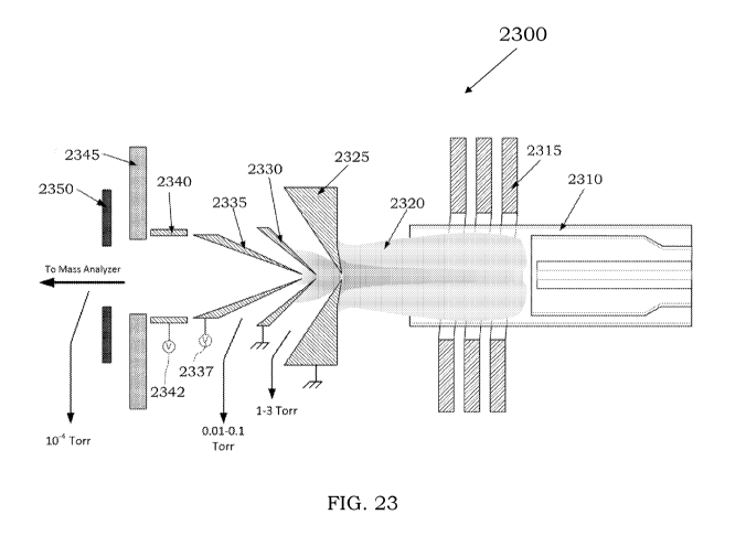
[0074] FIG. 23 is an illustration of a system including a torch, an induction
coil, an ion interface
and other components, in accordance with certain examples;
[0075] FIG. 24 is an illustration showing an ion interface where a lens is
positioned adjacent to
an ion guide, in accordance with some embodiments;
[0076] FIGS. 25A and 25B show a hyperskimmer cone and a ring lens placed in a
non-
conductive holder, in accordance with some embodiments;
[0077] FIGS. 26A and 26B show ion simulations for different systems, in
accordance with
certain examples;
[0078] FIGS. 27A and 27B show equipotential curves for different systems, in
accordance with
some configurations;
[0079] FIG. 28 shows a comparison of signal intensities using different
systems, in accordance
with certain embodiments;
[0080] FIG. 29 shows a system including a hyperskimmer and a ring lens, in
accordance with
certain embodiments; and
[0081] FIG. 30 is a cross-section of an ion interface, in accordance with
certain configurations.
[0082] It will be recognized by the person having ordinary skill in the art,
given the benefit of this
disclosure, that the sizes, dimensions and positioning of the components in
the figures are provided
merely for illustration and to provide a more user friendly description of the
technology. No
particular length, width, height or thickness is intended to be required
unless clearly specified in
connection with a particular embodiment. The dimensions provided below are
provided as
exemplary dimensions, and other suitable dimensions, shapes and features can
be present on the
various elements and in the ion interfaces.
[0083] DETAILED DESCRIPTION
CA 03170110 2022-08-03
WO 2021/156762 PCT/1B2021/050868
9
[0084] Certain illustrative configurations of ion interfaces are described
that can be used to
sample an incoming ion beam, focus the ions in the ion beam and provide the
focused ions to
another component. Embodiments of the ion interface may comprise desirable
attributes including,
but not limited to, enhanced transmission efficiency of ions, reduction in
space-charge effects,
higher sensitivities and the ability to optimize transmission of different
ions in real time by altering
voltages applies to different elements of the ion interface. Where the ion
interface is present in a
mass spectrometer, it can be considered, and is referred to in certain
instances, a mass spectrometer
interface. When certain embodiments of the ion interface are present in a mass
spectrometer,
increased sensitivity to ions across the mass range of the mass spectrometer
may be observed.
Additionally or alternatively, the signal to noise ratio across the mass range
of the mass
spectrometer may be increased.
[0085] In certain instances, in describing some of the illustrations herein,
the terms "downstream"
and "upstream" may be used for convenience. The position of one component
relative to another
component may be referenced by way of the direction of the incoming ion beam.
For example, if
an ion beam from an ionization source first enters the ion interface through a
sampler cone and
then encounters a skimmer cone, then the skimmer cone is downstream from the
sampler cone, and
the sampler cone is upstream of the skimmer cone.
[0086] In certain configurations, the ion interfaces described herein can be
used in analytical
instruments, in ion switches, in ion implantation devices, in ion beam
assisted molecular beam
epitaxy devices, to select or focus ions or particles from sputtering devices
used in physical and
chemical vapor deposition and in other devices that use a beam of ions or
particles. A generalized
block diagram is shown in FIG. IA where an incoming ion beam 105 impacts or
encounters an ion
interface 110. The ion interface 110 can be configured to receive or sample a
portion of the
incoming ion beam 105, e.g., to extract some but not all ions in the incoming
ion beam, focus the
ions and then provide an ion output 115 to a downstream component (not shown).
The exact degree
to which the ions are sampled and/or focused may vary, for example, depending
on the nature of
the ions in the incoming ion beam 105, the exact type and number of components
in the ion
interface 110 and the desired ion output 115. For example and referring to
FIG. 1B, an ion interface
130 can be configured to provide an ion output 135 from an incoming ion beam
125 to a surface
of a substrate 140. The ions provided to the substrate 140 can be used to
eject electrons or other
material from the substrate 140 or may implant ions on or in the surface of
the substrate 140. In
another configuration and referring to FIG. 1C, an ion interface 160 can be
used in a mass
spectrometer to provide an ion output 165 from an incoming ion beam 155 to a
downstream mass
spectrometer (MS) component 170. For example, the ion interface 160 may
comprise two or more
elements that can be used to sample and/or focus the ions in the incoming beam
155 to provide the
CA 03170110 2022-08-03
WO 2021/156762 PCT/1B2021/050868
ion output 165 to a downstream component present in a mass spectrometer. In
another
configuration and referring to FIG. 1D, an ion interface 180 can be used in a
mass spectrometer to
provide an ion output 185 from an incoming ion beam 175 directly to an ion
guide/deflector 190.
For example, it may be desirable to provide the ion output 185 directly to an
ion guide/deflector
190 without using any intervening components, e.g., a collision cell, between
the interface 180 and
the ion guide/deflector. In some instances, the ion interfaces 110, 130, 160,
and 180 may comprise
one or more cones and one or more cylindrical lenses as noted in more detail
herein. However, the
components of ion interfaces of some embodiments are not limited to these
particular components.
[0087] In certain embodiments, an ion interface may comprise two or more
elements as illustrated
in FIG. 2A. A member or element 200 comprises a body 210 and an orifice 220.
Another member
or element 250 comprises a body 260 and an orifice 270. While shown as two-
dimensional in FIG.
2A, the element 200 and the element 250 are typically three-dimensional and
may adopt various
shapes and geometries as noted below. In use of the ion interface of FIG. 2A,
an incoming ion
beam (not shown) can be incident on the surface 212 of the body 210. A portion
of the incoming
ion beam enters into the orifice 220 and is provided to the downstream element
250 through the
orifice 220 at a side or end 214 of the body 210. As noted in more detail
below, the element 250
can receive a non-zero voltage to focus the received ions prior to providing
them to a downstream
component. In certain embodiments, the element 200 may be a terminal element
or a terminal cone,
e.g., a hyperskimmer cone. Reference to a terminal cone refers to the cone
being the last cone
present in the interface, e.g., the cone which is furthest downstream from the
entrance of the ion
interface relative to other cones that may be included in the interface (but
not necessarily the
furthest downstream component of the interface). The exact configuration of
the element 200 may
vary, and in some instances, the element 200 may comprise shapes other than
conical shapes
including, for example, disc shapes, elongated discs, asymmetric discs,
spherical shapes, prolate
spheroid shapes and other shapes. The element 250 may be a lens such as a
cylindrical lens, e.g.,
a ring lens that can be used to focus received ions from the element 200 prior
to providing them to
the downstream component. The materials used for the element 200 and element
250 may also
vary depending on the nature of the incoming ion beam. Where high temperate
ion beams are
present, e.g., ion beams from an inductively coupled plasma, the element 200
and/or element 250
may comprise a metal such as, for example, nickel, copper, titanium, platinum,
palladium, silver,
gold or other metals. In some instances, the element 200 may desirably be
electrically conductive.
In other examples, the element 200 may be thermally conductive. In additional
configurations, the
element 200 may be electrically conductive and thermally conductive. Various
specific
configurations and materials for the elements 200, 250 are discussed in more
detail below.
CA 03170110 2022-08-03
WO 2021/156762 PCT/1B2021/050868
11
[0088] In certain embodiments, an inner diameter 275 of the orifice 270 of the
element 250 may
be greater than or equal to an outer diameter of the orifice 220. For example,
the inner diameter
275 may be larger than the outer diameter 225 or the same as the outer
diameter 225 as desired.
While the exact dimensions may vary, the outer diameter of the element 200 may
vary from about
0.5 cm to about 3 cm or about 1 cm to about 2.5 cm. The inner diameter of the
element 200 can
vary from about 0.75 cm to about 2.75 cm or about 1 cm to about 2.6 cm, though
other dimensions
are also possible. In some examples, the element 250 is positioned directly
adjacent to the element
200 such that no intervening physical components or structures are present
between them. While
the exact longitudinal spacing between the element 200 and the element 250 may
vary, illustrative
spacing is from about 0.5 mm to about 10 mm or about 1 mm to about 5 mm. This
spacing can be
fixed or may be adjusted as desired.
[0089] In certain embodiments, the element 200 can be configured to receive a
non-zero voltage
from a voltage source as shown in FIG. 2B. For example, the voltage applied to
the element 200
from a voltage source 290 may be positive or negative but is generally not
zero, e.g., the element
200 is not electrically coupled to ground. Application of the voltage to the
element 200 provides
a charge on the element 200 that can be used to sample and/or focus ions.
Similarly, the element
250 can be configured to receive a non-zero voltage, e.g., a positive or a
negative voltage, from the
voltage source 290 so a charge is present on the element 250. In some
examples, the voltage
applied to the element 250 may be from a different voltage source (not shown).
The voltage source
290 may be a DC voltage source, an AC voltage source, an RF voltage source or
other sources. In
some configurations, a DC voltage is provided to each of the first element 200
and the second
element 250. If desired, different voltage sources that provide different
waveforms can be used to
provide a voltage to each of the element 200 and the element 250. The exact
voltage provided to
the different components can vary. For example, a negative voltage less than
zero to about -50
Volts can be applied to the element 200. Alternatively, a positive voltage
greater than zero and up
to about +30 Volts can be applied to the element 200. A negative voltage less
than zero to about -
300 Volts can be applied to the element 250. Alternatively, a positive voltage
greater than zero
and up to about +50 Volts can be applied to the element 250. During use of the
ion interface, the
voltages provided to the elements 200 and 250 can independently be altered as
desired.
[0090] In certain examples, the voltages applied to each of the element 200
and the element 250
may vary. Several possible configurations are shown in FIGS. 3A-3C. An element
A 310 may be
configured similar to element 200. Element B 320 can be configured similar to
element 250.
Referring to FIG. 3A, a positive voltage is applied to the element 310, and a
negative voltage is
applied to the element 320. For example, the positive voltage applied to the
element 310 can focus
the incoming ions toward the element 310. As ions pass through an orifice of
the element 310, they
CA 03170110 2022-08-03
WO 2021/156762 PCT/1B2021/050868
12
can be quickly accelerated out of the element 310 (which also prevents ion
expansion that can
result in more lost ions and lower throughput). The negative voltage applied
to the element 320
can act to pull ions out of the element 310 before expansion due to the space-
charge effects can
occur. The exact magnitude of the voltages applied to each of the elements
310, 320 can vary. For
example, the positive voltage applied to the element 310 may vary from a
positive voltage greater
than zero to a positive voltage of about +30 Volts. The negative voltage
applied to the element
320 may vary from a negative voltage less than zero to a negative voltage of
about -300 Volts.
[0091] Referring now to FIG. 3B, the element 310 and the element 320 are each
positively
charged. In certain embodiments, the voltage applied to the element 320 may be
slightly more
positive than the voltage applied to the element 310, e.g., +V2 > +VI. For
easy to ionize samples,
e.g., potassium, sodium, etc., application of the positive voltages to the
elements 310, 320 can act
to reduce overall background noise. For example, where analyte ions of
interest are present at low
amounts, e.g., a few parts per trillion, the configuration shown in FIG. 3B
may be desirable to
implement to detect these low ion levels. The exact magnitude of the positive
voltages applied to
each of the elements 310, 320 in FIG. 3B can vary. For example, the positive
voltage applied to
the element 310 may vary from a positive voltage greater than zero to a
positive voltage of about
+30 Volts. The positive voltage applied to the element 320 may vary from a
positive voltage
greater than zero to a positive voltage of about +50 Volts. As noted herein,
the element 320 may
be held at a slightly more positive voltage, e.g., +2, +3, +4, +5, +6, +7 or
+8 Volts more positive,
than the voltage applied to the element 310.
[0092] In certain examples, the voltages applied to the element 310 and the
element 320 can be
altered in real time using a processor 350 as shown in FIG. 3C. As noted
herein, the processor 350
can be a stand-alone processor or part of a controller or larger system used
to control other
components. The processor 350, for example, can control the voltage applied to
each of the
elements 310, 320 to alter the mode of operation of the device or system
comprising the elements
310, 320. For example, the processor 350 can be used to apply a positive
voltage to the element
310 and a negative voltage to the element 320 in a first mode and then switch
the voltage applied
to the element 320 to positive voltage in a second mode. This mode switching
can be performed
by the processor 350 without changing the other operating parameters of the
system, if desired, to
switch the mode in real time.
[0093] In some embodiments, the element 200 can be configured as a skimmer
cone. Referring
to FIG. 4A, a side view of a skimmer cone 400 is shown that comprises a body
410 and an orifice
420. The cone opening angle 0 of the skimmer cone may vary. For example, where
the skimmer
cone is configured as a hyperskimmer cone that can receive a positive voltage,
the opening angle
0 of the hyperskimmer cone may be less than an opening angle of an upstream
cone, e.g., an
CA 03170110 2022-08-03
WO 2021/156762 PCT/1B2021/050868
13
upstream sampler cone or an upstream skimmer cone. In some examples, the cone
opening angle
may vary from about 35 degrees to about 45 degrees. The exact dimensions of
the cone 400 may
vary, and illustrative dimensions include a cone height of about 10 mm to
about 15 mm and a cone
radius of about 6 mm to about 9 mm. illustrative cone surface areas are about
350 mm2 to about
750 min2, and illustrative cone volumes may vary from about 350 mm3 to about
1200 mm3. The
diameter of the orifice 420 of the cone 400 may vary from about 0.5 mm to
about 1.5 mm. The
shape of the orifice 420 may vary and may be circular, elliptical or have
other geometric shapes.
If desired, more than a single opening or orifice may be present in the body
410 of the cone 400.
The cone 400 can be produced from various materials. In some examples, the
material used to
produce the cone 400 is electrically conductive. In other examples, the
material used to produce
the cone 400 is thermally conductive. In additional examples, the material
used to produce the cone
400 is electrically conductive and thermally conductive. In certain
configurations, the cone 400
may comprise one or more of nickel, copper, titanium, platinum, palladium,
silver, gold or other
metals. In certain embodiments, the cone 400 may be a hyperskimmer that can be
used as part of
a system that can reduce the overall pressure in smaller steps and provide
less dispersion of the ion
beam. The hyperskimmer is typically used with one or more upstream cones that
is positioned
closer to an ionization source than the hyperskimmer. Various configurations
using two or more
cones are discussed further below.
[0094] In certain examples and referring to FIG. 4B, the cone 400 can be
electrically coupled to
a voltage source 450. For example, the voltage source 450 can be used to
provide a non-zero
voltage to the cone 400. In some examples, the non-zero voltage applied to the
cone 400 may be
positive. Where a positive voltage is used, the cone 400 can act to focus an
ion beam that enters
the cone through the orifice 420. The focused ion beam can then be provided to
a downstream
component. In some embodiments, the voltage applied to the cone 400 may vary
from a positive
voltage greater than zero to about +30 Volts. In other embodiments, the
voltage applied to the
cone may be negative, e.g., a negative voltage less than zero to about -50
Volts. The voltage can
be applied using a DC voltage source or other voltage source. Where multiple
cones are present,
the orifice shape of different cones can be the same or can be different.
[0095] In certain configurations, the element 250 can be configured as a
cylindrical lens such as,
for example, a ring lens. A side view of a cylindrical lens 500 is shown in
FIG. 5A. The cylindrical
lens 500 comprises a body 510 and an aperture 520. The exact length and width
of the body 510
and the diameter of the aperture 520 may vary. In some embodiments, the
diameter of the aperture
520 may be greater than a length of the body 510. The diameter of the aperture
520 is typically
fixed though adjustable diameter lenses could be used if desired. In some
examples, the cylindrical
lens comprises a length of about 5 mm to about 7 mm, and an outer diameter of
about 16 mm to
CA 03170110 2022-08-03
WO 2021/156762 PCT/1B2021/050868
14
about 19 mm. In certain configurations, the aperture 520 may comprise a
diameter of about 14
mm to about 16 mm. In some embodiments, the aperture-to-length ratio of the
cylindrical lens
may be 2.5 or less. For example, compared to a flat lens whose length or
height is small, the length
or height of a cylinder lens is large. In some examples, the aperture-to-
length ratio of the
cylindrical lens may be less than 2.2, less than 2.0 or even less than 1.5. As
the length of the
cylinder lens increases at a fixed aperture diameter, the diameter-to-length
ratio should decrease.
[0096] In certain configurations, the cylindrical lens 500 may be electrically
coupled to a voltage
source 550 as shown in FIG. 5B. For example, the voltage source 550 can be
used to provide a
non-zero voltage to the lens 500. In some examples, the non-zero voltage
applied to the lens 500
may be negative or positive. Where a negative voltage is applied to the lens
500, the lens 500 can
act to pull ions into the aperture 520 and focus them before providing the
focused ions to a
downstream component. The exact negative voltage used may vary from a negative
voltage less
than zero to a negative voltage of about -300 Volts, e.g., a negative voltage
of about -100 Volts to
-250 Volts can be used. Where a positive voltage is applied to the lens 500,
the lens can be used
to focus ions while at the same time reducing background noise. The exact
positive voltage applied
to the lens 500 may vary from a positive voltage greater than zero to a
positive voltage of about
+50 Volts. If desired, the voltage provided to the lens 500 may be changed
during operation of a
system comprising the lens 500. For example, a processor (not shown) can be
used to alter the
voltage provided to the lens 500 from positive to negative or from negative to
positive in real time
during operation of the system.
[0097] In certain embodiments, the exact materials used to produce the lens
may vary, and the
lens typically comprises one or more conductive materials such that
application of a non-zero
voltage to the lens can provide an electric field within the aperture 520 of
the lens. In some
embodiments, the lens may be produced from the same or similar materials as
used to produce the
other elements of the ion interface, e.g., the lens materials may comprise
nickel, copper, titanium,
platinum, palladium, silver, gold or other metals or conductive materials. If
desired, the lens may
be placed in a holder configured to receive the lens at one side and an
upstream element at another
side. The holder typically comprises a non-conductive material such that any
voltage applied to
the lens is not provided to the upstream element through the holder. The non-
conductive material
may be, for example, a glass, a plastic, a non-metal, a polymer or other
materials that are non-
conductive. The holder can retain the elements of the ion interface using a
friction fit, threads,
spring-loaded retainers, one or more external fasteners or other devices or
structures.
[0098] In certain configurations, the voltage received by the lens can be
configured to provide an
electric field with an inflection point. One illustration is shown in FIG. 6A,
where a ring lens 610
is shown. Equipotential lines with voltages V1-V4 are shown. In a typical
configuration where a
CA 03170110 2022-08-03
WO 2021/156762 PCT/1B2021/050868
negative potential is applied to the ring lens 610, the potential is more
positive toward a front
surface 612 of the ring lens 610, e.g., near VI and then decreases toward a
minimum within the
lens 610, e.g., V2 is more negative than VI. The voltage then can increase or
have a lower
magnitude negative potential moving toward the back surface 614 of the lens
610, e.g., V4 is less
negative than V3. In instances where a first element is used with the lens
610, the potential can be
positive on the first element and then decrease to the negative minimum within
or near the lens
610 and the become less positive as the ions exit the lens 610 toward the back
surface 614. The
absolute voltage difference from the front surface 612 of the lens 610 to the
minimum voltage or
inflection point may vary, for example, from about 50 Volts to about 150
Volts. In addition, the
minimum or inflection point need not be centralized within the aperture of the
lens 610 but could
instead be positioned closer to the front surface 612, the back surface 614 or
even in front of the
lens surface 612 or behind the lens surface 614. For example, FIG. 6B shows
another configuration
where the minimum occurs at V6 closer to the front 632 of the lens 630, e.g.,
V6 is more negative
than V5 and the voltage can increase (become less negative) as the ions move
from V7 to Vs and
V9 toward the back surface 634 of the lens 630. The exact field shape and
pattern can vary as
desired. As noted herein, the field can be used to accelerate ions out of an
upstream element toward
the lens where they can be focused or squeezed before exiting the lens. The
voltage applied to the
lenses 610, 630 can be a DC voltage or other voltage sources can be used if
desired. In addition,
the voltage applied to the lenses 610, 630 can ab altered during use of the
lenses 610, 630.
[0099] In certain embodiments, an element such as a cone can be used with
another element such
as a lens, for example, to increase ion transmission efficiency, reduce
background noise, reduce
space-charge effects, etc. An illustration is shown in FIG. 7A where an ion
interface 700 comprises
a cone 710 comprising an entrance orifice 720 and an exit orifice 725. The
interface 700 also
comprises a cylindrical lens 740 comprising an aperture 745. In some
instances, a diameter of the
aperture 745 of the lens 740 may be greater than or equal to a diameter of the
exit orifice 725. Ions
in an ion beam are first incident on the cone 710, and certain ions pass
through the entrance orifice
720. The cone 710 can act to pull the ions into the cone 710 and can focus the
ions and provide
them to the lens 740. The lens 740 may also focus the ions before providing
them to a downstream
component. For example and referring to FIG. 7B, a voltage source 750 can be
used to apply a
non-zero voltage to each of the cone 710 and the lens 740. For example, a
positive voltage greater
than zero to a positive voltage of about +30 Volts can be provided to the cone
710 from the voltage
source 750. If desired, however, a negative voltage between -50 Volts to 0
Volts can be applied to
the cone 710. A negative or a positive voltage can be provided to the lens 740
from the voltage
source 750. Where a negative voltage is applied to the lens 740, the negative
voltage can vary
from a negative voltage less than zero to a negative voltage of about -300
Volts. Where a positive
CA 03170110 2022-08-03
WO 2021/156762 PCT/1B2021/050868
16
voltage is applied to the lens 740, the positive voltage can be a positive
voltage greater than zero
to a positive voltage of about +50 Volts. The voltages are typically provided
using a DC voltage
source though other sources can be used. In another configuration, two
separate voltage sources
can be used to provide a voltage to the cone 710 and the lens 740. Referring
to FIG. 7C, a first
voltage source 760 can provide a first non-zero voltage to the cone 710, and a
second voltage
source 770 can provide a second non-zero voltage to the lens 740. The voltage
source 760 can
apply a positive voltage to the cone 710, e.g., can provide a positive voltage
greater than zero up
to about +30 Volts, or can apply a negative voltage to the cone 710. The
voltage source 770 can
apply a positive voltage or a negative voltage to the lens 740, e.g., a
voltage of about -300 Volts
up to about +50 Volts. The materials of the cone 710 may be, for example, any
of those materials
described in reference to FIGS. 4A and 4B.
[00100] In certain examples, an element such as a cone can be used with an
additional element or
additional cone to sample and/or focus ions. One illustration is shown in FIG.
8A, where an ion
interface 800 comprises a first cone 810 and a second cone 830. In this
illustration, the second
cone 830 would be considered the terminal cone. The first cone 810 comprises a
first orifice 820
that can receive ions. The second cone 830 comprises a second orifice 840 that
can receive ions.
As shown in FIG. 8B, the first cone 810 can be configured to electrically
couple to ground, and the
second cone 830 can be configured to receive a non-zero voltage from a voltage
source 850. For
example, the second cone 830 can be configured to receive a positive voltage
from the source 850,
e.g., a voltage greater than zero volts up to about +30 Volts, or can receive
a negative voltage. The
cone opening angle of the cone 830 is typically less than a cone opening angle
of the cone 810.
The diameter of the first orifice 820 may vary from about 0.9 mm to about 1.3
mm, and the diameter
of the second orifice 840 may vary from about 0.5 mm to about 1.1 mm. The
orifice shapes of the
cones 810, 830 can be the same or can be different, e.g., circular,
elliptical, etc. In some examples,
a front surface of the cone 810 can be spaced a distance of about 2 mm to
about 5 mm from a front
surface of the cone 830
[00101] In use of the cones 810, 830, ions from an ion source are typically
incident first on the
cone 810. A portion of the ions can be sampled through the orifice 820 and
provided to the
downstream cone 830. The charge on the cone 830 can act to pull the ions
through the orifice 840.
A portion of those ions may pass through the orifice 840 of the cone 830 and
can be focused or
accelerated out of the cone 830 using a suitable voltage provided to the cone
830. The cones 810,
830 may comprise the same or different materials, e.g., each of the cones 810,
830 may
independently comprise nickel, copper, titanium, platinum, palladium, silver,
gold or other metals.
In some instances, each of the cones 810, 830 comprises nickel. If desired,
the cone 810 could be
produced from a non-conductive material, so the cone 810 need not be
electrically grounded.
CA 03170110 2022-08-03
WO 2021/156762 PCT/1B2021/050868
17
[00102] In some configurations, two or more elements, e.g., two or more cones,
can be used in
combination with a cylindrical lens as shown in FIG. 9A. The ion interface 900
comprises a first
cone 910 with a first orifice 920 that can receive ions, a second cone 930
with a second orifice 940
that can receive ions, and a cylindrical lens 960 with an aperture 970 that
can receive ions. In this
illustration, the cone 930 can be considered a terminal cone. As shown in FIG.
9B, the first cone
910 can be configured to electrically couple to ground, and the second cone
930 can be configured
to receive a non-zero voltage from a voltage source 980. For example, the
second cone 930 can
be configured to receive a positive voltage from the source 980, e.g., a
voltage greater than zero
volts up to about +30 Volts, or can receive a negative voltage. The lens 960
can be configured to
receive a positive or negative voltage from the voltage source 980, e.g., a
voltage between about -
250 Volts to about + 50 Volts. Where the lens 960 receives a positive voltage,
the positive voltage
is typically more positive than the positive voltage applied to the cone 930,
e.g., about +1, +2, +3,
+4, +5, +6, +7 or +8 Volts more positive. If desired, two different voltage
sources can be used to
provide a voltage to the cone 930 and the lens 960. For example and referring
to FIG. 9C, a first
voltage source 985 is electrically coupled to the cone 930, and a second
voltage source 990 is
electrically coupled to the lens 960. The cone opening angle of the cone 930
is typically less than
a cone opening angle of the cone 910. The diameter of the first orifice 920
may vary from about
0.6 mm to about 1.2 mm, and the diameter of the second orifice 940 may vary
from about 0.8 mm
to about 1.2 mm. The diameter of the aperture 970 is typically equal to or
greater than the outer
diameter of the cone opening at the end of the cone 930 that is adjacent to
the lens 960. The orifice
shapes of the cones 910, 930 can be the same or can be different, e.g.,
circular, elliptical, etc. If
desired, the lens 960 can be placed immediately adjacent to the cone 930
without any intervening
components or structures between them. Further, the lens 960 and the cone 930
can be held
together using a coupler or connector as desired. In some examples, a front
surface of the cone
910 can be spaced a distance of about 2 mm to about 5 mm from a front surface
of the cone 930.
The front surface of the cone 930 can be spaced about 15 mm to about 25 mm
from a front surface
of the lens 960.
[00103] In use of the cones 910, 930 and the lens 960, ions from an ion source
are typically incident
first on the cone 910. A portion of the ions can be sampled through the
orifice 920 and provided
to the downstream cone 930. A portion of those ions may pass through the
second orifice 940 of
the cone 930 and can be focused or accelerated out of the cone 930 using a
suitable voltage
provided to the cone 930. A suitable voltage can be provided to the lens 960
to increase
acceleration of the ions out of the cone 930. The lens 960 can focus or
squeeze the ions as they
pass through the aperture 970 of the lens 960. The ions can then exit the lens
960 as a focused
beam and can be provided to a downstream component. The cones 910, 930 may
comprise the
CA 03170110 2022-08-03
WO 2021/156762 PCT/1B2021/050868
18
same or different materials, e.g., each of the cones 910, 930 may
independently comprise nickel,
copper, titanium, platinum, palladium, silver, gold or other metals. In some
instances, each of the
cones 910, 930 comprises nickel. If desired, the cone 910 could be produced
from a non-
conductive material so the cone 910 need not be electrically grounded. As
noted herein, the lens
960 may comprise an electric field with a minimum or inflection point within
the aperture 970, in
front of the aperture 970 or behind the aperture 970. The lens 960 can be
produced from those
materials described in connection, for example, with the lens shown in FIGS.
5A and 5B.
[00104] In certain embodiments, an ion interface comprising a cylindrical lens
can be used with
one or more uncharged elements or cones. Referring to FIG. 10A, an ion
interface 1000 comprises
a cone 1010 comprising a body 1015 and an orifice 1020. The ion interface 1000
also comprises
a cylindrical lens 1030 comprising an aperture 1040. A diameter of the
aperture 1040 can be
greater than or equal to an outer diameter of the cone 1010. As shown in FIG.
10B, the cone 1010
can be electrically coupled to ground, and the lens 1030 can be electrically
coupled to a voltage
source 1050 which can provide a non-zero voltage to the lens 1030. For
example, the lens 1030
can be configured to receive a positive or negative voltage from the voltage
source 1050, e.g., a
voltage between about -250 Volts to about + 50 Volts. A front surface of the
cone 1010 can be
spaced about 15 mm to about 25 mm from a front surface of the lens 1030.
[00105] In use of the cone 1010 and the lens 1030, ions from an ion source are
typically incident
first on the cone 1010. A portion of the ions can be sampled through the
orifice 1020 and provided
to the downstream lens 1030. A suitable voltage can be provided to the lens
1030 to increase
acceleration of the ions out of the electrically grounded cone 1010 and can
focus or squeeze the
ions as they pass through the aperture 1040 of the lens 1030. The ions can
then exit the lens 1030
as a focused beam and can be provided to a downstream component. The cone 1010
may comprise
nickel, copper, titanium, platinum, palladium, silver, gold or other metals.
If desired, the cone
1010 could be produced from a non-conductive material so the cone 1010 need
not be electrically
grounded. As noted herein, the lens 1030 may comprise an electric field with a
minimum or
inflection point within the aperture 1040, in front of the aperture 1040 or
behind the aperture 1040.
The lens 1030 can be produced from those materials described in connection
with the lens shown
in FIGS. 5A and 5B. The orifice shapes of the cone 1010 can be, for example,
circular, elliptical,
or other shapes.
[00106] In certain configurations, an ion interface may comprise more than two
elements, e.g.,
more than two cones. For example and referring to FIG. 11A, an ion interface
is shown that
comprises a first element or cone 1110 with a first orifice 1115, a second
element or cone 1120
with a second orifice 1125, and a third element or cone 1130 with a third
orifice 1135. An incoming
ion beam 1105 is shown for reference. The incoming ion beam 1105 first
encounters the first cone
CA 03170110 2022-08-03
WO 2021/156762 PCT/1B2021/050868
19
1110. A portion of the incoming ion beam 1105 passes through the first orifice
1115 and is
provided to the downstream second element 1120. The second element or cone
1120 samples the
ions received from the first element or cone 1110 and provides a certain
amount of the ions to the
downstream third element 1130 through the second orifice 1125. The third
element or cone 1130
receives the ions through the third orifice 1135 and can be used to focus the
ions prior to providing
them to a downstream component. In some examples as shown in FIG. 11B, the
third element or
cone 1130 can be electrically coupled to a voltage source 1150 that can
provide a positive voltage
(or a negative voltage) to the third element or cone 1130. For example, the
voltage source 1150
can be used to provide a positive voltage to the third element or cone 1130,
e.g., a positive voltage
of greater than zero Volts up to about +30 Volts. In some configurations as
shown in FIG. 11C,
the first element or cone 1110 can be configured to electrically couple to
ground. In other
configurations as shown in FIG. 11D, the second element or cone 1120 can be
configured to
electrically couple to ground. In additional configurations as shown in FIG.
11E, both the second
element or cone 1120 and the third element or cone 1130 can be configured to
electrically couple
to ground. If desired, a common ground can be used to electrically couple the
second element
1120 and the third element 1130 to ground. A front surface of the cone 1110
can be spaced about
mm to about 12 mm from a front surface of the cone 1120. A front surface of
the cone 1120 can
be spaced about 2 mm to about 5 mm from a front surface of the cone 1130.
[00107] In certain embodiments, the cones 1110, 1120, 1130 may comprise the
same or different
materials, e.g., each of the cones 1110, 1120, 1130 may independently comprise
nickel, copper,
titanium, platinum, palladium, silver, gold or other metals. In some
instances, each of the cones
1110, 1120, 1130 comprises nickel. If desired, the cones 1110 and 1120 each
could be produced
from a non-conductive material so the cones 1110 and 1120 need not be
electrically grounded.
[00108] In other configurations, an ion interface may comprise more than two
elements or cones
in combination with a fourth element such as, for example, a cylindrical lens.
Referring to FIG.
12A, an ion interface is shown that comprises a first element or cone 1210
with a first orifice 1215,
a second element or cone 1220 with a second orifice 1225, a third element or
cone 1230 with a
third orifice 1235, and a fourth element 1240 with an aperture 1245. An
incoming ion beam 1205
is shown for reference. The incoming ion beam 1205 first encounters the first
cone 1210. A
portion of the incoming ion beam 1205 passes through the first orifice 1215
and is provided to the
downstream second element 1220. The second element or cone 1220 samples the
ions received
from the first element or cone 1210 and provides a certain amount of the ions
to the downstream
third element 1230 through the second orifice 1225. The third element or cone
1230 receives the
ions through the third orifice 1235 and can be used to focus the ions prior to
providing them to a
downstream fourth element 1240. The fourth element 1240 can be configured, for
example, as a
CA 03170110 2022-08-03
WO 2021/156762 PCT/1B2021/050868
cylindrical lens comprising an aperture 1245. In some examples as shown in
FIG. 12B, the third
element or cone 1230 can be electrically coupled to a voltage source 1250 that
can provide a
positive voltage (or a negative voltage) to the third element or cone 1230.
For example, the voltage
source 1250 can be used to provide a positive voltage to the third element or
cone 1230, e.g., a
positive voltage of greater than zero Volts up to about +30 Volts. In other
configurations, a voltage
source 1255 can be electrically coupled to the fourth element 1240 as shown in
FIG. 12C. For
example, the voltage source 1255 can provide a non-zero voltage to the fourth
element 1240, e.g.,
can provide a negative or positive voltage that may range from about -250
Volts to about +50
Volts. In certain configurations as shown in FIG. 12D, a voltage source 1265
can provide a non-
zero voltage to each of the third element 1230 and the fourth element 1240.
While not shown, two
separate voltage sources could be used instead. In some instances, the voltage
source 1265 can
provide a non-zero voltage to the third element 1230, e.g., a positive voltage
greater than zero and
up to about +30 Volts or a negative voltage, and can provide a non-zero
voltage to the fourth
element 1240, e.g., a negative voltage or positive voltage that can range from
about -250 Volts up
to about +50 Volts. In some instances where a positive voltage is provided to
the fourth element
1240 from the voltage source 1265, the positive voltage provided to the fourth
element 1240 may
be more positive than the positive voltage provided to the third element 1230.
[00109] In some configurations, the second element 1220 may be configured to
electrically couple
to ground as shown in FIG. 12E. In other configurations, the first element may
be configured to
electrically couple to ground as shown in FIG. 12F. In other embodiments, each
of the first element
1210 and the second element 1220 may be configured to electrically couple to
ground as shown in
FIG. 12G. The cones 1210, 1220, 1230 may comprise the same or different
materials, e.g., each
of the cones 1210, 1220, 1230 may independently comprise nickel, copper,
titanium, platinum,
palladium, silver, gold or other metals. In some instances, each of the cones
1210, 1220, 1230
comprises nickel. If desired, the cones 1210 and 1220 each could be produced
from a non-
conductive material so the cones 1210 and 1220 need not be electrically
grounded. The lens 1240
can be produced from any of those materials described in reference to the lens
shown in FIGS. 5A
and 5B. A front surface of the cone 1210 can be spaced about 5 mm to about 12
mm from a front
surface of the cone 1220. A front surface of the cone 1220 can be spaced about
2 mm to about 5
mm from a front surface of the cone 1230. Th front surface of the cone 1230
can be spaced about
15 mm to about 25 mm from a front surface of the lens 1240. The base of the
cone 1230 may
comprise a diameter of about 12 mm to about 18 mm, and the diameter of the
aperture 1245 of the
lens 1240 may equal to or greater than the diameter of the base of the cone
1230. The lens 1240
may comprise a length of about 4 mm to about 10 mm.
CA 03170110 2022-08-03
WO 2021/156762 PCT/1B2021/050868
21
[00110] In certain configurations, an ion interface comprising two or more
individual elements can
be used to provide ions to a surface or other components as shown in the block
diagrams of FIGS.
13A-13D. Referring to FIG. 13A, the ion interface may comprise a first element
1302 and a second
element 1303 that can sample an incoming ion beam 1301 and provide focused
ions 1304 to a
surface 1305. In some examples, the first element 1302 may be configured to
electrically couple
to ground. In other examples, the first element 1302 may be configured to
receive a non-zero
voltage, e.g., a voltage between -50 Volts up to about +30 Volts. The second
element 1303 can be
configured to receive a non-zero voltage, e.g., a voltage that can vary from -
300 Volts up to +50
Volts. In some configurations, the positive voltage provided to the second
element 1303 may be
more positive than the positive voltage provided to the first element 1302. In
certain examples,
the first element 1302 is directly coupled to the second element 1303 without
any intervening
components. If desired, a connector, holder or coupler (not shown) can be used
to hold the first
element 1302 and the second element 1303 in place. In some instances, the
first element 1302 can
be configured as a skimmer cone or hyperskimmer cone, and the second element
1303 can be
configured as a cylindrical lens, e.g., a ring lens. The first element 1302
and the second element
1303 can provide an ion beam 1304 to the surface 1305 to implant the ions in
the surface 1305, to
eject ions from the surface 1305, to etch the surface 1305 or for other uses.
[00111] Referring to FIG. 13B, an ion interface may comprise a first element
1307 and a second
element 1308 that can sample an incoming ion beam 1306 and provide focused
ions 1309 to a
downstream component 1310. In certain embodiments, the first element 1307 can
be configured
to electrically couple to ground. In other examples, the first element 1307
may be configured to
receive a non-zero voltage, e.g., a voltage between -50 Volts up to about +30
Volts. In some
configurations, the second element 1308 can be configured to receive a non-
zero voltage, e.g., a
voltage that can vary from -300 Volts up to +50 Volts. In some configurations,
the positive voltage
provided to the second element 1308 may be more positive than the positive
voltage provided to
the first element 1307. In certain examples, the first element 1307 is
directly coupled to the second
element 1308 without any intervening components. If desired, a connector,
holder or coupler (not
shown) can be used to hold the first element 1307 and the second element 1308
in place. In some
examples, the first element 1307 can be configured as a skimmer cone or
hyperskimmer cone, and
the second element 1308 can be configured as a cylindrical lens, e.g. a ring
lens. As noted herein,
the lens can be configured to provide an equipotential inflection point if
desired.
[00112] In some examples, the first element 1307 and the second element 1308
can provide an ion
beam 1309 to a downstream component 1310 as shown in FIG. 13B. For example,
the downstream
component 1310 can be an ion gun, an ion trap or other devices. In some
configurations, the
downstream component 1310 can be a mass spectrometer component 1315 as shown
in FIG. 13C
CA 03170110 2022-08-03
WO 2021/156762 PCT/1B2021/050868
22
and as discussed in more detail below. In other configurations, the downstream
component 1310
can be an ion guide 1320 as shown in FIG. 13D. If desired, the downstream
component 1310, e.g.,
the ion guide 1320, can be directly coupled to the second element 1308 such
that no components
are positioned between the second element 1308 and the downstream component
1310.
Alternatively, ion optics may be present between the second element 1308 and
the ion guide 1320
to further focus the beam 1309.
[00113] In certain configurations, an ion interface comprising three or more
individual elements
can be used to provide ions to a surface or other components as shown in the
block diagrams of
FIGS. 14A-14D. Referring to FIG. 14A, the ion interface may comprise a first
element 1402, a
second element 1403, and a third element 1404 that can sample an incoming ion
beam 1401 and
provide focused ions 1405 to a surface 1406. In some examples, the first
element 1402 can be
configured to electrically couple to ground. In certain embodiments, the
second element 1403 may
be configured to receive a non-zero voltage, e.g., a voltage between -50 Volts
up to about +30
Volts. The third element 1404 can be configured to receive a non-zero voltage,
e.g., of voltage
that can vary from -300 Volts up to +50 Volts. In some configurations, the
positive voltage
provided to the third element 1404 may be more positive than the positive
voltage provided to the
second element 1403. In certain examples, the second element 1403 is directly
coupled to the third
element 1404 without any intervening components. If desired, a connector,
holder or coupler (not
shown) can be used to hold the second element 1403 and the third element 1404
in place. In some
instances, the first element 1402 can be configured as a sampler cone or a
skimmer cone, the second
element 1403 can be configured as a skimmer cone or hyperskimmer cone, and the
third element
1404 can be configured as a cylindrical lens, e.g., a ring lens. The first
element 1402, the second
element 1403, and the third element 1404 can provide a focused ion beam 1405
to the surface 1406
to implant the ions in the surface 1406, to eject ions from the surface 1406,
to etch the surface 1406
or for other uses.
[00114] Referring to FIG. l 4B, an ion interface may comprise a first element
1412, a second
element 1413, and a third element 1414 that can sample an incoming ion beam
1411 and provide
focused ions 1415 to a downstream component 1420. In some examples, the first
element 1412
can be configured to electrically couple to ground. In other examples, the
second element 1413
can be configured to receive a non-zero voltage, e.g., a voltage between -50
Volts up to about +30
Volts. In other embodiments, the third element 1414 can be configured to
receive a non-zero
voltage, e.g., a voltage that can vary from -300 Volts up to +50 Volts. In
some configurations, the
positive voltage provided to the third element 1414 may be more positive than
the positive voltage
provided to the second element 1413. In certain examples, the second element
1413 is directly
coupled to the third element 1414 without any intervening components. If
desired, a connector,
CA 03170110 2022-08-03
WO 2021/156762 PCT/1B2021/050868
23
holder or coupler (not shown) can be used to hold the second element 1413 and
the third element
1414 in place. In some instances, the first element 1412 can be configured as
a sampler cone or a
skimmer cone, the second element 1413 can be configured as a skimmer cone or
hyperskimmer
cone, and the third element 1414 can be configured as a cylindrical lens,
e.g., a ring lens. As noted
herein, the lens can be configured to provide an equipotential inflection
point if desired.
[00115] In some configurations, the first element 1412, the second element
1413, and the third
element 1414 can provide an ion beam 1415 to the downstream component 1420 as
shown in FIG.
14B. For example, the downstream component 1420 can be an ion gun, an ion trap
or other
devices. In some configurations, the downstream component 1420 is a mass
spectrometer
component 1430 as shown in FIG. 14C and as discussed in more detail below. In
other
configurations, the downstream component can be an ion guide 1440 as shown in
FIG. 14D. If
desired, the downstream component 1420, e.g., the ion guide 1440, can be
directly coupled to the
third element 1414 such that no components are positioned between the third
element 1414 and
the downstream component 1420. Alternatively, ion optics can be present
between the third
element 1414 and the ion guide 1440 to further focus the ion beam 1415.
[00116] In certain configurations, an ion interface comprising four or more
individual elements
can be used to provide ions to a surface or other components as shown in the
block diagrams of
FIGS. 15A-15D. Referring to FIG. 15A, the ion interface may comprise a first
element 1502, a
second element 1504, a third element 1506, and a fourth element 1508 that can
sample an incoming
ion beam 1501 and provide focused ions 1509 to a surface 1510. In some
examples, the first
element 1502 can be configured to electrically couple to ground. In other
examples, the second
element 1504 can be configured to electrically couple to ground. In certain
embodiments, the third
element 1506 may be configured to receive a non-zero voltage, e.g., a voltage
between -50 Volts
up to about +30 Volts. In certain examples, the fourth element 1508 can be
configured to receive
a non-zero voltage, e.g., of voltage that can vary from -300 Volts up to +50
Volts. In some
configurations, the positive voltage provided to the fourth element 1508 may
be more positive than
the positive voltage provided to the third element 1506. In certain examples,
the third element
1506 is directly coupled to the fourth element 1508 without any intervening
components. If
desired, a connector, holder or coupler (not shown) can be used to hold the
third element 1506 and
the fourth element 1508 in place. In some instances, the first element 1502
and the second element
1504 can each be configured as a sampler cone or a skimmer cone, the third
element 1506 can be
configured as a skimmer cone or hyperskimmer cone, and the fourth element 1508
can be
configured as a cylindrical lens, e.g., a ring lens. The first element 1502,
the second element 1504,
the third element 1506 and the fourth element 1508 can provide an ion beam
1509 to the surface
CA 03170110 2022-08-03
WO 2021/156762 PCT/1B2021/050868
24
1510 to implant the ions in the surface 1510, to eject ions from the surface
1510, to etch the surface
1510 or for other uses.
[00117] Referring to FIG. 15B, an ion interface may comprise a first element
1512, a second
element 1514, a third element 1516 and a fourth element 1518 that can sample
an incoming ion
beam 1511 and provide focused ions 1519 to a downstream component 1520. In
some examples,
the first element 1512 can be configured to electrically couple to ground. In
other examples, the
second element 1514 can be configured to electrically couple to ground. In
additional examples,
the third element 1516 can be configured to receive a non-zero voltage, e.g.,
a voltage between -
50 Volts up to about +30 Volts. In other embodiments, the fourth element 1518
can be configured
to receive a non-zero voltage, e.g., a voltage that can vary from -300 Volts
up to +50 Volts. In
some configurations, the positive voltage provided to the fourth element 1518
may be more
positive than the positive voltage provided to the third element 1516. In
certain examples, the third
element 1516 is directly coupled to the fourth element 1518 without any
intervening components.
If desired, a connector, holder or coupler (not shown) can be used to hold the
third element 1516
and the fourth element 1518 in place. In some instances, each of the first
element 1512 and the
second element 1514 can be configured as a sampler cone or a skimmer cone, the
third element
1516 can be configured as a skimmer cone or hyperskimmer cone, and the fourth
element 1518
can be configured as a cylindrical lens, e.g. a ring lens. As noted herein,
the lens can be configured
to provide an equipotential inflection point if desired.
[00118] In some configurations, the first element 1512, the second element
1514, the third element
1516 and the fourth element 1518 can provide an ion beam 1519 to a downstream
component 1520
as shown in FIG. 15B. For example, the downstream component 1520 can be an ion
gun, an ion
trap or other devices. In some configurations, the downstream component 1520
is a mass
spectrometer component 1530 as shown in FIG. 15C and as discussed in more
detail below. In
other configurations, the downstream component 1520 can be an ion guide 1540
as shown in FIG.
15D. If desired, the downstream component 1520, e.g., the ion guide 1540, can
be directly coupled
to the fourth element 1518 such that no components are positioned between the
fourth element
1518 and the downstream component 1520. Alternatively, ion optics may be
present between the
fourth element 1518 and the ion guide 1540 to further focus the beam 1519.
[00119] While ion interfaces that comprise two, three or four elements are
shown in FIGS. 13A-
15D, it will be recognized by the person having ordinary skill in the art,
given the benefit of this
disclosure, that more than four individual elements may also be present in an
ion interface if
desired. Further, the exact cone opening angles, materials, sizes and
dimensions of the elements
and the orifices and apertures may vary as desired.
CA 03170110 2022-08-03
WO 2021/156762 PCT/1B2021/050868
[00120] In certain embodiments, the ion interfaces described herein can be
used with a sample
introduction device as shown in FIG. 16A. For example, a sample introduction
device 1610 can
be fluidically coupled to an ion interface 1620 so material can be provided
from the sample
introduction device 1610 to the ion interface 1620. In some instances, the
sample introduction
device 1610 may provide ions to the ion interface 1620 (FIG. 16B) for sampling
and/or focusing.
In other examples, the sample introduction device 1610 may be configured to
provide a liquid
sample or a gaseous sample. The ion interface 1620 can provide ions to a
downstream component
1625 as shown in FIG. 16C. In some instances, the downstream component can be
an ion guide
1630 (FIG. 16D), which can be directly positioned adjacent to the ion
interface 1620 without any
intervening components or structures. In other configurations, the ion
interface 1620 can provide
ions to a mass analyzer 1640 as shown in FIG. 16E. These components may also
be present in a
system which comprises a detector 1645 and a processor 1650 (FIG. 16F) that
can be used to
control the system. For example, the processor 1650 can be used to provide the
voltages to the
elements of the ion interface and/or alter the applied voltages in real time.
[00121] In some embodiments, the sample introduction device 1610 can be
fluidically coupled to
an ionization source 1615 as shown in FIG. 16B. The sample introduction device
1610 can provide
a fluid sample, e.g., a gas, liquid, etc., to the ionization source 1615,
which can ionize and/or
atomize the fluid sample and provide the ions/atoms to the downstream ion
interface 1620.
[00122] In some embodiments, the sample introduction device can be configured
as a nebulizer as
shown in FIG. 17. The nebulizer 1700 can be configured as an induction
nebulizer, a non-induction
nebulizer or a hybrid of the two. For example, concentric, cross flow,
entrained, V-groove, parallel
path, enhanced parallel path, flow blurring and piezoelectric nebulizers can
be used. In a simplified
form, the nebulizer 1700 comprises a tube or chamber 1702 in which a sample is
introduced
through an inlet 1706 or another tube 1704. A gas may be introduced into the
chamber 1702 to
entrain the introduced sample in the gas flow so the combination of gas and
sample can be provided
to an ionization source (or an ion interface) through an outlet 1703 of the
tube 1702. A pump 1710
may be present and fluidically coupled to the nebulizer 1700 to provide the
sample into the chamber
1702 through the inlet 1706. The gas typically is introduced into the
nebulizer 1700 at a different
port and can mix with the liquid sample before or after (or both) introduction
of the liquid sample
into the chamber 1702.
[00123] In certain embodiments, the sample introduction device 1610 can be
configured as a spray
chamber as shown in FIG. 18. The spray chamber 1800 generally comprises an
outer chamber or
tube 1810 and an inner tube 1820. The outer chamber 1810 comprises dual makeup
gas inlets
1812, 1814 and a drain 1818. The makeup gas inlets 1812, 1814 are typically
fluidically coupled
to a common gas source, though different gases could be used if desired. While
not required, the
CA 03170110 2022-08-03
WO 2021/156762 PCT/1B2021/050868
26
makeup gas inlets 1812, 1814 are shown as being positioned adjacent to an
inlet end 1811, though
they could instead be positioned centrally or toward an outlet end 1813. The
inner tube 1820 is
positioned adjacent to a nebulizer tip 1805 and comprises two or more
microchannels 1822, 1824
configured to provide a makeup gas flow to reduce or prevent droplets from
back flowing and/or
depositing on the inner tube 1820. The configuration and positioning of the
inner tube 1820
provides laminar flow at areas 1840, 1842 which acts to shield inner surfaces
of the outer chamber
1810 from any droplet deposition. The tangential gas flow provided by way of
gas introduction
into the spray chamber 1800 through the inlets 1812, 1814 acts to select
particles (or analyte
molecules) of a certain size range. The microchannels 1822, 1824 in the inner
tube 1820 also are
designed to permit the gas flows from the makeup gas inlets 1812, 1814 to
shield the surfaces of
the inner tube 1820 from droplet deposition. In certain examples, the
microchannels 1822, 1824
can be configured in a similar manner, e.g., have the same size and/or
diameter, whereas in other
configurations the microchannels 1822, 1824 may be sized or arranged
differently. In some
instances, at least two, three, four, five or more separate microchannels can
be present in the inner
tube 1820. The exact size, form and shape of the microchannels may vary and
each microchannel
need not have the same size, form or shape. In some examples, different
diameter microchannels
may exist at different radial planes along a longitudinal axis LI of the inner
tube to provide a
desired shielding effect. In certain examples, the inner tube 1820 is shown as
having a generally
increasing internal diameter along the longitudinal axis of the outer chamber
1810, though as noted
herein this dimensional change is not required. Some portion of the inner tube
1820 may be "flat"
or generally parallel with the longitudinal axis Li to enhance the laminar
flow, or in an alternative
configuration, some portion of the inner tube 1820 may generally be parallel
to the surface of the
outer tube 1810, at least for some length, to enhance laminar flow. The inner
diameter of the outer
chamber increases from the inlet end 1811 toward the outlet end 1813 up to a
point and then
decreases toward the outlet end 1813 such that the inner diameter of the outer
chamber 1810 is
smaller at the outlet end 1813 than at the inlet end 1811. If desired, the
inner diameter of the outer
chamber 1810 may remain constant from the inlet end 1811 toward the outlet end
1813 or may
increase from the inlet end 1811 toward the outlet end 1813.
[00124] In some examples, the ionization source 1615 may comprise one or more
of one or more
of an inductively coupled plasma (ICP), a discharge plasma, a capacitively
coupled plasma, a
microwave induced plasma, a desorption ionization source, a glow discharge
ionization source, an
electrospray ionization source, an atmospheric pressure ionization source,
atmospheric pressure
chemical ionization source, a photoionization source, an electron ionization
source, and a chemical
ionization source. Various illustrations of ICP ion source components are
discussed below. A
generalized schematic of ICP ion source is shown in FIG. 19A. The ICP ion
source 1900 comprises
CA 03170110 2022-08-03
WO 2021/156762 PCT/1B2021/050868
27
an induction device 1902 (and optionally a capacitive device (not shown)), and
a generator 1904
that can be electrically coupled to the induction device 1902. The generator
1904 can provide radio
frequencies and/or a radio frequency voltage to the induction device 1902 to
provide radio
frequency energy into a torch 1906. A plasma gas can be provided into the
torch 1906 and ignited
in the presence of the provided radio frequency energy from the induction
device 1902 to sustain
a plasma within the torch 1906. The plasma can ionize the analyte sample and
provide the analyte
ions in a ion stream or ion beam 1909 to an ion interface 1908. Various types
of ionization devices
and ionization sources and associated componentry can be found, for example,
in commonly
assigned U.S. Patent Nos. 10,096,457, 9,942,974, 9,848,486, 9,810,636,
9,686,849 and other
patents currently owned by PerkinElmer Health Sciences, Inc. (Waltham, MA) or
PerkinElmer
Health Sciences Canada, Inc. (Woodbridge, Canada).
[00125] Referring to FIG. 19B, in one configuration of an ICP source 1910, an
induction device
1912 can be configured as an induction coil. The ICP source 1910 comprises a
torch 1914 in
combination with an induction coil 1912. The induction coil 1912 is typically
electrically coupled
to a radio frequency generator (not shown) to provide radio frequency energy
into the torch 1914
and sustain an inductively coupled plasma 1920. A sample introduction device
as described herein
can be used to spray sample into the plasma 1920 to ionize and/or atomize
species in the sample.
Metal species (or organic species) in the sample can be ionized or atomized
and detected using
optical techniques or mass spectrometry techniques or other suitable
techniques.
[00126] In certain embodiments, an induction coil used to sustain an ICP may
comprise a radial
fin. Referring to FIG. 20, an induction coil 2010 is shown that comprises a
plurality of radial fins
and is positioned adjacent to a torch 2020. Ions from the ICP torch 2020 can
be provided to an ion
interface as described herein for sampling and focusing prior to being
provided to a downstream
component. Further, the ion interface can be used to reduce the overall
pressure in the system from
close to atmospheric pressure of the ICP in the torch 2020 to a lower pressure
than atmospheric
pressure if desired.
[00127] Referring now to FIG. 21, one illustration of an ICP source 2100 is
shown that comprises
plate electrodes 2120, 2121. A first plate electrode 2120 and a second plate
electrode 2121 are
shown as comprising an aperture that can receive a torch 2110. For example,
the torch 2110 can
be placed within some region of an induction device comprising plate
electrodes 2120, 2121. A
plasma or other ionization/atomization source 2150 such as, for example, an
inductively coupled
plasma can be sustained using the torch 2110 and inductive energy from the
plates 2120, 2121. A
radio frequency generator 2130 is shown as electrically coupled to each of the
plates 2120, 2121.
If desired, only a single plate electrode could be used instead. A sample
introduction device can
be used to spray sample into the plasma 2150 to ionize and/or atomize species
in the sample. Ions
CA 03170110 2022-08-03
WO 2021/156762 PCT/1B2021/050868
28
and atoms in the ionized sample can be provided to an ion interface as
described herein for
sampling and focusing prior to being provided to a downstream component
Further, the ion
interface can be used to reduce the overall pressure in the system from
atmospheric pressure of the
ICP 2150 to a lower pressure than atmospheric pressure if desired.
[00128] In some examples, ionization sources other than ICP's can be used with
the ion interfaces
described herein. The ionization source typically includes a chamber that
comprises one or more
components that can be used to ionize analyte sample introduced into the
chamber. Referring to
FIG. 22, an illustration of an electron ionization (El) source 2200 that
comprises a source block
2205, an ion repeller 2210, a filament 2212, an electron trap 2214 and an
outlet 2216. A potential
can be applied between the source block 2205 and the filament 2212 to provide
electrons from the
filament 2212 into the source block 2205, e.g., electrons can travel toward
the electron trap 2214.
As sample is introduced into the source block 2205, it can collide with the
electrons and become
ionized. If desired, a chemical gas can be introduced into the source block
2205 to ionize sample
using ions formed from the chemical gas.
[00129] In some examples, the mass analyzer 1640 used with the ion interfaces
described herein
may take numerous forms depending generally on the sample nature, desired
resolution, etc. and
exemplary mass analyzers may comprise one or more rod assemblies such as, for
example, a
quadrupole or other rod assembly. In some examples, the ion interface may be
integral to the mass
analyzer 1640 such that the mass analyzer comprises one or more cones, e.g., a
skimmer cone,
sampling cones, hyperskimmer cone, lens, etc. The mass analyzer may further
comprise one or
more ion guides, collision cells, ion optics and other components that can be
used to sample and/or
filter an entering beam received from the ionization source and/or the ion
interface. The various
components can be selected to remove interfering species, remove photons and
otherwise assist in
selecting desired ions from the entering ions. In some examples, the mass
analyzer 1640 may be,
or may include, a time of flight device. In some instances, the mass analyzer
1640 may comprise
its own radio frequency generator. In certain examples, the mass analyzer 1640
can be a scanning
mass analyzer, a magnetic sector analyzer (e.g., for use in single and double-
focusing MS devices),
a quadrupole mass analyzer, an ion trap analyzer (e.g., cyclotrons, quadrupole
ions traps), time-of-
flight analyzers (e.g., matrix-assisted laser desorbed ionization time of
flight analyzers), and other
suitable mass analyzers that can separate species with different mass-to-
charge ratios. If desired,
the mass analyzer 1640 may comprise two or more different devices arranged in
series, e.g., tandem
MS/MS devices or triple quadrupole devices, to select and/or identify the ions
that are received
from the ion interface. As noted herein, the mass analyzer can be fluidically
coupled to a vacuum
pump to provide the vacuum used to select the ions in the various stages of
the mass analyzer. The
vacuum pump is typically a roughing or foreline pump, a turbomolecular pump or
both. Various
CA 03170110 2022-08-03
WO 2021/156762 PCT/1B2021/050868
29
components that can be present in a mass analyzer are described, for example,
in commonly owned
U.S. Patent Nos. 10,032,617, 9,916,969, 9,613,788, 9,589,780, 9,368,334,
9,190,253 and other
patents currently owned by PerkinElmer Health Sciences, Inc. (Waltham, MA) or
PerkinElmer
Health Sciences Canada, Inc. (Woodbridge, Canada).
[00130] In some examples, the detector 1645 can be used to detect the ions
filtered or selected by
the mass analyzer. The detector may be, for example, any suitable detection
device that may be
used with existing mass spectrometers, e.g., electron multipliers, Faraday
cups, coated
photographic plates, scintillation detectors, multi-channel plates, etc., and
other suitable devices
that will be selected by the person of ordinary skill in the art, given the
benefit of this disclosure.
Illustrative detectors that can be used in a mass spectrometer are described,
for example, in
commonly owned U.S. Patent Nos. 9,899,202, 9,384,954, 9,355,832, 9,269,552,
and other patents
currently owned by PerkinElmer Health Sciences, Inc. (Waltham, MA) or
PerkinElmer Health
Sciences Canada, Inc. (Woodbridge, Canada).
[00131] In certain instances, the system may also comprise a processor 1650
(as shown in FIG.
16F), which typically take the forms of a microprocessor and/or computer and
suitable software
for analysis of samples introduced into the mass spectrometer. While the
processor 1650 is shown
as being electrically coupled to the ion interface 1620, the mass analyzer
1640 and the detector
1645, it can also be electrically coupled to the other components, e.g., to
the sample introduction
device 1610 and/or the ionization source 1615, to generally control or operate
the different
components of the system. In some embodiments, the processor 1650 can be
present, e.g., in a
controller or as a stand-alone processor, to control and coordinate operation
of the system for the
various modes of operation using the system. For this purpose, the processor
can be electrically
coupled to each of the components of the system, e.g., one or more pumps, one
or more voltage
sources, rods, etc., as well as to one or more of the elements present in the
ion interface 1620, e.g.,
to control the voltages applied to different elements in the ion interface.
[00132] In certain configurations, the processor 1650 may be present in one or
more computer
systems and/or common hardware circuity including, for example, a
microprocessor and/or
suitable software for operating the system, e.g., to control the voltages of
the ion source, pumps,
elements of the ion interface, mass analyzer, detector, etc. In some examples,
any one or more
components of the system can include its own respective processor, operating
system and other
features to permit operation of that component. The processor can be integral
to the systems or
may be present on one or more accessory boards, printed circuit boards or
computers electrically
coupled to the components of the system. The processor is typically
electrically coupled to one or
more memory units to receive data from the other components of the system and
permit adjustment
of the various system parameters as needed or desired. The processor may be
part of a general-
CA 03170110 2022-08-03
WO 2021/156762 PCT/1B2021/050868
purpose computer such as those based on Unix, Intel PENTIUM-type processor,
Motorola
PowerPC, Sun UltraSPARC, Hewlett-Packard PA-RISC processors, or any other type
of
processor. One or more of any type computer system may be used according to
various
embodiments of the technology. Further, the system may be connected to a
single computer or
may be distributed among a plurality of computers attached by a communications
network. It
should be appreciated that other functions, including network communication,
can be performed
and the technology is not limited to having any particular function or set of
functions. Various
aspects may be implemented as specialized software executing in a general-
purpose computer
system. The computer system may include a processor connected to one or more
memory devices,
such as a disk drive, memory, or other device for storing data. Memory is
typically used for storing
programs, calibrations and data during operation of the system in the various
modes. Components
of the computer system may be coupled by an interconnection device, which may
include one or
more buses (e.g., between components that are integrated within a same
machine) and/or a network
(e.g., between components that reside on separate discrete machines). The
interconnection device
provides for communications (e.g., signals, data, instructions) to be
exchanged between
components of the system. The computer system typically can receive and/or
issue commands
within a processing time, e.g., a few milliseconds, a few microseconds or
less, to permit rapid
control of the ion interface. For example, computer control can be implemented
to control the
vacuum pressure, to provide voltages to elements of the ion interface, etc.
The processor typically
is electrically coupled to a power source which can, for example, be a direct
current source, an
alternating current source, a battery, a fuel cell or other power sources or
combinations of power
sources. The power source can be shared by the other components of the system.
The system may
also include one or more input devices, for example, a keyboard, mouse,
trackball, microphone,
touch screen, manual switch (e.g., override switch) and one or more output
devices, for example,
a printing device, display screen, speaker. In addition, the system may
contain one or more
communication interfaces that connect the computer system to a communication
network (in
addition or as an alternative to the interconnection device). The system may
also include suitable
circuitry to convert signals received from the various electrical devices
present in the systems.
Such circuitry can be present on a printed circuit board or may be present on
a separate board or
device that is electrically coupled to the printed circuit board through a
suitable interface, e.g., a
serial ATA interface, ISA interface, PCI interface or the like or through one
or more wireless
interfaces, e.g., Bluetooth, Wi-Fi, Near Field Communication or other wireless
protocols and/or
interfaces.
[00133] In certain embodiments, the storage system used in the systems
described herein typically
includes a computer readable and writeable non-volatile recording medium in
which codes can be
CA 03170110 2022-08-03
WO 2021/156762 PCT/1B2021/050868
31
stored that can be used by a program to be executed by the processor or
information stored on or
in the medium to be processed by the program. The medium may, for example, be
a hard disk,
solid state drive or flash memory. Typically, in operation, the processor
causes data to be read from
the non-volatile recording medium into another memory that allows for faster
access to the
information by the processor than does the medium. This memory is typically a
volatile, random
access memory such as a dynamic random access memory (DRAM) or static memory
(SRAM). It
may be located in the storage system or in the memory system. The processor
generally
manipulates the data within the integrated circuit memory and then copies the
data to the medium
after processing is completed. A variety of mechanisms are known for managing
data movement
between the medium and the integrated circuit memory element and the
technology is not limited
thereto. The technology is also not limited to a particular memory system or
storage system. In
certain embodiments, the system may also include specially-programmed, special-
purpose
hardware, for example, an application-specific integrated circuit (ASIC) or a
field programmable
gate array (FPGA). Aspects of the technology may be implemented in software,
hardware or
firmware, or any combination thereof. Further, such methods, acts, systems,
system elements and
components thereof may be implemented as part of the systems described above
or as an
independent component. Although specific systems are described by way of
example as one type
of system upon which various aspects of the technology may be practiced, it
should be appreciated
that aspects are not limited to being implemented on the described system.
Various aspects may be
practiced on one or more systems having a different architecture or
components. The system may
comprise a general-purpose computer system that is programmable using a high-
level computer
programming language. The systems may be also implemented using specially
programmed,
special purpose hardware. In the systems, the processor is typically a
commercially available
processor such as the well-known Pentium class processors available from the
Intel Corporation.
Many other processors are also commercially available. Such a processor
usually executes an
operating system which may be, for example, the Windows 95, Windows 98,
Windows NT,
Windows 2000 (Windows ME), Windows XP, Windows Vista, Windows 7, Windows 8 or
Windows 10 operating systems available from the Microsoft Corporation, MAC OS
X, e.g., Snow
Leopard, Lion, Mountain Lion or other versions available from Apple, the
Solaris operating system
available from Sun Microsystems, or UNIX or Linux operating systems available
from various
sources. Many other operating systems may be used, and in certain embodiments
a simple set of
commands or instructions may function as the operating system.
[00134] In certain examples, the processor and operating system may together
define a platform
for which application programs in high-level programming languages may be
written. It should be
understood that the technology is not limited to a particular system platform,
processor, operating
CA 03170110 2022-08-03
WO 2021/156762 PCT/1B2021/050868
32
system, or network. Also, it should be apparent to those skilled in the art,
given the benefit of this
disclosure, that the present technology is not limited to a specific
programming language or
computer system. Further, it should be appreciated that other appropriate
programming languages
and other appropriate systems could also be used. In certain examples, the
hardware or software
can be configured to implement cognitive architecture, neural networks or
other suitable
implementations. If desired, one or more portions of the computer system may
be distributed
across one or more computer systems coupled to a communications network. These
computer
systems also may be general-purpose computer systems. For example, various
aspects may be
distributed among one or more computer systems configured to provide a service
(e.g., servers) to
one or more client computers, or to perform an overall task as part of a
distributed system. For
example, various aspects may be performed on a client-server or multi-tier
system that includes
components distributed among one or more server systems that perform various
functions
according to various embodiments. These components may be executable,
intermediate (e.g., IL)
or interpreted (e.g., Java) code which communicate over a communication
network (e.g., the
Internet) using a communication protocol (e.g., TCP/IP). It should also be
appreciated that the
technology is not limited to executing on any particular system or group of
systems. Also, it should
be appreciated that the technology is not limited to any particular
distributed architecture, network,
or communication protocol.
[00135] In some instances, various embodiments may be programmed using an
object-oriented
programming language, such as, for example, SQL, SmallTalk, Basic, Java,
Javascript, PHP, C++,
Ada, Python, i0S/Swift, Ruby on Rails or C# (C-Sharp). Other object-oriented
programming
languages may also be used. Alternatively, functional, scripting, and/or
logical programming
languages may be used. Various configurations may be implemented in a non-
programmed
environment (e.g., documents created in HTML, XML or other format that, when
viewed in a
window of a browser program, render aspects of a graphical-user interface
(GUI) or perform other
functions). Certain configurations may be implemented as programmed or non-
programmed
elements, or any combination thereof. In some instances, the systems may
comprise a remote
interface such as those present on a mobile device, tablet, laptop computer or
other portable devices
which can communicate through a wired or wireless interface and permit
operation of the systems
remotely as desired.
[00136] In certain embodiments, the ion interfaces described herein can be
used in a mass
spectrometer system comprising an inductively coupled plasma and optionally
other components.
Referring to FIG. 23, a system 2300 comprises a torch 2310 and an induction
coil 2315 that can be
used to sustain an inductively coupled plasma 2320. The ion beam exiting the
plasma 2320
typically is a mixture of analyte ions, electrons, photons and argon ions.
Ions in the inductively
CA 03170110 2022-08-03
WO 2021/156762 PCT/1B2021/050868
33
coupled plasma are incident on a sampler cone 2325 which can be electrically
coupled to ground.
The pressure at the front surface of the sampler cone 2325 is close to or
greater than atmospheric
pressure. Behind the sampler cone 2325, the pressure is typically lower than
atmospheric pressure,
e.g., 1-3 Torr. The pressure can be reduced by fluidically coupling this
region to a vacuum pump
such as, for example, a mechanical pump. A skimmer cone 2330 is present
downstream from the
sampler cone 2325 and can receive ions that pass through a first orifice in
the sampler cone 2325.
For example, ions entering through the first orifice of the sampler cone 2325
can supersonically
expand toward the skimmer cone 2330. The skimmer cone 2330 can also be
electrically grounded
as shown in FIG. 23. The pressure at a back surface of the skimmer cone 2330
is typically lower
than a pressure at a front surface of the skimmer cone 2330, e.g., the
pressure at the back surface
of the skimmer cone can be about 0.01 to 0.1 Torr. Ions that pass through the
second orifice in the
skimmer cone 2330 are then provided to a downstream hyperskimmer cone 2335,
which comprises
a third orifice. As the ion beam enters through the third orifice of the cone
2335, the ion beam is
largely positively charged. A first non-zero voltage can be provided to the
hyperskimmer 2335,
e.g., a positive voltage can be applied to the hyperskimmer 2335, from a
voltage source 2337.
Depending on the ions, however, a negative voltage could instead be applied to
the hyperskimmer
2335. The positive voltage provided to the hyperskimmer 2335 can squeeze the
beam that travels
through the hyperskimmer 2335 and can focus the ions. This squeezing of the
ion beam can reduce
space-charge effects that tend to cause the beam to diffuse outward or
broaden. The focused ions
can be provided to a downstream ring lens 2340, which itself can receive a
second non-zero voltage
from a voltage source 2342. If desired, only a single voltage source may be
present and used to
provide the first and second non-zero voltages. In one mode, the ring lens
2340 can receive a
negative voltage to extract ions out of the hyperskimmer 2335 and accelerate
the ion beam toward
the ring lens 2340. In another mode, a positive voltage can be provided to the
ring lens 2340. In
some examples, the positive voltage provided to the ring lens 2340 may be
slightly more positive
than a positive voltage provided to the hyperskimmer 2335. The system may also
comprise a gate
valve 2345 and ion optics 2350 that can be used to provide ions to a
downstream component such
as a mass analyzer. The pressure in the downstream mass analyzer is typically
much lower, e.g.,
Torr or less, due to the high vacuum used in the various mass analyzer stages,
e.g., due to a
vacuum provided by a turbomolecular pump. The cones 2325, 2330 and 2335 may be
produced
from the same or different materials, e.g., nickel or other materials. The
lens 2340 may be produced
from any of these materials described in reference to FIGS. 5A and 5B.
[00137] In certain embodiments, a system may comprise an ion interface
fluidically coupled to an
ion guide/deflector. As shown in FIG. 24, a system comprises a first cone
2425, a second cone
2430, a third cone 2435, a cylindrical lens 2440 and an ion guide/deflector
2450. If desired, ion
CA 03170110 2022-08-03
WO 2021/156762 PCT/1B2021/050868
34
optics (not shown) can be present between the lens 2440 and the deflector
2450. The system 2400
can operate in a similar manner as the system of FIG. 23 with the ions that
exit the lens 2440 being
provided directly to the ion guide/deflector 2450. Other components may be
present downstream
of the ion guide/deflector 2450.
[00138] Certain specific examples are described to illustrate further some of
the novel and
inventive aspects of the technology described herein.
[00139] Example 1
[00140] Referring to FIGS. 25A and 25B, a holder 2510 configured to retain a
cone 2520 and a
cylindrical lens 2530 is shown. The holder 2510 can receive the cone 2520 and
the cylindrical lens
2530 by way of a friction fit, threads, spring-loaded retainers, one or more
external fasteners or
other devices or structures. The holder 2510 can be sized and arranged such
that that the lens 2530
is flush with a back surface of the holder 2510 if desired. The holder 2510
can be used to position
the cone 2520 immediately adjacent to the lens 2530 so no intervening
structures or components
are present between the cone 2520 and the lens 2530.
[00141] Example 2
[00142] Referring to FIG. 26A, a simulation was performed to show the
trajectories of argons ions,
electrons and lithium ions using a conventional setup. One simulated system
included a
hyperskimmer cone 2610 electrically coupled to ground, ion optics 2620 and an
ion guide/deflector
2630. As the ions enter into the hyperskimmer cone 2610, they immediately
begin to expand and
diffuse outward due to space-charge effects. This expansion results in a broad
ion beam that enters
into the ion optics 2620 and the guide 2630. The broad ion beam can reduce ion
sensitivities and
may make it difficult to remove any electrons and/or neutral species using the
ion guide/deflector
2630.
[00143] Referring to FIG. 26B, another simulation was performed where a second
simulated
system included a hyperskimmer cone 2650 with a slightly positive applied
potential (+15 Volts),
a ring lens 2660 with an applied negative potential (-200 Volts), ion optics
2670 and an ion
guide/deflector 2680. The ion beam that enters into the cone 2650 remains more
focused than the
beam that entered into the cone 2610. In addition, the ion beam entering the
hyperskimmer cone
2650 generally behaves as a positively charged beam and is focused as it exits
the cone 2650 toward
the ring lens 2660 with the negative potential. The ring lens 2660 squeezes
the beam further to
focus it prior to the focused beam being provided to the ion optics 2670 and
the ion guide/deflector
2680.
CA 03170110 2022-08-03
WO 2021/156762 PCT/1B2021/050868
[00144] In comparing the simulations in FIGS. 26A and 26B, the presence of the
ring lens 2660
and the voltages applied to the cone 2650 and the ring lens 2660 can improve
ion throughput
without significantly increasing background noise.
[00145] Example 3
[00146] Simulations were performed to generate equi potential curves using the
systems shown in
FIGS. 26A and 26B. The equipotential curves for the FIG. 26A system are shown
in FIG. 27A,
and the equipotential curves for the FIG. 26B system are shown in FIG. 27B.
[00147] Referring to FIG. 27A, the equipotential curves show a monotonically
decreasing potential
starting from zero Volts at the cone 2610 and decreasing toward the ion optics
2620. Referring to
FIG. 27B, the equipotential curves show the potential is positive at the cone
2650, decreases to a
minimum negative potential within the ring lens 2660, and then increases to a
lower magnitude
negative potential toward the ion optics 2670. The presence of this minimum
negative potential
within the lens 2660 can be used to squeeze the beam and focus it prior to
providing the ion beam
to a downstream component.
[00148] Example 4
[00149] Comparisons were made using an existing system (as shown in FIG. 26A)
and a system
comprising a cone and ring lens (as shown in FIG. 26B) for different ions
including beryllium-9,
indium-115, cerium-140 and uranium-238. The results are shown in FIG. 28 with
the sensitivity
using the existing system shown on the left of each grouping and the
sensitivity using the
hyperskimmer cone and ring lens system shown on the right of each grouping.
The signal intensity
was higher for all ions using the hyperskimmer and ring lens system. In some
cases, 2-3X higher
sensitivities can be obtained using the combination of the hyperskimmer cone
and ring lens.
[00150] Example 5
[00151] Referring to FIG. 29, a ring lens 2920 can be placed immediately after
a hyperskimmer
cone 2910 that is configured to receive a non-zero voltage. The ring lens 2920
and the
hyperskimmer cone 2910 can be separated about 1-5 mm. An inner diameter of the
ring lens 2920
can be selected to be equal to or greater than a base of the cone 2910. This
configuration can result
in less contamination from sputter and higher throughput.
[00152] In selecting the overall size of the ring lens 2920, a ring lens can
be defined by its ratio of
aperture to lens length. The ring lens 2920 generally has a lower aperture-to-
length ratio, whereas
a flat lens has a high aperture-to-length ratio due to the small length of the
flat lens. Table 1
CA 03170110 2022-08-03
WO 2021/156762 PCT/1B2021/050868
36
compares the diameter (D)-to-length L) ratio of a ring lens 2920 to an
entrance lens 2930 and an
opening of an ion guide/deflector 2940 for an illustrative ring lens.
Table I
'Internal Diameter Length (mm) D/L ratio
(mm)
Ring Lens 15.55 7 2.22
Entrance Lens 12 1.518 7.91
Opening of Ion Guide 14 0.2 70.00
In comparison, a D/L ratio for a flat lens is typically more than 6 or more
than 2.5.
[00153] Example 6
[00154] A cross-section of certain components of an ion interface is shown in
FIG. 30. The
interface comprises a sampler cone 3010, a skimmer cone 3020, a hyperskimmer
cone 3030, a
holder 3040 that holds the hyperskimmer cone 3030 and a ring lens 3050
together, ion optics 3055
and an entrance lens 3050 of an ion guide. A distance from the front edge of
the orifice of the
sampler cone 3010 to a front edge of the orifice of the skimmer cone 3020 is
about 7.5 mm. A
distance from the front edge of the orifice of the skimmer cone 3020 to a
front edge of the orifice
of the hyperskimmer cone 3030 is about 3.5 mm. The distance from the front
edge of the
hyperskimmer cone 3030 to the base of the hyperskimmer cone 3030 is about 20
mm. The ring
lens 3050 can be spaced about 1.05 mm from the base of the hyperskimmer cone
3030. The ring
lens 3050 can have a length of about 7.05 mm. A back edge of the ring lens
3050 is positioned
about 9.1 mm away from a front edge of the entrance lens 3060. The thickness
of the entrance lens
3060 can be about 1.52 mm. A diameter of the orifice in the sampler cone 3010
can be about 1.12
mm. A diameter of the orifice in the skimmer cone 3020 can be about 0.88 mm. A
diameter of
the orifice in the hyperskimmer cone 3030 (at the entrance side) can eb about
1.00 mm. The base
of the hyperskimmer cone 3030 can be about 15.55mm wide. The ring lens 3050
may comprise
an inner diameter equal to or greater than the base width of the hyperskimmer
cone, e.g., the
aperture of the ring lens may comprise a diameter greater than or equal to
15.55mm The aperture
of the entrance lens 3060 can be about 12.00 mm. The orifices and apertures
are typically circular
though other shapes could be used instead.
[00155] When introducing elements of the examples disclosed herein, the
articles "a," "an," "the.'
and "said" are intended to mean that there are one or more of the elements.
The terms
"comprising," "including" and "having" are intended to be open-ended and mean
that there may
CA 03170110 2022-08-03
WO 2021/156762 PCT/1B2021/050868
37
be additional elements other than the listed elements. It will be recognized
by the person of
ordinary skill in the art, given the benefit of this disclosure, that various
components of the
examples can be interchanged or substituted with various components in other
examples.
[00156] Although certain aspects, examples and embodiments have been described
above, it will
be recognized by the person of ordinary skill in the art, given the benefit of
this disclosure, that
additions, substitutions, modifications, and alterations of the disclosed
illustrative aspects,
examples and embodiments are possible.