Note: Descriptions are shown in the official language in which they were submitted.
WO 2021/178332
PCT/US2021/020341
FABRICATION METHOD FOR PHOTONIC DEVICES
PRIORITY CLAIM
[001.] This application claims priority to U.S. Provisional Patent Application
number
62/984,759, titled "FABRICATION METHOD FOR PHOTONIC DEVICES" and filed on
March 3, 2020, which is hereby incorporated by reference in its entirety, as
though fully and
completely set forth herein.
TECHNICAL FIELD
[002] Embodiments herein relate generally to fabricating electro-optic devices
such as phase
shifters and switches.
BACKGROUND
[003] Electro-optic (E0) modulators and switches have been used in optical
fields. Some EO
modulators utilize free-carrier electro-refi action, free-carrier electro-
absorption, the Pockel's
effect, or the DC Kerr effect to modify optical properties during operation,
for example, to
change the phase of light propagating through the EO modulator or switch. As
an example,
optical phase modulators can be used in integrated optics systems, waveguide
structures, and
integrated optoelectronics.
[004] Despite the progress made in the field of E0 modulators and switches,
there is a need in
the art for improved methods and systems related to fabrication and
architectures for EO
modulators and switches.
SUMMARY
[005] Some embodiments described herein relate to photonic devices and methods
for
fabricating photonic devices such as electro-optical switches and phase
shifters.
10061 In some embodiments, a device includes a first cladding layer, a first
electrode, a second
electrode, a waveguide structure comprising a first material, and a second
cladding layer. The
waveguide structure is coupled to the first electrode and the second
electrode. In some
embodiments, the first electrode and the second electrode are composed of a
second material
with an electron mobility higher than silicon.
[007] In some embodiments, a device includes a first cladding layer, a first
electrode, a second
electrode, a second cladding layer, and a waveguide structure. The waveguide
structure may
include an electro-optic layer composed of a first material, a first strip
waveguide portion
composed of a second material, and a second strip waveguide portion composed
of a third
material. The electro-optic layer may be disposed between the first strip
waveguide portion and
the second strip waveguide portion. The electro-optic layer may be coupled to
the first electrode
and the second electrode.
CA 03170572 2022- 9- 2
WO 2021/178332
PCT/US2021/020341
10081 In some embodiments, a method is described for fabricating a device.
10091 For example, in some embodiments, a seed layer is deposited on a
substrate layer, an
clectro-optic layer is deposited on the seed layer, a first cladding layer is
deposited on the electro-
optic layer. In some embodiments, a pre-fabricated first wafer comprising the
stacked substrate
layer, seed layer, electro-optic layer, and/or first cladding layer may be
received as a starting
point for further fabrication steps.
[010] In some embodiments the first cladding layer is planarized and bonded to
a second wafer.
The substrate layer is removed and the seed layer is etched to split the seed
layer into a first
electrode separated from a second electrode. A second cladding layer is
deposited on the etched
seed layer. In some embodiments, the second cladding layer is etched to expose
a first portion of
the first electrode and a second portion of the second electrode. A first lead
is deposited onto the
first electrode through the exposed first portion and a second lead is
deposited onto the second
electrode through the exposed second portion.
10111 In sonic embodiments, a seed layer is deposited on a substrate layer, an
clectro-optic layer
is deposited on the seed layer, and an electrode layer is deposited on the
electro-optic layer. In
some embodiments, a pre-fabricated first wafer comprising the stacked
substrate layer, seed
layer, electro-optic layer, and/or electrode layer may be received as a
starting point for fluffier
fabrication steps.
[012] In some embodiments, the electrode layer is etched to expose a portion
of the electro-
optic layer and split the electrode layer into a first electrode separated
from a second electrode. A
first cladding layer is deposited on the exposed portion of the electro-optic
layer and the first and
second electrodes. The first cladding layer is planarized and bonded to a
second wafer. The
substrate layer and the seed layer are removed, and after removing the
substrate layer and the
seed layer, the electro-optic layer is etched to produce a ridge waveguide
with a first thickness
disposed between first and second slab layers with a second thickness smaller
than. the first
thickness. A second cladding layer is deposited on the first and second slab
layers and the ridge
waveguide structure.
[013] In some embodiments, a seed layer is deposited on a substrate layer, an
electro-optic layer
is deposited on the seed layer, and a first cladding layer is deposited on the
electro-optic layer. In
some embodiments, a pre-fabricated first wafer comprising the stacked
substrate layer, seed
layer, electro-optic layer, and/or first cladding layer may be received as a
starting point for
further fabrication steps.
[014] In some embodiments, the first cladding layer is planarized and bonded
to a wafer. The
substrate layer and the seed layer are removed, and after removing the
substrate layer and the
seed layer, the electro-optic layer is etched to produce a ridge waveguide
with a first thickness
2
CA 03170572 2022- 9- 2
WO 2021/178332
PCT/US2021/020341
disposed between a first slab layer and a second slab layer, wherein the first
and second slab
layers have a second thickness smaller than the first thickness. First and
second electrodes are
deposited on the left and right sides, respectively, of the ridge waveguide
structure. A second
cladding layer is then deposited on the first and second electrodes and the
ridge waveguide
structure.
[015] This Summary is intended to provide a brief overview of some of the
subject matter
described in this document. Accordingly, it will be appreciated that the above-
described features
are merely examples and should not be construed to narrow the scope or spirit
of the subject
matter described herein in any way. Other features, aspects, and advantages of
the subject matter
described herein will become apparent from the following Detailed Description,
Figures, and
Claims.
BRIEF DESCRIPTION OF THE DRAWINGS
[016] For a better understanding of the various described embodiments,
reference should be
made to the Detailed Description below, in conjunction with the following
drawings in which
like reference numerals refer to corresponding parts throughout the Figures.
[017] Figure 1 is a simplified schematic diagram illustrating an optical
switch according to
some embodiments;
10181 Figure 2 is a simplified schematic diagram illustrating a cross section
of a waveguide
structure incorporating high-K electrodes placed opposite the waveguide ridge,
according to some
embodiments;
10191 Figure 3 is a simplified schematic diagram illustrating a cross section
of a waveguide
structure incorporating high-K. electrodes placed opposite the waveguide ridge
with penetrating
leads, according to some embodiments;
10201 Figure 4 is a simplified schematic diagram illustrating a cross section
of a waveguide
structure incorporating high-K electrodes placed on the same side as the
waveguide ridge,
according to some embodiments;
[021] Figure 5 is a simplified schematic diagram illustrating a cross section
of a waveguide
structure incorporating high-K electrodes and exhibiting a sandwich structure,
according to some
embodiments;
[022] Figure 6 is a simplified schematic diagram illustrating a cross section
of a vertical
waveguide structure incorporating high-K. materials, according to some
embodiments;
10231 Figure 7 is a simplified schematic diagram illustrating a cross section
of a waveguide
structure with the electrodes inline with the waveguide structure, according
to some
embodiments;
3
CA 03170572 2022- 9- 2
WO 2021/178332
PCT/US2021/020341
10241 Figure 8 is a simplified schematic diagram illustrating a cross section
of a waveguide
structure with electrodes exhibiting ridge-like profiles, according to some
embodiments;
[025] Figure 9 is a simplified schematic diagram showing a top view of a
waveguide structure,
according to some embodiments;
10261 Figure 10 is an illustration of a user interfacing with a hybrid quantum
computing device,
according to some embodiments;
[027] Figure 11 is a simplified schematic diagram. illustrating a cross
section of a waveguide
structure that shows the direction of an induced electric field, according to
some embodiments;
10281 Figures 12A-G are schematic diagrams illustrating a fabrication method
for constructing
the electro-optical device with a ridge waveguide positioned opposite to the
electrodes, according
to some embodiments;
10291 Figures 13A-E are schematic diagrams illustrating a fabrication method
for constructing
the eleetro-optical device with a ridge waveguide positioned on the opposite
side as the
electrodes with leads penetrating through the waveguide, according to some
embodiments;
10301 Figures 14A-E are schematic diagrams illustrating a fabrication method
for constructing
the electro-optical device with a ridge waveguide positioned on the same side
as the electrodes,
according to some embodiments;
10311 Figure 15A-E are schematic diagrams illustrating a fabrication method
for constructing a
photonic device exhibiting a sandwich architecture, according to some
embodiments; and
10321 Figure 16 is a schematic diagram of a pre-fabricated wafer comprising
stacked layers,
according to some embodiments.
10331 While the features described herein may be susceptible to various
modifications and
alternative forms, specific embodiments thereof are shown by way of example in
the drawings
and are herein described in detail. It should be understood, however, that the
drawings and
detailed description, thereto arc not intended to be limiting to the
particular form disclosed, but on
the contrary, the intention is to cover all modifications, equivalents and
alternatives falling within
the spirit and scope of the subject matter as defined by the appended claims.
DETAILED DESCRIPTION
10341 Reference will now be made in detail to embodiments, examples of which
are illustrated
in the accompanying drawings. In the following detailed description, numerous
specific details
are set forth in order to provide a thorough understanding of the various
described embodiments.
However, it will be apparent to one of ordinary skill in the art that the
various described
embodiments may be practiced without these specific details. In other
instances, well-known
methods, procedures, components, circuits, and networks have not been
described in detail so as
not to unnecessarily obscure aspects of the embodiments.
4
CA 03170572 2022- 9- 2
WO 2021/178332
PCT/US2021/020341
10351 It will also be understood that, although the terms first, second, etc.
are, in some
instances, used herein to describe various elements, these elements should not
be limited by these
terms. These terms are used only to distinguish one element from another. For
example, a first
electrode layer could be termed a second electrode layer, and, similarly, a
second electrode layer
could be termed a first electrode layer, without departing from the scope of
the various described
embodiments. The first electrode layer and the second electrode layer are both
electrode layers,
but they arc not the same electrode layer.
10361 The foregoing description, for purpose of explanation, has been
described with reference
to specific embodiments. However, the illustrative discussions above are not
intended to be
exhaustive or to limit the scope of the claims to the precise forms disclosed.
Many modifications
and variations are possible in view of the above teachings. The embodiments
were chosen in
order to best explain the principles underlying the claims and their practical
applications, to
thereby enable others skilled in the art to best use the embodiments with
various modifications as
are suited to the particular uses contemplated.
10371 Embodiments of the present invention relate to optical systems. More
particularly,
embodiments of the present invention utilize high dielectric constant
materials (i.e., high-K
materials) in optical modulators and switches to reduce power consumption
during operation. It
is noted that, as used herein, a "high dielectric constant material" is
intended to refer to a material
with a high dielectric permittivity compared to other materials within
operative components of
the optical modulator or switch, and in particular compared to the material
used to construct the
waveguide. Merely by way of example, embodiments of the present invention are
provided in the
context of integrated optical systems that include active optical devices, but
the invention is not
limited to this example and has wide applicability to a variety of optical and
optoclectronic
systems.
10381 According to some embodiments, the active photonic devices described
herein utilize
electro-optic effects, such as free carrier induced refractive index variation
in semiconductors, the
Pockets effect, and/or the DC Kerr effect to implement modulation and/or
switching of optical
signals. Thus, embodiments of the present invention are applicable to both
modulators, in which
the transmitted light is modulated either ON or OFF, or light is modulated
with a partial change
in transmission percentage, as well as optical switches, in which the
transmitted light is output on
a first output (e.g., waveguide) or a second output (e.g., waveguide) or an
optical switch with
more than two outputs, as well as more than one input. Thus, embodiments of
the present
invention are applicable to a variety of designs including an M(input) x
N(output) systems that
utilize the methods, devices, and techniques discussed herein. Some
embodiments also relate to
CA 03170572 2022- 9- 2
WO 2021/178332
PCT/US2021/020341
electro-optic phase shifter devices; also referred to herein as phase
ad.justment sections, that may
be employed within switches or modulators.
10391 Figure 1 is a simplified schematic diagram illustrating an optical
switch according to an
embodiment of the present invention. Referring to Figure 1, switch 100
includes two inputs:
Input 1 and Input 2 as well as two outputs: Output 1 and Output 2. As an
example; the inputs and
outputs of switch 100 can be implemented as optical waveguides operable to
support single mode
or multimodc optical beams. As an. example, switch 100 can be implemented as a
Mach-Zander
interferometer integrated with a set of 50/50 beam splitters 105 and 107,
respectively. As
illustrated in Figure 1, Input 1 and Input 2 are optically coupled to a first
50/50 beam splitter 105,
also referred to as a directional coupler, which receives light from the Input
1 or Input 2 and,
through evanescent coupling in the 50/50 beam splitter, directs 50% of the
input light from Input
1 into waveguide 110 and 50% of the input light from Input 1 into waveguide
112. Concurrently,
first 50/50 beam splitter 10.5 directs .50% of the input light from Input 2
into waveguide 110 and
50% of the input light from Input 2 into waveguide 112. Considering only input
light from Input
1, the input light is split evenly between waveguides 110 and 112.
10401 Mach-Zelinder interferometer 120 includes phase adjustment section 122.
Voltage Vo can
be applied across the waveguide in phase adjustment section 122 such that it
can have an index
of refraction in phase adjustment section 122 that is controllably varied.
Because light in
waveguides 110 and 112 still have a well-defined phase relationship (e.g.,
they may be in-phase,
180 out-of-phase, etc.) after propagation through the first 50/50 beam
splitter 105, phase
adjustment in phase adjustment section 122 can introduce a predetermined phase
difference
between the light propagating in waveguides 130 and 132. As will be evident to
one of skill in
the art, the phase relationship between the light propagating in waveguides
130 and 132 can
result in output light being present at Output 1 (e.g., light beams are in-
phase) or Output 2 (e.g.,
light beams arc out of phase), thereby providing switch functionality as light
is directed to Output
1 or Output 2 as a function of the voltage Vo applied at the phase adjustments
section 122.
Although a single active arm is illustrated in Figure 1, it will be
appreciated that both arms of the
Mach-Zelinder interferometer can include phase adjustment sections.
10411 As illustrated in Figure 1, electro-optic switch technologies, in
comparison to all-optical
switch technologies, utilize the application of the electrical bias (e.g., Vo
in Figure 1) across the
active region of the switch to produce optical variation. The electric field
and/or current that
results from application of this voltage bias results in changes in one or
more optical properties of
the active region, such as the index of refraction or absorbance.
10421 Although a Mach-Zehnder interferometer implementation is illustrated in
Figure 1;
embodiments of the present invention are not limited to this particular switch
architecture and
6
CA 03170572 2022- 9- 2
WO 2021/178332
PCT/US2021/020341
other phase adjustment devices are included within the scope of the present
invention, including
ring resonator designs, Mach-Zehnder modulators, generalized Mach-Zelinder
modulators, and
the like. One of ordinary skill in the art would recognize many variations,
modifications, and
alternatives.
10431 In some embodiments, the optical phase shifter devices described herein
may be utilized
within a quantum computing system such as the hybrid quantum computing system
shown in
Figure 10. Alternatively, these optical phase shifter devices may be used in
other types of optical
systems. For example, other computational, communication, and/or technological
systems may
utilize photonic phase shifters to direct optical signals (e.g., single
photons or continuous wave
(CW) optical signals) within a system or network, and phase shifter
architectures described
herein may be used within these systems, in various embodiments.
Figures 2-8 -- Cross Sections of Photonic Phase Shifters
10441 Figures 2-8 are simplified cross-section diagrams illustrating various
architectures for a
photonic phase shifter, according to various embodiments. Note that the
architectures shown in
Figures 2-8 are schematic illustrations, and are not necessarily drawn to
scale. While the
architectures shown in Figure 2-8 differ in several important design features,
they also share
some features in common. For example, as described in greater detail below,
each of Figures 2-8
exhibit two electrical contacts, and each electrical contact includes a lead
(230, 330, 430, 530,
630, 730, and 830, as well as 232, 332, 432, 532, 632, 732, and 832) connected
to an electrode
(240, 340, 440, 540, 640, 740, and 840, as well as 242, 342, 442, 542, 642,
742, and 842). It is
noted that, as used herein, the term "electrode" refers to a device component
that directly couples
to the waveguide structure (e.g., to alter the voltage drop across the
waveguide structure and
actuate a photonic switch). Further, the term "lead" refers to a backend
structure that couples the
electrodes to other components of the device (e.g., the leads may couple the
electrodes to a
controllable voltage source), but the leads arc isolated from and do not
directly couple to the
waveguide structure. In some embodiments, the leads may be composed of a metal
(e.g., copper,
gold, etc.), or alternatively, a semiconductor material.
[045] The electrodes are configured to extend in close proximity to the
location of the optical
mode in the waveguide, and the photonic phase shifter is configured such that
a controllable
voltage difference may be introduced across the two electrodes (e.g.,
dielectric electrodes in
some embodiments), to alter the accumulated phase of a photonic mode
travelling through the
waveguide. For example, the electrodes may be coupled, via the leads, to a
voltage source that
imposes the controllable voltage difference.
10461 In some embodiments, the electrodes may be composed of a high-ic
dielectric material
with a large dielectric constant, such that the electrodes have a larger
dielectric constant than the
7
CA 03170572 2022- 9- 2
WO 2021/178332 PCT/US2021/020341
material of the waveguide and/or the slab layer. As used herein, K is used to
represent the
dielectric constant, which refers to the real component of the relative
permittivity, lc = Re(er)=
Re(E/E0), where Er is the complex-valued relative permittivity. E is the
absolute permittivity of
the material, and E0 is the permittivity free space. It is noted for clarity
that the imaginary
component of Er is related to the conductivity of the material, whereas the
real component, N., is
related to the dielectric polarizability of the material.
10471 The dielectric constant of a material may have a different value in the
presence of a direct
current (DC) voltage compared to an (AC) voltage, and the dielectric constant
of the material in
an AC voltage may be a function of frequency, x(co). Accordingly, in some
embodiments, when
selecting a material for the electrodes, the slab layer, and/or the ridge
waveguide, the dielectric
constant of the material may be considered at the operating frequency of the
photonic phase
shifter.
10481 The electrodes may be composed of a material with a higher dielectric
constant along the
direction separating the first and second electrodes (e.g., the x-direction in
Figure 2-5 and 7-8, or
the y-direction in Figure 6) than the first material of the slab layer. For
example, in anisotropic
media, the permittivity tensor E may be expressed by the following matrix
which relates the
electric field E to the electric displacement D.
0 ex, .xxi r. t]
01, 24. err ew Fix Er09
LW) EZX SZy 6.2Z EZO
1049]
(1)
10501 where the components Exx, Exy, etc., denote the individual components of
the permittivity
tensor. In some embodiments, the material of the first and second electrodes
may be selected
such that the diagonal component of the permittivity tensor along the
direction separating the
electrodes is larger than the corresponding diagonal component of the
permittivity tensor of the
material of the slab layer and/or the ridge portion.
Material x(3) (m 2pw) Refractive Index Dielectric
Constant
(at 1.55 sun)
Si 2.2 x 10⁻¹⁸ ¨3.5 11.7
2 x 10'9 2
SisN 4 1.6 x 10⁻¹⁵ 2.5 7 - 8
2 x 10' 2.7
Ta205 1 x 10' - 4 x 10'8 2.08 25 - 50
Via/ 5 x 10' - x 11Y17 2.27- 2.6 1 0 - 85
Graphene Oxide 4.5 x 10-'4 2.2 ( at 1.2 ram) 2 - 50
8
CA 03170572 2022- 9- 2
WO 2021/178332
PCT/US2021/020341
STO -2.3 10,000-24,000
(below
10K)
BTO r42 >150pmN -2.3 150-200 (below
10K)
1000 to 3000 (at 300K)
Table 1 - 70). Refractive Index, and Dielectric Constant Values for Various
Materials
10511 Table I illustrates the x(3), refractive index, and dielectric constant
values for a variety of
materials. As shown in Table 1, STO has an extremely high dielectric constant
for temperatures
below 10K, such that STO may be a desirable material to use for the
electrodes, while BTO may
be used for the slab layer and/or ridge portion of the waveguide, in some
embodiments.
10521 As illustrated, the architectures shown in each of Figures 2-8 exhibit a
photonic device
comprising first and second cladding layers. For example, the regions marked
210, 310, 410, 510,
610, 710, and 810 represent first cladding layers on one side of the
waveguide, while the regions
marked 212, 312, 412, 512, 612, 712, and 812 represent second cladding layers
on the other side
of the waveguide. It is noted that the terms "first" and "second" are meant
simply to distinguish
between the two cladding layers, and, for example, the term "first cladding
layer" may refer to
the cladding layer on either side of the waveguide. The index of refraction of
the first and second
cladding layers may be lower than the index of refraction of the waveguide
structure, in some
embodiments.
10531 Figures 2-8 further exhibit a first electrical contact including a first
lead (230, 330, 430,
530, 630, 730, and 830) coupled to a first electrode (240, 340, 440, 540, 640,
740, and 840) and a
second electrical contact including a second lead (232, 332, 432, 532, 632,
732, and 842) coupled
to a second electrode (242, 342, 442, 542, (i42, 742, and 842). The first and
second leads may be
composed of a conducting material such as a metal, or alternatively they may
be composed of a
semiconductor material. In various embodiments, the first electrode and the
second electrode are
composed of one or more of gallium. arsenide (GaAs), an. aluminum gallium
arsenide (AlxGi-
xAs)/GaAs heterostructure, an indium gallium arsenide (InGaAs)/Ga.As
heterostructure, zinc
oxide (Zn0), zinc sulfide (ZnS), indium oxide (m0), doped silicon, strontium
titanate (STO),
doped STO, barium titanate (BTO), barium strontitun titanate (BST), hafnium
oxide, lithium
niobite, zirconium oxide, titanium oxide, graphene oxide, tantalum oxide, lead
zirconium titanate
(PZ'T), lead lanthanum zirconium titanate (PLZT), strontium barium niobate
(SBN), aluminum
oxide, aluminum oxide, doped variants or solid solutions thereof; or a two-
dimensional electron
gas. For embodiments where the first and second electrodes are composed of
doped STO, the
STO may be either niobium doped, lanthanum doped, or vacancy doped, according
to various
embodiments.
9
CA 03170572 2022- 9- 2
WO 2021/178332
PCT/US2021/020341
10541 Figures 2-8 illustrate a waveguide structure including a slab layer
(220, 320, 420, and
520, 651, 754, and 851) comprising a first material, wherein the slab layer is
coupled to the first
electrode of the first electrical contact and the second electrode of the
second electrical contact.
In some embodiments, the waveguide structure further includes a ridge portion
(251, 351, 451,
and 551) composed of the first material (or a different material) and coupled
to the slab layer,
where the ridge portion is disposed between the first electrical contact and
the second electrical
contact. In various embodiments, the first material is one of strontium
titanate (STO), barium
titanate (13TO), barium strontium titanate (BST), hafinum oxide, lithium
niobite, zirconium
oxide, titanium oxide, graphene oxide, tantalum oxide, lead zirconium titanate
(PZT), lead
lanthanum zirconium titanate (PLZT), strontium barium niobate (SBN), aluminum
oxide,
aluminum oxide, or doped variants or solid solutions thereof. The first
material may be a
transparent material having an index of refraction that is larger than an
index of refraction of the
first and second cladding layers, in some embodiments.
10551 In some embodiments, a second material composing the first and second
electrodes may
be selected based on the first material composing the slab layer and/or the
waveguide structure.
For example, the second material may be selected such that the second material
has a larger
dielectric constant than the dielectric constant of the first material. As one
example, if the first
material is BTO, the second material may be selected to be STO, which has a
larger dielectric
constant than BTO at the cryogenic temperatures (e.g., 4K) at which the
photonic device is
intended to operate. Advantageously, the large dielectric constant of the
electrodes may enable
the electrodes to be placed in closer proximity to the waveguide compared to
metallic electrodes,
for a given acceptable level of loss from the waveguide into the electrodes.
For example, the high
conductivity of a metallic electrode will result in a larger degree of photon
absorption (i.e., loss)
from the waveguide compared to the absorption of a electrode at the same
separation from the
waveguide. Accordingly, the electrodes may be placed in. closer proximity to
the waveguide than
metallic electrodes for a given loss tolerance. The high dielectric constant
of the electrodes
corresponds to a high polarizability of the dielectric material, which in turn
results in an energy-
efficient control mechanism to adjust the electric field within the waveguide
structure.
10561 In some embodiments, the materials used for the electrodes, and the
waveguide structure
may be selected based on their effective dielectric constants. For example,
while the dielectric
constant (or the dielectric tensor for anisotropic materials) of a material is
an intrinsic material
properqr, the effective dielectric constant of a structure is proportional to
its dielectric constant
but also depends on the shape and dimensions of the structure. In these
embodiments, the
material used for the first and second electrodes may be selected such that
the effective dielectric
CA 03170572 2022- 9- 2
WO 2021/178332
PCT/US2021/020341
constant of the first and second electrodes is greater than an effective
dielectric constant of the
waveguide structure.
10571 In some embodiments, a cryogenic device such as the cryostat 1113 shown
in Figure 10
may be configured to maintain the first electrical contact, the second
electrical contact, and the
waveguide structure at a cryogenic temperature, e.g., at or below 77 Kelvin.
10581 In some embodiments, the first electric contact and the second
electrical contact are
configured to generate an electric field along one or more directions, e.g.,
along the x-direction in
the waveguide structure, and the waveguide structure may be characterized by
an electro-optic
coefficient, (e.g.. X(2), the Pockel's coefficient, or X(3), the Kerr
coefficient) having a non-zero
value aligned along the direction of the electric field. For example, the
leads may be coupled to a
voltage source that imposes a controllable (e.g., programmable) voltage
difference, thereby
generating an electric field in the waveguide structure, as illustrated in
Figure 10. Additionally or
alternatively, a guided mode supported by the waveguide structure may have a
direction of
polarization aligned with the x-direction.
10591 In some embodiments, the first electrode and the second electrode are
configured as a
second layer coplanar to the slab layer and disposed adjacent to a first side
of the slab layer. For
example, the first and second electrodes may be grown (e.g., using epitaxy or
another method
such as metal organic chemical vapor deposition, molecular beam epitaxy,
physical vapor
deposition, sol-gel, etc.) onto the first side of the slab layer, such that
the first and second
dielectric layers are directly coupled to the slab layer. Alternatively, in
some embodiments an
intervening layer may be disposed between the slab layer and the first and
second dielectric layer,
such that the slab layer and the first and second dielectric layers are
indirectly coupled. The
intervening layer may be composed of an oxide material, in some embodiments.
10601 The first electrode and the second electrode may be separated by a gap
region, e.g., gap
region 243 or 343. In some embodiments, the gap region may have been etched
out, and may be
filled with a cladding material. In some embodiments, both the first and
second electrodes may
be grown as a single second layer over the slab layer, and a region may be
subsequently etched
out to separate the first and second electrodes. This etched region may be
subsequently filled
with a cladding material. Alternatively, the etched region may be left empty
(i.e., may be filled
with air or vacuum).
10611 In some embodiments, the first electrode and the second electrode have a
dielectric
constant greater than a dielectric constant of the first material in the
direction separating the first
and second electrodes. The dielectric constant of the first electrode and the
second electrode may
be greater than the dielectric constant of the waveguide structure at a first
temperature that is
greater than 1mK, less than 77K, less than 150K, and/or within another
temperature range. hi
ii
CA 03170572 2022- 9- 2
WO 2021/178332
PCT/US2021/020341
some embodiments, the first material is a transparent material having an index
of refraction that
is larger than an index of refraction of the first and second cladding layers.
In some
embodiments, a ratio between the dielectric constant of the first and second
electrodes and the
dielectric constant of the first material is 2 or greater.
Transparent Electrodes
10621 The electrical conductivity of a material is proportional to both its
carrier mobility (e.g.,
electron mobility or hole mobility) and carrier concentration (e.g., its free
electron density or hole
density). Increased conductivity of the electrodes of a photonic phase shifter
device may be
desirable, as it may enable increased control of the device at higher
frequencies and/or with
reduced heating of the electrodes. However, a large free electron density of
the electrodes may be
undesirable, as an electrode with a large free electron density may provide a
large absorptive
reservoir for photons within the waveguide structure to be absorbed by the
free electrons of the
electrode (e.g., thereby escaping out of the waveguide structure and into the
electrodes). Said
another way, increasing th.e conductivity of the electrodes by increasing the
free electron density
of the material selected for the electrodes may be undesirable, as this may
increase the photonic
loss rate of the device.
10631 To address these and other concerns, in some embodiments, the electrodes
may be
composed of a second material that is selected to have a high conductivity by
virtue of its high
carrier mobility, rather than due to its high carrier concentration.
Advantageously, the high
carrier mobility material may produce a proportionally high conductivity
without introducing
high photon absorption. A high carrier mobility material may exhibit desirable
conductivity
properties while maintaining transparency to optical modes within the
waveguide by virtue of its
relatively lower carrier concentration (e.g., low relative to a material with
a similar conductivity
and a low carrier mobility). Classical Drude theory predicts that free carrier
absorption is
proportional to the doping level and inversely proportional to the optical
mobility. Accordingly,
materials with high mobility may exhibit both decrease resistance and free
carrier absorption.
10641 For example, in some embodiments the first electrode and the second
electrode are
composed of a second material, where the second material has a high carrier
mobility (e.g., a
high electron mobility or a high hole mobility). As one example, the second
material may be
selected such that its electron mobility is higher than silicon. In some
embodiments, the second
material may be selected such that it has a band gap larger than an operating
frequency of the
device.
10651 In some embodiments, the second material comprises one of gallium
arsenide (GaAs), an
aluminum gallium arsenide (AlxG i-NAs)/GaAs heterostructure, an indium gallium
arsenide
(InGaAs)/GaAs heterosuucture, zinc oxide (Zn0), zinc sulfide (ZnS), inditun
oxide (m0), doped
12
CA 03170572 2022- 9- 2
WO 2021/178332
PCT/US2021/020341
silicon, a two-dimensional electron gas, or doped strontium oxide (STO). For
embodiments
where the second material comprises doped STO, the doped STO may be either
niobium doped,
lanthanum doped, or vacancy doped, among other possibilities. For example,
bulk GaAs has an.
electron mobility of 8500 cm2Ns, which is 6 times higher than the electron
mobility of silicon.
Heterostrucuires of InGaAs/GaAs may reach (nobilities of 41000 cm2Ns at 4
Kelvin and AlxGi-
xAs/GaAs heterostructures may reach mobilities of up to 180,000 cm2/Vs. In
comparison, Si has
a mobility of 1500 cm2Ns. Doped STO may also exhibit high electron mobilities,
from 10,000
cm2Ns to 53,000 cm2Ns, depending on carrier concentration.
10661 For embodiments where the second material is a doped material, the
doping concentration
may be selected based on the absorptive properties of the resultant doped
material. For example,
the absorption of the doped material may be analyzed at the operating
frequency or frequencies
of the electro-photonic device for each of a plurality of doping
concentrations, and a doping
concentration may be selected which exhibits low absorption at the operating
frequency or
frequencies.
10671 The following paragraphs describe various design features that differ
between the
architectures shown in Figures 2-8.
10681 Figure 2 illustrates an architecture where the ridge portion of the
waveguide structure
(251) is disposed on the bottom of the slab layer and extends into the first
cladding layer (210).
As illustrated in Figure 2, the combination of the ridge portion and the slab
layer has a first
thickness (262) greater than a second thickness (260) of the slab layer alone
(220), and the excess
of the first thickness relative to the second thickness extends into the
cladding layer (210) on the
bottom side of the slab layer. As illustrated in Figure 2, the first electrode
(240) and the second
electrode (242) are coupled to the slab layer (220) on the top side of the
slab layer opposite the
bottom side. Further, the first electrical contact (230) and the second
electrical contact (232) are
disposed on the top side of the slab layer (220). It should be noted that the
terms "top" and
"bottom" are used for clarity in reference to the perspective illustrated in
the Figures, and do not
necessarily refer to any particular orientation relative to the overall
device.
[069] Figure 3 illustrates an architecture where the ridge portion of the
waveguide structure
(351) is disposed on the top side of the slab layer and extends into a first
cladding layer (312), the
first electrode and the second electrode are coupled to the slab layer on the
bottom side of the
slab layer opposite the top side. As illustrated, the combination of the ridge
portion and the slab
layer has a first thickness (362) greater than a second thickness (360) of the
slab layer alone
(320), and the excess of the first thickness relative to the second thickness
extends into the first
cladding layer (312) on the top side of the slab layer (320). As illustrated
in Figure 3, the first
electrode (340) and the second electrode (342) are coupled to the slab layer
(320) on the bottom
13
CA 03170572 2022- 9- 2
WO 2021/178332
PCT/US2021/020341
side of the slab layer opposite the top side. Further, the first electrical
contact (330) is coupled to
the first electrode (340) by penetrating through the slab layer (320) from the
top side of the slab
layer to the bottom side of the slab layer, and the second electrical contact
(332) is coupled to the
second electrode (342) by penetrating through the slab layer (320) from the
top side of the slab
layer to the bottom side of the slab layer.
10701 Figure 4 illustrates an architecture where the combination of the slab
layer and the ridge
portion of the waveguide structure (451) has a first thickness (462) greater
than a second
thickness (460) of the slab layer (420), and the excess of the first thickness
relative to the second
thickness extends into the first cladding layer (412) on the top side of the
slab layer. As
illustrated in Figure 4, the first electrode (440) and the second electrode
(442) are coupled to the
first material (420) on the top side of the slab layer. Further the first
electrode (440) and the
second electrode (442) abut the ridge portion of the waveguide structure
(451).
[071] Figure 5 illustrates an architecture where the waveguide structure
includes a first strip
waveguide portion (554) and a second strip waveguide portion (556), where the
first and second
waveguide portions are composed of a second material, and where the slab layer
(520) is
disposed between the first waveguide portion (554) and the second wavcguide
portion (556). A
first electrode (540) and a second electrode (542) are disposed on the electro-
optic layer (520), a
first lead (530) is coupled to the first electrode, and a second lead (532) is
coupled to the second
electrode. The device architecture illustrated in Figure 5 may be fabricated
by the method
described in reference to Figure 15, according to some embodiments.
[072] In some embodiments, the first strip waveguide portion is composed of
silicon nitride
(Si3N4) and the second strip waveguide portion is composed of silicon. In
other embodiments,
both the first and second strip waveguide portions are composed of silicon
nitride (Si31\14).
Alternatively, each of the first and second waveguide portions may separately
be composed of
Si3N4, silicon dioxide (SiO2), aluminum oxide (Al2O3), or another material.
10731 As illustrated in Figure 5, the first electrode and the second electrode
abut the first strip
waveguide, and the first electrical electrode and the second electrode have a
first thickness (562).
In some embodiments, the first electrode and the second electrode comprise a
second layer
coplanar to the electro-optic layer and disposed adjacent to a first side of
the electro-optic layer.
[074] In some embodiments, the first and second strip waveguide portions are
configured to
concentrate the maximum intensity portion of an optical mode within the
electro-optic layer. In
other words, having only a first strip waveguide portion (554) on one side of
the slab layer (520)
and a cladding layer on the other side (i.e., without the second strip
waveguide portion 556), or
having only a second strip waveguide portion (556) on one side of the slab
layer (520) and a
cladding layer on the other side (i.e., without the first strip waveguide
portion 554) may result in
14
CA 03170572 2022- 9- 2
WO 2021/178332
PCT/US2021/020341
a vertically offset and/or less concentrated optical mode. In some
embodiments, the first strip
waveguide portion abuts the slab layer and the second strip waveguide portion
is separated by a
small distance (e.g., several nanometers or another distance) from the slab
layer. Alternatively,
(not shown in Figure 5), both the first and second strip waveguide portions
may abut the slab
layer.
10751 Figure 6 illustrates a vertical waveguide architecture where the first
electrode (642) is
coupled to the slab layer (651) on the top side of the slab layer and the
second electrode (640) is
coupled to the slab layer (651) on the bottom side of the slab layer opposite
the top side. In other
words, the first and second electrodes are coupled to the top and bottom sides
of the waveguide
structure, such that the induced electric field within the waveguide structure
is oriented along the
y-direction.
10761 Figure 7 illustrates a waveguide architecture where each of the first
(740) and second
(742) electrodes are disposed inline with the waveguide structure (754). In
other words, each of
the first and second electrodes and the waveguide structure are disposed
within a single layer
with a single width.
10771 Figure 8 illustrates a waveguide architecture where the first (840) and
second (842)
electrodes share a ridge-like profile with the waveguide structure (851),
where the ridge-like
profile extends into the first cladding layer (812). For example, the first
electrode (840) may
include a ridge portion (844) having a thickness (862) that is greater than a
thickness (860) of the
remainder of the first electrode, and the second electrode (842) may include a
ridge portion (846)
having a thickness (862) that is greater than the thickness (860) of the
remainder of the second
electrode. Further, the ridge portions of the first and second electrodes may
exhibit the same
thickness as the waveguide structure (851).
Figure 9 ¨ Top-down View of Photonic Phase-Shifter
10781 Figure 9 is a top-down. view of a photonic phase-shifter architecture,
according to some
embodiments. As illustrated, the phase-shifter may include first (930) and
second (932) leads,
first (940) and second (942) electrodes, a slab (e.g., waveguide) layer (920),
and a ridge portion
of the waveguide structure (951).
Figure 10¨ Hybrid Quantum Computing _system
10791 Figure 10 is a simplified system diagram illustrating incorporation of
an electro-optic
switch with a cryostat into a hybrid quantum computing system, according to
some
embodiments. In order to operate at low temperatures, for example liquid
helium temperatures,
embodiments of the present invention integrate the electro-optic switches
discussed herein into a
system that includes cooling systems. Thus, embodiments of the present
invention provide an
optical phase shifter that may be used within a hybrid computing system, for
example, as
CA 03170572 2022- 9- 2
WO 2021/178332
PCT/US2021/020341
illustrated in Figure 8. The hybrid computing system 1101 includes a user
interface device 1103
that is communicatively coupled to a hybrid quantum computing (QC) sub-system
1105. The
user interface device 1103 can be any type of user interface device, e.g., a
terminal including a
display, keyboard, mouse, touchscreen and the like. In addition, the user
interface device can
itself be a computer such as a personal computer (PC), laptop, tablet computer
and the like. In
some embodiments, the user interface device 1103 provides an interface with
which a user can
interact with the hybrid QC subsystem 1105. For example, the user interface
device 1103 may
run software, such as a text editor, an interactive development environment
(IDE), command
prompt, graphical user interface, and the like so that the user can program,
or otherwise interact
with, the QC subsystem to run one or more quantum algorithms. In other
embodiments, the QC
subsystem .1105 may be pre-programmed and the user interface device 1103 may
simply be an
interface where a user can initiate a quantum computation, monitor the
progress, and receive
results from the hybrid QC subsystem 110.5. Hybrid QC subsystem 110.5 further
includes a
classical computing system. 1107 coupled to one or more quantum computing
chips 1109. In
some examples, the classical computing system 1107 and the quantum computing
chip 1109 can
be coupled to other electronic components 1111, e.g., pulsed pump lasers,
microwave oscillators,
power supplies, networking hardware, etc.
1080] In some embodiments that utilize cryogenic operation, the quantum
computing system
1109 can be housed within a cryostat, e.g., cryostat 1113. In some
embodiments, the quantum
computing chip 1109 can include one or more constituent chips, e.g., hybrid
electronic chip 1115
and integrated photonics chip 1117. Signals can be routed on- and off-chip any
number of ways,
e.g., via optical interconnects 1119 and via other electronic interconnects
1121.
Figure 11 --- Induced Electric Field in a Photonic Phase Shifter
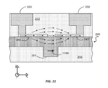
10811 Figure 11 is a simplified schematic diagram illustrating a cross section
of the waveguide
structure shown in Figure 2, where the direction of the induced electric field
is illustrated with
arrows, according to some embodiments. As illustrated, the small arrows show
the induced
electric field direction which generally points along the positive x-direction
through the
electrodes of the device. The electric field curves in a convex manner both
above and below the
electrodes, as illustrated. Furthermore, the large arrow (1150) pointing in
the positive x-direction
illustrates the direction of polarization of an optical mode that may travel
through the slab layer
and the waveguide.
Figures 12-15 - Fabrication Methods for Electro-optical Devices
10821 Recent technology advancements have demonstrated successful growth of
ferroelectric
thin films on planar Si substrates using complex molecular beam epitaxy (MBE)
techniques,
which makes it possible for monolithic integration of various complex oxides
in electro-optical
16
CA 03170572 2022- 9- 2
WO 2021/178332
PCT/US2021/020341
devices using semiconductor processing technologies. BaTiO3 or BTO is
considered the material
of choice for next generation electro-optical switches due to its high Pockels
coefficient, high
band width, and low dielectric loss. In some embodiments, a blanket BTO thin
film may be
epitaxially grown on a silicon substrate using SrTiO3 as a buffer. A silicon
dioxide (SiO2)
bonding layer may he then overlaid on the BTO thin film. On another silicon
wafer, a silicon
waveguide is formed and is surrounded by a silicon dioxide cladding layer
having a flat top
surface, which can be obtained by, for example, chemical. mechanical polishing
after blanket
deposition of the silicon dioxide layer over the silicon waveguide. The first
wafer with the
blanket BTO film formed thereon is bonded to the second wafer through wafer-to-
wafer bonding,
so that the blanket gro fihn is transferred to the flat top surface of the
silicon dioxide cladding
on the second wafer. This first wafer is subsequently removed (e.g., by
grinding and/or chemical
mechanical polishing), and electrodes or contacts are then formed in the BTO
film to allow
application of an electric field across the contacts. This process involves
transferring oldie Erro
film from one substrate to another, and is thus inefficient, costly, and
limiting on the underlying
device architecture. Figures 12-15 illustrate improved methods for the
fabrication process of
various electro-optical device architectures, according to various
embodiments.
10831 Figures 12A-G are schematic diagrams illustrating a fabrication method
for constructing
the electro-optical device with a ridge waveguide positioned opposite to the
electrodes, according
to some embodiments.
10841 Figure 12A illustrates initial steps for constructing a device,
including depositing a seed
layer (1204) on a substrate layer (1202), and depositing an electro-optic
layer (1206) on the seed
layer (1204). The sequential layers may be epitaxially deposited, or they may
be deposited using
another technique. In some embodiments, a first wafer comprising a first layer
stack may be
received, where the first layer stack includes the illustrated substrate layer
(1202), seed layer
(1204), and electro-optic layer (1206). In other words, a pre-fabricated wafer
corresponding to
that illustrated in Figure 12A may be received from a manufacturer.
Alternatively, a partially
completed wafer comprising one or more of the seed layer (1204), substrate
layer (1202), and/or
electro-optic layer (1206) may be received, and the remaining layers may be
deposited to
complete the wafer.
10851 In some embodiments, the substrate layer is a silicon-on-insulator (SOI)
wafer, and the
first portion of the substrate layer is a top silicon layer of the SO1 wafer
in contact with the seed
layer. The SOI wafer may include a semiconductor (e.g., silicon or Si) base,
an oxide layer (e.g.,
silicon dioxide or SiO2) on the semiconductor base substrate, and a
semiconductor layer (e.g.,
silicon) on the oxide layer. Although a silicon-based SOI substrate having a
silicon layer on a
silicon dioxide layer on a silicon base substrate is used herein as an example
of the SOI substrate,
17
CA 03170572 2022- 9- 2
WO 2021/178332
PCT/US2021/020341
the SOI substrate can be based on other types of semiconductors (e.g.,
germanium or gallium
arsenide). The thickness of the silicon layer and the S102 layer on the SOI
substrate can vary
according to various embodiments. In some embodiments, the thickness of the
silicon layer on
the SOI substrate is equal to or less than 150nm, the thickness of the SiO2
layer can range from
0.5 to 4 ilm, and the thickness of the silicon base can range from 100 pm to 2
mm.
10861 In some embodiments, the seed layer is composed of one of strontium
titanate (STO),
barium strontium titanate (BST), hafnium oxide, zirconium oxide, titanium
oxide, graphene
oxide, tantalum oxide, lead zirconium titanate (PZ'F), lead lanthanum
zirconium titanate (PLZT),
strontium barium niobate (SBN), magnesium oxide (MgO), germanium (Cie), or the
like. In some
embodiments, the seed layer may be thinner than 30nm, and may serve as an
interworking layer
to attach the electro-optic layer to the substrate layer. In these
embodiments, the seed layer and
the interworking layer may ultimately be removed in a subsequent fabrication
step. Alternatively,
in some embodiments the seed layer may be thicker (e.g., from 4nm-300nm in
thickness), and
may be subsequently etched to split the seed layer into a first electrode
separated from a second
electrode, as described in greater detail below.
10871 In some embodiments, the electro-optic layer is composed of one of
barium titanate
(BTO), barium strontium titanate (BST), lithium niobite, lead zirconium
titanate (PZT), lead
lanthanum zirconium titanate (purr), aluminum oxide, aluminum nitrite, or
strontium barium
niobate (SBN). In some embodiments, the first cladding layer may be composed
of silicon
dioxide, or another material.
10881 In some embodiments, depositing the seed layer on the substrate layer
includes obtaining
an SOI substrate having a clean silicon surface (e.g., Si [001] 21
reconstructed surface), and
passivating the silicon surface using conventional techniques. After the
silicon surface is
passivated, a SrTiO3 buffer layer can be epitaxially grown on the silicon
layer. A thin film (- 3
run to 30 nm) epita.xially grown SrTiO3 layer may be grown initially as a
buffer layer to promote
the epitaxial growth of the subsequently deposited BaTiO3 layer. In some
embodiments, the first
few MLs (1-3 ML) of SrTiO3 can be grown at a lower temperature (e.g., 100-300
C) under, for
example, an oxygen pressure of 10-8-1.5 x10'Torr, in order to avoid oxidation
at the silicon
surface. These few MIA of SrTiO3 is mostly amorphous so an annealing process
at higher
temperature (e.g., 500-750 C) in ultrahigh vacuum conditions (e.g., pressure
<5 x I0-9Torr)
may be performed to crystallize the SrTiO3 grown on the silicon surface. More
SrTiO3 may be
then grown at higher temperature (e.g., 500-600 C), or at lower temperature
(e.g., 300-500 C)
followed by annealing at higher temperature (e.g., 550-750 C) until a desired
thickness of the
SrTiO3 buffer layer is achieved.
18
CA 03170572 2022- 9- 2
WO 2021/178332
PCT/US2021/020341
10891 Figure 12b illustrates how the electro-optic layer is etched to
construct a ridge waveguide
structure (1224). Subsequent to etching the electro-optic layer, a first
cladding layer (1208) is
deposited on the electro-optic layer (1206). For example, before depositing
the first cladding
layer, a ridge structure may be formed from a uniform electro-optic layer. In
some embodiments,
the ridge waveguide structure can be formed by obtaining an electro-optic
layer with a e.g., 200 --
350 run thickness, masking the area on the electro-optic layer where the ridge
waveguide
structure is to be situated, and etching the electro-optic layer on the SOT
substrate using an
anisotmpic etching (e.g., RIE) process to thin down the unmasked portion of
the electro-optic
layer to, for example, less than 150 nm. The first cladding layer is then
deposited on the ridge
waveguide structure and the portion of the electro-optic layer that has been
thinned down.
10901 Figure 12C illustrates planarizing the first cladding layer (.1210). For
example, the upper
surface of the first cladding layer shown in Figure 12A may not be sufficient
planar, and the first
cladding layer may be planariz.ed to reduce variations in thickness of the
first cladding layer.
10911 Figure 1213 illustrates bonding the planarized first cladding layer
(1210) to a wafer
(1212). In some embodiments, the upper surFace of the first cladding layer may
be bonded to the
wafer. In some embodiments, the wafer (1212) comprises an optical interposer,
or the wafer may
be another type of circuit component of the device. In general, the wafer may
contain any of a
variety of different types of components that are to be configured proximate
to the ridge
waveguide.
10921 Figure 12E illustrates removing the substrate layer (1202) from what is
now shown as the
upper surface of the device. Removing th.e substrate layer m.ay expose the
seed layer.
10931 Figure 12F illustrates etching the seed layer to split the seed layer
into a first electrode
(1214) separated from a second electrode (1216). Etching the seed layer may be
performed to
expose a portion of the electro-optic layer. The method may continue to
deposit a second
cladding layer (1218) on the etched seed layer and the exposed portion of the
electro-optic layer.
10941 Figure 12G illustrates etching the second cladding layer to expose a
first portion of the
first electrode, etching the second cladding layer to expose a second portion
of the second
electrode, depositing a first lead (1220) onto the first electrode (1214)
through the exposed first
portion, and depositing a second lead (1222) onto the second electrode (1216)
through the
exposed second portion. The first and second leads may be composed of a
conductive material
such as a metal (e.g., copper, gold, or the like), or alternatively they may
be composed of a
semiconductor. The final device may be structurally similar to the device
illustrated in Figure 2,
for example.
10951 Figures 13A-E are schematic diagrams illustrating a fabrication method
for constructing
the electro-optical device with a ridge waveguide positioned on the opposite
side as the
19
CA 03170572 2022- 9- 2
WO 2021/178332
PCT/US2021/020341
electrodes with leads penetrating through the slab layer of the waveguide,
according to some
embodiments. The method steps shown in Figures 13A-E may be used to construct
a device
similar to the device shown in Figure 3, for example.
10961 Figure 13A illustrates initial steps for fabricating a device, including
depositing a seed
layer (1304) on a substrate layer (1302), depositing an electro-optic layer
(1306) on the seed
layer (1304), and depositing an electrode layer (1308) on the electro-optic
layer (1306). The
sequential layers may be cpitaxially deposited, or they may be deposited using
another technique.
Alternatively, a completed wafer such as that shown in Figure 13A may be
received from a
manufacturer. Alternatively, a partially completed wafer comprising one or
more of the seed
layer (1304), substrate layer (1302), and/or electro-optic layer (1306) may be
received, and the
remaining layers may be deposited to complete the wafer.
10971 In some embodiments, the seed layer is composed of one of strontium
titanate (STO),
barium strontium titanate (BST), hafnium oxide, zirconium oxide, titanium
oxide, graphene
oxide, tantalum oxide, lead zirconium titanate (PZI.), lead lanthanum
zirconium titan.ate (PLED,
strontium barium niebate (SBN), magnesium oxide (MgO), germanium, or the like.
10981 In some embodiments, the clectro-optic layer is composed of one of
barium titanate
(BTU), barium strontium titanate (BST), lithium niobite, lead zirconium
titanate (PEI), lead
lanthanum zirconium titanate (PLZT), aluminum oxide, aluminum nitrite, or
strontium barium
niobate (SBN).
10991 Figure 13B illustrates etching the electrode layer (1308) to expose a
portion of the
electro-optic layer and split th.e electrode layer into a first electrode
(1.310) separated from a
second electrode (1312). Subsequent to performing the etching, a first
cladding layer (1314) is
deposited on the exposed portion of the electro-optic layer and the first and
second electrodes.
101001 Figure 13C illustrates planarizing the first cladding layer and bonding
the planarized first
cladding layer (1314) to a wafer (1316). For example, th.c first cladding
layer may be planarized
to increase its thickness uniformity and to improve bonding to the wafer. The
device may be
flipped upside down prior to bonding to the wafer, such that the planarized
first cladding layer is
now on the bottom of the device for bonding to the wafer. In some embodiments,
the wafer
(1316) comprises an optical interposer, or the wafer may be another type of
circuit component of
the device. In general, the wafer may contain any of a variety of different
types of components
that are to be configured proximate to the electrodes.
101.011 Figure 13D illustrates removing the substrate layer (1302) and the
seed layer (1304), and
after removing the substrate layer and the seed layer, etching the electro-
optic layer (1306) to
produce a ridge waveguide (1318) with a first thickness (1326) disposed
between first (1320) and
second (1322) slab layers with a second thickness (1328) smaller than the
first thickness (1326).
CA 03170572 2022- 9- 2
WO 2021/178332
PCT/US2021/020341
In some embodiments, to further improve the electro-optic coefficient in the
region near the ridge
waveguide, not just the substrate layer (1302) and the seed layer (1304) are
removed but a
portion of the elcctro-optic layer 1306 is also removed to remove any c-axis
clectro-optic
material that was grown in the region close to the seed layer (e.g., in the
case of an STO seed and
BTO electro-optic layer). After etching the ridge waveguide, a second cladding
layer (1324) may
be deposited on the first and second slab layers and the ridge waveguide
structure.
101021 Figure 13E illustrates etching through the second cladding layer (1324)
and the first slab
layer to expose a first portion of the first electrode, etching through the
second cladding layer and
the second slab layer to expose a second portion of the second electrode,
depositing a first lead
(1330) onto the first electrode (1310) through the exposed first portion, and
depositing a second
lead (1332) onto the second electrode (1312) through the exposed second
portion. The first and
second leads may be composed of a conductive material such as a metal, or
alternatively they
may be composed ola semiconductor.
101031 Figures 14A-E are schematic diagrams illustrating a fabrication method
for constructing
the electro-optical device with a ridge waveguide positioned on the same side
as the electrodes,
according to some embodiments. The method steps shown in Figures 14A-E may be
used to
construct a device similar to the device shown in Figure 4, for example.
101041 Figure 14A illustrates initial steps for fabricating a device,
including depositing a seed
layer (1404) on a substrate layer (1402), depositing an electro-optic layer
(1406) on the seed
layer (1404), and depositing a first cladding layer (1408) on the electro-
optic layer (1406). The
sequential layers may be epitaxially deposited, or they may be deposited using
another technique.
Alternatively, a completed wafer such as that shown in Figure 14A may be
received from a
manufacturer. Alternatively, a partially completed wafer comprising one or
more of the seed
layer (1404), substrate layer (1402), electro-optic layer (1406), and/or first
cladding layer (1408)
may be received, and the remaining layers may be deposited to complete the
wafer.
101051 In some embodiments, the electro-optic layer is composed of one of
barium titanate
(BTO), barium strontium titanate (BST), lithium niobite, lead zirconium
titanate (PZT), lead
lanthanum zirconium titanate (PLZT), aluminum oxide, aluminum nitrite, or
strontium barium
niobate (SBN).
101061 Figure 14B illustrates planarizing the first cladding layer (1408) to
increase thickness
unifortnity of the first cladding layer, and bonding the planarized first
cladding layer (1408) to a
wafer (1410). 'The device may be flipped upside down prior to bonding to the
wafer, such that the
plariarized first cladding layer is now on the bottom of the device for
bonding to the wafer. In
some embodiments, the wafer (1410) comprises an optical interposer, or the
wafer may be
21
CA 03170572 2022- 9- 2
WO 2021/178332
PCT/US2021/020341
another type of circuit component of the device. In general, the wafer may
contain any of a
variety of different types of components that are to be configured proximate
to the seed layer.
101.071 Figure I 4C illustrates removing the substrate layer (1402) and the
seed layer (1404), and
after removing the substrate layer and the seed layer, etching the electro-
optic layer to produce a
ridge waveguide (1412) with a first thickness (1418) disposed between a first
slab layer (1414)
and a second slab layer (1416), wherein the first and second slab layers have
a second thickness
(1420) smaller than the first thickness (1418). In some embodiments, to
further improve the
electro-optic coefficient in the region near the ridge waveguide, not just the
substrate layer
(1402) and the seed layer (1404) are removed but a portion of the electro-
optic layer 1406 is also
removed to remove any c-axis electro-optic material that was grown in the
region close to the
seed layer (e.g., in the case of an STO seed and BTO electro-optic layer).
101081 Figure 14D illustrates depositing a first (1422) and second (1424)
electrode on the left
and right sides, respectively, or the ridge waveguide structure (1412), and
depositing a second
cladding layer (1426) on the first and second electrodes and the ridge
waveguide structure. In
some embodiments, the first and second electrodes are composed of one of
strontium titanate
(STO), barium strontium titanate (BST), hafnium oxide, zirconium oxide,
titanium oxide,
graphene oxide, tantalum oxide, lead zirconium titanate (PZT), lead lanthanum
zirconium titanate
(PLZT), or strontium barium niobate (SBN).
101091 Figure 14E illustrates etching through the second cladding layer to
expose a first portion
of the first electrode, etching through the second cladding layer to expose a
second portion of the
second electrode, depositing a first lead (1428) onto the first electrode
(1422) through the
exposed first portion, and depositing a second lead (1430) onto the second
electrode (1424)
through the exposed second portion. The first and second leads may be composed
of a conductive
material such as a metal, or alternatively they may be composed of a
semiconductor.
101101 Figure 15A-E illustrate methods for fabricating a photonic device
exhibiting a sandwich
architecture, according to some embodiments. The method steps shown in Figures
15A-E may be
used to construct a device similar to the device shown in Figure 5, for
example.
101111 Figure 15A illustrates a cross section of a first wafer (1500)
comprising an electrode layer
(1504) disposed on a first substrate layer (1506) and an electro-optic layer
(1502) disposed on the
electrode layer (1504). Alternatively, in some embodiments the electro-optic
layer (1502) is
disposed on a seed layer (not shown). The first wafer may be prefabricated by
a wafer
manufacturer and received for further fabrication steps as described in
Figures 15C-E, in some
embodiments. Alternatively, the first wafer may be fabricated in-house. For
example, the
electrode layer and the electro-optic layer may be sequentially deposited on
the first substrate
22
CA 03170572 2022- 9- 2
WO 2021/178332
PCT/US2021/020341
layer, by utilizing epitaxial deposition or any of a variety of other
deposition techniques, as
variously described throughout this disclosure.
101.121 Figure 158 illustrates a cross section of a second wafer (1501)
comprising a second
substrate layer (1.512) disposed underneath a second cladding layer (1510) and
a second strip
waveguide structure (1508) disposed within the second cladding layer and near
the upper surface
of the second cladding layer. The second wafer (1501) may be prefabricated by
a wafer
manufacturer and received for further fabrication steps as described in
Figures 15C-E, in some
embodiments. Alternatively, the second wafer may be fabricated in-house, as
desired.
101131 In some embodiments, the first wafer (1500) is flipped over, and the
exposed surface of
the electro-optic layer (1502) of the first wafer is bonded to exposed surface
of the second
cladding layer (1510) of the second wafer. Accordingly, the first and second
wafers are bonded
together.
101141 Figure 15C illustrates how, in some embodiments, after bonding the
first wafer to the
second wafer, the first cladding layer (1506) is removed, and the electrode
layer (1504) is etched
to split the electrode layer into a first electrode (1514) separated from a
second electrode (1516).
In other embodiments, the electrode layer (1504) serves as a relatively thin
seed layer that is
ultimately removed. To further improve the electro-optic coefficient in the
region near the
surface of the seed layer, a portion of the electro-optic layer (1502) may be
removed in addition
to the substrate layer (1506) and the electrode/seed layer (1504). In these
embodiments, after this
removal of the seed layer, Of any partial removal step, a new electrode layer
may be deposited
and etched as described above.
101151 Figure 15D illustrates bow a first strip waveguide structure (1520) is
deposited between
the first (1514) and second (1516) electrodes. In some embodiments, the
deposition process is
followed by a planarization step to remove excess material from the region
above the electrodes,
e.g., by way of lithographic patterning or chemical mechanical polishing
(CMP). In some
embodiments, the material used for the strip waveguide structures (1520)
and/or (1508) is as
described above in reference to FIG. 5, and may be, e.g., silicon nitride.
Subsequently, a first
cladding layer (1518) is deposited on the first and second electrodes and the
first strip waveguide
structure.
101161 Finally, Figure 15E illustrates how the first cladding layer (1518) is
etched to expose a
portion of the first electrode (1514) and a portion of the second electrode
(1516). A first lead
(1522) is then deposited on the exposed portion of the first electrode, and a
second lead (1524) is
deposited on an exposed portion of the second electrode. Figure 15E
illustrates an embodiment
where the lead is deposited on the upper surface of the first and second
electrodes. However, in
other embodiments, the exposed portions of the first and second electrodes may
themselves be
23
CA 03170572 2022- 9- 2
WO 2021/178332
PCT/US2021/020341
etched, such that the first and second leads are deposited within some
distance within the cross
section of the first and second electrodes, or potentially on the upper
surface of the electro-optic
layer (1502).
101171 Figure 16 illustrates a cross section of a first wafer including a
layer stack that may be
received as part of a fabrication process for various devices described
herein, according to
various embodiments. As illustrated, a first insulating substrate layer (1502)
may be (optionally)
disposed beneath a seed layer (1504), which is disposed beneath an clectro-
optic layer (1506),
which is (optionally) disposed beneath an electrode layer (1508), which is
(optionally) disposed
beneath a second insulating substrate layer (1510). It is noted that the first
wafer may be of
various types depending on the specific fabrication method to be employed, as
the seed layer,
electrode layer, and second substrate layer may be optionally present or not
present, as desired.
10118] In some embodiments, the seed layer (1504) may be subsequently etched
to form a first
electrode separated from a second electrode. Alternatively, in some
embodiments the seed layer
simply serves to provide an intcrworking layer between the clectro-optic layer
and the first
substrate layer, and the seed layer is ultimately removed during the
fabrication process. In these
embodiments, the electrode layer (1508) may be etched to form the first and
second electrodes.
101191 The terminology used in the description of the various described
embodiments herein is
for the purpose of describing particular embodiments only and is not intended
to be limiting. As
used in the description of the various described embodiments and the appended
claims, the
singular forms "a", "an" and "the" are intended to include the plural font's
as well, unless the
context clearly indicates otherwise. It will also be understood that the term.
"and/or" as used
herein refers to and encompasses any and all possible combinations of one or
more of the
associated listed items. It will be further understood that the terms
"includes," "including,"
"comprises," and/or "comprising," when used in this specification, specify the
presence of stated
features, integers, steps, operations, elements, and/or components, but do not
preclude the
presence or addition of one or more other features, integers, steps;
operations, elements,
components, and/or groups thereof
101201 As used herein, the term "if' is, optionally, construed to mean "when"
or "upon" or "in.
response to determining" or "in response to detecting" or "in accordance with
a determination
that," depending on the context.
10121.1 The foregoing description, for purpose of explanation, has been
described with reference
to specific embodiments. However, the illustrative discussions above are not
intended to be
exhaustive or to limit the scope of the claims to the precise forms disclosed.
Many modifications
and variations are possible in view of the above teachings. The embodiments
were chosen in
order to best explain the principles underlying the claims and their practical
applications, to
24
CA 03170572 2022- 9- 2
WO 2021/178332
PCT/US2021/020341
thereby enable others skilled in the art to best use the embodiments with
various modifications as
are suited to the particular uses contemplated.
101221 It is also understood that the examples and embodiments described
herein arc for
illustrative purposes only and that various modifications or changes in light
thereof will be
suggested to persons skilled in the art and are to be included within the
spirit and purview of this
application and scope of the appended claims.
CA 03170572 2022- 9-2