Note: Descriptions are shown in the official language in which they were submitted.
WO 2021/211954
PCT/US2021/027662
OPTICALLY TRANSPARENT 3D PRINTED
POLYSILOXANE SCINTILLATORS
[mon This invention was made with Government support under
Contract No.
DE-AC52-07NA27344 awarded by the United States Department of Energy. The
Government has certain rights in the invention.
FIELD OF THE INVENTION
[0002] The present invention relates to radiation detection,
and more particularly to
polysiloxane-based inks for polysiloxane scintillators capable of detecting
ionizing
radiation, and methods of making and using the same.
BACKGROUND
[0003] Scintillation detectors serve as the backbone of
radiation detection. Although
some of the most cost efficient and most expensive radiation detectors use
different
technologies, the in aj ority of applied radiation detectors rely on
scintillation to measure
radiation energy at reasonable cost and robustness. Basic scintillation
detectors identify
when radiation has deposited energy inside the scintillator and how much
energy was
deposited. These detectors allow users to detect the presence and spectrum of
radiation.
The spectrum can be used to identify the radiation source, including
distinguishing threat
from non-threat sources. However, this source identification is limited by the
energy
resolution of the detector, the presence of shielding around the source,
radioactive
backgrounds, and short measurement durations or long distances, which each
reduce the
- 1 -
CA 03171132 2022- 9-8
WO 2021/211954
PCT/US2021/027662
statistical precision of the measurement. Advanced detectors augment this
basic design by
adding capabilities that detect more parameters about the radiation and its
source.
[0004] To enhance DNN (U.S. Office of Defense Nuclear
Nonproliferation)
applications, more advanced detectors distinguish neutrons from gamma-rays, as
neutrons
are an indicator of SNM (special nuclear material) sources. One approach to
this is pulse-
shape discrimination (PSD), a technique in which the scintillating material is
doped with
fluors that produce a distinct pulse shape when hit with fast neutrons. Solid
PSD plastic
scintillators are a topic of active research and have seen significant
improvements in their
scale, light output, and discrimination ability in recent years. However, they
arc still
limited in scale and elements larger than about 20 cm are difficult to
produce. Liquid PSD
scintillators are more available, but liquid-based detectors are less robust
and less portable
than solid detectors. PSD detectors of either type also utilize expensive fast
electronic
instrumentation that further raises their cost.
[0005] Another approach to neutron identification involves
doping the scintillating
material with a substance such as gadolinium or lithium-6 that produces
additional
radiation when it captures a thermal neutron. This approach is similar to that
of the now-
standard helium-3 detectors, but doped scintillators have not yet exhibited
neutron-
gamma separation competitive with helium-3. Thus, identification of neutron
radiation
for SNM detection currently is limited to the choice between small and
expensive solid
PSD detectors, less robust and still expensive liquid PSD detectors, or
neutron capture
detectors with limited efficiency.
[0006] Other advanced scintillation detectors allow the user
to identify the location of
radiation interactions. These detectors typically employ multiple, separately-
instrumented
detector volumes. The location of the radiation interaction can be determined
by
observing the detector volume having the radiation interaction. Unfortunately,
the ability
- 2 -
CA 03171132 2022- 9-8
WO 2021/211954
PCT/US2021/027662
to identify the precise location of the interactions is limited by the size of
a single
scintillator volume: using smaller volumes enables more precise location-
finding, but
increases the total number of volumes, thereby increasing the cost of
instrumenting each
volume separately. The number of volumes and associated cost also rises if the
detector is
subdivided along more dimensions, making 3D position-finding particularly
difficult and
expensive.
[0007] Some detectors are able to locate an interaction
within a single volume using a
double-ended instrumentation. However, this capability requires costly fast
electronics
and only works in a single dimension. Thus, a detector that can precisely
locate radiation
interactions without using many separately instrumented volumes-particularly
if such a
detector could do so along multiple dimensions and without fast electronics-
will vastly
improve both the accuracy and cost-benefit of detection activities.
[0008] What is needed, and absent from the art, is
development of an optically
transparent scintillator capable of having fine and/or periodic features
comprised of
multiple materials for enhanced scintillator capability, such as directional
sensing of
radiation.
- 3 -
CA 03171132 2022- 9-8
WO 2021/211954
PCT/US2021/027662
SUMMARY
[0009] In one aspect, an ink for forming a scintillator
product includes a
phenylated siloxane polymer having at least one functional group per molecule
for
crosslinking, a filler having a refractive index about matching a refractive
index of the
phenylated siloxane polymer, where the refractive indices are within about 5 %
of one
another, a rheology modifier, and at least one fluorescent dye.
[0010] In another aspect, a scintillator product includes a
three-dimensional (3D)
structure having physical characteristics of formation by additive
manufacturing,
where the structure includes a material comprising a phenylated siloxane
polymer, a
filler having a refractive index about matching a refractive index of the
phenylated
siloxanc polymer, where the refractive indices are within about 5 % of one
another,
and at least one fluorescent dye. In addition, the scintillator product is
optically
transparent.
[0011] In yet another aspect, a method of forming an
optically transparent
scintillator product includes extruding an ink for forming a three-dimensional
(3D)
structure using an additive manufacturing technique and curing the 3D
structure for
forming the optically transparent scintillator product. The ink is a
scintillator material
including a phenylated siloxane polymer having at least one functional group
per
molecule for crosslinking, a filler having a refractive index about matching a
refractive index of the phenylated siloxane polymer, where the refractive
indices are
within about 5% of one another, and at least one fluorescent dye.
[0012] Other aspects and advantages of the present invention
will become apparent
from the following detailed description, which, when taken in conjunction with
the
drawings, illustrate by way of example the principles of the invention.
- 4 -
CA 03171132 2022- 9-8
WO 2021/211954
PCT/US2021/027662
BRIEF DESCRIPTION OF THE DRAWINGS
[0013] For a fuller understanding of the nature and
advantages of the present
invention, as well as the preferred mode of use, reference should be made to
the following
detailed description read in conjunction with the accompanying drawings.
[0014] FIG. 1A is a schematic diagram of a high level
perspective illustration of a
scintillator system.
[0015] FIG. 1B is a plan top view of the scintillator of FIG.
14 illustrating how
gamma radiation passes through and deposits energy in four of the cubes of the
scintillator structure.
[0016] FIG. 2 is a perspective view of a system illustrating
a MMSS scintillator
structurc adapted for usc in a scatter camera application.
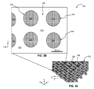
[0017] FIG. 3A is schematic drawing of a 3D printed log-pile
structure of a
polysiloxane scintillator, according to one inventive aspect.
[0018] FIG. 3B is a magnified side view of a portion the 3D
printed log-pile structure
of FIG. 34 as a heterogeneous polysiloxane scintillator, according to one
approach.
[0019] FIG. 4 is schematic drawing of a 3D-printed structure
having a compositional
gradient of scintillator material, according to one inventive aspect.
[0020] FIG. 5 is a schematic drawing of a simplified layout
of an instrument system,
according to one inventive aspect.
[0021] FIG. 6 is a flow chart of a method, according to one
inventive aspect.
[0022] FIG. 7 is an image of 3D printed, structured, blue-
emitting polysiloxane
scintillator lattice, according to one inventive aspect.
[0023] FIG. 8A is an image of an optically transparent 3D
printed monolithic
polysiloxane scintillator, according to one inventive aspect.
- 5 -
CA 03171132 2022- 9-8
WO 2021/211954
PCT/US2021/027662
[0024] FIG. 8B depicts images of different views of an
optically transparent 3D
printed lattice polysiloxanc scintillator, according to one inventive aspect;
part (a) is a
perspective view of the scintillator, .part (b) is a top down view of the
scintillator, and
part (c) is a side view of the scintillator.
[0025] FIG. 9A is an image of a 3D structured heterogenous
polysiloxane scintillator,
according to one inventive aspect.
[0026] FIG. 9B is an image of a 3D structured heterogeneous
polysiloxane scintillator
having the second scintillator material fully infilled between the filaments
of the first
scintillator material, according to one inventive aspect.
[0027] FIG. 10A is an image of monolithic 3D printable
polysiloxane scintillators
under UV excitement having different emission colors and intensities,
according to one
aspect of an invention.
[0028] FIG. 10B is an image of a monolithic 3D printable
polysiloxane scintillator
under UV excitement having a 525 nm emission color, according to one inventive
aspect.
[0029] FIG. 11 is a plot of photoluminescence spectra of
various 3D printable
polysiloxane scintillators, according to one inventive aspect.
- 6 -
CA 03171132 2022- 9-8
WO 2021/211954
PCT/US2021/027662
DETAILED DESCRIPTION
[0030] The following description is made for the purpose of
illustrating the general
principles of the present invention and is not meant to limit the inventive
concepts
claimed herein. Further, particular features described herein can be used in
combination
with other described features in each of the various possible combinations and
permutations.
[0031] Unless otherwise specifically defined herein, all
terms are to be given their
broadest possible interpretation including meanings implied from the
specification as well
as meanings understood by those skilled in the art and/or as defined in
dictionaries,
treatises, etc.
[0032] It must also be noted that, as used in the
specification and the appended
claims, the singular forms "a," "an" and "the" include plural referents unless
otherwise
specified.
[0033] Further, as used herein, all percentage values are to
be understood as
percentage by weight (wt. %), unless otherwise noted. Moreover, all
percentages by
weight are to be understood as disclosed in an amount relative to the bulk
weight of an
organic plastic scintillator material, in various approaches.
[0034] Unless expressly defined otherwise herein, each
component listed in a
particular approach may be present in an effective amount. An effective amount
of a
component means that enough of the component is present to result in a
discernable
change in a target characteristic of the ink, printed structure, and/or final
product in which
the component is present, and preferably results in a change of the
characteristic to within
a desired range. One skilled in the art, now armed with the teachings herein,
would be
able to readily determine an effective amount of a particular component
without having to
resort to undue experimentation.
- 7 -
CA 03171132 2022- 9-8
WO 2021/211954
PCT/US2021/027662
[0035] The present disclosure includes several descriptions
of exemplary "inks" used
in an additive manufacturing process to form the inventive optics described
herein. It
should be understood that "inks" (and singular forms thereof) may be used
interchangeably and refer to a composition of matter comprising a plurality of
particles
coated with/dispersed throughout a liquid phase such that the composition of
matter may
be -written," extruded, printed, or otherwise deposited to form a layer that
substantially
retains its as-deposited geometry and shape without excessive sagging,
slumping, or other
deformation, even when deposited onto other layers of ink, and/or when other
layers of
ink are deposited onto the layer. As such, skilled artisans will understand
the presently
described inks to exhibit appropriate rheological properties to allow the
formation of
monoliths and/or fine structures via deposition of multiple layers of the ink
(or in some
cases multiple inks with different compositions) in sequence.
[0036] The following description discloses several preferred
structures formed via
direct ink writing (DIW), extrusion freeform fabrication, or other equivalent
techniques
(collectively referred to as DIW herein) and therefore exhibit unique
structural and
compositional characteristics conveyed via the precise control allowed by such
techniques. The physical characteristics a structure formed by DIW may include
having
lower layers of the structure are slightly flattened, slightly disfigured from
original
extrusion (e.g., see slight droop of the filament in FIG. 9A), etc. by weight
of upper layers
of structure, due to gravity, etc. The three-dimensional structure formed by
DIW may
have a single continuous filament that makes up at least two layers of the 3D
structure.
[0037] As al so used herein, the term "about" when combined
with a value refers to
plus and minus 10% of the reference value. For example, a length of about 10
nm refers
to a length of 10 mu 1 nm, a temperature of about 50 C refers to a
temperature of 50 C
C, etc.
- 8 -
CA 03171132 2022- 9-8
WO 2021/211954
PCT/US2021/027662
[0038] As additionally used herein, a material that is
"optically transparent" refers to
a material that is substantially free of optical grain boundaries or light
scatter defects,
such that the material is capable of transmitting at least about 90% of
incident light. In
one approach, optical transparency may be measured as the material having
scattering of
light less than about 5 % per cm.
[0039] The description herein is presented to enable any
person skilled in the art to
make and use the invention and is provided in the context of particular
applications of the
invention and their requirements. Various modifications to the disclosed
approaches to
inventive aspects will be readily apparent to those skilled in the art upon
reading the
present disclosure, including combining features from various approaches to
create
additional and/or alternative approaches thereof.
[0040] Moreover, the general principles defined herein may be
applied to other
approaches and applications without departing from the spirit and scope of the
present
invention. Thus, the present invention is not intended to be limited to the
approaches
shown but is to be accorded the widest scope consistent with the principles
and features
disclosed herein.
[0041] The following description discloses several preferred
inventive aspects of
ink formulations for forming optically transparent 3D printed polysiloxane
scintillator
material and/or related systems and methods.
[0042] In one general aspect, an ink for forming a
scintillator product includes a
phenylated siloxane polymer having at least one functional group per molecule
for
crosslinking, a filler having a refractive index about matching a refractive
index of the
phenylated siloxane polymer, where the refractive indices are within about 5 %
of one
another, a rheology modifier, and at least one fluorescent dye.
- 9 -
CA 03171132 2022- 9-8
WO 2021/211954
PCT/US2021/027662
[0043] In another general aspect, a scintillator product
includes a three-
dimensional (3D) structure having physical characteristics of formation by
additive
manufacturing, where the structure includes a material comprising a phenylatcd
siloxane polymer, a filler having a refractive index about matching a
refractive index
of the phenylated siloxane polymer, where the refractive indices are within
about 5 %
of one another, and at least one fluorescent dye. In addition, the
scintillator product is
optically transparent.
[0044] In yet another general aspect, a method of forming an
optically transparent
scintillator product includes extruding an ink for forming a three-dimensional
(3D)
structure using an additive manufacturing technique and curing the 3D
structure for
forming the optically transparent scintillator product. The ink is a
scintillator material
including a phenylated siloxane polymer having at least one functional group
per
molecule for crosslinking, a filler having a refractive index about matching a
refractive index of the phenylated siloxane polymer, where the refractive
indices are
within about 5% of one another, and at least one fluorescent dye.
[0045] A list of acronyms used in the description is provided
below.
3D Three-dimensional
3HF 3-hydroxyflavone
APID anisotropic particle identification
Bis-MSB 1,4-bis(2-methylstyryl)benzene
Celsius
Cs cesium
DIW direct-ink writing
DLP Digital light processing
DPA 9,10-diphenylanthracene
- 10 -
CA 03171132 2022- 9-8
WO 2021/211954
PCT/US2021/027662
kg kilogram
micron
meter
mm millimeter
MDAC 7- cliethylamino-4-rnethylcoumarin
MeV mega electron volts
m-TP m-terphenyl
nm nanometer
a-NPO a-naphthylphenyloxazole
PID MMSS Particle-identifying mixed material scintillator
structures
PiPS pillars of plastic scintillators
PL photoluminescence
PPm parts per million
PPO 2,5 -diphenyloxazole
PR position resolving
PSD Pulse Shape Discrimination
PVT poly(vinyltoluene)
SLA stereolithography apparatus
SNM Special nuclear materials
TPB 1,1,4,4-tetraphenylbutadiene
TMQ 2" ,3,3' ,3' "-tetramethyl-p-quaterpheryl
UV ultraviolet
wt.% weight percent
- 11 -
CA 03171132 2022- 9-8
WO 2021/211954
PCT/US2021/027662
[0046] In response to the limitations of conventional
scintillator systems, optical
lattices have emerged as a tool for locating interactions in three dimensions
within a
scintillation detector with reduced instrumentation. One type of detector uses
an
arrangement of scintillating cubes having thin gap separations. Light produced
in one
cube undergoes total internal reflection at the interface between the plastic
and the air
within the gap, thereby resulting in the light preferentially traveling to
cubes in the same
X, Y and Z rows as the origin cube. The optical lattice identifies which
volume the
interaction was in by instrumenting each row in three dimensions, and thus
obviating the
need to instrument each individual cube. For example, a 10 x 10 x 10 optical
lattice
would need 30 instruments instead of 1000. However, current optical lattices
rely on
careful hand assembly, which limits the scale of these detectors and
significantly
compounds the expense. This technological innovation may benefit from a
practical and
cost-effective technique to produce optical lattices with smaller cubes in
greater numbers
than has previously been achieved.
[0047] Moreover, recent advances in material and construction
of scintillator
structures tend to interfere with optimal collection of the light produced in
the scintillator,
thereby reducing the energy resolution of these detectors. The amount of light
initially
emitted is a property of the chemistry of the scintillating material, but the
detector
construction and design play a major role in determining how much of the light
emitted is
collected onto sensors instead of leaked or lost to absorption in the detector
materials. The
increased amount of light observed the better the statistical precision of the
measurement
of the radiation energy. in general, optimizing the light collected, that is,
the precision of
the energy measurement, competes with integrating advanced scintillation-
detection
features. By easing this tradeoff, innovations that improve the ability to
collect light
indirectly enable other advanced capabilities.
- 12 -
CA 03171132 2022- 9-8
WO 2021/211954
PCT/US2021/027662
[0048] The existing advanced scintillating materials owe
their success to substantial
effort to master the complex chemistry behind conventional methods of
scintillator
production. Whether producing a plastic, ceramic, or crystal scintillator,
tight control of
the chemistry is critical to prevent spoilage of the material during its
production. The
challenge increases for larger pieces of scintillating material. For example,
plastic
scintillators are typically produced by bulk polymerization, which is an
exothermic
process. As the piece size grows larger, the surface area to volume ratio
makes dissipating
the heat of polymerization more difficult. As the process complexity grows
with the piece
size, production yields drop, making large pieces particularly expensive.
Conventional
methods such as casting or crystal growth also are limited in their ability to
produce
complex form factors directly, and so instead typically produce solid blocks
that must be
machined to the desired shape. The additional machining critical in these
conventional
methods represents an additional manufacturing operation which further adds to
the
production costs.
[0049] Conventional solid organic scintillators such as
plastics and crystals possess
significant quantities of hydrogen in their composition, making them amenable
for fast
neutron detection via proton recoil reactions. These materials are typically
produced as
monoliths by bulk polymerization or crystal growth methods. However, standard
plastic
scintillators typically include stringent prolonged curing methods, for
example, curing
over several weeks in a strictly inert atmosphere. Single crystals of even
moderately (> 1
cm) sized scintillators typically need to be cured for several days, even at
aggressive
growth rates.
[0050] Recent research has shown bulk structures of various
polysiloxanes is a
scintillator material capable of pulse shape discrimination at dye loading
amounts lower
than that used in typical PVT-based scintillators. However, they typically
suffer from
- 13 -
CA 03171132 2022- 9-8
WO 2021/211954
PCT/US2021/027662
poor mechanical properties and are subject to defects such as bubbling,
cracking, and
other defects. Moreover, additive manufacturing of polysiloxanc technology is
developing as an area of interest for scintillator fabrication.
Stereolithography (SLA),
sometimes known as digital light processing (DLP), is a common technique for
producing
acrylic-based plastics but has not successfully been deployed using
polysiloxanes due to
the difficulty in adapting traditional platinum-based curing chemistries to UV-
curing
processes. In addition, various photoinhibitors used for dimensional control
in SLA
absorb in similar regions as scintillation dyes, thus interfering with the
scintillation
process.
[0051] Various aspects described herein include the
preparation and fabrication of
optically transparent polysiloxane-based scintillators capable of having fine
and/or
periodic features. Methods described herein use extrusion-based additive
manufacturing techniques, e.g., direct ink writing (DIW), for forming
structures
having physical characteristics of 3D printing, e.g., fine features in a
micron scale,
uniform features, periodic features, etc. In preferred approaches, an
optically
transparent polysiloxane-based multimaterial scintillator having fine,
periodic features
is not only capable of detecting ionizing radiation, but also may be capable
of
directional sensing, pulse shape discrimination, etc. In some approaches,
ionizing
radiation refers to gamma rays, beta particles, alpha particles, neutrons,
etc. The
polysiloxane-based scintillators are preferably designed not to detect
infrared light,
radiowaves, magnetic fields, etc.
[0052] Direct ink writing a scintillating ink, as described
herein, allows
fabrication of an extruded scintillator in its final shape onto a substrate
without limit
to size. Moreover, the scintillating ink allows a wide variety of siloxane
chemistry.
Direct-ink-writing affords the possibility of creating fine physical features
(< 1 mm)
- 14 -
CA 03171132 2022- 9-8
WO 2021/211954
PCT/US2021/027662
with single and multicomponent features not attainable by standard polymer
casting
methods. For example, a primary advantage of DIW over conventional organic
scintillator fabrication techniques is the ability to produce fine structural
features from
either single (homogeneous) or multiple (heterogeneous) scintillator
feedstocks within
a single active volume. Structured, heterogenous features allow scintillators
to encode
information about incident radiation that conventional scintillators cannot,
thereby
enhancing detection capabilities beyond what was heretofore attainable.
[0053] As an alternative approach to Pulse Shape
Discrimination (PSD) for
detection of ionizing radiation, various inventive aspects described herein
may be
useful in applications that use a geometry approach for detecting ionizing
radiation.
The methodology of particle-identifying mixed material scintillator structures
(PID
MMSS) includes very fine resolution features of the scintillator geometry are
desirable for encoding information about the incoming radiation.
[0054] FIGS. 1A-1B illustrate an example of a system using
PID MMSS. As
shown, a mixed material scintillator system 100, hereafter MMSS 100, may
include a
plurality of like-sized cubes 102a, 102b formed immediately adjacent one
another,
which cooperatively form a scintillating structure 104. The cubes 102a, 102b
may be
made from two different scintillating materials. The dimensions of the cubes
may
vary to meet the needs of a specific applciation. In one example as shown in
FIG. 1B,
cubes 102a, 102b may have dimensions of 1 mm3. In addition, the configuration
of
the cubes may vary. As shown in FIG. 1A, the cubes 102a, 102b may be arranged
in a
uniform, alternating fashion. The overall shape of the scintillator system may
he
constructed to meet the needs of a specific application. In preferred systems,
an
overall shape of the scintillator system is rectangular, square, etc.
- 15 -
CA 03171132 2022- 9-8
WO 2021/211954
PCT/US2021/027662
[0055] Each of the one type of cubes 102a may be comprised of
scintillating
material that produces a first color of light in response to received
radiation 106
passing therethrough, while each of the other type of cube 102b produce a
second
different color of light in response to radiation 106 passing therethrough.
For
example, the one type of cube 102a may include material that produces green
light,
and the other type of cube 102b may include material that produces blue light.
These
materials and colors are by way of example only and are not meant to be
limiting in
any way; material producing other colors of light may be used. The use of two
dissimilar materials for the cubes 102a, 102b enables the scintillator
structure 104 to
provide output signals that distinguish between gamma and neutron radiation
being
received. In some approaches, the dissimilar material for the cubes 102a, 102b
enables the scintillator structure 104 to provide signals for location of the
path of
radiation 106 being received within the structure 104.
[0056] For example, a neutron produces a short ionizing
tracks in the detector
(e.g., 20 microns from a 1 MeV neutron recoil), and may remain entirely within
one
cube 102a or 102b. Alternatively, when a gamma ray hits one of the cubes 102a,
102b, the gamma ray will produce a recoil electron that deposits energy over a
track
106a spanning several adjacent cubes 102a, 102b, as shown in FIG. 1B that
shows a
plan view of the scintillator structure 104 of FIG. 1A. The radiation 106 of
the gamma
ray produces a scintillating signal from the energy deposited along the track
106a as a
mixture of the two light colors of the two different cubes 102a, 102b. Thus,
the
particle type may he identified by determining if the scintillation signal
from the
irradiation 106 of the scintillator structure 104 has produced light of only
one color
(e.g., indicating a neutron hitting a single cube 102a, 102b) or light having
- 16 -
CA 03171132 2022- 9-8
WO 2021/211954
PCT/US2021/027662
components of both colors (e.g., indicating a gamma's track 106a hitting
multiple
cubes 102a and 102b).
[0057] In various approachcs, analysis of the signal produced
by the scintillator
structure 104 may include incorporating two light sensors 108a, 108b as part
of the
system 100. A light sensor 108a may include a green light sensitive
photomultiplier
tube, and a second light sensor 108b may include a blue light sensitive
photomultiplier tube. The sensors 108a, 108b may be positioned proximate,
adjacent,
etc. the surface 110 of the scintillator structure 104. In more approaches,
the sensors
include light sensors used in conventional scintillators as would be
understood by one
skilled in the art.
[0058] In one example as illustrated in FIG. 1A, the light
sensors 108a, 108b
generate electrical output signals at their outputs 108at, 108131 which are
input to a
detection electronics subsystem 110. The detection electronics substation 110
may be
an integral portion of the system 100 (e.g., housed in a housing which also
includes
the scintillator structure 104), may be fully independent subsystem which is
coupled
via suitable electrical connections to the light sensors 108a, 108b to receive
the
outputs 108at, 108b1, etc. The detection electronics system 110 may optionally
include a controller 110a, as well as suitable memory (e.g., RAM or ROMO, not
shown), as well as an optional display system (e.g., LCD, CRT, LED indicators,
etc.,
not shown). The detection electronics subsystem 110 interprets the signals
from the
light sensors 108a, 108b to determine whether neutrons or gamma radiation is
being
received by the system 100 and provides information to a user to indicate the
type of
radiation, if any, has been detected by the scintillator structure 104.
Accordingly, a
central function of the detection electronics subsystem 110 is to turn the
received
signal into a digital record in memory. This "digitalization" can happen
"fast"
- 17 -
CA 03171132 2022- 9-8
WO 2021/211954
PCT/US2021/027662
(recording the state of the signal every nanosecond, or even more frequently)
or
"slow" (recording the signal about every 100 nanoseconds or even less
frequently).
[0059] In one inventive aspect, as described herein, the
design of the scintillator
structure having hundreds, thousands, etc. cubes 102a, 102b may be constructed
using
an additive manufacturing system. In one approach, a three-dimensional (3D)
printer
may be used to construct an open lattice of cubes of one material, and a
second
material may be poured in a liquid form into the interstitial spaces of the
open lattice,
and then the second material may be cured to a solid. In another approach, a
method
of 3D printing may include a mixing nozzle that combines a base material with
one of
two types of fluors to produce cubes of either material, a compositional
gradient, etc.
In yet another approach, the scintillating materials may be produced
conventionally,
e.g., chopped, powdered, etc., and suspended in a clear ink for printing a 3D
structure
at room temperature. The wider choice of materials may be available including
materials that tend to not be tolerant of higher temperatures. In one
approach, an
additive manufacturing technique including a pick-and-place assembly may allow
conventionally produced cubes to be assembled into an appropriate structure
with
close to zero chemical or physical disruption of the material.
[0060] Particle Identifying (PID) MMSS
[0061] Additive manufacturing (AM) fabricated MMSS detectors,
such as the
system 100 in FIG. 1A, yield the opportunity for creating specific particle-
identifying
(PID) mixed material scintillator structures. As with the example of the
system 100 in
FIG. IA, a PTD MMSS may use structures tailored to a given application, for
example, the size of the cubes 102a, 102b may be increased or decreased. For
example, in one approach, AM techniques may fabricate structures having fine
features in a range of lOs of microns and smaller. In one approach, cubes
102a, 102b
- 18 -
CA 03171132 2022- 9-8
WO 2021/211954
PCT/US2021/027662
may be configured with alternating scintillating materials, e.g., alternating
blue-
emitting and green-emitting materials, alternating fast and slow emitting
materials,
etc. In yet another approach, two different materials may include low light
yielding
and high light yielding materials. In more approaches, combinations of the
foregoing
approaches having different materials may be incorporated in the scintillator
structure
104.
[0062] Anisotropic PID for Thread Source Search
[0063] In one approach to an inventive aspect, a scintillator
system may measure
irradiation rate and energy in angle-selective segments (e.g., neutron, gamma
ray,
etc.). for example, the scintillator system may point to a location of a
fissile neutron
source. As shown in FIG. 2, an anisotropic particle identification (APID) MMSS
system 200 includes a scintillator structure 202 having a PID checkerboard
arrangement of long rectangular prism segments 204. In some approaches, the
prism
segments 204 may be extended slightly in the vertical direction along the z-
axis (e.g.,
50 pm x 500 pm x 100 pm). In another approach, a 2 x 3 array of prism segments
204, as shown in FIG. 2, includes 10 x 10 prism segment scintillator structure
202.
[0064] The prism segments 204 may be constructed with a
variety of materials. In
one approach, the prism segments 204 may include blue/green poly(vinyltoluene)
(PVT). The scintillator structure 202 may include six or more prism segments
204,
each with two light sensors 206a, 206b. In one approach, a scintillator
structure may
include ten prism segments. In various approaches, each prism segment 204 may
be
aligned in a different horizontal direction, parallel to the x-axis, to
maximize
sensitivity to a hidden source in any horizontal direction, such that the
hidden source
is on-axis for one segment and off-axis for others. Additional segments may be
added
- 19 -
CA 03171132 2022- 9-8
WO 2021/211954
PCT/US2021/027662
and aligned at a vertical angle to increase sensitivity to sources below or
above the
plane of the scintillator structure 202.
[0065] In one aspect, an APID MMSS 200 may be used to
determine the location
of a source with a known, or approximately known, spectrum, e.g., a fissile
source.
For example, for an APID MMSS 200 positioned to point at the source, high-
energy
proton recoils may be observed as single-color events, and the proton recoil
track may
remain within the long axis of a scintillator structure 202 of the APID MMSS
system
200. Alternatively, for an APID MMSS system 200 positioned at a small angle
relative to the source, intermediate energy proton recoils may be observed as
single-
color events, but high energy recoils may be observed as two-color events. As
the
angle of the APID MMSS system 200 position to the source decreases, the
maximum
energy visible as a single-color event decreases.
[0066] Using an array of APID MMSS systems 200, the direction
of the source
relative to the systems may be determined by identifying the APID MMSS system
200 that observes the highest energy proton recoils. Further analysis may
narrow the
location by comparing the energies observed in all segments of a scintillator
structure
202 compared to the expectation for a source at any position. The system will
allow
for finer resolution of the source location.
[0067] In another approach of an inventive aspect, a
scintillator system may be
used for making a target measurement of neutron and gamma hit location,
energy, and
time. For example, a system may be able to identify the location and incident
energy
of both neutrons and gamma rays simultaneously, and further to allow for
location
and isotope identification of an unknown source.
[0068] In one approach, a scintillator structure may include
a position resolving
(PR) scintillator structure having a gradient composition design. As
illustrated in FIG.
- 20 -
CA 03171132 2022- 9-8
WO 2021/211954
PCT/US2021/027662
2, the gradient may be arranged such that the change in composition indicates
the
location within the scintillator structure along one or more axes or according
to an
arbitrary nonlinear mapping. Radiation interacting with this structure will
produce
scintillator light with properties, such as wavelength or pulse shape,
determined by the
material at the point in the gradient where the interaction occurred. Light
sensors able
to detect these properties will then be able to measure the location of the
radiation
interaction. Using the PR MMSS structure without any other method of locating
the
radiation interaction location may measure that location to within about 1 cm
in a bar
having a length of 20 cm-.
[0069] In one approach, shown in FIG. 2. the arrangement of
the gradient may be
periodic. With this arrangement, the approximate location of the radiation
interaction
is determined using conventional techniques such as comparing the difference
in light
intensity and timing arriving in sensors on each end of the scintillator
piece. These
conventional techniques can determine the position to within approximately 1
cm in a
20 cm bar. Using that approximate location as well as the additional
information
provided by the PR MMSS gradient, a precise location may be determined. This
periodic PR MMSS approach may determine the location to within approximately 1
mm in a 20 cm bar. having a shape of a long pillar, e.g., dimensions of about
1 cm x 1
cm x 10 cm, as illustrated in FIG. 2. This design can, in one approach, be
incorporated
into a scatter camera In one approach. a PR MMSS may augment the ability of
scatter
cameras to identify the location of interactions, thereby increasing the
precision of the
derived direction and energy of the incoming radiation.
[0070] In one approach, a pillars-of plastic-scintillators
(PiPS) scatter camera
design includes an array, combination, etc. of a series of prisms 204 as
illustrated in
FIG. 2. These prisms may have the shape of long pillars, e.g., dimensions of
about 1
-21 -
CA 03171132 2022- 9-8
WO 2021/211954
PCT/US2021/027662
cm x 1 cm x 10 cm. In one approach, the PiPS design can be augmented with PR
MMSS material, such that the detector may precisely determine the location of
radiation interactions in the x-axis (lengthwise down the pillar). The PiPS
design then
indicates the location of the interaction in the other two (y and z) axes
through
observing which pillar detected light. In one approach, this design may be
used to
detect the location of multiple interactions of a single radioactive particle,
where the
particle scatters in multiple pillars of the PiPS. Precise information of
those scatter
locations, as provided by the PR MMSS PiPS design may be analyzed to yield the
incident energy and direction of that particle.
[0071] In one approach, the PR-MMSS-PiPS scatter camera may
also employ
pulse-shape discrimination (PSD) to separately identify gamma and neutron
signals.
The system may allow independent measurements of the neutron and gamma
spectra.
Moreover, the system may determine the location of a weak neutron source in
the
presence of a high ambient gamma background.
[0072] According to various approaches to one inventive
aspect, scintillator
structures having very fine features may be fabricated using additive
manufacturing
techniques. For instance, when an alpha particle goes through structure having
very
fine features, e.g., 50 microns (lam) in diameter, the alpha particle may only
hit one of
the features, because of how deep the alpha particle penetrates the material.
Alternatively, a gamma ray penetrating the material may hit about a hundred 50
pm
features because the gamma ray, and the recoil electron, has a much larger
range than
the alpha particle. Thus, a different structure of emission will be detected
with the
radiation sensor depending on the incoming radiation. These fine structures
can
enhance the detection and particle discrimination capabilities of scintillator
materials.
- 22 -
CA 03171132 2022- 9-8
WO 2021/211954
PCT/US2021/027662
[0073] As noted above, siloxane polymers, e.g.,
polysiloxanes, have not
previously found much success as printed scintillator materials. Some reports
have
demonstrated polysiloxanc scintillator materials produced primarily by bulk
casting or
sol-gel methodologies, but these materials had poor mechanical properties, and
were
not amenable to 3ll printing technology.
[0074] In various inventive aspects as described herein, an
ink for forming a
scintillator product includes a phenylated siloxane polymer having at least
one
functional group per molecule for crosslinking, a filler having a refractive
index about
matching a refractive index of the phenylated siloxanc polymer, a rheology
modifier,
and at least one fluorescent dye. Preferably, the refractive indices of the
filler and the
phenylated siloxane polymer are within about 5% of one another but are ideally
as
closely matched as possible. Various inventive aspects disclosed herein
include
formulations for direct-ink writeable polysiloxane scintillators, formulation
preparation, and printing methodology. In addition, some inventive aspects
include
polysiloxane scintillator materials and related systems, and the optical and
scintillation characterizations of these materials.
[0075] One inventive aspect includes a 3D-printed
polysiloxane based scintillator.
The material is based on the use of an organic polysiloxane resin base,
crosslinker,
catalyst, fillers, fluorescent dyes, and rheology modifiers, combined to
create a 3D-
printable scintillating ink. Other materials such as chain extenders,
inhibitors,
solubilizers, and nuclides to enhance radiation detection sensitivity can be
added as
desired. The ink can be printed using suitable extrusion methods such as
direct ink
writing to produce a part with the desired geometry, composition, and
structural
features. Direct-ink-writing also permits use of active mixing to produce
parts with
- 23 -
CA 03171132 2022- 9-8
WO 2021/211954
PCT/US2021/027662
controlled gradient compositions, a feature which is not readily accessible
using
conventional methods.
[0076] Various components usable in inks described herein are
described below.
Such inks may include some or all of the general components, each present in
an
effective amount for the purpose for which added.
[0077] In various approaches, the ink may be characterized as
a material being
optically transparent after curing. As described herein, optically transparent
may be
defined as a material that is substantially free of optical grain boundaries
or light
scatter defects, e.g., greater than 95 % free, preferably greater than 99 %
free.
[0078] Polysiloxane Resin
[0079] Polysiloxanes (also referred to as siloxane polymers
as described herein) offer
unique properties as scintillator materials. In addition to the known
radiation hardness,
chemical inertness, and thermal stability, polysiloxanes have robust chemistry
and can be
cured in only hours in ambient atmosphere.
[0080] Polysiloxane materials have extremely versatile
chemistry: small changes in
the formulation may result in pronounced changes physical and mechanical
properties of
the material. Properties such as modulus and impact strength may be easily
tuned for a
specific application without significantly affecting the radiation-sensing
properties.
Polysiloxane materials preferably are synthesized with a tunable degree of
phenylation. In
exemplary approaches, a phenylated polysiloxane provides the following
physical
characteristics to the scintillator mixture: improves scintillation yield,
improves solubility
of organic scintillation dyes, provides a mechanism by which the refractive
index can be
tuned to match that of reinforcing fillers to produce optical-quality parts,
etc. For
example, the phenyl content in the siloxane polymer may be tuned so that the
refractive
index of the siloxane polymer matches the refractive index of the filler,
e.g., silica. In
- 24 -
CA 03171132 2022- 9-8
WO 2021/211954
PCT/US2021/027662
some cases, siloxane polymers having a higher phenyl content tend to also have
higher
refractive indices that prevent index matching to silica, thereby resulting in
a reduced,
eliminated, etc. transparency, e.g., opaque, nontransparcnt, cloudy, etc.
[0081] In preferred approaches, the molecular weight of the
phenylated siloxane
polymers is in a range of 10,000 - 50,000 g/mol. In preferred approaches,
polysiloxane resins include some degree of phenylmethylsiloxane or
diphenylsiloxane
groups. In preferred approaches, a polysiloxane resin includes about 15 to 17
mol.%
of diphenyl units for providing a desired refractive index of the resin that
matches to
silica, e.g., filler. The remaining functional groups on a polysiloxane resin
having 15
to 17 mol.% diphenyl units may include primarily dimethyl units. However, a
polysiloxane resin having a greater amount of phenylation (for example, with
poly(phenylmethylsiloxane) has more phenyl groups (-50 % phenylation) and also
tends to have a higher refractive index that may likely prevent a refractive
index
match to silica. Thus, without being bound to any theory, it is believed that
although a
higher phenyl content would likely enhance scintillation performance, if the
degree of
phenylation causes the refractive index of the polysiloxane resin to be
greater than the
refractive index of silica (i.e., a mis-matched silica), then the resulting
scintillator part
would be non-transparent; and lack of transparency would likely decrease
scintillation
performance. Thus, the criticality of tuning the degree of phenyl content of
the
polysiloxane resin depends on achieving the best match of refractive indices
between
the polysiloxane resin and the silica filler.
[0082] At very low temperatures, e.g., below -45 C, a ph
enylated siloxane
polymer base may prevent crystallinity of the resin. Moreover, the phenyl
groups tend
to collect the bulk of the usable energy from the incident radiation. The
phenyl groups
allow conversion of the energy of the incident radiation into a useable form.
Any
- 25 -
CA 03171132 2022- 9-8
WO 2021/211954
PCT/US2021/027662
energy that is deposited on a group other than a phenyl group or fluorescent
dye tends
to be ultimately lost during detection.
[0083] In one aspect of the invention, suitable organic
polysiloxane resin inks
include a phenylated siloxane polymer having at least one functional group for
crosslinking for transforming the phenylated polysiloxane resin ink into a
solid. In
some approaches, functional groups for crosslinking play a role in increasing
rigidity
of the printed structure. In various approaches, the phenylated siloxane
polymer has at
least one functional group per molecule for crosslinking such as: a vinyl
group, a thiol
(e.g., mercapto) group, an epoxy group, an amine group, a hydride group, a
silanol
group, an alkoxy group, a carbinol group, an acrylate group, a methacrylate
group, an
acetoxy group, a chlorine group, a dimethylamine group, or a combination
thereof,
etc. As described herein, the refractive index of the functionalized
polysiloxane is
matched to the refraction index of the silica filler. In some approaches, the
functionalized polysiloxane resin having a specific refractive index may be
obtained
commercially. In other approaches, the functionalizcd polysiloxane resin
having a
specific refractive index may be synthesized.
[0084] The functional groups of the polysiloxanes may be
positioned on the ends
of polysiloxanes, in the repeat units, etc. In an exemplary approach, a
phenylated
siloxane polymer has at least one vinyl-terminated functional group per
molecule for
crosslinking e.g., divinyl-terminated phenylated polysiloxanes, etc. In other
approaches, the functional group for crosslinking may be a repeat unit of the
siloxane
polymer, e.g., poly(methylvinyl-co-dimethyl)siloxane.
[0085] Other suitable polysiloxanes include monovinyl-
terminated
polydimethylsiloxanes, divinyl-terminated polydiphenylsiloxanes, and
polymethylvinylsiloxanes. One or more types and/or molecular weights of
- 26 -
CA 03171132 2022- 9-8
WO 2021/211954
PCT/US2021/027662
polysiloxane resins can be combined in effective amounts to obtain the desired
theological and material properties.
[0086] In some approaches, in ink may include an amount of
phenylated siloxane
polymer in a range of 65 wt.% to about 90 wt.% relative to the total weight of
the ink
and may be higher or lower. In preferred approaches, an amount of phenylated
siloxane polymer may be in a range of about 70 wt.% to about 80 wt.% relative
to the
total weight of the ink.
[0087] Crosslinker
[0088] Crosslinkers allow the cure chemistry to transform the
material from a
liquid to a solid. In some approaches, the functional group for crosslinking
determines
the catalyst and/or initiator included in the polysiloxane ink. In various
approaches, an
ink having polysiloxane resins with divinyl functional groups may include
suitable
crosslinkers such as any small molecule or polymer including two or more
silane (Si-
H) functional groups per molecule. Examples include
polyhydrogenmethylsiloxane,
poly(dimethyl-co-hydrogen methyl)siloxanc, and phenylated derivatives of those
molecules. Optimum properties are produced for silane-to-vinyl molar ratios
greater
than 1 and ideally in the range 1.5 - 2. The silane-containing polysiloxane
molecules
include adjacent or near-adjacent silane or methyl groups that cannot equally
react
due to steric or kinetic issues. In preferred approaches, polysiloxane
scintillation inks
do not include excess vinyl group defects. In preferred approaches, an excess
of silane
crosslinker is present in the polysiloxane scintillation ink. In inks with
less silane
crosslinker to polysiloxane resin may result in excess vinyl groups as
dangling
reactive ends thereby resulting in a scintillator having less-than-optimal
mechanical
properties and, possibly, may deteriorate over time.
- 27 -
CA 03171132 2022- 9-8
WO 2021/211954
PCT/US2021/027662
[0089] In other approaches, inks having polysiloxane resins
with functional
groups for crosslinking may include a crosslinker appropriate for initiating
crosslinking of the type of functional group, e.g., a thiol (e.g., mercapto)
group, an
epoxy group, an amine group, a hydride group, a silanol group, an alkoxy
group, a
carbinol group, an acrylate group, a methacrylate group, an acetoxy group, a
chlorine
group, a dimethylamine group. Some functional groups, such as acrylate,
methacrylate, and epoxy, may polymerize with the same functional groups in the
absence of a crosslinker, for example, acrylate functionalized polysiloxanes
can react
and polymerize with other acrylate functionalizcd polysiloxancs. Thus, in some
approaches, an ink comprising an acrylate functionalized polysiloxanes may not
include a crosslinker.
[0090] In various approaches, a crosslinker con-esponds to
the functional group
for crosslinking. For example, and not meant to be limiting any way, a
crosslinker for
vinyl terminated siloxanes may include: mercaptopropyl terminated
poly(dimethylsiloxane), poly(mercaptopropylmethylsiloxane-co-dimethylsiloxane)
copolymer, poly(hydrogenmethylsiloxane), etc. Inks having alcohol terminated
siloxanes may include the following crosslinker: vinyl-terminated
polysiloxanes,
polyurethanes, epoxies, etc.
[0091] Catalyst
[0092] In some approaches, the ink may include suitable
catalysts including any
metal catalyst that can facilitate a vinyl-silane coupling reaction or a vinyl-
vinyl
coupling reaction. These catalysts are known to those skilled in the art and
include
platinum, rhodium, palladium, tin, iridium, and others. In one approach,
platinum may
be a preferred catalyst since low amounts of platinum (a few ppm) at room
temperature facilitate curing. In other approaches, tin may be used at a
concentration
- 28 -
CA 03171132 2022- 9-8
WO 2021/211954
PCT/US2021/027662
of 1 to about 5 % of total mass of ink. In another approach, rhodium may be
used as
catalyst for chemistry at higher temperatures.
[0093] In various approaches, an effective amount of catalyst
to cause or induce
curing is present in a range of about 1 ppm to about 5.0 wt.% of total ink. As
would
be understood by one skilled in the art, a concentration of an exemplary
catalyst such
as platinum is typically determined for 1 mole of catalyst per about 2500
moles of
vinyl of the polysiloxane.
[0094] In some approaches, a phenylated siloxane polymer base
with vinyl
repeating groups, e.g., polysiloxanc gumstocks such as
polymethylvinylsiloxancs,
curing can be accomplished using compounds that generate free radicals such as
benzoyl peroxide, azobisisobutyronitrile, and di-tert-butyl peroxide.
[0095] Filler
[0096] In one exemplary approach, the polysiloxane
scintillation ink includes
fillers such as a nanometer-sized fumed silica and a copolymer of polysiloxane
and
polyether to form a scintillation ink that can be extruded by 3D printing
techniques. A
potential drawback of adding a powder fluorescent dye or filler to a semi-
liquid resin,
e.g., a polysiloxane resin, is the powder may cause scattering resulting in
the material
losing optical transparency, becoming opaque, etc. In a preferred approach,
the
refractive index of the polysiloxane resin is tuned to the refractive index of
the silica
filler such that the scattering is essentially eliminated, and the material is
essentially
transparent. According to various methods described herein, mechanically
robust
optically clear materials are formed using extrusion-based 3D printing
techniques.
[0097] In various inventive aspects, filler materials may be
present in the ink. In
various approaches, the filler includes a solid filler. Some filler materials
are
reinforcing; others are non-reinforcing. Either or both types may be used in
various
- 29 -
CA 03171132 2022- 9-8
WO 2021/211954
PCT/US2021/027662
approaches. Illustrative fillers include solid fillers such as silicas, fumed
silicas,
precipitated silicas, etc.
[00981 In some approaches, the ink may include resinous
fillers such as silicone
resins MT, MQ, DT, and DQ resins may be used, where each resin includes a
configuration of silicon atoms having various numbers of oxygen units (e.g., M
for a
monofunctional unit. D for a bifunctional unit, T for a trifunctional unit,
and Q for a
tetrafunctional unit). In some approaches, resinous fillers may be included in
the ink
as a filler. Resinous fillers include silicate bonds similar to silica
fillers, and the
particles have organic groups on the surface, but the particles arc small and
irregular.
Resinous fillers may participate in multiple bonds and, thus, are typically
used as
hardeners. Moreover, phenylated resinous fillers may be used to increase the
scintillation yield. The resinous fillers may also be used as surfactants or
solubilizers,
depending on the surface chemistry. In preferred approaches, a polysiloxane
ink may
include a resinous filler in addition to a silica filler.
[0099] Most preferably, the ink includes a filler such as a
nano-sized silica having
a refractive index close to that of the surrounding cured scintillator to
facilitate
transmission and collection of scintillation light. An effect amount of the
silica filler
may be used to match the refractive index of the surrounding scintillator. In
various
approaches, a concentration of silica filler may be in a range of 10 wt.% to
about 50
wt.% relative to the of total weight of the ink.
[00100] In other approaches, a resinous filler may be included in the ink to
function
as a siloxane polymer as described herein. In some approaches, a majority of
the ink
composition may be comprised of a resinous filler. The resinous fillers may be
used
as the polymer base in place of the polysiloxane resin. In one approach of the
ink, the
- 30 -
CA 03171132 2022- 9-8
WO 2021/211954
PCT/US2021/027662
relative amounts of the siloxane polymer and the resinous filler may be
related
according to the following relationship:
Z = X + Y = total amount of siloxane polymer + resinous filler,
X = amount of siloxane polymer in the ink, and Y = amount of resinous filler
in the
ink, where Y is in a range of 2 wt.% of the ink up to a total replacement of
the
siloxane polymer in the ink. A concentration of the resinous fillers may be in
a range
of 2 wt.% of the ink to a total replacement of the polysiloxane base of the
ink.
[00101] In some approaches, non-reinforcing fillers may be used to increase
the
volume of the polysiloxane scintillating ink. An effective amount of non-
reinforcing
filler may be used to cause the desired increase in volume of the ink.
[00102] Fluorescent Dyes
[00103] Fluorescent dyes are present to produce the scintillation light. In
some
approaches, the function of the fluorescent dyes is to collect the energy
deposited on
the phenyl groups of the polysiloxane. The fluorescent dyes may also be
directly
excited by the incident radiation, from which the excitation is localized on
the
fluorescent dye which can then relax and emit light. The dyes are thus a
critical
component that allows the transduction of the energy of the incident radiation
into a
useable form.
[00104] In the most general sense, the fluorescent dyes are classified as
primary
and secondary dyes. Primary dyes are used to collect energy deposited in the
polymer
base and directly from incident ionizing radiation. While any suitable primary
dye
may be used that effectively collects the excitation energy from the polymer
base or
incident radiation and can be dispersed in the polymer base to form an
optically
transparent material and are known to those skilled in the art, noteworthy
examples
include 2,5-diphenyloxazole (PPO); 2",3,3',3"'-tetramethyl-p-quaterphenyl
(TMQ); p-
- 31 -
CA 03171132 2022- 9-8
WO 2021/211954
PCT/US2021/027662
terphenyl (p-TP); m-terphenyl (m-TP); a-naphthylphenyloxazole (a-NP0); 3-
carbazolylpropyltriethoxysilane; and naphthalene. In some approaches, the
primary
dye may be combination of primary dyes.
[00105] In some approaches, a primary dye is present in the ink in an amount
of
about 0.5 wt.% to about 40 wt.% relative to the total weight of the ink. In
one
approach, primary dyes are preferably added in the concentration range 0.5 to
about
30 wt.% relative to the total weight of the ink. In a preferred approach, a
primary dye
may be added in a concentration range from 0.5 to about 15 wt.% relative to
the total
weight of the ink. In some approaches, primary dyes may be added to as high as
40
wt.% with appropriate solubilizers.
[00106] Primary dyes can be used either alone or, more preferably, with a
secondary dye. In some approaches, the fluorescent dyes, e.g., primary and/or
secondary dyes, may be included in more than one ink to form patterns in the
scintillator structure formed from more than one ink. The fluorescent dyes may
be
used separately in different inks, may be blended for use in one ink, may be
blended
in a pattern, e.g., a compositional gradient, to be used in one extruded ink,
etc.
[00107] Secondary dyes are used to shift the wavelength of the emission.
Secondary dyes function by collecting photons emitted from the primary dyes
and re-
emitting at longer wavelengths. This minimizes self-absorption, reduces
Rayleigh
scattering within the scintillator and increases the attenuation length, and
in many
cases improves the match of the final emission to the peak quantum efficiency
of
common photodetectors. For example, shifting the wavelength of the emission
from
360 nm to 450 nm reduces the probability that the incoming radiation particle,
e.g.,
photon, will scatter within the material; thus, a scintillation part may have
a larger size
- 32 -
CA 03171132 2022- 9-8
WO 2021/211954
PCT/US2021/027662
while maintaining detection and light collection efficiency. A larger
scintillator
translates to a larger space to intercept radioactive particles.
[00108] Secondary dyes can be used alone (e.g., in parts used only for
waveshifting), in conjunction with primary dyes, or in conjunction with other
secondary dyes.
[00109] While any suitable secondary dye may be used, noteworthy examples of
secondary dyes include 1,4-bis(2-methylstyryl)benzene (bis-MSB); 9,10-
diphenylanthracene (DPA); 3-hydroxyflavone (3HF); 7- diethylamino-4-
methylcoumarin (MDAC); 1,1,4,4-tetraphenylbutadiene (TPB); and others.
[00110] In various approaches, the at least one fluorescent dye of the ink
includes a
primary dye and a secondary dye. In some approaches, the secondary dyes may be
present in the ink in an amount of about 0.05 wt.% to about 2 wt.% relative to
the
total weight of the ink. In some preferred approaches, the secondary dye may
be
present in the ink in an amount of about 0.1 wt.% to about 0.5 wt.% relative
to the
total weight of the ink.
[00111] Rh eology Modifier
[00112] One or more rheology modifiers, e.g., thixotropic agent, thixo agent,
etc.,
may be added to increase yield stress and induce shear-thinning behavior for
optimal
extrusion capabilities. In various approaches, any type of polyether copolymer
may be
used as a rheology modifier. Exemplary examples are polysiloxane-polyether
copolymers, for example, BlueSil Thixo Add 22646. Without wishing to be bound
by
any theory, it is believed that the block copolymer of a polysiloxane and a
polyether
functions by the mechanism of the polysiloxane interacting favorably with the
polysiloxane resin and the polyether interacting favorably with the silanol
groups on
the surface of the silica through hydrogen bonding. For example, in the
presence of a
- 33 -
CA 03171132 2022- 9-8
WO 2021/211954
PCT/US2021/027662
theology modifier such as polysiloxane-polyether copolymer, when there is no
shear
force on the material, the hydrogen bonds arc present and prevent self-
leveling of the
material. e.g., the material behaves like a solid. When shear is applied, the
hydrogen
bonds break, then the material will flow. In preferred approaches, a thixo
agent
interacts with the silica filler of the ink to impart non-slumping properties
of the ink
during extrusion printing. Rheology modifiers are typically added at
concentrations of
about 0.1 to about 2 wt.% of the total ink.
[00113] Inhibitor
[00114] In some approaches, inhibitors may be added to the ink to reduce the
curing rate. Without inhibitors, some formulations of the inks presented
herein may
cure within about one to five minutes. Inhibitors allow a delay of curing
greater than
one to five minutes. While any suitable inhibitor may be used, illustrative
inhibitors
include 1-ethynylcyclohexanol and 2,4,6,8- tetramethy1-2,4,6,8-
tetravinylcyclotetrasiloxane. The amount of inhibitor may include a range of
100 ppm
to 3000 ppm. An effective amount of inhibitor may be used to control the onset
of
curing for a predefined duration of time, e.g., time for printing a part with
the ink. In
approaches of ink having inhibitor, a heating step may be included after
extrusion to
decrease the inhibitor function, thereby accelerating curing.
- 34 -
CA 03171132 2022- 9-8
WO 2021/211954
PCT/US2021/027662
Table 1_ f,,iarnple af a Two Pari
Part A Part B-
.Plicnylated.PaMS .Reaita PherOated PDMS: Reoin
Catalyst Rime Cross.linlatt
Silica Fillet Silka Hitt-
Priania Dy,t Primary De
secondwy Dye Secondary aye
Sokabilizer Solubilicer
Piteologv Me..ditier Piteolo, Modifier
inhibitor*
Optimal
[00115] In an alternative approach, an ink may not include an inhibitor and
components of the ink are mixed at the nozzle near simultaneously with
extrusion of
the ink. In one approach, the ink may be split into two parts, Part A and Part
B, as
illustrated in Table 1. Part A may be mixed with Part B in the nozzle, and the
curing
occurs after extrusion of the ink. For printing a large part, e.g., a 1
kilogram (kg) part,
a fast cure of the ink would benefit mechanical strength of the extruded ink
at the
beginning of the extrusion. In other approaches, a fast cure may benefit a
geometric
design of the extrusion.
[00116] In preferred approaches of a two part system, the catalyst (e.g., Pt)
is kept
separate from the silane crosslinker, and the inhibitor is kept separate from
the
catalyst. Preferably, equal parts of the primary and secondary dyes, silica
filler, and
rheology modifier are added in each part, with catalyst being in Part A, and
silane
crosslinker with inhibitor (if using inhibitor, but inhibitor may be excluded)
in Part B.
[00117] Solubilizers
[00118] Solubilizers function to improve the dispersion of the fluorescent
dye(s) in
the ink. In some approaches, an ink may include solubilizers that are soluble
to some
- 35 -
CA 03171132 2022- 9-8
WO 2021/211954
PCT/US2021/027662
extent in the polysiloxane resin and are capable of dissolving the fluorescent
dyes.
Noteworthy solubilizers include dichloromethane, tctrahydrofuran, toluene,
styrene,
vinyl toluene, and hexane. These solubilizers can either be left in the ink
after
compounding or removed by vacuum processes after the ink or part is produced.
Styrene and vinyl toluene can be left in the ink and cured, during which time
they
bond to the silane crosslinker and increase the degree of phenylation of the
ink. A
preferred amount of solubilizer depends on the solubility of the dyes and,
thus, the
amount varies depending on the dyes included in the ink. An effective amount
of
solubilizer may be added to cause the solubilization of the dye in the ink.
[00119] Other compounds can be added to modulate the scintillation properties
of
the material. Sensitivity to low-energy neutrons can be imparted by adding
soluble
compounds containing boron. Notable examples include o-carborane, triethyl
borate,
and diethyl (4-vinylphenyl)boronate. Scintillation decay times can be
modulated by
adding scintillation quenchers such as carbon tetrachloride, benzophenone, and
acctophenone. Scintillation yield and degree of phcnylation can be modulated
by
adding phenylated vinylsilanes such as dimethylphenylvinylsilane,
methyldiphenylvinylsilane, and triphenylvinylsilane.
- 36 -
CA 03171132 2022- 9-8
WO 2021/211954
PCT/US2021/027662
Table 2: Example 1 of a Slue-emitting Pelysiloxarie Ink
Component Mass<g Wt.%
PD7,7-1.635 Pfierlytated PO:MS ReSill 97
69.3%
HI'1S-992 Silane Crosstriker 1.6
1..14%
Kariaedt's Catalyst Pt-Eased cat:74E5,st 0.05
0.044
Aerosil R8200 Fumed. 25.0%
PPO Primary Dye L4 L
-MSB Secondary Dye 0.14 0.10%
Toluene Solabzer 4.0
Buea Thixo Add 22046 Rileology Modiier ft70 00e
1-ethynvIcelohexanol inhibitor i105 0.044
140 100.0%
[00120] Examples of Ink Formulations for Optically Transparent Polysiloxane
Scintillators
[00121] In some aspects of the invention, an ink formulation may be used to
fabricate a bulk scintillator structure. For example, a scintillator may be
assembled
from smaller bulk scintillator structures comprised of different scintillator
materials,
e.g., a structure of assembled microcubes. In other aspects, an ink
formulation may be
used to form a structure using additive manufacturing, e.g., extrusion 3D
printing.
[00122] Table 2 includes components of a blue-emitting polysiloxane ink as
Example 1. The secondary dye bis-MSB emits the blue color of the ink. Table 3
illustrates components of the blue polysiloxane ink of Example 1 split into
Part A and
Part B.
- 37 -
CA 03171132 2022- 9-8
WO 2021/211954
PCT/US2021/027662
Table 4: Example 2 of a (i'ree-emitnn- Polysioxane. Ink with Stffenett
Table .1: Blite-etilit&ig Po4:silo:Kane Ink of 'Example I split into Fat A and
Part,. B
Part A
Component Mass (g) Wt%
PDV-1635 PherMatecl PDNI1SRetin 49.30
Kardres .Catalyst Pt-ba.sed c_atalyst
0.05 0.04%
Aerosil P.3200. Fimed Silica 17,50
PPO Pritiory Dye 0.70:
0.5%
bis-MSB St,C,C,{1a,3ry Dye
0.07
Toluene Sokibilzex 200
1.43%
Bluesil Thito Add 22646 Rheology idodifier
0.35 0.25%
70.0
50.0%
Part B.
Component :1,/ltass (g)
Wt %
PDV- 1.635 Pthenyiated PDMS Resil 4-7.70
34.1%
HMS-992 &lane =Cros.slinker
1,60 1,14%
A,erctsil R8200. Pouted -Sac:a 17.50
P.5%
PPO Prima.--y Dye 0..70
0.5%
bis-MSB Se,,,--ondary Dyt,
007 a05%
Toluene SolittbiEzeT 2..00
1.43%
Bine.sil 'Tato Add 2.2646 Rheology Modifier
035 0_25%
1-ethyn1cyclohexarK1 inhibitor 0.05
0.04%
70.0 50.0%
[00123] Table 4 includes components of a grccn cmitting polysiloxanc ink as
Example 2. The secondary dye is 3-HF which is a green emitting dye. Example 2
also
includes phenylated MT resin as a stiffener in addition to filler, fumed
silica.
[00124] Table 5 includes components of a blue-emitting polysiloxane ink as
Example 3. The blue-emitting polysiloxane ink includes a resinous filler,
phenylated
MT Resin as the base polysiloxane. The secondary dye is DPA that emits a blue
color.
[00125] Conventional additive manufacturing equipment may be used to print
various inks described herein.
- 38 -
CA 03171132 2022- 9-8
WO 2021/211954
PCT/US2021/027662
[00126] Inks can be formulated as a single part and printed, or as two
separate parts
and mixed using an active mixer during printing. An example procedure for
compounding the ink is as follows. Appropriate masses of PDV-1635 and
Karstedt's
catalyst are added to a mixing cup and mixed thoroughly in a planetary mixer.
Aerosil
R8200 is added to the resin and mixed until wetted, then Bluesil Thixo Add
22646 is
added and mixed to form the base polysiloxane ink. PPO, bis-MSB, HMS-992, and
1-
ethynylcyclohexanol are dissolved in toluene, which is then added to the
polysiloxane
ink. The resulting ink is mixed in a planetary mixer under vacuum to
thoroughly
blend all components, remove entrained air, and strip the toluene from the
ink. The
resulting ink is printed in the desired geometry and cured at 90 C for 16
hours.
[00127] In some approaches, inks may be printed with a multimaterial 3D
printer
with a 3D computer-controlled translational stage. Computer-controlled motors
attached to linear actuators are used to drive syringes to dispense the ink.
For
multimaterial printing, two ink components are driven into a micromixer print
head at
Thbk 5: Example 3. of .o B:lue-enaitiing PobrsilaXant Ink, Rigid Part
Component Ms (g) Wt.%
PLY-7716: PhaedITResin 133
HMS --R9'2 &lane Crosslinker
2.5_5 11_66%
Karstedt's CrtmlyF,t Pt-based t_..atalyst
0_14 06,=-=;.--,
AOT.asil. RUDD Fumed SIca. 54 4_69%
.PPO PrMiary Dye L4
DPA Seeoix1M-y- Dye. 0_14
THE Soltebilizel 4_ G I
Bluesil Thixo Add 22646 Moddief 1147
0.2 P;i4
I -..ettlynylteyclolitexatiol 0_1
218.9
arbitrary flow rates. The two inks can be either two different resins with
different ink
- 39 -
CA 03171132 2022- 9-8
WO 2021/211954
PCT/US2021/027662
properties (e.g., dye concentration, crosslinking concentration, etc.) or two
parts of the
same resin which arc actively mixed to initiate crosslinking.
[00128] Inks may be extruded to print complex 3D shapes. In one inventive
aspect,
a scintillator product includes a 3D structure having physical characteristics
of
formation by additive manufacturing. The 3D structure includes a material
formed
from an ink described herein, including a phenylated siloxane polymer having
at least
one functional group for crosslinking, a filler having a refractive index
about
matching a refractive index of the phenylated siloxane polymer, and at least
one
fluorescent dye. As described more fully herein, the refractive indices of the
phenylated siloxane polymer and filler are within about 5 % of one another but
ideally
as closely matched as possible. The scintillator product is optically
transparent.
[00129] According to one inventive aspect, a scintillator
product may be formed
by additive manufacturing as a 3D structure having an architecture specific to
the
application of the scintillator product. In particular, the internal
architecture of the 3D
structure may be pre-defined by using specific additive manufacturing
techniques. In
various approaches, complex 3D shapes may include a sheet, a log-pile, a
checkerboard, a geometric shape, etc. Forming a complex geometric shape by
additive
manufacturing techniques allows the formation of a structure having uniform
features
in a geometric arrangement. For example, extrusion of an ink by direct ink
writing
(D1W) forms uniform filaments in a generally uniform, regular, etc. pattern
that has
accurate pre-defined dimensions with pre-defined regularity.
[00130] FIGS. 3A-3B depicts a structure 300 of scintillator material formed by
additive manufacturing techniques, in accordance with one inventive aspect. As
an
option, the present structure 300 may be implemented in conjunction with
features
from any other inventive aspect listed herein, such as those described with
reference
- 40 -
CA 03171132 2022- 9-8
WO 2021/211954
PCT/US2021/027662
to the other FIGS. Of course, however, such structure 300 and others presented
herein
may be used in various applications and/or in permutations which may or may
not be
specifically described in the illustrative embodiments listed herein. Further,
the
structure 300 presented herein may be used in any desired environment.
[00131] According to one inventive aspect, a scintillator product may be
formed in
a pre-defined pattern, and by patterning scintillator materials in a 3D
structure,
radiation may be tested relative to the patterned scintillator structure. For
example,
some radiation may move more quickly in the scintillator and the pattern may
detect
the length, pattern, intensity, etc. of the radiation movement in the
scintillator product.
In one approach, a scintillator product may be printed by additive
manufacturing
according to a customized, pre-defined, etc. pattern to match the behavior of
radiation
as the radiation is interacting with the scintillator. In so doing, specific
features of the
incoming radiation may be monitored, measured, identified, etc. In one
example, a
known radiation pathway in a pre-defined scintillator may allow identification
of
radiation from an unknown source.
[00132] In one approach, a scintillator structure may include two materials
having
different types of scintillator components, e.g., color-emitting dyes. In one
approach,
a scintillator structure having very fine features may be formed; and a
different
scintillator material may be positioned adjacent to the scintillator
structure. For
example, FIG. 3A is a schematic drawing of a log-pile structure 302 formed by
extruding an ink by a DIW technique. The 3D structure has physical
characteristics of
AM techniques as illustrated in the log-pile structure 302 including extruded
filaments
304, e.g., ligaments, strands, etc. having interstitial spaces 306 between the
filaments
304.
- 41 -
CA 03171132 2022- 9-8
WO 2021/211954
PCT/US2021/027662
[00133] According to one aspect of an inventive concept, a 3D printed polymer
structure may include a plurality of layers in which each layer is formed from
at least one
filament (e.g., a first layer, a second layer, a third layer, etc.). In one
approach, the
filament may be a continuous filament forming all the layers of the structure.
[00134] In one approach, the composition of the material of the filament for
the first
layer, second layer, third layer, etc. may be the same. The ink forming the
extruded
filament of the 3D printed polymer structure may remain the same for the
duration of the
printing of the entire structure. In one approach, the composition of the
material for each
layer may be different.
[00135] In some approaches, the 3D printed polymer structure has a varying
degree of
stiffness in an x-y direction and/or a z-direction thereacross, e.g., the
entire structure. In
some approaches, a stress response of the 3D printed polymer structure at
different strains
may be tuned, engineered, designed, etc. according to the composition of the
extruded ink
of the structure. In one approach, components of the ink may be tuned for a
less stiff print
for extruding the ink into a mold, for example. For a less stiff ink
formulation, a ratio of
the phenylated siloxane polymer to silica filler may be about 90 % :10 %.
Alternatively, in
another approach, a stiffer ink formulation having a ratio of phenylated
siloxane polymer
to silica filler at about 65 %:35 % may be desirable for an extruded
scintillator part
having dimensions in the centimeter range.
[00136] In various approaches, the physical characteristics of the 3D
structure include
fine features, such as a filament 304, having an average diameter df in a
range of greater
than 0 mm and less than about 1 mm. In some approaches, the average diameter
df may
be in a range of greater than 50 microns (pm) to less than 500 pm. In
preferred
approaches, the average diameter of the filament, strand, ligament, etc. is
defined by the
diameter of the nozzle of the extrusion device.
- 42 -
CA 03171132 2022- 9-8
WO 2021/211954
PCT/US2021/027662
[00137] As shown in FIG. 3B, an expanded side view of a portion of the log-
pile
structure 302 illustrates that the periodically spaced filaments 304 having
interstitial
spaces 306 of the log-pile structure 302 may be comprised of different
scintillator
materials. In one approach, a first type of scintillator material 308 may be
3D printed
as filaments 304 that form a lattice, log-pile structure 302, then the log-
pile structure
302 may be backfilled, mulled, etc. with a second type of scintillator
material 310 to
fill the interstitial spaces 306 to create a structured heterogeneous
scintillator structure
300, according to one approach. In a preferred approach, a scintillator
product
includes a second scintillator material in the space between the features,
filaments,
ligaments, etc. of the 3D structure. In one approach, the second material
includes a
second fluorescent dye that is different from the at least one fluorescent dye
of the
first material comprising the features of the 3D structure.
[00138] Moreover, the ink of the first and second scintillator material used
to form
the heterogenous scintillator structure 300 have refractive indices matched to
each
other so that after the addition of the color-emitting dyes into each ink in a
certain
amount, the patterned inks maintain the same refractive index and form a
transparent
product. For example, an ink having a primary dye and a green-emitting
secondary
dye may be co-pended with a different ink having a primary dye and a blue-
emitting
secondary dye, and both inks have matching refractive indices so that a
structure
formed using a pattern of these two inks has the same base ink and thus
results in a
single, optically transparent monolithic part. The transparency of the product
may be
tuned by matching the refractive index of the base material of each ink. In an
exemplary approach, the printed scintillator part is essentially free of
optical
interfaces thereby creating an optical transparent part.
- 43 -
CA 03171132 2022- 9-8
WO 2021/211954
PCT/US2021/027662
[00139] In various approaches, as described herein, the 3D structure may be a
part
of a multi-material scintillator system (MMSS). In various approaches, the
fine
features of each scintillator material may encode the information of the
incident
radiation, for example, an alpha particle hits only one of the scintillators,
blue or
green, so only one color would be seen, whereas a high energy electron or
neutron
would flash two colors, blue and green. In some approaches, this capability of
the
polysiloxane scintillator structure may function better as a scintillator for
particle
identification process of detecting radiation compared to pulse shape
discrimination
(PSD). A 3D printed structure, such as a log-pile structure, may allow the
ability to
manufacture features in the polysiloxane on the approximate scale of 100
microns
demonstrated. In various approaches, producing smaller features may enable
better
performance of the scintillator material.
[00140] In one approach, if a particle were to hit the
scintillator and produce a
recoil traveling perpendicular to the strand (from left to right), first the
particle would
strike a first material and then a second material, so each color from each
type of
material will be emitted. In one approach, if a particle were to produce a
recoil
traveling parallel to the strand and remaining within the strand, only a
single color ¨
that emitted by the material in the strand ¨ would be emitted. As described
herein, an
analysis of this color measurement may provide information regarding the
location of
the origin of the particle. Thus, the identity of the radiation, the direction
of the
particle trajectory, and the location of the source may be determined. In
another
approach, a similar analysis of color measurements may allow for the spectrum
of
particle energies emitted from the radioactive source to be reconstructed,
thereby
permitting determination of the identity of the source. In one approach, the
- 44 -
CA 03171132 2022- 9-8
WO 2021/211954
PCT/US2021/027662
manufacture of fine structures by techniques as described herein allows
optical
performance of analysis of color measurements for radiation detection.
[00141] In some approaches, the phenylated siloxane polymer scintillating ink
may
form a bulk monolith structure.
[00142] In one inventive aspect, a phenylated siloxane polymer scintillator
ink may
form a transparent monolithic scintillator. In preferred approaches, the
refractive
index of the phenylated polysiloxane resin can be matched with the filler. For
example, in one phenylated polysiloxane resin ink having 25 % of the mass
being
filler, such as silica, the refractive index of the resin may be matched with
the
refractive index of the filler thereby removing the scattering effect of the
powder and
thereby resulting in a transparent material. In one approach, transparency may
be
measured as the material having loss of light due to scattering of less than 5
% per cm.
[00143] In preferred approaches, a scintillator part has sufficient
transparency so
that light passes through any portion of the scintillator to the surface of
the scintillator
to be detected by adjacent sensor (sec FIG. 1A, sensors 108a, 108b adjacent to
the
surface 110 of the MMSS scintillator 104). For example, a scintillator that is
cloudy,
i.e., having increased light scattering, instead of clear and optically
transparent, would
exhibit low performance in allowing light to reach the surface of the
scintillator
structure for detection. In some approaches, a scintillator structure may have
a small
size and some light scattering but still allows light to pass through.
Alternatively, a
large-size scintillator structure needs to be optically transparent, e.g.,
having light
transmission greater than 90 %, for light to pass through the structure to the
surface
for detection. The optical transparency may be measured in terms of a light
attenuation length, where a light attenuation length is defined as the length
light
travels in a material before the light is absorbed to an extent to reduce the
light by a
- 45 -
CA 03171132 2022- 9-8
WO 2021/211954
PCT/US2021/027662
factor of 1/e. In preferred approaches, a scintillator has a light attenuation
length of at
least 20 cm which is about equivalent to the light being reduced by about 5 %
per cm.
In an exemplary approach, a scintillator has a light attenuation length of as
much as
380 cm.
[00144] In preferred approaches, a scintillator material produces a sufficient
quantity of light from energetic radiation interactions that the light may be
detected
precisely by sensors. In preferred approaches, a scintillator material
produces at least
3000 photons per megaelectron-volt (MeV) of radiation energy deposited. In
exemplary approaches, a scintillator material produces between 8,000 and
10,000
photons per MeV.
[00145] In one inventive concept, a complex 3D shape of a scintillator
structure
may include a scintillator material having a pre-defined compositional
gradient. In
one approach a predefined gradient print may include a gradient formed from
two
different inks mixed in the nozzle prior to extrusion, with the relative ratio
of the inks
added to the nozzle changing to create the gradient. In another approach, a
predefined
gradient print may include a gradient formed from two different inks mixed
prior to
addition to the nozzle, with the relative ratio of the inks added to the
nozzle changing
to create the gradient. In yet another approach, a predefined gradient print
may
include each layer of a different composition of two inks forming a gradient
of
composition in the structure. Each ink used to form the structure preferably
has the
refractive index of the ink matched resulting in an optically transparent
final product.
[00146] FIG. 4 depicts a schematic drawing of an extrusion 3D printing process
400 forming a gradient print lattice 412. In one approach, an extrusion
apparatus 402
includes a nozzle 406 for extruding an ink 404 to form an extruded filament
408 on a
substrate 410. The ink may include a combination, mixture, etc. of colored
dyes, e.g.,
- 46 -
CA 03171132 2022- 9-8
WO 2021/211954
PCT/US2021/027662
green-emitting, blue-emitting, etc. where the ink is mixed in the form of a
compositional gradient 414 before extrusion to form the filament 408. In one
approach, a first ink having a first dye may be mixed with a second ink having
a
second dye before addition to nozzle for extrusion. In another approach, the
first ink
having a first dye and the second ink having a second dye may be mixed in the
nozzle
with an active mixer prior to extrusion to form a filament. The gradient print
lattice
412 includes a compositional gradient 414 of the ink 404 including the second
ink in
the first ink, as depicted by the gradient of shading (white to black in a
gradient
direction of the arrow), the shading is for illustrative purposes only, the
gradient print
lattice 412 of the combination of the first and second ink forms a transparent
material.
[00147] In one approach, the compositional gradient of the material of the
filament
for the first layer, second layer, third layer, etc. may be the same for each
layer. The
inks forming the compositional gradient of the extruded filament of the 3D
printed
polymer structure may remain the same for the duration of the printing of the
entire
structure. In another approach, the compositional gradient of the material for
each
layer may be different. For example, one layer may have a compositional
gradient of a
first and second ink having different fluors, and a second layer may have a
compositional gradient of a second and third ink having different fluors, etc.
[00148] In preferred approaches, an ink for a scintillator
structure includes
combination of fluorescent dye that exhibit a bright emission, near visible
light, for
optimal detection by the adjacent sensors to the scintillator structure. As an
example,
the polysiloxane scintillator ink may be cast to form a monolithic part. In
one
approach, the polysiloxane scintillator ink for forming a monolithic part may
not
include a rheology modifier. In some preferred approaches, a combination of a
primary dye and a secondary dye in the ink may provide optimal detection of
light by
- 47 -
CA 03171132 2022- 9-8
WO 2021/211954
PCT/US2021/027662
the sensors. In some approaches, a secondary dye that emits a different color,
e.g., a
green-emitting dye, may be added in the place of a blue-emitting secondary
dye.
[00149] In some approaches, performance of the scintillators may be preferable
using blue-emitting and green-emitting secondary dyes. In some approaches,
each of
these scintillator fabrications may be mixed as two different types of
material in one
scintillator structure, e.g., as shown in FIG. 3B.
[00150] In preferred approaches, different scintillator materials may be
excited at
the same wavelength, and each scintillator material may emit at a different
wavelength, such as the blue-emitting scintillator has minimal emission
overlap with
the green-emitting scintillator, and the emission of the purple-emitting
scintillator
does not overlap the emission of the green-emitting scintillator. Thus, some
pairs of
scintillator material are preferable for distinguishing differences in
emission in
response to radiation-induced excitation. For a 3D printed structure having a
blue-
emitting scintillator material and a green-emitting scintillator material,
incoming
radiation may pass through the blue-emitting segment and emit blue, and in
some
types of radiation may pass further through the green-emitting segment the
radiation
will emit green. Thus, the path of the radiation may be mapped by the measured
emission spectra that are completely separate and have minimal overlap. A
clear
differentiation between two different color-emitting dyes allows
differentiation
between color-specific sensors resulting in a definitive measurement of how
much of
each color-emitting light is generated by the radiation in the scintillator.
The ability to
measure how much each different color is emitted is critical to differentiate
the
radiation interaction with a multi-material scintillator structure. In one
approach, a
number of radiation properties may be identified according to a specific
scintillator
structure. For example, the behavior of the radiation passing through the
scintillator
- 48 -
CA 03171132 2022- 9-8
WO 2021/211954
PCT/US2021/027662
structure may indicate the type of radiation species, the location of the
radiation hit in
the scintillator structure, the direction of the recoil, etc.
[00151] General Scintillator-Based Radiation Detector System
[00152] FIG. 5 depicts a simplified scintillation detection system according
to one
inventive aspect. In one approach, the system includes a PID-MMSS system. The
system 500 comprises a scintillator material 502, such as of a type described
herein,
and which is referred to herein interchangeably as a scintillator. The system
500 also
includes a photodetector 504, such as a photomultiplier tube or other device
known in
the art, which can detect light emitted from the scintillator 502 and detect
the response
of the material to radiation such as at least one of neutrons, gamma rays, X-
rays,
protons, alpha particles, beta particles, high-energy ions or electrons,
neutrinos, or any
incident radiation that generates ionizations or excitations within the
scintillator.
[00153] The scintillator 502 produces light pulses upon occurrence of an
event,
such as a neutron, a gamma ray, or other radiation engaging the scintillator
502. As
the gamma ray, for example, traverses the scintillator 502, photons are
released,
appearing as light pulses emitted from the scintillator 502. One or more
optical filter
503 are positioned between the scintillator 502 and the photodetector 504.
Each of the
one or more optical filters 503 may selectively remove only one wavelength
range of
the system 500. The light pulses are detected by the photodetector 504 and
transduced
into electrical signals that correspond to the pulses. The type of radiation
can then be
determined by analyzing the light pulses and thereby identifying the gamma ray
energy absorbed by the scintillator.
[00154] The system 500 includes a device 506 for processing pulse height,
waveform output and/or particle identity by the photodetector 504. The result
of the
- 49 -
CA 03171132 2022- 9-8
WO 2021/211954
PCT/US2021/027662
processing 510 may be displayed and/or stored on a display device 508 in any
form,
such as in a histogram or derivative thereof.
[00155] As an example only, the result of the processing 510 may be a plot of
a
pulse height spectrum of a 3D printable polysiloxane scintillator under gamma
irradiation from Cs-137. As shown, the plot depicts the 137Cs Compton edge of
the 31)
printed blue-emitting polysiloxane scintillator. The Compton edge is
represented by
the second peak at a pulse integral of 34,000 as the highest amount of energy
that can
be transferred between the incident gamma ray and a single electron the
material. The
second peak may be used to determine the energy of the gamma source. A higher
energy gamma source will shift the peak to the right, and a lower energy gamma
source will shift the peak to the left. In sonic approaches, the Compton edge
may be
used to determine information about the gamma source.
[00156] In some approaches, the system may include more than one device for
processing radiation detection. In one approach, a dual readout may include
the
processing using two photodetectors with the same or different optical
filters.
[00157] The program environment in which one aspect of the invention may be
executed illustratively incorporates one or more general purpose computers or
special-
purpose devices such handheld computers. Details of such devices (e.g.,
processor,
memory, data storage, input and output devices) are well known and are omitted
for
the sake of clarity.
[00158] FIG. 6 shows a method 600 for forming an optically transparent
scintillator
product, in accordance with one aspect of one inventive concept. As an option,
the
present method 600 may be implemented to construct structures such as those
shown in
the other FIGS. described herein. Of course, however, this method 600 and
others
presented herein may be used to form structures for a wide variety of devices
and/or
- 50 -
CA 03171132 2022- 9-8
WO 2021/211954
PCT/US2021/027662
purposes which may or may not be related to the illustrative embodiments
listed herein.
Further, the methods presented herein may be carried out in any desired
environment.
Moreover, more or less operations than those shown in FIG. 6 may be included
in method
600, according to various embodiments. It should also be noted that any of the
aforementioned features may be used in any of the embodiments described in
accordance
with the various methods.
[00159] Step 602 of method 600 includes extruding an ink for forming a 3D
structure
using an additive manufacturing technique. The ink is a scintillator material
and includes
a composition as more fully described herein. In one approach, the ink
includes a
phenylated siloxane polymer having at least one functional group per molecule
for
crosslinking, a filler having a refractive index about matching the refractive
index of the
phenylated siloxane polymer, and at least one fluorescent dye. The refractive
indices of
the phenylated siloxane polymer and the filler are within about 5 % of each
other but are
ideally as closely matched as possible. In preferred approaches, the
phenylated siloxane
polymer may include some degree of phenyl groups, such as
phenylmethylsiloxanc,
diphenylsiloxane, etc. In various approaches, the ink may include at least one
of the
following additives: a crosslinker, a catalyst, an inhibitor a rheology
modifier, a
solubilizer, etc.
[00160] In some approaches, as described herein, the at least one fluorescent
dye in the
ink may include a primary dye and a secondary dye. In one approach, extruding
the ink
includes extruding a second ink, where the ink and the second ink are extruded
for
forming a pre-defined compositional gradient in the product, e.g., the formed
structure.
The second ink may include a different composition from the first ink. For
example, the
first ink includes a first type of color-emitting dye and the second ink
includes a second
- 51 -
CA 03171132 2022- 9-8
WO 2021/211954
PCT/US2021/027662
type of color-emitting dye, such that a gradient is formed in the structure of
the second
type of color-emitting dye.
[00161] In one approach, the inks may be combined at room temperature. In some
instances, temperature may vary as determined by the component of the mixture
as
generally understood by one skilled in the art. In various approaches, the
mixer rate of the
ink in a mixing system may be defined as the rate of mixing the ink in a
nozzle, cartridge,
etc. prior to extruding the ink to a substrate. The rate is measured in
revolutions per
minute of a paddle, impeller, stirring rod, etc.
[00162] A method 600 as shown in FIG. 6 of forming an optically transparent
scintillator product may be highly scalable and compatible with additive
manufacturing
(e.g., 3D printing methods such as extrusion of the ink by direct ink writing
(DIW) and
other extrusion methods. In various approaches, the product has physical
characteristics
of formation by an additive manufacturing technique. In various approaches,
physical
characteristics may include filaments arranged in a geometric pattern, a
patterned outer
surface defined by stacking filaments, defined interstitial spaces (e.g.,
ordcrcd, controlled,
non-random, etc.), etc. Thus, using these additive manufacturing techniques
allows
engineering of parts and production of optimal geometry for scintillator use.
[00163] In some approaches, the size of the scintillator structure formed by
additive
manufacturing may be scaled to sizes having at least one dimension of about 50
mm. In
one approach, a large-sized scintillator may be formed having at least one
dimension
about 1 meter. In one approach, a size of the formed scintillator structure
may be defined
by the additive manufacturing technique. In one approach of forming a large-
size
scintillator product, components of the ink e.g., silica filler, rheology
modifies, etc. may
be tuned to formulate a stiffer ink for printing large-size structures.
Preferably, a stiffer
- 52 -
CA 03171132 2022- 9-8
WO 2021/211954
PCT/US2021/027662
ink would allow extruded filaments to withstand the weight of subsequent
formed layers,
thereby preventing the lower layers of extruded filaments from collapse,
deformation, etc.
[00164] For example, in one approach, a formulation having 20 to 23 wt.%
silica filler
may allow formation of a structure having a thickness of a few millimeters
before the
lower layers exhibit a collapse effect from the weight of the newly extruded
layers above.
In one preferred approach, a formulation having 30 wt.% silica filler, a part
having
dimensions in at least the centimeter range may be formed without deformation
of the
lower layers.
[00165] In some approaches, a method for forming an optically transparent 3D
printed
structure includes forming a 3D printed part by extruding an ink through the
nozzle
during direct ink writing processes and curing the 3D structure. In some
approaches, the
3D printed structure is cured following the printing step. Step 604 includes
curing the 3D
structure for forming the optically transparent scintillator product. The
curing step may
include heating the printed structure at a temperature in a range of room
temperature to
about 150 C for a duration of time. In an exemplary approach, the curing
includes
heating the structure to 150 C for 16 hours. Temperatures higher than 220 C
may
induce decomposition of the material in the structure. In other approaches,
the curing may
include thermal curing, ultraviolet curing, peroxide curing, moisture curing,
etc.
[00166] According to one inventive aspect, method 600 may include a step 606
after
curing the 3D structure that includes infilling interstitial spaces of the 3D
structure with a
second scintillator material. The second scintillator material preferably has
a different
composition than the composition of the scintillator material comprising the
formed 3D
structure. For example, the second scintillator includes a different color-
emitting dye than
the color-emitting dye present in the scintillator material comprising the
formed 3D
structure.
- 53 -
CA 03171132 2022- 9-8
WO 2021/211954
PCT/US2021/027662
[00167] In one approach, step 606 may include infilling the formed structure
with a
second material using centrifugal force. For example, the formed structure,
e.g., a lattice,
is placed in a centrifuge cup having a mixing cup containing a green-emitting
ink (e.g.,
different from the color-emitting ink of the lattice). Then under centrifugal
force, the
green-emitting ink is pushed into the interstitial spaces of the lattice
structure. After
infilling the lattice by centrifugal force with the infill green-emitting ink,
a vacuum may
be applied to remove bubbles in the infill ink that might form during the
infilling.
Preferably, the part having a combination of inks is essentially free of
voids, pores,
bubbles, etc. In one approach, the infilling may include two separate steps:
application of
centrifugal force during infilling followed by application of a vacuum under
centrifugal
force. In another approach, the infilling may include a single combined step
of infilling
under centrifugal force and vacuum applied simultaneously.
[00168] Step 608 includes curing the 3D structure infilled with the second
scintillator
material for forming the optically transparent scintillator product. In one
approach, the
second curing step for curing the second scintillator material may be the same
as the
curing step for curing the 3D structure comprised of the first scintillator
material. In
another approach, the second curing step for curing the second scintillator
material may
be different from the curing step for curing the 3D structure comprised of the
first
scintillator material.
[00169] Materials
[00170] Platinum divinyltetramethyldisiloxane complex (Karstedt's catalyst,
low
color, ca. 2% Pt) in di vinyl-terminated PDMS, tringethylsilyl-terminated
polyinethylhydrosiloxane (20-35 cSt) HMS-992, and divinyl-terminated
poly(diphenylsiloxane-dimethylsiloxane) copolymer (5,000 cSt, ca. 15-17 mole %
diphenylsiloxane) PDV1635 were supplied by Gelest, Inc (Morrisville, PA).
BluesilTM
- 54 -
CA 03171132 2022- 9-8
WO 2021/211954
PCT/US2021/027662
Thixo Add 22646 was supplied by Elkem Silicones (Oslo, Norway). Aerosil
R8200was supplied by Evonik Industries (Essen, Germany). Fluorescent dyes,
solubilizers, and inhibitor PPO, bis-MSB, 3HF, DPA, THF, toluene, and 1-
ethynylcyclohexanol were obtained from Sigma-Aldrich (St. Louis, MO). All
materials were used without further purification. Formulations were prepared
using a
Thinky ARV-310LED vacuum planetary mixer (Laguna Hills, CA) for compounding.
[00171] Once formulated, all silicone-based inks were filtered (pressurized
air, 90
psi) through a Swagelok 140 pm mesh filter (Solon, OH) into 30 mL syringe
barrels
(Nordson EFD Optimum, East Providence, RI) and centrifuged (Nordson EFD
ProcessMate 5000) to eliminate entrapped air. A flat-ended piston was inserted
to seal
the rear of the syringe; where the syringe tip was equipped with a smooth-flow
tapered nozzle (250 pm inner diameter) via luer-lock. The syringe was attached
to a
positive-displacement dispenser (Ultra 2800, Nordson EFD), which supplied the
appropriate displacement to extrude ink through the nozzle. The syringe system
was
subsequently affixed to the z-axis of a custom Acrotech air-bearing gantry xy
open
frame movement stage, which was controlled via an A3200 controller through an
Aerotech A3200 CNC operator interface (v5.05.000) (Aerotech Consumer
Aerospace,
Pittsburgh, PA). G-code instructions were programmed and run through the
controller
software to generate the desired printed lattice geometry. The printed
lattices were
cured in a Yamato ADP300C vacuum drying oven (Yamato Scientific America, Inc,
Santa Clara, CA).
[00172] Experiments
[00173] FIG. 7 is an image of an extruded 3D printed blue-emitting
scintillator
lattice under UV excitation. The 3D printed structure is a log-pile structure
having
features less than 1 mm. The bar scale on the image is 0.25 inches.
- 55 -
CA 03171132 2022- 9-8
WO 2021/211954
PCT/US2021/027662
[00174] FIG. 8A is an image of a 3D printed monolithic phenylated polysiloxane
scintillator. The part size is approximately 1 centimeter (cm) by 1 cm. The
refractive
index of the phenylated polysiloxane resin can be matched with the filler. As
shown
in FIG. 8A, although 25% of the mass of the phenylated polysiloxane resin ink
included the filler as a white powder, the matching of the resin and the
filler removed
the scattering effect of the powder, thereby resulting in a transparent
material.
[00175] FIG. 8B depicts different views of an optically transparent 3D-printed
lattice polysiloxane scintillator. The structure was formed by extrusion
printing of a
continuous filament to form a lattice. The resulting structure has uniform,
periodic
features, e.g., filaments, and uniform porosity, e.g., spacing, between the
printed
filaments. Part (a) is a perspective view of the scintillator structure, part
(b) is a top
down view of the scintillator structure, and part (c) is a side view of the
scintillator
structure.
[00176] FIGS. 9A and 9B depict optical microscope images of a magnified view
of
a 3D structured heterogenous polysiloxane scintillator having a first type of
scintillator material (Scintillator 1) printed as a 3D lattice, then
backfilled, infilled,
etc. with a second type of scintillator (Scintillator 2) to create a
structured
heterogeneous scintillator, according to one approach. This capability allows
the
fabrication of features in the polysiloxane on the approximate scale of 100
lam as
demonstrated in FIG. 9A. The image of FIG. 9B demonstrates improved infill of
a
second type of scintillator, Scintillator 2, between the filaments formed with
a first
type of scintillator (Scintillator 1). The structure as shown in FIG. 9B
demonstrates
the precision of extrusion-based DIW printing of forming uniform filament
diameters
of a series of filaments, as well as inter-filament spacing. In various
approaches,
producing smaller features enables better performance of the scintillator
material. The
- 56 -
CA 03171132 2022- 9-8
WO 2021/211954
PCT/US2021/027662
fine features of each scintillator material may encode the information of the
incident
radiation, for example, an alpha particle hits only one of the scintillators,
blue or
green, so only one color would be seen, whereas a high energy electron or
neutron
would flash two colors, blue and green. In some approaches, this capability of
the
polysiloxane scintillator structure may function better as a scintillator for
particle
identification process of detecting radiation compared to pulse shape
discrimination
(PSD).
[00177] FIG. 10A shows an image of three monolithic phenylated polysiloxane
scintillators from 3D printable resins with different fluorescent dye
compositions. The
left scintillator does not include a fluorescent dye, as seen with no
emission; the
middle scintillator includes only a primary dye, as seen at 383 nm emission,
and right
scintillator includes a primary dye plus a secondary dye, as seen at 427 nm
emission.
Comparing the middle scintillator to the right scintillator, the secondary dye
in the
right scintillator significantly brightens the emission.
[00178] FIG. 10B shows an image of a monolithic phenylated polysiloxane
scintillator including a primary dye and a secondary dye that emits a green
color
under UV excitation made from a 3D printable resin, as seen at 525 emission.
[00179] FIG. 11 is a plot of photoluminescence spectra of the emissions of the
scintillators of FIG. 10A-10B that had been fabricated with different dyes
exhibiting
different emission wavelengths. The spectra include (¨) excitation spectrum of
polysiloxane resin, (.)emission spectra of purple-emitting scintillators
(middle
scintillator of FIG. 10A), (40) emission spectra of green-emitting
scintillators (green
scintillator of FIG. 10B), and (0) emission spectra of blue-emitting
scintillators (right
scintillator of FIG. 10A). Spectra are taken in reflection mode with 305 nm
excitation.
- 57 -
CA 03171132 2022- 9-8
WO 2021/211954
PCT/US2021/027662
[00180] Applications and Uses
[00181] Illustrative uses of various aspects of the present
invention include, but are
not limited to, applications requiring radiation detection. Detection,
surveillance, and
monitoring of radioactive materials, illicit nuclear and radiological
materials,
including identification of special nuclear materials (SNM), are a few such
examples.
Various inventive aspects can also be used in the nuclear fuel cycle, homeland
security applications, nuclear non-proliferation, space exploration, medical
imaging,
radiography, dosimetry, nuclear physics research, special nuclear material
analysis,
high energy physics facilities, radioactive waste monitoring, etc.
[00182] Yet other uses include detectors for use in treaty inspections that
can
monitor the location of nuclear missile warheads in a nonintrusive manner.
Further
uses include implementation in detectors on buoys for customs agents at U.S.
maritime ports, cargo interrogation systems, and instruments that emergency
response
personnel can use to detect or search for a clandestine nuclear or
radiological device.
Assessment of radiological dispersal devices is another application.
[00183] Various inventive aspects described herein provide a more efficient,
performant, and scalable way of manufacturing those detectors than any
material or
method currently known in the field.
[00184] Any of the methods, systems, devices, etc. described above, taken
individually or in combination, in whole or in part, may be included in or
used to
make one or more systems, structures, etc. In addition, any of the features
presented
herein may be combined in any combination to create various inventive aspects,
any
of which fall within the scope of the present invention.
- 58 -
CA 03171132 2022- 9-8