Note: Descriptions are shown in the official language in which they were submitted.
WO 2021/180917
PCT/EP2021/056320
FLEXIBLE PRINTED CIRCUIT BOARD
HAVING A BATTERY MOUNTED THERETO
CROSS REFERENCE TO RELATED APPLICATION
[0001] This claims the benefit of U.S. Provisional Patent
Application
No. 62/989,587, filed March 13, 2020, the disclosure of which is hereby
incorporated herein by reference in its entirety for all purposes.
FIELD
[0002] The present invention relates generally to battery-
operated devices
and, more particularly, to a battery-operated device having a flexible printed
circuit board (PCB).
BACKGROUND
[0003] A flexible PCB is an assembly of electronic circuits
and components
fabricated on a flexible substrate. Compared to rigid PCBs, flexible PCBs have
numerous advantages including a capability of conforming to a desired shape
(e.g., curved). Many small battery-operated electronic devices may benefit
from
having a flexible PCB. However, the one or more batteries and battery holders
of
such devices are typically the thickest part of an electronic assembly on a
PCB
and thus would add rigidity to the PCB, defeating the purpose of having a
flexible
PCB. Accordingly, a need exists to provide battery power to small battery-
operated electronic devices having a flexible PCB without adversely affecting
the
flexibility of the flexible PCB.
SUMMARY
[0004] According to one aspect, a flexible printed circuit
board (PCB) is
provided that includes the following: a metalized via extending through the
flexible PCB from a first surface to an opposite second surface of the
flexible
- 1 -
CA 03171398 2022- 9- 12
WO 2021/180917
PCT/EP2021/056320
PCB, a battery in contact with the first surface and covering the metalized
via,
and a conductive light curable epoxy disposed on the second surface over and
in
the metalized via such that the conductive light curable epoxy contacts and
adheres to the battery and provides a conductive path from the battery to the
metalized via.
[0005] According to another aspect, a flexible PCB is
provided that
includes first and second sections, wherein the first section is separated
from the
second section by a slit extending through the flexible PCB from a top surface
to
a bottom surface. The flexible PCB also includes first and second metalized
vias,
wherein the first metalized via extends through the flexible PCB from the top
surface to the bottom surface in the first section, and the second metalized
via
extends through the flexible PCB from the top surface to the bottom surface in
the second section. The flexible PCB further includes a battery inserted in
the slit
such that the battery contacts the bottom surface of the first section under
the
first metalized via and contacts the top surface of the second section over
the
second metalized via. The flexible PCB still further includes a first
conductive
light curable epoxy and a second conductive light curable epoxy. The first
conductive light curable epoxy is disposed on the top surface of the first
section
over and in the first metalized via such that the first conductive light
curable
epoxy contacts and adheres to the battery and provides a conductive path from
the battery to the first metalized via. And the second conductive light
curable
epoxy is disposed on the bottom surface of the second section over and in the
second metalized via such that the second conductive light curable epoxy
contacts and adheres to the battery and provides a conductive path from the
battery to the second metalized via.
[0006] According to a further aspect, a flexible PCB is
provided that
includes the following: a first metalized via extending through the flexible
PCB
from a top surface to a bottom surface of the flexible PCB, a battery
positioned on
the top surface over the first metalized via, a first conductive light curable
epoxy
disposed on the bottom surface of the flexible PCB over and in the first
metalized
via such that the first conductive light curable epoxy contacts and adheres to
the
- 2 -
CA 03171398 2022- 9- 12
WO 2021/180917
PCT/EP2021/056320
battery and provides a conductive path from the battery to the first metalized
via,
an arm having a second metalized via extending through the arm from a top
surface to a bottom surface of the arm, the arm positioned on the battery such
that the bottom surface of the arm contacts the battery and the second
metalized
via is over the battery, and a second conductive light curable epoxy disposed
on
the top surface of the arm over and in the second metalized via such that the
second conductive light curable epoxy contacts and adheres to the battery and
provides a conductive path from the battery to the second metalized via.
[0007] Still other aspects, features, and advantages of this
disclosure may
be readily apparent from the following detailed description and illustration
of a
number of example embodiments and implementations, including the best mode
contemplated for carrying out the invention. This disclosure may also be
capable
of other and different embodiments, and its several details may be modified in
various respects, all without departing from the scope of the invention. This
disclosure is intended to cover all modifications, equivalents, and
alternatives
falling within the scope of the appended claims (see further below).
BRIEF DESCRIPTION OF DRAWINGS
[0008] The drawings, described below, are for illustrative
purposes and are
not necessarily drawn to scale. Accordingly, the drawings and descriptions are
to
be regarded as illustrative in nature, and not as restrictive. The drawings
are not
intended to limit the scope of the invention in any way.
[0009] FIG. 1A illustrates a plan view of a portion of a
flexible printed circuit
board (PCB) having a battery contact pad formed thereon according to
embodiments.
[0010] FIG. 1B illustrates a cross-sectional side view of the
portion of the
flexible PCB of FIG. 1A taken along section line 1B-1B of FIG. 1A.
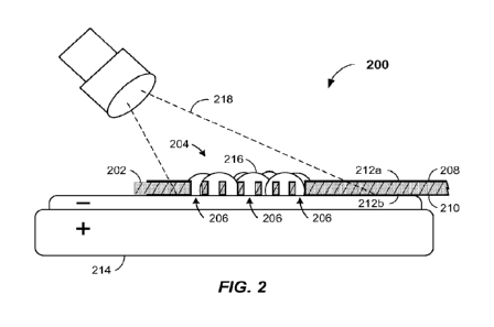
[0011] FIG. 2 illustrates a cross-sectional side view of
another portion of a
flexible PCB having a coin cell battery mounted and electrically connected
thereto
according to embodiments.
- 3 -
CA 03171398 2022- 9- 12
WO 2021/180917
PCT/EP2021/056320
[0012] FIG. 3 illustrates a flowchart of a method of mounting
a coin cell
battery to a flexible PCB according to embodiments.
[0013] FIGS. 4A and 4B illustrate a plan view of another
portion of a
flexible PCB having a plurality of slits or cuts arranged there through to
accommodate mounting and electrical connection of one or more batteries to the
flexible PCB according to embodiments.
[0014] FIG. 5 illustrates a flowchart of another method of
mounting a coin
cell battery to a flexible PCB according to embodiments.
[0015] FIG. 6A illustrates a plan view of a flexible PCB
having a foldable
arm extending therefrom according to embodiments.
[0016] FIGS. 6B and 6C illustrate plan and side views,
respectively, of the
flexible PCB of FIG. 6A with the foldable arm folded to mount and electrically
connect a pair of coin cell batteries to the flexible PCB according to
embodiments.
[0017] FIG. 7 illustrates a plan view of a flexible PCB
material configured
to fabricate flexible PCBs each having a foldable arm according to
embodiments.
[0018] FIG. 8 illustrates a plan view of a flexible PCB
having an attachable
arm to mount and electrically connect a pair of coin cell batteries to the
flexible
PCB according to embodiments.
[0019] FIG. 9 illustrates a plan view of the attachable arm
of FIG. 8
according to embodiments.
[0020] FIG. 10 illustrates a flowchart of another method of
mounting a coin
cell battery to a flexible PCB according to embodiments.
[0021] FIG. 11 illustrates a plan view of a flexible PCB
having battery
contact pads according to embodiments.
[0022] FIG. 12 illustrates a simplified plan view block
diagram of a
continuous glucose monitor (CGM) wireless transmitter having a flexible PCB
according to embodiments.
- 4 -
CA 03171398 2022- 9- 12
WO 2021/180917
PCT/EP2021/056320
DETAILED DESCRIPTION
[0023] A flexible printed circuit board (PCB) may include an
assembly of
electronic circuits and/or components surface mounted on a flexible plastic
substrate, for example. The flexible plastic substrate may be, e.g., a
polyimide,
polyether ether ketone (PEEK), a conductive transparent polyester film or the
like. Flexible PCBs are typically very thin, usually no more than a few
millimeters
thick. A flexible PCB can advantageously bend or flex during its use. In
contrast,
rigid PCBs, which are thicker than flexible PCBs, may break and/or the
circuitry
imprinted thereon may malfunction if they are bent or flexed during use.
[0024] A small battery-operated electronic device that may
benefit from
having a flexible PCB is a continuous glucose monitor (CGM) wireless
transmitter. A CGM wireless transmitter may be placed on a user's body to
automatically take glucose measurements at regular intervals and wirelessly
transmit those measurements to a receiver and/or an insulin pump. A CGM
wireless transmitter with a flexible PCB for a sensor and wireless transmitter
circuitry may allow the CGM wireless transmitter to conform to the surface of
a
user's body at the attachment site, thus improving the CGM wireless
transmitter's
adhesion thereto and/or the user's comfort while wearing the CGM wireless
transmitter. CGMs are typically powered by coin cell batteries, such as, e.g.,
miniature silver oxide batteries. However, coin cell batteries held in
conventional
coin cell battery holders, which are generally configured for mounting to
rigid
PCBs, would defeat the purpose of having a flexible PCB because the thickness
and size of the battery holders would add rigidity to the flexible PCB.
[0025] In accordance with the embodiments disclosed herein,
coin cell
batteries (and batteries with a similar configuration) may be mounted directly
to a
flexible PCB without using conventional battery holders. Such direct mounting
maintains the overall flexibility of a flexible PCB by minimizing the
additional
thickness added to the flexible PCB by the coin cell batteries. For example,
in
one embodiment, a flexible PCB having a one or more coin cell batteries
mounted directly thereon may have a maximum thickness of only about 1.6 mm,
- 5 -
CA 03171398 2022- 9- 12
WO 2021/180917
PCT/EP2021/056320
thus allowing a CGM wireless transmitter with a flexible PCB to readily
conform to
the surface of a user's body at the attachment site.
[0026] To ensure a reliable mechanical and electrical
connection between
a battery and a flexible PCB, a battery contact pad formed on the flexible PCB
and methods of connecting batteries to a flexible PCB in accordance with one
or
more embodiments are provided, as will be explained in greater detail below in
connection with FIGS. 1A-12.
[0027] FIGS. 1A and 1B illustrate a portion 100 of a flexible
PCB 102
having a battery contact pad 104 formed thereon in accordance with one or more
embodiments. Battery contact pad 104 includes a plurality of metalized vias
106
(only a few labeled in FIG. 1A) arranged in a pattern. Other suitable patterns
than the one shown may be used. Each metalized via 106 is a through hole that
extends through flexible PCB 102 from a first surface 108 to an opposite
second
surface 110 of flexible PCB 102. A conductive metal 111, such as, e.g.,
copper,
may be disposed on and over the inside surface of each metalized via 106.
Other suitable conductive metals may be used. A printed conductor 112a formed
on first surface 108 surrounds and electrically connects the plurality of
metalized
vias 106 to each other, and a printed conductor 112b formed on second surface
110 also surrounds and electrically connects the plurality of metalized vias
106 to
each other. Accordingly, the plurality of metalized vias 106 electrically
connects
printed conductors 112a and 112b to each other. Printed conductors 112a and
112b may be copper or any other electrical conductor suitable for printing on
a
flexible PCB. In some embodiments, each metalized via 106 may have a
diameter ranging from 0.5 mm to 2 mm, and battery contact pad 104 may have a
diameter ranging from 3 mm to 15 mm.
[0028] FIG. 2 illustrates a portion 200 of a flexible PCB 202
having a
battery 214 attached to a battery contact pad 204 on a bottom surface 210 of
flexible PCB 202 in accordance with one or more embodiments. Battery contact
pad 204 may be similar or identical to battery contact pad 104. Battery 214
may
be a coin cell battery and, more particularly, may be a miniature silver oxide
battery. Alternatively, battery 214 may be of another type having a similar
- 6 -
CA 03171398 2022- 9- 12
WO 2021/180917
PCT/EP2021/056320
configuration (e.g., having a flat surface). A conductive light curable epoxy,
such
as conductive ultraviolet curable epoxy 216, is disposed on top surface 208
over
and in each metalized via 206 (only three labeled in FIG. 2) such that
conductive
ultraviolet curable epoxy 216 contacts and adheres to battery 214 and provides
a
conductive path from battery 214 through the metalized vias 206 to printed
conductor 212a (and, in some embodiments, to a printed conductor 212b on
bottom surface 210). Printed conductor 212a may be connected to other
circuitry, components, or connectors (not shown) on flexible PCB 202.
Conductive ultraviolet curable epoxy 216 may be, e.g., Elecolite 3063, 3064,
or
3065 by Panacol-Elosol GmbH. Advantageously, battery 214 is mounted directly
to flexible PCB 202 without a battery holder.
[0029] FIG. 3 illustrates a method 300 of mounting a battery
to a flexible
PCB in accordance with one or more embodiments. At process block 302,
method 300 can include positioning a battery contact pad of a flexible PCB on
a
surface of a battery. As shown in FIG. 2, e.g., battery contact pad 204 of
flexible
PCB 202 may be positioned on a top surface of coin cell battery 214.
[0030] At process block 304, method 300 can include applying
conductive
ultraviolet curable epoxy to the battery contact pad such that the conductive
ultraviolet curable epoxy fills the metalized vias of the battery contact pad
and
contacts the surface of the battery. The conductive ultraviolet curable epoxy
is
used as an adhesive and/or a "cold" solder for surface mounting components,
particularly heat sensitive components, to a flexible PCB. The conductive
ultraviolet curable epoxy may be applied in any suitable manner and should at
least substantially fill enough of the metalized vias such that a sufficient
amount
contacts the surface of battery to establish a reliable mechanical and
electrical
connection between the battery and metalized vias. Referring again to FIG. 2,
conductive ultraviolet curable epoxy 216 preferably completely fills each of
metalized vias 206 and fully contacts the top surface of battery 214.
[0031] At process block 306, method 300 can include exposing
the battery
contact pad to ultraviolet light to cure the conductive ultraviolet curable
epoxy. As
shown in FIG. 2, conductive ultraviolet curable epoxy 216 covering battery
- 7 -
CA 03171398 2022- 9- 12
WO 2021/180917
PCT/EP2021/056320
contact pad 204 may be exposed to ultraviolet light 218 to cure conductive
ultraviolet curable epoxy 216, thus establishing a reliable mechanical and
electrical connection between battery 214 and metalized vias 206. Depending on
the power of the ultraviolet light, epoxy type, and ambient temperature,
curing
time may range from a few seconds to a minute or so. Once cured, a robust
conductive junction is formed between the battery and the battery contact pad.
[0032] Notably, the pattern of metalized vias on the battery
contact pad
advantageously facilitates the curing of the conductive ultraviolet curable
epoxy
such that little to no epoxy remains uncured. Uncured epoxy may weaken or
even prevent a reliable mechanical and electrical connection from forming. The
pattern of metalized vias increases the conductive area, which lowers the
total
connection resistance, and the relatively large vias allow the ultraviolet
light to
reach the bottom of the epoxy in each via (i.e., at the battery surface),
which
improves curing.
[0033] To complete the electrical connection to battery 214
shown in FIG.
2 (wherein only one terminal, e.g., the negative terminal, is shown
connected), a
second connection needs to be made to the other terminal (e.g., the positive
terminal) on the bottom surface of battery 214. FIGS. 4A, 4B, 6A-6C, and 8
illustrate several embodiments in which the second connection to the battery
can
be made while advantageously maintaining the overall flexibility of the
flexible
PCB.
[0034] FIGS. 4A and 4B illustrate a portion 400 of a flexible
PCB 402
having battery contact pads 404a-404d and a plurality of slits or cuts 420a,
420b,
and 420c arranged in flexible PCB 402 to accommodate the mounting of one or
more coin cell batteries 414a and 414b (or batteries with similar
configuration) to
flexible PCB 402 at battery contact pads 4042-404d in accordance with one or
more embodiments. Each of battery contact pads 404a-404d may be similar or
identical to battery contact pad 104. Slits 420a-420c each extend through
flexible
PCB 402 from a top surface 408 to a bottom surface (not shown in FIGS. 4A and
4B) of flexible PCB 402. Slits 420a-420c may be made in any suitable manner.
Slits 420a and 420b form a first section 422 that includes battery contact
pads
- 8 -
CA 03171398 2022- 9- 12
WO 2021/180917
PCT/EP2021/056320
404a and 404b, and slits 420b and 420c form a second section 424 that includes
battery contact pads 404c and 404d. First section 422 is separated from second
section 424 by slit 420b.
[0035] As shown in FIG. 4B, battery 414a may be inserted in
slit 420b and
through slit 420a such that one surface of battery 414a (e.g., the negative
terminal surface as shown) contacts the bottom surface of first section 422
under
battery contact pad 404a (and its metalized vias) and the opposite surface
(e.g.,
the positive terminal surface) contacts the top surface 408 of second section
424
over battery contact pad 404c (and its metalized vias). Similarly, battery
414b
may be inserted in slit 420b and through slit 420a such that one surface of
battery
414a (e.g., the positive terminal surface as shown) contacts the bottom
surface of
first section 422 under battery contact pad 404a (and its metalized vias) and
the
opposite surface (e.g., the negative terminal surface) contacts the top
surface
408 of second section 424 over battery contact pad 404c (and its metalized
vias).
[0036] To form mechanical and electrical connections between
batteries
414a and 414b and battery contact pads 404a-404d, conductive ultraviolet
curable epoxy may be disposed over and in each plurality of metalized vias of
battery contact pads 404a-404d such that the conductive ultraviolet curable
epoxy contacts and, after curing by ultraviolet light, adheres to each battery
414a
and 414b and provides a conductive path from each battery 414a and 414b to its
respective pair of battery contact pad 404a-404d (and plurality of metalized
vias),
as similarly shown, e.g., in FIG. 2, and as described below in connection with
FIG. 5.
[0037] Note that in some embodiments, depending on the
configuration of
imprinted and/or mounted circuitry and/or components (not shown) on flexible
PCB 402, batteries 414a and 414b may instead be inserted under second section
424 to contact battery contact pads 404a-404d in an opposite manner as that
shown in FIG. 4B.
- 9 -
CA 03171398 2022- 9- 12
WO 2021/180917
PCT/EP2021/056320
[0038] Note also that printed conductors (not shown) may
electrically
connect battery contact pads 404a-404d to other circuitry and/or components
imprinted and/or mounted on flexible PCB 402.
[0039] Note further that although two batteries 414a and 414b
are shown,
in other embodiments portion 400 and slits 420a-420c may be configured to
accommodate just a single coin cell battery, depending on the power needs of
the circuitry and/or components imprinted and/or mounted on flexible PCB 402.
[0040] FIG. 5 illustrates a method 500 of mounting a coin
cell battery (or
battery with a similar configuration) to a flexible PCB having a plurality of
slits for
accommodating the battery in accordance with one or more embodiments. At
process block 502, method 500 can include providing a flexible PCB having at
least two battery contact pads and a plurality of slits arranged to
accommodate at
least one battery. For example, as shown in FIG. 4A, flexible PCB 402 may be
provided with battery contact pads 404a-404d and a plurality of slits 420a,
420b,
and 420c arranged to accommodate one or more coin cell batteries 414a and/or
414b.
[0041] At process block 504, method 500 can include inserting
a battery in
one or more slits such that the battery contacts one battery contact pad on
one
surface of the battery and contacts another battery contact pad on an opposite
surface of the battery. For example, as shown in FIG. 4B, battery 414a may be
inserted in slit 420b and through slit 420a such that one surface of battery
414a
(e.g., the negative terminal surface as shown) contacts battery contact pad
404a
(and its metalized vias) and the opposite surface (e.g., the positive terminal
surface) of battery 414a contacts battery contact pad 404c (and its metalized
vias).
[0042] At process block 506, method 500 can include applying
conductive
ultraviolet curable epoxy to the accessible side of each contact pad such that
the
epoxy fills the metalized vias of each contact pad and contacts the battery
surface. For example, referring to FIGS. 2, 4A, and 4B, a first conductive
ultraviolet curable epoxy (such as, e.g., conductive ultraviolet curable epoxy
216)
- 10 -
CA 03171398 2022- 9- 12
WO 2021/180917
PCT/EP2021/056320
may be applied on top surface 408 of first section 422 over and in battery
contact
pad 404a (and its metalized vias) such that the first conductive ultraviolet
curable
epoxy contacts the negative terminal surface of battery 414a. Furthermore, a
second conductive ultraviolet curable epoxy (such as, e.g., conductive
ultraviolet
curable epoxy 216) may be applied on a bottom surface of second section 424
(not shown in FIG. 4B) over and in battery contact pad 404c (and its metalized
vias) such that the second conductive ultraviolet curable epoxy contacts the
positive terminal surface of battery 414a (not shown in FIG. 4B).
[0043] At process block 508, method 500 can include exposing
each
battery contact pad to ultraviolet light to cure the conductive ultraviolet
curable
epoxy. Referring to FIG. 4B and continuing with the above example, the first
conductive ultraviolet curable epoxy over and in battery contact pad 404a may
be
exposed to ultraviolet light (such as, e.g., ultraviolet light 218 of FIG. 2)
to cure
the first conductive ultraviolet curable epoxy, thus establishing a reliable
mechanical connection between the negative terminal surface of battery 414a
and battery contact pad 404a (i.e., the cured epoxy adheres to the battery
surface and metalized vias). A conductive path from the negative terminal
surface of battery 414a to and through battery contact pad 404a (by way of its
metalized vias) is also established. Similarly, the second conductive
ultraviolet
curable epoxy over and in battery contact pad 404c may be exposed to
ultraviolet
light (such as, e.g., ultraviolet light 218 of FIG. 2) to cure the second
conductive
ultraviolet curable epoxy, thus establishing a reliable mechanical connection
between the positive terminal surface of battery 414a and battery contact pad
404c. A conductive path from the positive terminal surface of battery 414a to
and
through battery contact pad 404c (by way of its metalized vias) is also
established. Note that the first and second conductive ultraviolet curable
epoxies
may be exposed to ultraviolet light sequentially or concurrently (e.g., by one
ultraviolet lighting device directed at top surface 408 and another
ultraviolet
lighting device directed at the bottom surface (not shown) of flexible PCB
402).
[0044] FIGS. 6A-6C illustrate a flexible PCB configuration
600 having a
foldable arm 626 configured to mount and electrically connect a pair of coin
cell
- 11 -
CA 03171398 2022- 9- 12
WO 2021/180917
PCT/EP2021/056320
batteries 614a and 614b (or batteries with a similar configuration) to a
flexible
PCB 602 in accordance with one or more embodiments. As shown in FIG. 6A,
flexible PCB 602 initially has folding arm 626 extending therefrom. Foldable
arm
626 may have battery contact pads 604a and 604b formed therein that may be
connected to each other by a printed conductor 612a on one surface of foldable
arm 626 and, in some embodiments, by a printed conductor 612b on the opposite
surface of foldable arm 626 (see FIG. 6B). Each of battery contact pads 604a
and 604b may be similar or identical to battery contact pad 104. Flexible PCB
602 may have one or more coin cell batteries 614a and 614b placed on a top
surface 608 of flexible PCB 602 over respective battery contact pads 604c and
604d (see FIG. 6C) formed in flexible PCB 602. Each of battery contact pads
604c and 604d may also be similar or identical to battery contact pad 104. In
those embodiments where only a single battery is required, foldable arm 626
and
flexible PCB 602 may each have just one appropriately positioned battery
contact
pad, and the length of foldable arm 626 may be adjusted accordingly.
[0045] In those embodiments where some rigidity to the area
where the
battery or batteries are to be mounted is desired to facilitate an assembly
process
of flexible PCB 602, a non-conductive battery stiffener 628 may be used to
hold
batteries 614a and 614b. Battery stiffener 628 may have a height or thickness
no
greater than the height or thickness of batteries 614a and 614b. Any suitable
non-conductive material (e.g., a rigid plastic) may be used to make battery
stiffener 628. Battery stiffener 628 may advantageously provide rigidity to
the
battery mounting area without increasing the height of the PCB assembly of
batteries, circuits, and/or components. The flexibility of the remaining
portion of
flexible PCB 602 is not adversely affected by battery stiffener 628.
[0046] FIGS. 6B and 6C illustrate flexible PCB 602 having
foldable arm
626 folded over and onto batteries 614a and 614b. In some embodiments, the
radius R at the fold of foldable arm 626 may be about 1.5 mm (-F1- 0.1 mm).
Foldable arm 626 is configured to fold over onto only one surface of flexible
PCB
602 (e.g., onto top surface 608 as shown). That is, foldable arm 626 is
fabricated
with a pre-cut to fold onto either the top or bottom surface of flexible PCB
602,
- 12 -
CA 03171398 2022- 9- 12
WO 2021/180917
PCT/EP2021/056320
but not both. Foldable arm 626 may be mechanically and electrically connected
to batteries 614a and 614b by application and curing of conductive ultraviolet
curable epoxy 616 disposed over and in each of battery contact pads 604a and
604b from the top surface of foldable arm 626 (as shown in FIG. 6C) in a same
or
similar manner as described above in connection with FIGS. 2, 3, 4B, and 5.
Likewise, batteries 6142 and 614b may be mechanically and electrically
connected to top surface 608 of flexible PCB 602 by application and curing of
conductive ultraviolet curable epoxy 616 disposed over and in each of battery
contact pads 604c and 604d from a bottom surface 610 of flexible PCB 602 in a
same or similar manner as described above in connection with FIGS. 2, 3, 4B,
and 5. Note that the curing of conductive ultraviolet curable epoxies 616 in
and
over battery contact pads 604a-604d by ultraviolet light may be performed
concurrently or in any suitable order.
[0047]
FIG. 7 illustrates a flexible PCB material 700 configured to optimize
an automated fabrication of a flexible PCB having a foldable arm, such as,
e.g.,
flexible PCB 602, in accordance with one or more embodiments. As shown,
flexible PCB material 700 may be configured to have a closely arranged
grouping
of flexible PCBs 702a-702d to minimize unused PCB material. Each flexible PCB
702a-702d may have four battery contact pads 704a-704d (only one group of
battery contact pads is labeled in FIG. 7) to accommodate two coin cell (or
similarly configured) batteries. Other embodiments configured for a single
battery
may only have two battery contact pads, such as, e.g., battery contact pad
704a
and 704d. Each of battery contact pads 704a-704d may be similar or identical
to
battery contact pad 104. Each flexible PCB 702a-702d may also have a foldable
arm 726 (only one labeled), which may be similar or identical to foldable arm
626.
Each flexible PCB 702a-702d may further have printed conductors 712a and
712b (only one each labeled), wherein printed conductor 712a is formed on one
surface of foldable arm 726 to connect battery contact pads 704c and 704d to
each other, and a printed conductor 712b is formed on an opposite surface of
foldable arm 726 to also connect battery contact pads 704c and 704d to each
other. Although a single column of four flexible PCBs 702a-702d is shown in
- 13 -
CA 03171398 2022- 9- 12
WO 2021/180917
PCT/EP2021/056320
FIG. 7, other embodiments of PCB material may have other numbers of columns
and/or closely arranged groupings of flexible PCBs based on the configuration
shown.
[0048] FIG. 8 illustrates a flexible PCB configuration 800
having an
attachable arm 826 configured to mount and electrically connect a pair of coin
cell batteries 814a and 814b (or batteries with a similar configuration) to a
flexible
PCB 802 in accordance with one or more embodiments. Batteries 814a and
814b may be placed on a top surface 808 of flexible PCB 802 over respective
battery contact pads (not shown) formed in flexible PCB 802. Each of the
battery
contact pads formed in flexible PCB 802 may be similar or identical to battery
contact pad 104 of FIGS. 1A and 1B. In those embodiments where some rigidity
to the area where the battery or batteries are to be mounted is desired to
facilitate
an assembly process of flexible PCB 802, a non-conductive battery stiffener
828
may be used to hold batteries 814a and 814b. Battery stiffener 828 may be
identical or similar to battery stiffener 626 of FIG. 6.
[0049] As shown in FIG. 9, attachable arm 826 is a separate
part that may
have battery contact pads 904a and 904b formed therein that may be connected
to each other by a printed conductor 912a on one surface of attachable arm 826
and, in some embodiments, by a printed conductor (not shown) on the opposite
surface of attachable arm 826. Each of battery contact pads 904a and 904b may
be similar or identical to battery contact pad 104. Attachable arm 826 may
also
have a single-ended termination 930 formed at one end of attachable arm 826
that is configured to be inserted into a connector 832 mounted on top surface
808
of flexible PCB 802. In the two-battery embodiment shown in FIG. 8, the
connection of single-ended termination 930 to connector 832 may be just a
physical connection (no electrical connection at connector 832). In other
embodiments using only a single battery, the connection of single-ended
termination 930 to connector 832 may be a physical and electrical connection
(to
complete the circuit with the single battery) wherein attachable arm 826 may
include a printed conductor extending from the battery contact pad to the
single-
ended termination 930 for an electrical connection from the top surface
terminal
- 14 -
CA 03171398 2022- 9- 12
WO 2021/180917
PCT/EP2021/056320
of the battery through connector 832 to circuitry imprinted on top surface
808. In
some embodiments, connector 832 may be an FPC (flexible printed circuit)
connector. Other suitable connectors may be used. The shape of attachable
arm 826 and the placement of connector 832 on top surface 808 are configured
such that attachable arm 826 when inserted in connector 832 has battery
contact
pad 904a positioned over and on battery 8142 and battery contact pad 904b
positioned over and on battery 814b. Other shapes of attachable arm 826 and
placements of connector 832 are possible. In those embodiments where only a
single battery is used, attachable arm 826 and flexible PCB 802 may each have
just one appropriately positioned battery contact pad, and the length and/or
shape of attachable arm 826 and the placement of connector 832 may be
adjusted accordingly. Attachable arm 826 may be made of the same flexible
PCB material as flexible PCB 802. Alternatively, other suitable materials may
be
used to fabricate attachable arm 826.
[0050] To complete the mechanical and electrical connections
of
attachable arm 826 to batteries 814a and 814b, conductive ultraviolet curable
epoxy, such as, e.g., conductive ultraviolet curable epoxy 216 or 616, may be
disposed over and in each of battery contact pads 904a and 904b from a top
surface 908 of attachable arm 826 and cured in a same or similar manner as
described above in connection with FIGS. 2, 3, 4B, 5, and 6C. Likewise,
batteries 814a and 814b may be mechanically and electrically connected to top
surface 808 of flexible PCB 802 by application and curing of conductive
ultraviolet
curable epoxy disposed over and in each of the battery contact pads formed in
flexible PCB 802 from a bottom surface of flexible PCB 802 in a same or
similar
manner as described above in connection with FIGS. 2, 3, 4B, 5, and 6C. Note
that the curing of conductive ultraviolet curable epoxies in and over battery
contact pads 904a, 904b, and the two battery contact pads formed in flexible
PCB 802 by ultraviolet light may be performed concurrently or in any suitable
order.
[0051] FIG. 10 illustrates a method 1000 of mounting a coin
cell (or
similarly configured) battery to a flexible PCB with an arm in accordance with
one
- 15 -
CA 03171398 2022- 9- 12
WO 2021/180917
PCT/EP2021/056320
or more embodiments. At process block 1002, method 1000 can include
providing a flexible PCB having at least one battery contact pad formed
therein.
For example, as shown in FIG. 11, flexible PCB 1102 may have one or more
battery contact pads 1104a and/or 1104b formed therein. Each of battery
contact
pads 1104a and 1104b may be similar or identical to battery contact pad 104.
[0052] At process block 1004, method 1000 can include
positioning at
least one coin cell battery (or battery of similar configuration) on the
flexible PCB
over the at least one battery contact pad. If more than one battery is to be
mounted on the flexible PCB, each battery is to be positioned over a
respective
battery contact pad. For example, as shown in FIGS. 6A, 6B, and 8, one or more
batteries 614a, 614b, 814a, and/or 814b may be positioned on flexible PCB 602
or 802 over a respective battery contact pad. If two batteries (e.g.,
batteries 614a
and 614b or batteries 814a and 814b) are to be positioned, battery stiffener
628
or 828 may be used, if desired, to add rigidity to the battery mounting area
of the
flexible PCB.
[0053] At process block 1006, method 1000 can include
positioning an arm
over and on the at least one battery, the arm having at least one battery
contact
pad formed therein and positioned over and on the at least one battery. If
more
than one battery is to be mounted on the flexible PCB, the arm has a
respective
battery contact pad formed therein for each battery. The battery contact pads
are
appropriately spaced apart from each other on the arm to accommodate
positioning over respective batteries under the arm. One or more printed
conductors formed on the arm may electrically connect the battery contact pads
to each other. Referring to FIGS. 6A- 6C, 8, and 9, the arm may be, e.g.,
foldable arm 626 or attachable arm 826. In those embodiments where the arm is
foldable arm 626, method 1000 at process block 1006 includes folding the arm
such that foldable arm 626 is positioned over and on the at least one battery
and
the one or more battery contact pads of foldable arm 626 are positioned over
and
on the one or more batteries, respectively, as shown in FIGS. 6B and 6C. In
those embodiments where the arm is attachable arm 826, method 1000 at
process block 1006 includes inserting the single-ended termination 930 of
- 16 -
CA 03171398 2022- 9- 12
WO 2021/180917
PCT/EP2021/056320
attachable arm 826 in connector 832 such that attachable arm 826 is positioned
over and on the at least one battery and the one or more battery contact pads
of
attachable arm 826 are positioned over and on the one or more batteries,
respectively, as shown in FIG. 8.
[0054] At process block 1008, method 1000 can include
applying
conductive ultraviolet curable epoxy to the accessible side of each contact
pad
such that the epoxy fills the metalized vias of each contact pad and contacts
the
battery surface, as similarly described above in connection with process block
506 of method 500 (FIG. 5).
[0055] And at process block 1010, method 1000 can include
exposing
each battery contact pad to ultraviolet light to cure the conductive
ultraviolet
curable epoxy, as similarly described above in connection with process block
508
of method 500 (FIG. 5). Mechanical and electrical connections between the
battery and the battery contact pads formed in the arm and flexible PCB are
thus
established.
[0056] FIG. 12 illustrates a continuous glucose monitor (CGM)
wireless
transmitter 1200 having a flexible PCB in accordance with one or more
embodiments. CGM wireless transmitter 1200 includes a flexible PCB 1202
having one or more batteries 1204 mounted thereon. One or more batteries
1204 may be mounted on and electrically connected to flexible PCB 1202 in any
manner shown in FIGS. 2, 4B, 6B, 6C, and/or 8. CGM wireless transmitter 1200
also includes a glucose sensor 1234 and wireless transmitter circuitry 1236
each
fabricated on top surface 1208 (or alternatively on a bottom surface) of
flexible
PCB 1202 and electrically connected to each other, to one or more batteries
1204, and to possibly other circuits or components (not shown) by printed
conductors 1212a, 1212b, and 1212c. A portion of glucose sensor 1234 is
inserted into the skin of a user's body and may be configured to continually
measure glucose levels, and wireless transmitter circuitry 1236 may be
configured to wirelessly transmit those glucose measurements to a CGM receiver
and/or insulin pump. Other circuits and circuit components (not shown) may
also
be fabricated on flexible PCB 1202. Advantageously, CGM wireless transmitter
- 17 -
CA 03171398 2022- 9- 12
WO 2021/180917
PCT/EP2021/056320
1200 is capable of bending and/or flexing such that it may conform to a
surface of
the user's body to which it is attached, improving the adherence of CGM
wireless
transmitter 1200 to the skin surface and/or the user's comfort while wearing
CGM
wireless transmitter 1200.
[0057] In some embodiments, other light curable epoxies may
be
employed, such as epoxies that are curable at other wavelengths (e.g.,
wavelengths for middle-ultraviolet light, near-ultraviolet light, violet
light, blue light,
etc., or other visible wavelengths). For example, in some embodiments, methods
300, 500, 1000, may be employed with other light curable epoxies, as may any
of
the circuit board configurations described herein.
[0058] While the disclosure is susceptible to various
modifications and
alternative forms, specific method and apparatus embodiments have been shown
by way of example in the drawings and are described in detail herein. It
should
be understood, however, that the particular methods and apparatus disclosed
herein are not intended to limit the disclosure but, to the contrary, to cover
all
modifications, equivalents, and alternatives falling within the scope of the
claims.
- 18 -
CA 03171398 2022- 9- 12