Note: Descriptions are shown in the official language in which they were submitted.
CA 03171980 2022-08-18
WO 2021/170543 PCT/EP2021/054363
A THERMAL INKJET PRINTHEAD, AND A PRINTING ASSEMBLY
AND PRINTING APPARATUS COMPRISING THE SAME
FIELD OF THE INVENTION
[0001] The present invention relates to the field of thermal inkjet printing
technology, and in
particular, to a thermal inkjet printhead.
BACKGROUND OF THE INVENTION
[0002] Thermal inkjet printing technology has been relatively well developed.
There have
been various thermal inkjet printheads. For example, US6123419A discloses a
thermal inkjet
printhead employing a higher resistance value segmented heater resistor in
order to overcome
inefficient power dissipation in parasitic resistances. US6582062B1 discloses
a large array
inkjet printhead employing a multiplexing device to reduce parasitic
resistance and the number
of incoming leads.
[0003] In a thermal inkjet printhead, ejection of an ink drop through a nozzle
is accomplished
by quickly heating a volume of ink residing within an ink ejection chamber,
and heating of the ink
is accomplished by a short current pulse applied to a heater resistor
positioned within the ink
ejection chamber. The heating of the ink causes an ink vapor bubble to form
and expand rapidly,
thus forcing the liquid ink through the nozzle. Once the pulse ends and an ink
drop is ejected,
the ink ejection chamber refills with ink by an ink channel. The heater
resistor is made of a
resistive film, and a thermal inkjet printhead comprises a plurality of such
heater resistors as a
resistor array. The heater resistors are electrically connected to associated
logic circuitry and
power circuitry by conducting traces and/or pads so that each of the heater
resistors can be
controlled appropriately. In implementing the logic circuitry and power
circuitry, metal lines are
used.
[0004] In the prior art thermal inkjet printhead device, usually all the
heater resistors are
covered by a continuous protective layer, which prevents the underlying
resistive films from
1
CA 03171980 2022-08-18
WO 2021/170543 PCT/EP2021/054363
being damaged by abrupt collapse of ink vapor bubbles during operation of the
printhead. For
this purpose, some refractory metal, like Tantalum, is used for the protective
layer, which shows
both great mechanical strength and good thermal conductivity. Such a Tantalum
film is
commonly deposited continuously in the entire resistor area, spanning the
whole resistor array.
Because of the electrical conductivity of Tantalum, a large area of the device
turns out to be
covered by the continuous Tantalum conductive film. On one hand, since voltage
levels in metal
lines across the device do change in time, this Tantalum conductive film could
be capacitively
coupled with the neighboring metal lines beneath it and therefore it could
cause some issue with
the logical circuitry. On the other hand, possible pinholes or discontinuities
in a dielectric layer
interposed between the Tantalum layer and the underlying metal lines could
give rise to parasitic
electrical shorting paths, whose effect could cause both electrical drawbacks
and
electrochemical effects through ink. US 6 441 838 B1 discloses such an ink jet
printhead
comprising a tantalum passivation layer to provide mechanical passivation for
the ink firing
resistors by absorbing the cavitation pressure of the collapsing drive bubble,
where the tantalum
passivation layer is disposed over the heater resistors, extending beyond the
ink chambers and
over associated ink channels.
SUM MARY OF THE INVENTION
[0005] It is an object of the present invention to provide a solution that can
alleviate or solve at
least some of the above problems in the prior art. The mentioned problems are
solved by the
subject-matter of the independent claims. Further preferred embodiments are
defined in the
dependent claims.
[0006] According to an aspect of the present invention, there is provided a
thermal inkjet
printhead, which comprises:
a substrate;
a nozzle layer, including a plurality of nozzles formed therethrough;
2
CA 03171980 2022-08-18
WO 2021/170543 PCT/EP2021/054363
a plurality of ink ejection chambers corresponding to the plurality of
nozzles;
a plurality of heater resistors formed on the substrate and corresponding to
the plurality of
ink ejection chambers, each of the heater resistors being located in a
different one of the ink
ejection chambers so that ink drop ejection through each of the nozzles is
caused by heating of
one of the heater resistors that is located in the corresponding ink ejection
chamber;
a plurality of separated cavitation islands formed on and corresponding to the
plurality of
heater resistors, each of the cavitation islands covering a different one of
the heater resistors;
and
a dielectric layer interposed between the heater resistors and the cavitation
islands,
wherein the dielectric layer is a composite film made of Silicon nitride and
Silicon carbide and
having a thickness in the range of about 0.4 to about 0.65 pm.
[0007] According to another aspect of the present invention, there is provided
a printing
assembly comprising the thermal inkjet printhead described above.
[0008] According to yet another aspect of the present invention, there is
provided a printing
apparatus, for example, a printer, comprising the thermal inkjet printhead
described above.
[0009] With the solution of the present invention, overlapping of each
cavitation island with its
neighboring circuitry can be reduced, and therefore the likelihood of
generating parasitic
capacitive coupling between the cavitation layer and its neighboring circuitry
is dramatically
reduced compared with that with the prior art. Moreover, due to the relatively
small surface area
of a single cavitation island, it is less likely that the cavitation island
overlaps with a possible
defect in the thin dielectric film beneath it, i.e., the probability that a
defect in the dielectric film
lies just below some cavitation island and thus causes some electrical short
circuit is reduced.
Thus, due to the specific composition and thickness of the dielectric layer
(which is far thinner
than the ones in the prior art), providing the "electrically" insulated
cavitation islands is clearly
advantageous. As a result, the present invention provides an optimized heat
transfer with a
3
CA 03171980 2022-08-18
WO 2021/170543 PCT/EP2021/054363
reduced risk to have pinholes with unwanted conductive bridges between
different layers.
Therefore, using the present invention can help to substantially improve the
printhead reliability,
increasing in turn the yield of the manufacturing process.
BRIEF DESCRIPTION OF THE DRAWINGS
[0010] Non-limiting and non-exhaustive embodiments of the present invention
are described
by way of example with reference to the following figures, in which:
[0011] Fig. 1 is a schematic diagram illustrating an exemplary layout of a
thermal inkjet
printhead according to an embodiment of the present invention;
[0012] Fig. 2 is a schematic diagram illustrating an exemplary wafer before
being diced;
[0013] Fig. 3 schematically illustrates a perspective view of an exemplary
printing assembly
incorporating the thermal inkjet printhead of the present invention;
[0014] Fig. 4 schematically illustrates a portion of an exemplary microfluidic
circuit in a
perspective view;
[0015] Fig. 5 schematically illustrates a portion of the microfluidic circuit
in Fig. 4 in a
cross-sectional view;
[0016] Fig. 6 is a cross-sectional view schematically illustrating a
portion of Fig. 5 in more
detail;
[0017] Fig. 7 schematically illustrates a portion of the thermal inkjet
printhead in Fig. 1;
[0018] Fig. 8 schematically illustrates a portion of a thermal inkjet
printhead of the prior art;
[0019] Fig. 9a, Fig. 9b and Fig. 9c illustrate a possible situation for the
thermal inkjet
printhead whose portion is illustrated in Fig. 8, an equivalent circuit
corresponding to the
situation, and a modified version of the equivalent circuit, respectively; and
[0020] Fig. 10a, Fig. 10b and Fig. 10c illustrate another possible situation
for the thermal
inkjet printhead whose portion is illustrated in Fig. 8, one possible
equivalent circuit
corresponding to the situation, and another possible equivalent circuit
corresponding to the
4
CA 03171980 2022-08-18
WO 2021/170543 PCT/EP2021/054363
situation, respectively.
DETAILED DESCRIPTION OF THE EMBODIMENTS
[0021] In order to make the above and other features and advantages of the
present
invention more apparent, the present invention is further described below in
conjunction with the
accompanying drawings. It is to be understood that the specific embodiments
given herein are
for the purpose of explaining to those skilled in the art, and are only
illustrative but not
restrictive.
[0022] Fig. 1 schematically illustrates an exemplary layout of a thermal
inkjet printhead
according to an embodiment of the present invention. The thermal inkjet
printhead in Fig. 1
comprises a substrate 1, which is provided on its surface with a plurality of
heater resistors 2,
arranged in one or more columns 3. The thermal inkjet printhead may be in the
form of a chip.
As shown in Fig. 2, multiple such chips, each being carried by a substrate 1,
can be
manufactured in a single silicon wafer 5, which is subsequently diced into
individual chips, using
a proper semiconductor technology, including thin film deposition,
photolithography, wet and dry
etching techniques, ion implantation, oxidation, etc. The columns of the
heater resistors 2 can
be positioned in close proximity to a through-slot 4 made in an internal part
of the printhead chip
to allow ink refilling. Each of the heater resistors 2 can be made of a
resistive film, and can be
contacted with corresponding conducting trace(s). In a peripheral region of
the printhead, there
may be a set of contact pads 6, which are bonded to a flexible printed
circuit, normally using a
TAB (Tape Automated Bonding) process. Each of the heater resistors can be
electrically
connected to the flexible printed circuit via corresponding conducting
trace(s) and
corresponding contact pad(s) 6. In an active part 10 of the substrate 1, there
can be present
arrays of MOS transistors 11 for addressing of the resistors, one or more
logic circuitries 12, one
or more programmable memories 13 and other possible components, especially
when the
electronic layout associated with the heater resistors becomes relatively
complex as the number
CA 03171980 2022-08-18
WO 2021/170543 PCT/EP2021/054363
of the heater resistors increases. In addition to the resistive films forming
the heater resistors,
the thermal inkjet printhead of the present application can comprise other
layers/films, which will
be described later.
[0023] With reference to Fig. 3, which shows a printing assembly incorporating
the present
invention, a flexible printed circuit 7 is attached to a printhead cartridge
body 8, and a thermal
inkjet printhead of the present invention can be mounted and connected to the
printhead
cartridge body 8. The flexible printed circuit 7 is provided with larger
contact pads 9 to exchange
electrical signals with a printer used with the thermal inkjet printhead. The
thermal inkjet
printhead, for example, the one shown in Fig.1, can be mounted and connected
to the printhead
cartridge body 8 in any suitable manner.
[0024] With reference to Fig. 4 and Fig. 5, on the substrate surface of the
thermal inkjet
printhead of the present invention, where a stack of resistive, conductive and
dielectric films
have been deposited and patterned, as schematically represented at the region
14, a
microfluidic circuit can be deposited and realized so that ink can flow in the
deposited
microfluidic circuit through suitable channels 15 and arrive at an ink
ejection chamber 16, whose
walls surround a corresponding heater resistor 2. The channels 15 are in fluid
communication
with the through-slot 4, which can lead to an ink reservoir (not illustrated).
The microfluidic
circuit is often patterned in a suitable polymeric layer 17 called a barrier
layer. A nozzle layer 18,
for example in the form of a plate, is provided above the barrier layer. A
plurality of nozzles 19,
each being aligned with an underlying heater resistor, can be formed through
the nozzle plate
18, and from the nozzles, ink droplets 20 are ejected. During operation of the
thermal inkjet
printhead, if a heater resistor 2 is required to be activated, a short current
pulse is applied to
heat the resistor, which in turn causes vaporization of a thin layer of ink
just above the resistor
and thus forming of a vapor bubble 21. The pressure in the vaporized layer
increases suddenly,
causing ejection of a portion of the overlying liquid ink from the
corresponding nozzle above the
6
CA 03171980 2022-08-18
WO 2021/170543 PCT/EP2021/054363
activated resistor. The ink droplet travels toward a medium (e.g., a piece of
paper), producing an
ink dot on the medium's surface. After that, new ink is drawn into the ink
ejection chamber 16, to
replace the ejected droplet, until a steady state is reached.
[0025] To optimize energy transfer from the heater resistor 2 (heated by the
current pulse
through Joule effect) to the ink, it is necessary that the resistor is
thermally insulated from the
substrate, so that the heat flow takes place preferably towards the overlying
ink, which is in turn
separated from the resistive film layer by a thin dielectric film to avoid
electrical leakage. The
substrate can be made of silicon, which has an appreciable thermal
conductivity, in which case,
it is necessary to interpose an insulating layer with enough thickness between
the substrate and
the resistor: in other words, the resistor should be deposited over a suitable
insulating layer
grown or deposited onto the substrate. Thermally grown silicon oxide and BPSG
(Boron
Phosphorus Silicon Glass), produced with high-temperature processes, are both
suitable
materials for thermal insulation of the resistor, and can be used alone or in
combination. Since
the temperature for growth or deposition and/or annealing of these materials
is higher than the
operating temperature of the heater resistors in the printhead, they will
remain stable during
normal operation of the printhead.
[0026] The resistive film, which undergoes rapid and large temperature changes
during
operation of the printhead, should have stable properties and a good
resistance to a
thermo-mechanical stress. Typically, the resistance value of a heater resistor
2 is several tens
Ohms; a square-shaped heater resistor with a resistance of about 30 Ohms is
often adopted,
although different shapes and different resistance values can be adopted. A
widespread and
long-lasting choice for the heater resistor is a composite film made of
Tantalum-Aluminum alloy:
a film thickness of about 900 Angstrom gives a sheet resistance of 30 Ohms-per-
square, i.e. a
square-shaped resistor made of such a film has a resistance of 30 Ohms.
According to a
preferable embodiment of the present invention, the heater resistors are U-
shaped heater
7
CA 03171980 2022-08-18
WO 2021/170543 PCT/EP2021/054363
resistors, which means that there is a gap between nearby conductors biased at
different
voltages.
[0027] Various known solutions to address and drive multiple heater resistors
are available. If
the number of the nozzles in the printhead is relatively low, up to several
tens, each heater
resistor can be connected directly through an electrical track to a
corresponding contact pad,
while the return of current can be commonly collected by one or a few ground
pads. As the
number of the nozzles increases, direct individual driving, which necessitates
a large number of
contact pads for addressing the resistors, is difficult to realize: in fact,
the pads are usually
distributed along an outer border of the printhead chip and the number thereof
cannot increase
without any limit. A more practical solution is adopting an addressing matrix,
which allows
driving of a great number of resistors using a reduced number of contact pads.
The addressing
matrix is preferably realized with a plurality of MOS transistors, each of
which is in electrical
communication with a determined heater resistor. Individual heater resistors
can be connected
to electrodes of the transistor matrix in a suitable way so that they can be
activated on demand,
causing ejection of ink droplets from the printhead.
[0028] As indicated above, the dielectric layer above the heater resistor
provides electrical
insulation to the ink: generally, a silicon nitride film, alone or in
combination with silicon carbide,
is used to form the dielectric layer for this purpose. The insulating film for
the dielectric layer
should be thin enough to allow a strong heat flow while enduring thermo-
mechanical stresses
experienced during operation of the printhead as well as shocks due to the
bubble collapse.
According to the present invention, the dielectric layer is a composite film
made of Silicon nitride
and Silicon carbide, whose thickness is, at least, 4000 Angstrom (0.4 pm) and,
at most, 6500
Angstrom (0.65 pm). In fact, rapid expansion of the vapor bubble due to
heating of the heater
resistor has the effect of largely reducing the bubble's internal pressure, to
a level well below the
external atmospheric pressure. At the maximum of the bubble's expansion, the
bubble turns out
8
CA 03171980 2022-08-18
WO 2021/170543 PCT/EP2021/054363
to be a cavity with a low pressure inside, limited in its lower portion by the
ink ejection chamber's
floor and surrounded by ink. The larger external atmospheric pressure pushes
back the liquid
ink lying above the cavity, causing a violent impact against the chamber's
floor. This impact,
which is consequent to the collapse of the cavity previously formed in the
ink, can damage the
films which constitute the chamber's floor, i.e. the resistive film and the
overlying insulating film.
Often the thin insulating film is not sufficiently strong and an additional
protective film, called a
cavitation layer, for example made of a refractory metal, like Tantalum, is
deposited above the
insulating film. The Tantalum film is thermally conductive and strong heat
flux from the resistive
film towards the ink is maintained, even though the additional layer is
present. According to the
present invention, a novel arrangement for the cavitation layer is proposed.
The concept is to
reduce the area of the film surface of the cavitation layer without affecting
its function. In
particular, the cavitation layer can consist of a plurality of separated
cavitation islands, each
being patterned above a corresponding one of the heater resistors. Such a
cavitation layer will
be further described later with reference to Fig. 7.
[0029] The schematic representation of the region 14 in Fig. 5, comprising the
resistive layer,
the dielectric layer and the cavitation layer, can be observed in more detail
in the cross-sectional
view of Fig. 6. Below the barrier layer 17 there is the cavitation layer 22,
which is deposited onto
the dielectric film 23 as a protection. In the heater resistor area shown, the
dielectric film 23 is
placed directly onto the resistive film 24, while just outside the heater
resistor, where conductive
metal lines 25 are realized, the dielectric film 23 is deposited above
conductors. In a preferred
embodiment, the cavitation layer is made of Tantalum, but other choices can be
made, and such
choices may be known in the art.
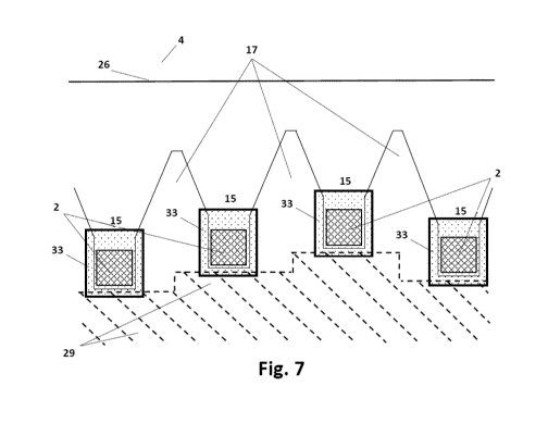
[0030] Fig. 7 schematically illustrates a portion of the thermal inkjet
printhead in Fig. 1. As
shown in Fig. 7, a series of heater resistors 2 are surrounded by the barrier
layer 17 so that
each of the heater resistors 2 is housed in an ink ejection chamber defined by
two vertical walls
9
CA 03171980 2022-08-18
WO 2021/170543 PCT/EP2021/054363
of the barrier layer 17. Ink flows from an edge 26 of the through-slot 4
through the channels 15
towards the ink injection chambers. In this embodiment, the slot edge is a
straight line, but the
edge shape which follows the staggered placement of the heater resistors, so
as to equalize the
refilling time for all of them, can be adopted.
[0031] In Fig. 7, a plurality of cavitation islands 33, which collectively
constitute a cavitation
layer together, are shown. Such a cavitation layer can be referred to as a
split cavitation layer or
a segmented cavitation layer, and each of the cavitation islands can be also
referred to as a
cavitation segment. These cavitation islands 33 are separated from one
another. Each
cavitation island 33 corresponds to and covers a single different heater
resistor 2, and its area
can be just larger than the area of the resistor covered by it. Each
cavitation island 33 can
consist of a piece of Tantalum, although other suitable materials, especially
refractory
conductive materials, can be used.
[0032] In one preferred embodiment, the cavitation islands 33 can be floating,
i.e. not
connected to any voltage source.
[0033] Each cavitation island 33 has only a small overlapping area with its
neighboring
circuitry 29, and therefore the likelihood of generating parasitic capacitive
coupling due to the
presence of the cavitation layer is dramatically reduced compared with that
with the prior art.
Moreover, since the overall area covered by the segmented cavitation layer is
relatively small,
the probability of having unwanted possible pinholes or discontinuities in the
dielectric layer
between the cavitation layer and the underlying metal lines that are directly
beneath the
cavitation islands can be also dramatically reduced. Besides, using the novel
layout helps to
increase the distance between the cavitation layer and the underlying logical
circuitry, reducing
the possible parasitic capacitance and capacitive coupling. Using the
segmented cavitation
layer as shown in Fig. 7 can help to enhance and substantially improve the
printhead reliability,
increasing in turn the yield of the manufacturing process.
CA 03171980 2022-08-18
WO 2021/170543 PCT/EP2021/054363
[0034] Although the presence of the segmented cavitation layer may make the
surface, onto
which the barrier layer 17 is deposited, a bit rough, deposition and
subsequent patterning of the
barrier layer can be carried out anyhow, providing a flat surface and a good
adhesion in the
vicinity of the resistor array.
[0035] The advantages of the thermal inkjet printhead of the present invention
adopting the
above segmented cavitation layer, including those mentioned above, over the
prior art, will
become more apparent from the following description.
[0036] Fig. 8 schematically illustrates a portion of a prior art thermal
inkjet printhead device.
As shown in Fig. 8, a series of heater resistors 102 are surrounded by a
barrier layer 117, whose
vertical walls bound ink ejection chambers corresponding to the heater
resistors. Ink flows from
an edge 126 of a through-slot 104 through channels 115 towards the chambers.
[0037] A front edge 127 of a continuous cavitation layer 122, schematically
represented by
the dotted region, lies at a certain distance from the slot edge 126, in order
to prevent the slot
formation process from damaging the layer. The same caution is taken also for
a dielectric layer
(not illustrated) below the cavitation layer. The edges of the mentioned
layers don't necessarily
need to be coincident: the dielectric layer's edge can be closer to the slot
edge 126 than the
cavitation layer's edge, or the contrary can happen, without affecting the
reliability of the device.
A rear edge 128 of the cavitation layer 122 lies well behind the resistors
102. There are several
reasons for such an implementation: the cavitation layer of Tantalum generally
provides a good
adhesion to the overlying barrier layer, which is highly desired in a region
where the hermeticity
around a chamber and between adjacent chambers is of paramount importance to
guarantee
the device's correct performance. This adhesion is even more improved by
continuity of the
Tantalum layer's surface near the ejection area of the device, because smooth
topography,
without sharp edges, renders easier deposition and patterning of the polymeric
barrier layer.
[0038] Nevertheless, there are drawbacks arising from the large area covered
by the
11
CA 03171980 2022-08-18
WO 2021/170543 PCT/EP2021/054363
Tantalum cavitation layer 122, as will be shown in the following.
[0039] The printhead device is controlled and powered through a suitable
electrical circuitry
129, schematically represented by the dashed region, which comes in close
proximity to the
ejection area and therefore it is partially overlapped by the Tantalum
cavitation layer, though the
circuitry and the cavitation layer are separated by the interposed dielectric
layer made of Silicon
nitride and Silicon carbide.
[0040] The Tantalum cavitation layer and metal lines of the underlying
electrical circuitry,
separated by the thin dielectric layer, act together as a plurality of
capacitors, although they
have not been designed for that purpose. Even though these parasitic
capacitors don't belong
to the electrical circuitry of the device, they can nonetheless have
unexpected and undesired
effects on the device behavior, mainly if there exist sophisticated logical
circuits. The presence
of the parasitic capacitors throughout the device is due to the close
proximity of conductive parts,
either because they are side-by-side, separated by a small gap, or because
they are stacked
with an insulating layer therebetween. It is difficult to avoid the presence
of parasitic effects in a
monolithic electronic device, since cost requirements on the fabrication
process urge designers
to increase surface density of electrical components, entailing in turn the
higher risk of being
prone to parasitic effects.
[0041] Due to the large surface of the Tantalum cavitation layer, there is a
big number of
conductive lines belonging to the underlying level which can be overlapped by
the Tantalum
plate itself and, therefore, there is also a big number of parasitic
capacitors having the upper
Tantalum plate as an upper electrode. Since the lower conductive lines can
find themselves at a
voltage level which is dynamically changing with time, according to the mode
of operation of the
device, this could cause some capacitive coupling between different conductors
of the lower
level during the voltage commutations.
[0042] As an example, in Fig. 9a a situation is depicted in a cross-sectional
view: there are
12
CA 03171980 2022-08-18
WO 2021/170543 PCT/EP2021/054363
two conductive lines 130 and 131, which are not necessarily close together.
Both lines are
covered by the dielectric layer 123, which is, in turn, overlapped by the wide
continuous
cavitation layer 122. At a certain time, the conductive lines 130 and 131,
also referred to as
conductors, could be set at voltages V1 and V2, respectively, as shown in Fig.
9b, which depicts
a simplified equivalent circuit corresponding to this situation. In Fig. 9b, a
resistance value RT of
conductive paths through the Tantalum layer 122, as well as resistance values
R1 and R2 of the
conductive lines 130 and 131 are taken into account.
[0043] Following the model of Fig. 9b, if a value of the voltage V1 undergoes
a sudden
change AV, as in a step-like waveform, it causes an abrupt perturbation on a
lower plate of a
capacitor 02, corresponding to the conductor 131. It is easy to see, for those
skilled in the art,
that the magnitude and the trend of the perturbation on the conductor 131, as
compared with AV,
do depend on the resistance values R1, R2 and RT as well as on capacitive
values of the
capacitors C1 and 02. In general, immediately after the voltage V1 changes,
the sudden
change AV is distributed across resistors having the resistance values R1 and
R2 shown in Fig.
9b, since the capacitors behave as a short circuit for a sudden voltage
variation. Therefore, if R1
and RT << R2, the sudden change AV turns out to be, at first, almost
completely transferred to
the conductor 131. Subsequently, due to the progressive charge accumulation on
the plates of
the capacitors, the system tends to reach a new stationary state after a
certain time period,
when the magnitude of the perturbation falls almost to zero: the larger the
capacitance values of
the parasitic capacitors C1 and 02, the longer the lasting time of the
perturbation.
[0044] A similar situation can be found, for instance, when the conductor 131
is connected to
the gate of a MOS transistor. In most cases, a transistor gate in a circuit is
not left in a floating
state, and it can be connected to ground through a pull-down or a pull-up
resistor, whose
resistance value is remarkably larger than that of conductive layers;
therefore, the condition R1
and RT << R2 is fulfilled. A sudden change in the voltage V1 could lead to
unwanted
13
CA 03171980 2022-08-18
WO 2021/170543 PCT/EP2021/054363
commutation of the transistor state, if the perturbation on the gate electrode
lasts long enough.
This can cause misfunctioning in the device, mainly when the perturbed gate is
part of a logical
circuit and some undesired operation can be triggered by this electrical
disturbance. Even more,
since in the printhead the power lines which energize the nozzle heater
resistors are often
biased at a voltage higher than 10 Volts, while typically the power supply of
the logical circuitry
lies in a range of 3 to 5 Volts, a sudden voltage change in the power lines
parasitically coupled
to the logical transistors could cause severe effects on the latter, even if
the disturbance on the
gate is attenuated with respect to AV.
[0045] Increasing the thickness of the dielectric layer 123 in order to lower
the capacitive
values of the parasitic capacitors Cl and 02, which reduces in turn the
perturbation lasting time,
is not recommendable, since the effectiveness of heat transfer from the heater
resistors to ink
takes advantage of a thin dielectric layer. On the other hand, using two
different thicknesses of
the dielectric layer for the heater resistor region and for the circuitry
behind represents a
complication of the manufacturing process and thus a higher cost.
[0046] A possible solution to fix this issue could be obtained by connecting
the Tantalum
cavitation layer to ground, in order to decouple from each other the parasitic
capacitors, as
depicted in Fig. 9c, in which resistance values RT' and RT" of conductive
paths from the
Tantalum cavitation layer to ground are reflected. This implementation turns
out to be highly
effective in reducing cross-talking caused by the capacitive coupling with the
cavitation layer;
nevertheless, this implementation is prone to increase the probability of
undergoing other
drawbacks.
[0047] In fact, during fabrication of the device, many processes, like
deposition, patterning
and etching, follow one another and often it is impossible to avoid the
presence of some defect
in the layers of the device. For example, when residual particles are left
onto a surface after an
etching process, they can compromise the integrity of the subsequent layer,
deposited
14
CA 03171980 2022-08-18
WO 2021/170543 PCT/EP2021/054363
immediately above. If this layer is a dielectric film, pinholes or zones with
lack of material can
arise throughout the film surface, compromising the uniformity of insulation.
If a conductive layer
is deposited above the defective dielectric layer, some of the conductive
material could
penetrate through the holes on the film and, in the worst case, it can
possibly make some
contact with conductive track(s) lying below the insulating dielectric layer
itself. This is likely to
happen when the upper conductive layer covers a large surface area, as for the
continuous
cavitation layer according to the prior art: the large overlapping area
increases the probability of
Tantalum intercepting some through-hole in the dielectric film which is, in
turn, just above a
conductive track, as depicted in Fig. 10a.
[0048] Fig. 10a illustrates a cross-sectional view of a layer stack where a
defect, particularly a
through-hole, in the intermediate dielectric layer 123, has been filled by the
material of the
topmost cavitation layer, generating a conductive bridge 132 towards the
underlying conductive
track 130. This defect would act as a short circuit or, at least, as a
resistive path between two
conductive layers, which should be electrically insulated in a defect-free
device. Depending on
whether the cavitation layer is left floating or connected to ground, an
equivalent circuit
corresponding to this situation can be as shown in Fig. 10b or in Fig. 10c.
The conductive bridge
132 between the metal cavitation layer and the underlying metal track 130 is
represented by a
resistor RB.
[0049] In the case represented in Fig. 10b, the whole floating cavitation
layer is brought to the
same potential V1 as applied to the conductor 130. The parasitic capacitive
coupling between
the cavitation layer and the underlying circuitry becomes even stronger
because the voltage V1
directly affects the Tantalum cavitation layer, even when the voltage V1 is a
variable quantity. In
addition, since very often ink exhibits a certain amount of electrical
conductivity, other electrical
issues could be spread across the device circuitry by the defect in the
dielectric film; moreover,
also electrochemical effects involved with ink could take place, perhaps
closing a current path
CA 03171980 2022-08-18
WO 2021/170543 PCT/EP2021/054363
through the bulk of the silicon die.
[0050] On the other hand, in the case illustrated in Fig. 10c, in which
resistance values RT'
and RT" of conductive paths from the Tantalum cavitation layer to ground are
shown, the
voltage at the cavitation layer is stuck to ground, which suppresses or
largely reduces the
possible effects of a capacitive coupling involved with the Tantalum film.
However, if the voltage
V1 is different from zero (assumed as the value of the ground potential), a
short circuit or a low
resistivity current path will be established, having detrimental effects on
the device integrity: in
most cases these issues can be detected during electrical testing of the
device performed
during fabrication, which causes in turn rejection of the device and therefore
reduces the yield of
the manufacturing process.
[0051] In summary, the presence of a large, continuous cavitation layer in the
prior art thermal
inkjet printhead entails several critical aspects, whatever its electrical
state is. On the other hand,
there is a need to prevent the films in the ejection region from being damaged
by the collapse of
vapor bubbles during operation of the printhead.
[0052] In contrast, with the solution of the present invention adopting the
novel layout of the
cavitation layer as described above, the presence of the cavitation layer is
maintained only in a
smaller region which encompasses just the heater resistors of the resistor
array, and the film
surface area of the cavitation layer is reduced dramatically. Due to the
reduced film surface area,
it is less likely that the cavitation layer overlaps with a possible defect in
the dielectric film
beneath it, i.e., the probability that a defect in the dielectric film lies
just below the cavitation
layer and causes some electrical short circuit is reduced. On the other hand,
using the novel
layout helps to increase the distance between the cavitation layer and the
underlying logical
circuitry. The smaller cavitation layer area and the larger distance between
the cavitation layer
and the critical logical circuitry help to reduce the parasitic capacitance.
Therefore, the thermal
inkjet printhead of the present invention is more robust and less prone to
unwanted electrical
16
CA 03171980 2022-08-18
WO 2021/170543 PCT/EP2021/054363
interferences.
[0053] Various technical features described above may be combined arbitrarily.
Although not
all possible combinations of these technical features are described, any
combination of these
technical features should be deemed to be covered by the present specification
provided that
there is no conflict for such a combination.
[0054] While the present invention has been described in connection with
examples, those
skilled in the art would understand that the above description and figures are
only illustrative
rather than restrictive, and the present invention is not limited to the
disclosed examples.
Various modifications and variations are possible without departing from the
spirit of the present
invention.
17