Note: Descriptions are shown in the official language in which they were submitted.
WO 2021/207357
PCT/US2021/026179
ANODES FOR LITHIUM-BASED ENERGY STORAGE DEVICES
CROSS REFERENCE TO RELATED APPLICATION
This application claims the benefit of priority of U.S. Provisional
Application No.
63/006,807, filed April 8, 2020, which is incorporated herein by reference in
its entirety for all
purposes.
TECHNICAL FIELD
The present disclosure relates to lithium ion batteries and related energy
storage
devices.
BACKGROUND
Silicon has been proposed for lithium-ion batteries to replace the
conventional carbon-
based anodes, which have a storage capacity that is limited to ¨370 mAh/g.
Silicon readily
alloys with lithium and has a much higher theoretical storage capacity (-3600
to 4200 mAh/g
at room temperature) than carbon anodes. However, alloying and de-alloying of
lithium into
the silicon matrix causes significant volume expansion (>300%) and
contraction. This can
result in rapid pulverization of the silicon into small particles and
electrical disconnection
from the current collector.
The industry has recently turned its attention to nanostructured silicon to
reduce the
pulverization problem, i.e., silicon in the form of spaced apart nano-wires, -
tubes, -pillars, -
particles and the like. The theory is that making the structures nano-sized
avoids crack
propagation and spacing them apart allows more room for volume expansion,
thereby
enabling the silicon to absorb lithium with reduced stresses and improved
stability compared
to, for example, macroscopic layers of bulk silicon.
Despite research into various approaches batteries based primarily on silicon
have yet
to make a large market impact due to unresolved problems. There remains a need
for anodes
for lithium-based energy storage devices such as Li-ion batteries that are
easy to manufacture,
robust to handling, high in charge capacity and amenable to fast charging, for
example, at
least 3C.
SUMMARY
In accordance with an embodiment of this disclosure, an anode for an energy
storage
device includes a current collector having an electrically conductive layer
and a lithium
1
CA 03172496 2022- 9- 20
WO 2021/207357
PCT/US2021/026179
storage structure including a plurality of first microstructures in contact
with the electrically
conductive layer. Each first microstructure includes silicon and is
characterized by a first
maximum width measured across the widest section orthogonal to the first
microstructure
axis. Each first microstructure includes a first portion, the first portion
characterized by the
width substantially tapering from the maximum width to a location where each
first
microstructure contacts the electrically conductive layer. Each first
microstructure further
includes a second portion, the second portion positioned farther away from the
electrically
conductive layer than the first portion is from the electrically conductive
layer, the second
portion defining a substantially hemispherical shape and the top of each first
microstructure.
The electrically conductive layer includes nickel or copper, the lithium
storage structure has at
least 1 mg/cm2 of active silicon, and the lithium storage structure comprises
a total atomic %
of nickel and copper of less than 1.2 %.
The present disclosure provides anodes for energy storage devices that may
have, but
is not limited to, one or more of the following advantages or features:
improved cycling
stability; improved stability at high charging rates; high charge capacity;
improved physical
durability; and a simple manufacturing process.
BRIEF DESCRIPTION OF DRAWINGS
FIG. 1 is a cross-sectional view of an anode according to some embodiments of
the
present disclosure.
FIGS. 2A ¨ 2F are cross-sectional views illustrating some of the various
shapes that
may be assumed by a second portion of a first microstnicture
FIGS. 3A ¨ 3L are top views illustrating some of the various shapes that may
be
assumed by a second portion of a first microstructure.
FIG. 4 is a cross-sectional view of an anode according to some embodiments of
the
present disclosure.
FIG. 5 is a cross-sectional view of an anode according to some embodiments of
the
present disclosure.
FIG. 6 is a cross-sectional view of an anode according to some embodiments of
the
present disclosure.
FIG. 7 is a cross-sectional view of an anode according to some embodiments of
the
present disclosure.
2
CA 03172496 2022- 9- 20
WO 2021/207357
PCT/US2021/026179
FIGS. 8A and 8B are cross-sectional views illustrating a method for forming an
anode
according to some embodiments of the present disclosure.
FIG. 9 is a cross-sectional view of a porous first microstructure according to
some
embodiments of the present disclosure.
FIGS 10A and 10B are cross-sectional views of anodes that include a
supplemental
layer according to some embodiments of the present disclosure.
FIG. 11 is a cross-sectional view of an anode that includes multiple
supplemental
layers according to some embodiments of the present disclosure.
FIGS. 12A - 12C show an example set of processing steps for forming an
inorganic-
organic hybrid structure.
FIG. 13 is a cross-sectional view of an anode that includes multiple
supplemental
layers and a capping layer according to some embodiments of the present
disclosure.
FIGS. 14A ¨ 14C show an example set of processing steps for modifying a metal
oxide surface with a material capable of polymerization or cross-linking.
FIG. 15 is a cross-sectional view of an anode that includes an interstitial
layer
according to some embodiments of the present disclosure.
FIGS. 16A and 16B are perspective and top view SEMS, respectively, of a
comparative anode.
FIGS. 17A and 17B are perspective and top view SEMS, respectively, of an
example
anode according to the present disclosure.
FIGS 1RA and 1RB are perspective and top view SEMS, respectively, of an
example
anode according to the present disclosure.
DETAILED DESCRIPTION
It is to be understood that the drawings are for purposes of illustrating the
concepts of
the disclosure and may not be to scale.
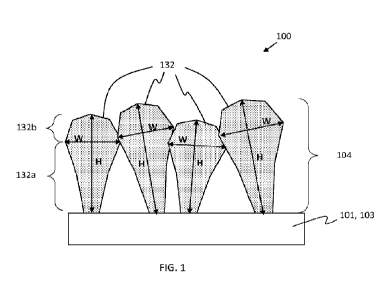
FIG.1 is a cross-sectional view of an anode according to some embodiments of
the
present disclosure. Anode 100 includes a current collector 101 having an
electrically
conductive layer 103 and a lithium storage structure 104 over the electrically
conductive
layer. Lithium storage structure includes a plurality of first microstructures
132 formed in
contact with the electrically conductive layer. The first microstructures
include a lithium
3
CA 03172496 2022- 9- 20
WO 2021/207357
PCT/US2021/026179
storage material capable of reversibly incorporating lithium. In some
embodiments, the first
microstructures may include a porous material. In some embodiments, the first
microstructures may include silicon, germanium, tin, antimony, or a
combination thereof In
some embodiments, the first microstructures contain at least 50 atomic %
silicon, alternatively
at least 60%, alternatively at least 70%, alternatively at least 80%,
alternatively at least 90%.
Each first microstructure is characterized by a first maximum width W measured
across the widest section orthogonal to the first microstructure axis, and by
a first height H
measured from the electrically conductive layer to its end along the first
microstructure axis.
The first microstructure axis is the longitudinal axis of the first
microstructure. The first
microstructure axis may pass through the center of mass of the first
microstructure. Each first
microstructure includes a first portion 132a characterized by the width
substantially tapering
from the maximum width to a location where it contacts the electrically
conductive layer.
Each first microstructure also includes a second portion 132b, the second
portion positioned
farther away from the electrically conductive layer than the first portion is
from the
electrically conductive layer, the second portion defining a substantially
hemispherical shape
and the top of each first microstructure.
The term "substantially hemispherical shape" encompasses a broad number of
structures. FIGS. 2 and 3 illustrate just a few substantially hemispherical
shapes contemplated
by the present disclosure which may correspond to second portion 132b. FIGS.
2A ¨ 2F
illustrate various non-limiting cross-sectional views of second portion 132b
and FIGS. 3A ¨
3L shows various, non-limiting top views of second portion 132b. As shown in
FIG 2, in
some embodiments, a substantially hemispherical shape may have a smoothly
rounded
surface, a faceted surface structure, a conical surface, or an irregular
surface. As shown in
FIG. 3, the top view shape of the second portion 132b may appear circular,
oval, oblong,
polygonal, or irregular, and may be matched to any of the cross-sectional
views of FIG. 2.
Substantially hemispherical shapes may be characterized by a cross-sectional
area through the
maximum width. The cross-sectional area may taper to a smaller area along the
first height.
The minimum cross-sectional area of the substantially hemispherical shape may
be at the
maximum value of the first height.
In some embodiments, the first microstructures have a first height of at least
9 p.m and
a first maximum width of at least 4.5 jam. In some embodiments the first
microstructures have
4
CA 03172496 2022- 9- 20
WO 2021/207357
PCT/US2021/026179
a first height in a range of 9 gm to 15 gm, alternatively 15 gm to 20 urn,
alternatively, 20 gm
to 25 gm, alternatively 25 gm to 30 p,m, alternatively 30 gm to 35 gm,
alternatively 35 urn to
40 gm, alternatively 40 gm to 50 gm, alternatively 50 gm to 60 gm or an
combination of
contiguous ranges thereof. In some embodiments, the first microstructures have
a first
maximum width in a range of 4.5 gm to 6 gm, alternatively 6 gm to 8 gm,
alternatively, 8 gm
to 10 gm, alternatively 10 gm to 12 gm, alternatively 12 gm to 14 gm,
alternatively 14 g.m to
16 gm, or any combination of contiguous ranges thereof The first
microstructures each have
an aspect ratio defined as the first height divided by the first maximum
width. In some
embodiments, the first microstructures have a first aspect ratio in a range of
1.4 to 1.6,
alternatively 1.6 to 1 8, alternatively 1 8 to 2.0, alternatively 2.0 to 2.5,
alternatively 2.5 to
3.0, alternatively 3.0 to 3.5, alternatively 3.5 to 4.0, or any combination of
contiguous ranges
thereof The height, maximum width and aspect ratio described herein may
represent the
mean average, median, or mode of the first microstructures.
Unlike nanowires of the prior art, which are mostly spaced apart and have
aspect ratios
of greater than 4, the first microstructures of the present disclosure are
tightly packed, i.e.,
spaced very close to one another and often in contact. In some embodiments, at
least 50%,
alternatively at least 70%, alternatively at least 80%, alternatively at least
90%, alternatively
substantially all of the first microstructures are in contact with at least
one other first
microstructure, alternatively at least two other first microstructures.
Despite prior art
suggestions to avoid tight packing of lithium storage structures to allow for
expansion during
lithiation, it has been unexpectedly found that first microstructures
according to various
embodiments of the present disclosure may provide anodes having high charge
capacity and
cycle stability even at high charge rates such as 3C.
Anodes of the present disclosure may further comprise second microstructures
that are
substantially different than the first microstructures. As shown in FIG. 4,
anode 180 is similar
to anode 100 except that lithium storage structure 104 further includes one or
more second
microstructures 182 in contact with the electrically conductive layer. In some
embodiments,
the second microstructures may include silicon. Although not explicitly shown
in FIG. 4, the
second microstructures can be characterized in a manner analogous to the first
microstructures
as having a second height and a second maximum width. In some embodiments, the
second
microstructures are shorter than the first microstructures, i.e., they have a
second height that is
5
CA 03172496 2022- 9- 20
WO 2021/207357
PCT/US2021/026179
less than the first height of the first microstructures, as exemplified in
second microstructures
182a and 182b. In some embodiments, the second microstructures are not as wide
as the first
microstructures, i.e., they have a second maximum width less than the first
maximum width
of the first microstructures, as exemplified in second microstructures 182a,
182b, and 182c. In
some embodiments, the second microstructures are characterized by a second
aspect ratio that
is greater than the first aspect ratio microstructures, as exemplified in
second microstructures
182b and 182c. The second microstructures may include nanopillars or nanowires
(e.g., 182b
and 182c) or the second microstructures may be smaller versions of the first
microstructures
(e.g., 182a).
The second microstructures may have some lithium storage capacity, but in some
embodiments, the first microstructures account for at least 50% of the lithium
storage capacity
of the anode, alternatively at least 80%, alternatively at least 90%.
Electrically Conductive Layer / Current Collector
In some embodiments, the electrically conductive layer includes a metallic
material,
e.g., nickel (and its alloys), copper (and its alloys), or stainless steel. In
some embodiments,
the electrically conductive layer includes an electrically conductive carbon,
such as carbon
black, graphene, graphene oxide, graphite, carbon nanotubes, or fullerene. In
some
embodiments the electrically conductive layer may have a conductivity of at
least 1 S/m, 103
S/m, or alternatively at least 106 S/m, or alternatively at least 107 S/m, and
may include
inorganic or organic conductive materials, or a combination thereof
The current collector may be a continuous foil or sheet but may alternatively
be a wire
mesh, have a fabric-like structure or have some other 3-dimensional structure.
In some
embodiments, the current collector 101 and the electrically conductive layer
103 may be one
and the same, for example, when the current collector has substantially a
single composition
and does not have a multilayered structure. Such embodiment is shown in FIG. 1
and FIG. 4.
Referring to FIG. 5, in some embodiments, a lithium storage structure 104-1
having first
microstructures 132-1 is provided over a first side 103-1 of the electrically
conductive layer
103, and another lithium storage structures 104-2 having first microstructures
132-2 is
provided on a second side 103-2 of the electrically conductive layer 103. In
some
embodiments, the first microstructures 103-1 of lithium storage structure 104-
1 are
substantially the same as the first microstructures 103-2 of lithium storage
structure 104-2
6
CA 03172496 2022- 9- 20
WO 2021/207357
PCT/US2021/026179
with respect to structural dimensions, chemical composition, or both. In some
embodiments,
the first microstructures 103-1 may differ from first microstructures 103-2
with respect to
structural dimensions, e.g., by more than 100/c with respect to height,
maximum width, or
aspect ratio, to chemical composition, e.g., the relative elemental
composition differs by at
least 10% with respect to at least one element present in at least 0.1 atomic
%, or both.
Alternatively, one side may include second microstructures and the other side
may not include
such second microstructures, or the second microstructures are different.
Alternatively, one
side may not include any first microstructures and instead include a
substantially different
type of lithium storage layer or material (e.g., a continuous layer or high
aspect ratio
nanostructures) In some embodiments, one side may include a lithium storage
layer as
disclosed in U.S. Patent Application No. 16/285842 which is herein
incorporated by reference
for all purposes.
In the case where the current collector or electrically conductive layer take
the form of
a wire mesh or fabric, the lithium storage structure may be provided over the
entire mesh or
fabric, e.g., as shown in FIG. 6 that illustrates a cross-section of the mesh
or fabric "wire"
which acts as the electrically conductive layer. FIG. 6 shows the lithium
storage structure
having first microstructures 232 provided in an approximately conformal manner
around the
electrically conductive layer wire 203, but in other embodiments the lithium
storage structure
may be provided non-conformally or only a portion of the mesh wires.
In some embodiments, as shown in cross-section in FIG. 7, the current
collector 301
may have a multilayered structure including electrically conductive layers
103a and 103b
provided on either side of additional layer 102 that is spaced away from the
lithium storage
structures 104-1 and 104-2 and their corresponding plurality of first
microstructures 132-1
and 132-2. Electrically conductive layers 103a and 103b may be the same or
different, e.g.,
with respect to chemical composition or thickness. As described with respect
to FIG. 5 above,
first microstructures 132-1 may be the same as or different from first
microstructures 132-2.
Layer 102 may be electrically insulating, semiconducting or conducting. In
some
embodiments, layer 102 is an electrically conductive metal or carbon, such as
described above
with respect to electrically conductive layer. Multilayer current collector
301 may be in the
form of a foil or sheet but may alternatively be a wire mesh, have a fabric-
like structure or
have some other 3-dimensional structure. In some embodiments, layer 102 may
include
7
CA 03172496 2022- 9- 20
WO 2021/207357
PCT/US2021/026179
stainless steel or conductive carbon and electrically conductive layer 103a or
103b or both
include nickel or copper. In some embodiments, layer 102 may include copper
and electrically
conductive layers 103a and 103b include nickel. In some embodiments when layer
102 is
electrically insulating, the voltage or current applied to conductive layer
103a may be
controlled separately from conductive layer 103b. Alternatively, when layer
102 is electrically
insulating, electrically conductive layers 103a and 103b may be shorted
together elsewhere in
the structure (not shown) to allow a common voltage or current.
Formation of first microstructures
Methods of forming first microstructures in contact with the electrically
conductive
layer may include a chemical vapor deposition (CVD) method. Such methods are
generally
known for forming high aspect ratio nanowires, e.g., as described in US9325014
and
US8257866, the entire contents of which are incorporated by reference for all
purposes, but
such methods may be modified to form tightly packed first microstructures of
the present
disclosure
CVD generally involves flowing a precursor gas, a gasified liquid in terms of
direct
liquid injection CVD or gases and liquids into a chamber containing one or
more objects,
typically heated, to be coated. Chemical reactions occur on and near the hot
surfaces, resulting
in the deposition of a thin film on the surface. This is accompanied by the
production of
chemical by-products that are exhausted out of the chamber along with
unreacted precursor
gases. As would be expected with the large variety of materials deposited and
the wide range
of applications, there are various types of CVD that may be used to form the
lithium storage
structures, a supplemental layer (see below) or other layers. It may be done
in hot-wall
reactors or cold-wall reactors, at sub-ton total pressures to above-
atmospheric pressures, with
or without carrier gases, and at temperatures ranging from 100-1600 C in some
embodiments.
There are also a variety of enhanced CVD processes, which involve the use of
plasmas, ions,
photons, lasers, hot filaments, or combustion reactions to increase deposition
rates and/or
lower deposition temperatures. Various process conditions may be used to
control the
deposition, including but not limited to, temperature, precursor material, gas
flow rate,
pressure, substrate voltage bias (if applicable), and plasma energy (if
applicable).
As described below, the lithium storage structures, e.g., those containing
silicon,
germanium, tin, or a combination, may be provided in part or entirely by
plasma-enhanced
8
CA 03172496 2022- 9- 20
WO 2021/207357
PCT/US2021/026179
chemical vapor deposition (PECVD). Relative to thermal CVD, deposition by
PECVD can
often be done at lower temperatures and higher rates, which can be
advantageous for higher
manufacturing throughput. hi some embodiments, the PECVD may be used to
deposit a
substantially amorphous silicon material that may optionally be doped.
In PECVD processes, according to various implementations, a plasma may be
generated in a chamber in which the substrate is disposed or upstream of the
chamber and fed
into the chamber. Various types of plasmas may be used including, but not
limited to,
capacitively-coupled plasmas, inductively-coupled plasmas, and conductive
coupled plasmas.
Any appropriate plasma source may be used, including DC, AC, RF, VI-1T',
combinatorial
PECVD and microwave sources may be used
PECVD process conditions (temperatures, pressures, precursor gases, carrier
gasses,
dopant gases, flow rates, energies and the like) can vary according to the
particular process
and tool used, as is well known in the art.
In some implementations, the PECVD process is an expanding thermal plasma
chemical vapor deposition (ETP-PECVD) process. In such a process, a plasma
generating gas
is passed through a direct current arc plasma generator to form a plasma, with
a web or other
substrate including the current collector optionally in an adjoining vacuum
chamber. A silicon
source gas is injected into the plasma, with radicals generated. The plasma is
expanded via a
diverging nozzle and injected into the vacuum chamber and toward the
substrate. An example
of a plasma generating gas is argon (Ar). In some embodiments, the ionized
argon species in
the plasma collide with silicon source molecules to form radical species of
the silicon source,
resulting in deposition onto the current collector. Example ranges for
voltages and currents for
the DC plasma source are 60 to 80 volts and 40 to 70 amperes, respectively.
Any appropriate silicon source may be used to deposit silicon, including
silane (SiH4),
dichlorosilane (H2SiC12), monochlorosilane (H3SiC1), trichlorosilane (HSiC13),
silicon
tetrachloride (SiC14), and diethylsilane. Depending on the gas(es) used, the
silicon layer may
be formed by decomposition or reaction with another compound, such as by
hydrogen
reduction. In some embodiments, the gases may include a silicon source such as
silane, a
noble gas such as helium, argon, neon or xenon, optionally one or more dopant
gases, and
substantially no hydrogen. In some embodiments, the gases may include argon,
silane, and
hydrogen, and optionally some dopant gases. In some embodiments when forming
first
9
CA 03172496 2022- 9- 20
WO 2021/207357
PCT/US2021/026179
microstructures, the gas flow ratio of argon relative to the combined gas
flows for silane and
hydrogen is at least 3.0, alternatively at least 4Ø In some embodiments, the
gas flow ratio of
argon relative to the combined gas flows for silane and hydrogen is in a range
of 3.0 to 10,
alternatively 4.0 to 8Ø In some embodiments, the gas flow ratio of silane
relative to the
combined gas flows of silane and hydrogen is in a range of 0.20 to 0.95,
alternatively 0.30 to
080, alternatively 040 to 0.70.
In some embodiments, at least the surface of electrically conductive layer 103
includes
a filament growth catalyst material. A filament growth catalyst material may
assist in
initiating and growing the first microstructures, at least at first. For the
purposes of this
disclosure, filament growth catalyst materials include "true" catalytic
materials that remain
active indefinitely, and materials that may eventually be consumed during
filament growth. In
some embodiments the filament growth catalyst material may be a vapor-liquid-
solid (VLS)
filament growth catalyst material. In some embodiments the filament growth
catalyst material
may be provided as a substantially continuous layer that corresponds to
electrically
conductive layer 103. In some embodiments, the electrically conductive layer
103 may
include a pattern of filament growth catalyst material where the pattern may
be random or
predetermined. In some embodiments the electrically conductive layer may be a
metal foil
that is itself a filament growth catalyst material, for example, nickel. Non-
limiting examples
of catalyst materials may include non-refractory transition metals and their
alloys. The
catalyst material may include, for example, nickel, gold, palladium, platinum,
ruthenium,
aluminum, indium, gallium, tin, or iron, or their alloys
Referring to FIG. 8A, in some embodiments, forming first microstructures may
include growing a plurality of base filaments 120 on the electrically
conductive layer. In some
embodiments this is done by VLS method whereby the current collector is
exposed to a
filament precursor gas under elevated temperatures. The temperature depends on
the catalyst
and filament precursor gas, but in some embodiments may be at least 300 C,
alternatively at
least 400 C, alternatively at least 500 C, alternatively at least 600 C. In
some
embodiments, the temperature is in a range of 300 C to 400 C, alternatively
400 C to 500
C, alternatively 500 C to 600 C, or any combinations of contiguous ranges
thereof. In some
embodiments, the filament precursor gas is a silicon-containing gas such as
silane or a
germanium-containing gas such as germane, but alternative silicon- and
germanium-
CA 03172496 2022- 9- 20
WO 2021/207357
PCT/US2021/026179
containing gases may be used. In some embodiments, the filaments include a
silicide or
germanium alloy. The base filaments may be electrically conductive or semi-
conductive. In
some embodiments the filament growth catalyst material may include nickel and
the base
filaments include nickel silicide. In some embodiments, the filament growth
catalyst material
may be consumed during formation of the base filaments.
As shown in FIG. 8B, in some embodiments, a plurality of first microstructures
132
may be formed by depositing a lithium storage material 121 over the base
filament 120.
Lithium storage material 121 may have a different chemical composition than
base filament
120. In some embodiments, the lithium storage material may include silicon,
germanium, tin,
or a combination thereof. In some embodiments, the first microstructures are
formed at least
in part by some type of a CVD (chemical vapor deposition) process, such as
Thermal CVD,
HVVCVD (hot-wire CVD), and/or PECVD (plasma enhanced chemical vapor
deposition). In
some embodiments, base filaments 120 may be grown by a thermal CVD process and
lithium
storage material may be deposited by HWCVD or PECVD. In some embodiments, base
filaments 120 may be grown by PECVD and the lithium storage material 121 may
also be
deposited by PECVD. The vapor deposition process may include a lithium storage
precursor
gas that contains silicon (e.g., silane), germanium (e.g., germane), or tin
(e.g., Sn(IV) tert-
butoxide). In some embodiments, base filaments 120 may be grown in a separate
step or
chamber than lithium storage material 121 deposition. In some embodiments,
base filaments
120 may be grown in the same chamber as used for depositing lithium storage
material 121.
In some embodiments, the growth of base filaments and formation of first
microstructures 132
may be performed in a common step without substantially changing conditions,
e.g., by using
a catalyst that is consumed, such that base filament formation stops and
deposition of lithium
storage material 121 begins. That is, the base filament formation may be self-
limiting.
Alternatively, conditions are altered after base filament growth (temperature,
precursor gas,
gas pressure, carrier or other gasses, plasma power, deposition angle, or the
like) to promote
deposition of lithium storage material 121 and formation of the first
microstructures 132.
Although FIG. 8B shows a discrete base filament, in some embodiments, no base
filament is
present. For example, there may be gradual transition between initial base
filament formation
and lithium storage material deposition. In some embodiments, the first
microstructures may
include a metal silicide base filament 120 (e.g. a nickel silicide or copper
silicide) and a
11
CA 03172496 2022- 9- 20
WO 2021/207357
PCT/US2021/026179
silicon-containing lithium storage material 121 that may also contain some of
the metal but at
a lower atomic % than the base filament portion. That is, the lithium storage
material 121 may
have a higher atomic % silicon than the base filament 120 In some embodiments,
there is a
gradient in metal silicide content with highest levels near the electrically
conductive layer and
lowest levels at the opposite end of the first microstructure. In some
embodiments, the base
filament portion of the first microstructures may have some lithium storage
capacity, but
lower than the lithium storage capacity of the lithium storage material
portion in terms of
mAh/g.
In some embodiments, the first microstnictures 132 (or the lithium storage
material
121) include substantially amorphous silicon. Such substantially amorphous
silicon may
include some, e.g., less than 20 atomic %, crystalline silicon (not including
any silicides)
which may be dispersed therein. The first microstructures 132 (or the lithium
storage material
121) may include dopants such as hydrogen, boron, nitrogen, phosphorous,
sulfur, fluorine,
aluminum, gallium, indium, arsenic, antimony, bismuth, or other metallic
elements. In some
embodiments the first microstructures 132 (or the lithium storage material
121) may include
substantially amorphous hydrogenated silicon (a-Si:H), having, e.g., a
hydrogen content of
from 0.1 to 20 atomic %, or alternatively higher. In some embodiments, the
first
microstructures 132 (or the lithium storage material 121) may include
methylated amorphous
silicon.
In some embodiments, the first microstructures 132 (or lithium storage
material 121)
are porous, i e , they include some pores 170 as shown in FIG 9 The pores may
be void
spaces or may be occupied by a gas. In some embodiments, the pores have a
maximum
dimension of less than 3 um, alternatively less than 2 um. In some
embodiments, the porosity
of the first microstructures 132 (or lithium storage material 121), i.e., the
volume percent of
pores relative to the total volume, is at least 0.1%, alternatively at least
0.5%, alternatively at
least 1%, alternatively at least 2 %, alternatively at least 5%. In some
embodiments, the
porosity of the first microstructures 132 (or lithium storage material 121) is
less than 50%,
alternatively less than 40%, alternatively less than 25%. The porosity of the
first
microstructures 132 or lithium storage material 121 may be in a range of 0.1%
to 0.5%,
alternatively 0.5% to 1%, alternatively 1% to 2 ,43, alternatively 2% to 5%,
alternatively 5% to
10%, alternatively 10% to 15%, alternatively 15% to 20%, alternatively 20% to
25%,
12
CA 03172496 2022- 9- 20
WO 2021/207357
PCT/US2021/026179
alternatively 25% to 30%, alternatively 30% to 40%, alternatively 40% to 50%,
or any
combination of contiguous ranges thereof. Pore sizes may be polydisperse or
monodisperse
and distributed in a random or uniform manner.
In some embodiments, the lithium storage structure may be characterized as
having an
active silicon areal density of at least 1 mg/cm2, alternatively at least 2
mg/cm2, alternatively
at least 3 mg/cm2, alternatively at least 5 mg/cm2. In some embodiments, the
lithium storage
structure may be characterized as having an active silicon areal density in a
range of 1 ¨ 2
mg/cm2, alternatively in a range of 2 ¨ 3 mg/cm2, alternatively in a range of
3 ¨ 5 mg/cm2,
alternatively in a range of S ¨ 10 mg/cm2, alternatively in a range of 10¨ 15
mg/cm2,
alternatively in a range of 15 ¨ 20 mg/cm2, or any combination of contiguous
ranges thereof.
"Active silicon" refers to the silicon in electrical communication with the
current collector
that is available for reversible lithium storage at the beginning of cell
cycling, e.g., after anode
"electrochemical formation" discussed later. "Areal density" refers to the
surface area of the
electrically conductive layer over which active silicon is provided. In some
embodiments, not
all of the silicon content is active silicon, i.e., some may be tied up in the
form of non-active
silicides or electrically isolated from the current collector.
In some embodiments, the electrically conductive layer includes nickel or
copper, the
lithium storage structure includes at least 1.1 mg/cm2 of active silicon, and
when analyzed by
energy dispersive x-ray spectroscopy (EDS) the lithium storage structure is
characterized as
having a total atomic % of nickel and copper of less than 1.2%, alternatively
less than 1.0%,
alternatively less than 0.9%, alternatively less than 0.S%, alternatively less
than 0.7%. A
typical EDS compositional analysis may be performed using a scanning electron
microscope
(SEM), for example, a Tescan Mira3 SEM, equipped with an energy dispersive
spectrometer,
e.g., from Broker, operating at 20kV. Measurements may be made at a working
distance of
about 10 mm from the sample surface, and on a sample area of at least 1600
p.m', for
example, 40 um x 40 gm regions at 5000x magnification. The EDS measurement
defined
above may not necessarily be a measurement of the total amount of nickel or
copper in the
entire lithium storage structure, but it has been found to be a useful metric
that relates to the
structure of the lithium storage structure. While EDS may be able to probe
several microns
into a surface, there can be a falloff in sensitivity such that elements
nearer the surface may
dominate the analysis over elements far down into the layer. A portion of the
lithium storage
13
CA 03172496 2022- 9- 20
WO 2021/207357
PCT/US2021/026179
structure including the surface of the lithium storage structure may have a
total atomic % of
nickel and copper of less than 1.2%, alternatively less than 1.0%,
alternatively less than 0.9%,
alternatively less than 0.8%, alternatively less than 0.7%. In some
embodiments, a portion of
the lithium storage structure including the surface of the lithium storage
structure may have a
total atomic % of nickel and copper of at least 0.05%, alternatively at least
0.1%. In some
embodiments, a portion of the lithium storage structure including the surface
of the lithium
storage structure may have a total atomic % of nickel and copper in a range of
0.05% to 0.1%,
alternatively 0.1% to 0.2%, alternatively 0.2% to 0.3%, alternatively 0.3% to
0.4%,
alternatively 0.4% to 0.5%, alternatively 0.5% to 0.6%, alternatively 0.6% to
0.7%,
alternatively 0.7% to 0.8%, alternatively 0.8% to 0.9%, alternatively 0.9% to
1.0%,
alternatively 1.0% to 1.1%, alternatively 1.1% to less than 1.2%. The portion
of the lithium
storage structure may include the upper 1 gm, 2 gm, 3 gm, 4 gm, or 5 gm of the
lithium
storage structure. In general, first microstructures having taller height are
found by this
method to have lower atomic % nickel and copper. This may be due in part to
higher metal
silicide concentration closer to the electrically conductive layer than at the
surface. Further,
first microstructure having tighter packing are found by this method to have
lower atomic %
nickel and copper. This may be due in part to the crowded nature of the first
microstructures
causing more blocking EDS sampling of the underlying nickel or copper
electrically
conductive layer. Spaced apart nanowires of the prior art, on the other hand,
may permit more
EDS sampling of the underlying nickel or copper electrically conductive layer.
In some embodiments, the lithium storage stnicture may be characterized as
having a
total reflectance of at least 10% measured at 550 nm, alternatively at least
15%, alternatively
at least 20%. Unlike prior art nanowire structures which trap light and appear
dark or black,
some embodiments of anodes of the present disclosure have higher reflectivity
due in part to
the tightly packed first microstructures that have less apparent roughness
than nanowires and
may prevent light trapping.
Compared to prior art nanowires that easily rub off of the current collector,
some
embodiments of lithium storage structures of the present disclosure are
physically more robust
to abrasion, handling and other battery assembly operations. This may be due
in part to their
smoother surface and/or the collective structural support provided by the
tight packing of first
microstructures.
14
CA 03172496 2022- 9- 20
WO 2021/207357
PCT/US2021/026179
Supplemental Layers
In some embodiments, the anode may further include one or more supplemental
layers
provided over the lithium storage structure. As shown in FIG. 10A,
supplemental layer 150
may be provided primarily over the top portion of the lithium storage
structure 104 or first
microstructures 132, e.g., primarily over the second portion 132b (referring
again to FIG. 1).
In some embodiments, as shown in FIG. 10B, supplemental layer 150 may also be
provided
over more or all of the first microstructures, including some or all of the
first portion 132a
(referring again to FIG. 1). The degree to which supplemental layer material
is provided over
first portions 132a of the first microstn.ictures may depend on the packing
density of the first
microstructures and the coating method. For example, ALD coating methods may
be more
conformal than some CVD or physical vapor deposition methods. In some
embodiments,
supplemental layer 150 may include silicon nitride or a metal compound as
described below.
In some embodiments, as shown in FIG 11, the anode may include a first
supplemental layer 150-1 and a second supplemental layer 150-2. FIG. 11
illustrates an
embodiment where the first and second supplemental layers are provided
primarily over the
top portion of the first microstructures, but in some embodiments, one or both
supplemental
layers are further provided over more or all of the first microstructures in a
manner similar to
that shown in FIG. 10B. In some embodiments, the first supplemental layer 150-
1 may
include silicon nitride or a first metal compound. The second supplemental
layer 150-2 has a
composition different from the first supplemental layer and may include
silicon nitride or a
second metal compound
In some embodiments, the first supplemental layer 150-1 and the optional
second or
additional supplemental layers may help stabilize the lithium storage
structure by providing a
barrier to direct electrochemical reactions with solvents or electrolytes that
can degrade the
interface. The supplemental layer(s) are generally conductive to lithium ions
and permit
lithium ions to move into and out of the lithium storage structures during
charging and
discharging. In some embodiments, the lithium ion conductivity of each
supplemental layer
may be at least 10'9 S/cm, alternatively at least 10-8 S/cm, alternatively at
least 10 S/cm, or
alternatively at least 10-6 S/cm. In some embodiments, the supplemental layer
may function in
part as a solid-state electrolyte. In some embodiments, the supplemental
layer(s) are less
electrically conductive than the lithium storage structure so that little or
no electrochemical
CA 03172496 2022- 9- 20
WO 2021/207357
PCT/US2021/026179
reduction of lithium ions to lithium (0) occurs at the supplemental
layer/electrolyte interface.
In addition to providing protection from electrochemical reactions, the
multiple supplemental
layer structure embodiments may provide superior structural support. In some
embodiments,
although the supplemental layers may flex and may form fissures when the first
microstructures expand during lithiation, crack propagation can be distributed
between the
layers to reduce direct exposure of the lithium storage structure to the bulk
electrolyte. For
example, a fissure in the second supplemental layer may not align with a
fissure in the second
supplemental layer. Such an advantage may not occur if just one thick
supplemental layer is
used. In an embodiment, the second supplemental layer may be formed of a
material having
higher flexibility than the first supplemental layer.
In some embodiments, a supplemental layer (the first supplemental layer, the
second
supplemental layer, or any additional supplemental layer(s)), may include
silicon nitride, e.g.,
substantially stoichiometric silicon nitride where the ratio of nitrogen to
silicon is about 1.33,
alternatively in a range of 1.33 to 1.25. A supplemental layer comprising
silicon nitride may
have a thickness in a range of about 0.5 nm to about 50 nm, alternatively
about 5 nm to about
40 nm, alternatively 1 nm to 10 nm, alternatively 10 nm to 20 nm,
alternatively 20 nm to 30
nm, alternatively 30 nm to 40 nm, alternatively 40 nm to 50 nm, or any
combination of
contiguous ranges thereof Silicon nitride may be deposited by an atomic layer
deposition
(ALD) process or by a CVD process. In some embodiments, the lithium storage
filamentary
structures include silicon deposited by some type of CVD process as described
above, and at
the end, a nitrogen gas source is added to the CVD deposition chamber along
with the silicon
source.
In some embodiments a supplemental layer (the first supplemental layer, the
second
supplemental layer, or any additional supplemental layer(s)) may include a
metal compound.
In some embodiments, the metal compound may include is a metal oxide, metal
nitride, or
metal oxynitride, e.g., those containing a transition metal, aluminum,
titanium, vanadium,
zirconium, germanium or tin, or mixtures thereof. In some embodiments a metal
oxide or
metal oxynitride may include some corresponding metal hydroxide. In some
embodiments, a
supplemental layer including a simple metal oxide, metal nitride, or metal
oxynitride, may
have an average thickness of less than about 100 nm, for example, in a range
of about 0.5 nm
to about 50 nm, or alternatively in a range of about 5 nm to about 40 nm,
alternatively 1 nm to
16
CA 03172496 2022- 9- 20
WO 2021/207357
PCT/US2021/026179
nm, alternatively 10 nm to 20 nm, alternatively 20 nm to 30 nm, alternatively
30 nm to 40
nm, alternatively 40 nm to 50 nm. The metal oxide, metal nitride, or metal
oxynitride may
include other components or dopants such as phosphorous or silicon.
In some embodiments, the metal compound may include a lithium-containing
material
5 such as lithium phosphorous oxynitride (LIPON), a lithium phosphate, a
lithium aluminum
oxide, or a lithium lanthanum titanate. In some embodiments, the thickness of
supplemental
layer including a lithium-containing material may be in a range of 0.5 nm to
200 nm,
alternatively 1 nm to 10 nm, alternatively 10 nm to 20 nm, alternatively 20 nm
to 30 nm,
alternatively 30 nm to 40 nm, alternatively 40 nm to 50 nm, alternatively 50
nm to 100 nm,
10 alternatively 100 to 200 nm, or any combination of contiguous ranges
thereof.
In some embodiments the metal compound may be deposited by a process
comprising
ALD, thermal evaporation, sputtering, or e-beam evaporation ALD is a thin-film
deposition
technique typically based on the sequential use of a gas phase chemical
process. The majority
of ALD reactions use at least two chemicals, typically referred to as
precursors. These
precursors react with the surface of a material one at a time in a sequential,
self-limiting,
manner. Through the repeated exposure to separate precursors, a thin film is
deposited, often
in a conformal manner. In addition to conventional ALD systems, so-called
spatial ALD
(SALD) methods and materials can be used, e.g., as described U.S. Patent No.
7,413,982, the
entire contents of which are incorporated by reference herein for all
purposes. In certain
embodiments, SALD can be performed under ambient conditions and pressures and
have
higher throughput than conventional ALD systems
In some embodiments, the process for depositing the metal compound may include
electroless deposition, contact with a solution, contact with a reactive gas,
or electrochemical
methods. In some embodiments, a metal compound may be formed by depositing a
metallic
layer (including but not limited to thermal evaporation, CVD, sputtering, e-
beam evaporation,
electrochemical deposition, or electroless deposition) followed by treatment
to convert the
metal to the metal compound (including but not limited to, contact with a
reactive solution,
contact with an oxidizing agent, contact with a reactive gas, or a thermal
treatment).
In some embodiments, the metal compound may include an organic material bound
to
a metal or to a metal oxide. In some embodiments, a supplemental layer may
include an
inorganic-organic hybrid structure having alternating sublayers of metal oxide
and bridging
17
CA 03172496 2022- 9- 20
WO 2021/207357
PCT/US2021/026179
organic materials such as so-called "metalcone materials (and which are herein
included as a
type of metal compound that may be suitable for one or more supplemental
layers). In some
embodiments, a supplemental layer that includes a metalcone may provide
improved
flexibility to accommodate volume changes in the lithium-storage material
during lithiation
and de-lithiation. Metalcones may be made using a combination of atomic layer
deposition to
apply the metal oxide and molecular layer deposition (MLD) to apply the
organic. This may
also form a coating that is largely conformal due to the self-limiting nature
of the reactions.
The organic bridge is typically a molecule having multiple functional groups.
One group can
react with a sublayer comprising a metal oxide and the other group is
available to react in a
subsequent ALD step to bind a new metal. The process is shown schematically in
FIGS. 12A
¨ 12C wherein the metal is aluminum and the reactive organic functional groups
are hydroxy
groups of glycerol. There is a wide range of reactive organic functional
groups that may be
used including, but not limited to hydroxy, carboxylic acid, amines, acid
chlorides and
anhydrides. Although not shown, the structure in FIG. 12C may be treated again
with glycerol
or some other reactive organic material to react with aluminum and release
methane.
Alternatively, the methyl-aluminum bonds of FIG. 12C may be oxidized with an
oxygen
source. In any event, the cycle can continue to optionally form numerous
alternating
sublayers, which can end with either application of the reactive organic
material (i.e., the final
organic layer is not functioning as a bridge to another metal layer) or with
the metal-
containing material. Components of the sublayers can be varied between cycles.
For the
purposes of the present disclosure, this alternating sublayer structure is
considered a single
supplemental layer. Almost any metal precursor suitable for ALD deposition can
be used.
Some non-limiting examples include ALD compounds for aluminum (e.g., trimethyl
aluminum), titanium (e.g., titanium tetrachloride), zinc (e.g., diethyl zinc),
and zirconium
(tris(dimethylamino)cyclopentadienyl zirconium). As mentioned, the
supplemental layers
should allow transport of lithium ions. In some embodiments, the organic
bridging materials
may include additional functional groups that are not involved in layer
binding but help
facilitate such transport. In an embodiment, these additional functional
groups are oxygen-
containing, such as (unreacted) hydroxy or ether groups. The organic bridging
material may
include aliphatic, aromatic, heteroaromatic or a combination of carbon
structures. The organic
bridging material may include cross-linkable groups such as epoxy groups,
double bonds or
18
CA 03172496 2022- 9- 20
WO 2021/207357
PCT/US2021/026179
triple bonds that can be thermally, chemically or photo cross-linked after
deposition. The
alternating organic-inorganic sublayers within the supplemental layer is not
limited to a single
set. Different organic materials and inorganic compounds may be used to form
the inorganic-
organic hybrid supplemental layer. In some embodiments, a supplemental layer
having a
structure of alternating inorganic-organic hybrid sublayers may have a
thickness in a range of
0.5 nm to 200 nm, alternatively 1 nm to 10 nm, alternatively 10 nm to 20 nm,
alternatively 20
nm to 30 nm, alternatively 30 nm to 40 nm, alternatively 40 nm to 50 nm,
alternatively 50 nm
to 100 nm, alternatively 100 to 200 nm, or any combination of contiguous
ranges thereof.
Organic Material Capping Layer
In some embodiments as shown in FIG. 13, the anode may include an organic
material
capping layer 160 attached (e.g., adsorbed or bonded) to the lithium storage
structure or
outermost supplemental layer, in this example, the second supplemental layer
150-2. The
outermost supplemental layer may be the supplemental layer disposed farthest
from the
electrically conductive layer. Additionally, the outermost supplemental layer
may be the
supplemental layer with the largest average or median distance from the
electrically
conductive layer.
Unlike metalcones, the organic material capping layer of this disclosure does
not have
an alternating structure of inorganic/organic sublayers. In some embodiments,
the organic
material capping layer may be provided in part via a chemical reaction between
a reactive
functional group of an organic material and a supplemental layer having a
correspondingly
reactive surface In some embodiments, the organic material capping layer may
be a
monolayer. In some embodiments, the organic material capping layer may be
formed over an
outermost supplemental layer containing a metal compound. In some embodiments,
the
organic material capping layer is formed over an outermost supplemental layer
containing a
metal oxide. In some embodiments, chemistry similar to that described above
with respect to
metalcones may be used where organic compounds have appropriate reactive
groups such as
hydroxy, carboxylic acid, amines and anhydrides, capable of reacting with
metal bonds of an
outermost supplemental layer (e.g., metal-carbon or metal-halogen). In some
embodiments,
the outermost supplemental layer may not initially include metal-carbon or
metal-halogen
bonds, but its surface may be modified to include such bonds prior to treating
with the
19
CA 03172496 2022- 9- 20
WO 2021/207357
PCT/US2021/026179
reactive organic compound. As with supplemental layers, the capping layer
should also be
conductive to lithium ion diffusion.
Alternatively, rather than reacting with metal-carbon or metal-halogen bonds,
some
organic materials may react with, or chemisorb to, a metal oxide- or metal
hydroxide-
containing outermost supplemental layer, e.g., aluminum oxide or titanium
oxide. Such
organic materials may include appropriate functional groups such as hydroxyl,
carboxylic
acid, amines, amino acid, esters, ethers, acid chlorides or anhydrides to aid
in the reaction or
chemisorption. The organic compounds forming the organic material capping
layer may
include small molecules, large molecules or polymers so long as they have
appropriate
reactive groups Depending on the particular properties of the chemical, the
organic
compound may be applied by vapor deposition, from a solution in an inert
solvent or as a neat
liquid. The organic materials may include additional functional groups that
are not involved in
layer binding that help facilitate transport of lithium ions. In some
embodiments, these
additional functional groups are oxygen-containing, such as hydroxy or ether
groups, or
alternatively carboxylate or sulfonate groups. The organic material may
include cross-linkable
groups such as epoxy, double bonds, or triple bonds that may be thermally,
chemically or
photo cross-linked after deposition. The organic compounds may include
aliphatic, aromatic,
heteroaromatic, or a combination of carbon structures. The organic material
capping layer
may have greater flexibility than pure inorganic materials and can be tailored
to provide high
lithium ion diffusion.
In some embodiments, a supplemental layer surface may include or bind a first
organic material that can then react with another organic material to form a
reaction product,
for example, a polymerizable material. FIG. 14 shows one such example. In this
example,
aminophenol is first bound to a surface of a metal oxide/hydroxide, e.g.,
titanium dioxide
having some hydroxy groups at the surface (FIG. 14A). The metal
oxide/hydroxide may be
the surface of an outermost supplemental layer. The free amine group is then
reacted with
fluoroethylenecarbonate (FEC), FIG. 14B. FEC is sometimes used in conventional
lithium ion
batteries as a stabilizing additive in the electrolyte. In this embodiment,
however, the FEC
reacts with the amine to form a fluorinated double bond that, during the first
battery lithiation
step, can cross link or polymerize with release of LiF (FIG. 14C). The product
of the reaction
of the bound aminophenol and FEC may be the capping layer 160 in this
embodiment.
CA 03172496 2022- 9- 20
WO 2021/207357
PCT/US2021/026179
Many of the above-mentioned methods may result in organic material capping
layers
that that are largely conformal with the contours of the underlying structure,
which in some
embodiments, may provide more control over the critical interfaces than simply
coating a
polymer over the array of lithium storage filamentary structures. In some
embodiments, the
lithium ion conductivity of the organic material capping layer may be at least
10'7 S/cm,
alternatively at least 10'6 S/cm, alternatively at least 10 S/cm, or
alternatively at least 10'4
S/cm.
In some embodiments, rather than having first and second supplemental layers,
the
anode may include just a single supplemental layer and an organic material
capping layer
provided over at least a portion of the single supplemental layer. The single
supplemental
layer may include silicon nitride or a metal compound, as previously described
with respect to
other supplemental layers. In some embodiments, the anode may have no
supplemental layer
and only a capping layer over the lithium storage structure.
The thickness of the capping layer can vary widely depending on composition
and
methods. In some embodiments the capping layer has a thickness of at least 0.5
nm,
alternatively at least 1 nm, alternatively at least 10 nm, alternatively at
least 100 nm. In some
embodiments, the capping layer has a thickness in a range of 0.5 nm to 1.0 nm,
alternatively
1.0 to 10 nm, alternatively 10 nm to 100 nm, alternatively 100 nm to 1000 nm,
alternatively
1000 nm to 5000 nm, or any combination of contiguous ranges thereof. In some
embodiments, the capping layer is thicker than any supplemental layer or
alternatively thicker
than the combination of all supplemental layers
Interstitial layer
In some embodiments, FIG. 15 shows interstitial layer 109 provided over the
current
collector and filling space between adjacent first microstructures 132, at
least at the base of
such structures. In this figure, it is provided after formation of a
supplemental layer 150, but it
in other embodiments it could have been provided prior to application of one
or more
supplemental layers, or there may be no supplemental layer at all. In some
embodiments,
interstitial layer 109 may include a polymer or other insulator that adds
structural support to
the base of the first microstructures to reduce delamination or breakage at
the current
collector. In some embodiments, the interstitial layer may help insulate
exposed portions of
the current collector from unwanted electrochemical reactions.
21
CA 03172496 2022- 9- 20
WO 2021/207357
PCT/US2021/026179
In an embodiment, interstitial layer 109 may be a coating formed by a sol gel
reaction.
For example, a coating solution may include a solvent, a hydrophilic polymer,
a reactive sol-
gel precursor and an acid- or base-catalyst. The polymer may be, for example,
a polyethylene
oxide (PEO), in particular, an hydroxy-modified polyethylene oxide ([PEO]n-
OHm) where n
is the degree of polymerization of the polymer and m is the degree of
substitution of hydroxyl.
Alternatively, the hydrophilic polymer may instead be an hydroxy-modified poly-
vinylpyrrolidone. The reactive sol-gel precursor may be a metal alkoxide
including, but not
limited to, tetraethyleneoxidesilane (TEOS). The mechanical properties may be
controlled by
the ratio of ([PEO]ri-OHm) to TEOS. The higher the ratio, the more hydrophilic
the composite
will be. The ionic conductivity will generally be higher as well. The lower
the ratio, the
stronger the composite will generally be. These generalizations may further
depend on the
particular chemical features of the polymer.
Interstitial layer 109 may not be confined solely to the base region of the
lithium
storage structure. In some embodiments, the thickness T of interstitial layer
109 may be at
least 2% the average height of the first microstructures, alternatively at
least 5 %, alternatively
at least 10 %, alternatively at least 20 %, alternatively at least 30 %,
alternatively at least 50
%, alternatively at least 75%, alternatively at least 100%, alternatively at
least 125 %. In some
embodiments the interstitial layer is conductive to lithium ions, including
but not limited to,
when the thickness of the interstitial layer is at least 5% of the average
height of the lithium
storage filamentary structures. In some embodiments, the lithium ion
conductivity of the
interstitial layer may be at least 10-7 S/cm, alternatively at least 10' S/cm,
alternatively at
least 10-s S/cm, or alternatively at least 104 S/cm.
Other Anode Features
In some embodiments, the current collector may include one or more features to
ensure that a reliable electrical connection can be made when constructing a
battery, e.g., tabs
or areas free of lithium storage material.
In some embodiments the anode is at least partially prelithiated, i.e., the
lithium
storage structure (and first microstnictures) include some lithium ("lithiated
microstructures")
prior to final battery assembly along with a cathode. In some embodiments,
lithium may be
incorporated into the lithium storage structure before forming one or more
supplemental
layers. In some embodiments, lithium may be incorporated into the lithium
storage structure
22
CA 03172496 2022- 9- 20
WO 2021/207357
PCT/US2021/026179
after forming one or more supplemental layers. In some embodiments,
supplemental layers
may be used to control the rate of lithium incorporation into the lithium
storage structure.
Note that the term "lithiated storage structure" simply means that at least
some of the
potential storage capacity of the lithium storage structure is filled, but not
necessarily all. In
some embodiments, the lithiated storage structure structures may include
lithium in a range of
1% to 5% of their theoretical lithium storage capacity, alternatively 5% to
10%, alternatively
10% to 20%, alternatively, 20% to 50%, alternatively 50% to 70%, alternatively
70% to 90%,
alternatively 90% to 100%, or any combination of contiguous ranges thereof.
In some embodiments prelithiation may include depositing lithium metal over
the
lithium storage structure, with or without one or more supplemental layers, by
evaporation, e-
beam or sputtering. Alternatively, prelithiation may include contacting the
lithium storage
structure, with or without one or more supplemental layers, with a reductive
lithium
compound, e.g., lithium naphthalene, n-butyllithium or the like. In some
embodiments,
prelithiation may include incorporating lithium by electrochemical reduction
of lithium ion in
prelithiation solution.
In some embodiments, prelithiation includes physical contact of the lithium
storage
structure, with or without one or more supplemental layers, with a lithium
metal-containing
material. The lithium metal-containing material may include a lithium foil, a
lithium metal
layer provided on a substrate, or a stabilized lithium metal powder.
Stabilized lithium metal
powders ("SLMP") typically have a phosphate, carbonate, wax, or other coating
over the
lithium metal particles, e.g. as described in US patents S,377,236, 6,911,2S0,
5,567,474,
5,776,369, and 5,976,403, the entire contents of which are incorporated herein
by reference.
In some embodiments SL1VIPs may require physical pressure to break the coating
and allow
incorporation of the lithium.
In some embodiments, prelithiation may include a thermal treatment step during
lithium incorporation, after lithium incorporation, or both during and after.
The thermal
treatment may assist in the incorporation of the lithium into the first
microstructures, for
example by promoting lithium diffusion. In some embodiments, thermally
treating includes
exposing the anode to a temperature in a range of 40 C to 250 C. Thermal
treatment may be
performed under controlled atmosphere, e.g., under vacuum or argon atmosphere
to avoid
unwanted reactions with oxygen, nitrogen, water or other ambient gasses.
23
CA 03172496 2022- 9- 20
WO 2021/207357
PCT/US2021/026179
In some embodiments, prelithiation may soften the lithium storage structure,
for
example, due to the formation of a lithium-silicon alloy. This softening may
cause problems
in some processes, for example, roll-to-roll processes whereby the softened
lithium storage
material begins to stick to rollers or to itself during winding. In some
embodiments providing
at one or more supplemental layers prior to prelithiation or after
prelithiation, the structural
integrity and processability of the anode may be substantially improved. In
some
embodiments, the supplemental layer(s) may act as a harder interface with
other surfaces to
prevent or reduce contact of such surfaces with the softened lithium storage
material.
Thermal treatments were discussed above with respect to prelithiation, but in
some
embodiments the anode may be thermally treated prior to battery assembly, with
or without a
prelithiation step. In some embodiments, thermally treating the anode may
improve adhesion
of the various layers or electrical conductivity, e.g., by inducing migration
of metal from the
current collector or atoms from an optional supplemental layer into the first
microstructures.
In some embodiments, thermally treating the anode may be done in a controlled
environment
having a low oxygen and water content (e g , less than 10 ppm or partial
pressure of less than
0.1 Torr, alternatively less than 0.01 Torr) to prevent degradation). In some
embodiments,
anode thermal treatment may be carried out using an oven, infrared heating
elements, contact
with a hot plate or exposure to a flash lamp. The anode thermal treatment
temperature and
time depend on the materials of the anode. In some embodiments, anode thermal
treatment
includes heating the anode to a temperature of at least 40 C, optionally in a
range of 40 C to
600 C, alternatively 100 C to 250 C, alternatively 250 C to 350 C,
alternatively 350 C to
450 C, alternatively 450 C to 600 C, or a combination of these ranges. In
some
embodiments, a thermal treatment may be applied for time period of 0.1 to 120
minutes.
In some embodiments one or more processing steps described above may be
performed using roll-to-roll methods wherein the electrically conductive layer
or current
collector is in the form of a rolled film, e.g., a roll of metal foil, mesh or
fabric
Battery Features
The preceding description relates primarily to the anode / negative electrode
of a
lithium-ion battery (LIB). The LIB typically includes a cathode / positive
electrode, an
electrolyte and a separator (if not using a solid-state electrolyte). As is
well known, batteries
can be formed into multilayer stacks of anodes and cathodes with an
intervening separator.
24
CA 03172496 2022- 9- 20
WO 2021/207357
PCT/US2021/026179
Alternatively, a single anode/cathode stack can be formed into a so-called
jellyroll. Such
structures are provided into an appropriate housing having desired electrical
contacts.
In some embodiments, the battery may be constructed with confinement features
to
limit expansion of the battery, e.g., as described in US published
applications 2018/0145367
and 2018/0166735, the entire contents of which are incorporated herein by
reference. In some
embodiments a physical pressure is applied between the anode and cathode,
e.g., using a
tensioned spring or clip, a compressible film or the like. Confinement,
pressure or both may
help ensure that the anode remains in active contact with the current
collector during
formation and cycling, which may cause expansion and contraction of the
lithium storage
structure.
Cathode
Examples of positive electrode (cathode) materials include, but are not
limited to,
lithium metal oxides or compounds (e.g., LiCo02, LiFePO4, LiMn02, LiNi02,
LiMn204,
LiCoPO4, LiNiXoyMn702, LiNixCovA1z02, LiFe2(SO4)3, or Li2FeSiO4), carbon
fluoride,
metal fluorides such as iron fluoride (FeF3), metal oxide, sulfur, selenium,
and combinations
thereof. Cathode active materials are typically provided on, or in electrical
communication
with, an electrically conductive cathode current collector.
Current separator
The current separator allows ions to flow between the anode and cathode but
prevents
direct electrical contact. Such separators are typically porous sheets. Non-
aqueous lithium-ion
separators may be single layer or multilayer polymer sheets, typically made of
polyolefins,
especially for small batteries. Most commonly, these are based on polyethylene
or
polypropylene, but polyethylene terephthal ate (PET) and polyvinylidene
fluoride (PVdF) can
also be used. For example, a separator may have >30% porosity, low ionic
resistivity, a
thickness of ¨ 10 to 50 pm and high bulk puncture strengths. Separators may
alternatively
include ceramic materials or multilayer structures, e.g., to provide higher
mechanical and
thermal stability.
Electrolyte
The electrolyte in lithium ion cells may be a liquid, a solid, or a gel. A
typical liquid
electrolyte comprises one or more solvents and one or more salts, at least one
of which
includes lithium. During the first few charge cycles (sometimes referred to as
formation
CA 03172496 2022- 9- 20
WO 2021/207357
PCT/US2021/026179
cycles), the organic solvent and/or the electrolyte may partially decompose on
the negative
electrode surface to form an SET (Solid-Electrolyte-Interphase) layer. The SET
is generally
electrically insulating but ionically conductive, thereby allowing lithium
ions to pass through.
The SEI may lessen decomposition of the electrolyte in the later charging
cycles.
Some non-limiting examples of non-aqueous solvents suitable for some lithium
ion
cells include the following: cyclic carbonates (e.g., ethylene carbonate (EC),
fluoroethylene
carbonate (FEC), propylene carbonate (PC), butylene carbonate (BC) and
vinylethylene
carbonate (VEC)), vinylene carbonate (VC), lactones (e.g., gamma-butyrolactone
(GBL),
gamma-valerolactone (GVL) and alpha-angelica lactone (AGL)), linear carbonates
(e.g.,
dimethyl carbonate (DMC), methyl ethyl carbonate (MEC, also commonly
abbreviated
EMC), diethyl carbonate (DEC), methyl propyl carbonate (MPC), dipropyl
carbonate (DPC),
methyl butyl carbonate (NBC) and dibutyl carbonate (DBC)), ethers (e.g.,
tetrahydrofuran
(THE), 2-methyltetrahydrofuran, 1,4-dioxane, 1,2-dimethoxyethane (DME), 1,2-
diethoxyethane and 1,2-dibutoxyethane), nitriles (e.g., acetonitrile and
adiponitrile) linear
esters (e.g methyl propionate, methyl pivalate, butyl pivalate and octyl
pivalate), amides
(e.g., dimethyl formamide), organic phosphates (e.g., trimethyl phosphate and
trioctyl
phosphate), organic compounds containing an S=0 group (e.g., dimethyl sulfone
and divinyl
sulfone), and combinations thereof
Non-aqueous liquid solvents can be employed in combination. Examples of these
combinations include combinations of cyclic carbonate-linear carbonate, cyclic
carbonate-
lactone, cyclic carbonate-lactone-linear carbonate, cyclic carbonate-linear
carbonate-lactone,
cyclic carbonate-linear carbonate-ether, and cyclic carbonate-linear carbonate-
linear ester. In
some embodiments, a cyclic carbonate may be combined with a linear ester.
Moreover, a
cyclic carbonate may be combined with a lactone and a linear ester. In a
specific embodiment,
the ratio of a cyclic carbonate to a linear ester is between about 1:9 to
10:1, alternatively 2:8
to 7:3, by volume.
A salt for liquid electrolytes may include one or more of the following non-
limiting
examples: LiPF6, LiBF4, LiC104, LiAsF6, LiN(CF3S02)2, LiN(C2F5S02)2, LiCF3S03,
LiC(CF3S02)3, LiPF4(CF3)2, LiPF3(C2F5)3, LiPF3(CF3)3, LiPF3 (iso-C3F7)3,
LiPF5(iso-C3F7),
lithium salts having cyclic alkyl groups (e.g., (CF2)2(S02)2xLi and
(CF2)3(S02)2xLi), and
26
CA 03172496 2022- 9- 20
WO 2021/207357
PCT/US2021/026179
combinations thereof. Common combinations include: LiPF6 and LiBF4; LiPF6 and
LiN(CF3S02)2; and LiBF4 and LiN(CF3S02)2.
In some embodiments, the total concentration of salt in a liquid non-aqueous
solvent
(or combination of solvents) is at least 0.3 M, alternatively at least 0.7 M.
The upper
concentration limit may be driven by a solubility limit and operational
temperature range. In
some embodiments, the concentration of salt is no greater than about 2.5 M,
alternatively no
more than about 1.5 M.
In some embodiments, the battery electrolyte includes a non-aqueous ionic
liquid and
a lithium salt.
A solid electrolyte may be used without the separator because it serves as the
separator
itself. It is electrically insulating, ionically conductive, and
electrochemically stable. In the
solid electrolyte configuration, a lithium containing salt, which could be the
same as for the
liquid electrolyte cells described above, is employed but rather than being
dissolved in an
organic solvent, it is held in a solid polymer composite. Examples of solid
polymer
electrolytes may be ionically conductive polymers prepared from monomers
containing atoms
having lone pairs of electrons available for the lithium ions of electrolyte
salts to attach to and
move between during conduction, such as polyvinylidene fluoride (PVDF) or
chloride or
copolymers of their derivatives, poly(chlorotrifluoroethylene), poly(ethylene-
chlorotrifluoro-
ethylene), or poly(fluorinated ethylene-propylene), polyethylene oxide (PEO)
and
oxymethylene linked PEO, PEO-PPO-PEO crosslinked with trifunctional urethane,
poly(bis(methoxy-ethoxy-ethoxide))-phosphazene (MEEP), triol-type PEO
crosslinked with
difunctional urethane, poly((oligo)oxyethylene)methacrylate-co-alkali metal
methacrylate,
polyacrylonitrile (PAN), polymethylmethacrylate (PMMA),
polymethylacrylonitrile (PMAN),
polysiloxanes and their copolymers and derivatives, acrylate-based polymer,
other similar
solvent-free polymers, combinations of the foregoing polymers either condensed
or cross-
linked to form a different polymer, and physical mixtures of any of the
foregoing polymers.
Other less conductive polymers that may be used in combination with the above
polymers to
improve the strength of thin laminates include: polyester (PET), polypropylene
(PP),
polyethylene naphthalate (PEN), polyvinylidene fluoride (PVDF), polycarbonate
(PC),
polyphenylene sulfide (PPS), and polytetrafluoroethylene (PTFE). Such solid
polymer
electrolytes may further include a small amount of organic solvents listed
above. The polymer
27
CA 03172496 2022- 9- 20
WO 2021/207357
PCT/US2021/026179
electrolyte may be an ionic liquid polymer. Such polymer-based electrolytes
can be coated
using any number of conventional methods such as curtain coating, slot
coating, spin coating,
inkjet coating, spray coating or other suitable method.
Additives may be included in the electrolyte to serve various functions. For
example,
additives such as polymerizable compounds having an unsaturated double bond
may be added
to stabilize or modify the SEI. Certain amines or borate compounds can act as
cathode
protection agents. Lewis acids can be added to stabilize fluorine-containing
anion such as PF6-
. Safety protection agents include those to protect overcharge, e.g.,
anisoles, or act as fire
retardants, e.g., alkyl phosphates
In some embodiments, the original, non-cycled anode may undergo structural or
chemical changes during electrochemical charging/discharging, for example,
from normal
battery usage or from an earlier "electrochemical formation step". As is known
in the art, an
electrochemical formation step is commonly used to form an initial SET layer
and involves
relatively gentle conditions of low current and limited voltages. The modified
anode prepared
in part from such electrochemical charging/discharging cycles may still have
excellent
performance properties, despite such structural and/or chemical changes
relative to the
original, non-cycled anode.
EXAMPLES
A 16 gm thick nickel foil was cleaned with an IPA wipe and was used as the
current
collector / electrically conductive layer.
Comparative Anode C-1
Silicon was deposited current collectors using expanding thermal PECVD at
elevated
temperature for a portion of the time to allow silicon-containing nanowires
grow and produce
Comparative Anode C-1. The deposition gases were silane at about 0.20 slm
(standard liters
per minute) and hydrogen at about 0.20 slm, along with an argon carrier gas at
about 2 slm.
The process pressure was about 0.145 mbar. Comparative Anode was black in
appearance and
had a total reflectance at 550 nm of about 5%
Example Anode E-1
The same process used to form Comparative Anode C-1 was used but repeated four
additional times to form Example Anode 1, which was metallic gray in
appearance and had a
total reflectance at 550 nm of about 26%.
28
CA 03172496 2022- 9- 20
WO 2021/207357
PCT/US2021/026179
Example Anode E-2
A process similar to Comparative Anode C-1, except that the hydrogen flow rate
was
reduced to 0.1 slm and repeated one additional time. Example Anode E-2 was
metallic gray in
appearance and had a total reflectance at 550 nm of about 19%.
SEM
Microstructure differences between the anodes are readily apparent as shown in
FIGS.
16 - 18. FIGS. 16A and 16B are SEM perspective and top view views,
respectively, of
Comparative Anode C-1. FIGS. 17A and 17B are SEM perspective and top view
views,
respectively, of Example Anode E-1. FIGS. 18A and 18B are SEM perspective and
top view
views, respectively, of Example Anode E-2 As can be readily seen, Comparative
Anode C-1
has much open space between high aspect ratio nanowires. On the other hand,
Example
Anodes E-1 and E2 have first microstructures that are densely packed with less
open space
compared to C-1. EDS analyses of nickel and silicon were performed on a 40 gm
x 40 gm
area as described earlier.
All anodes show some variability in the structural dimensions. Many of Anode C-
1
structures are approximately 10 gm high and have a maximum width of about 2 gm
(aspect
ratio of about 5). Many of Anode E-1 microstructures are about 17 gm high and
have a
maximum width of about 7 gm (aspect ratio of about 2.1). Many of Anode E-2
microstructures are about 10 gm high and have a maximum width of about 5.5 gm
(aspect
ratio of about 1.8).
Electrochemical Testing - Half Cells
Half cells were constructed using a 1.27 cm diameter punch of each anode.
Lithium
metal served as the counter electrode which was separated from the test anode
using two
CelgardTM 2500 separators. A solution of 1.0 M LiPF6 in 3:7 EC:EMC (volume
ratio) with
10% FEC (weight %) and 2% VC (weight %) was used as the electrolyte. Anodes
first
underwent an electrochemical formation step. As is known in the art, the
electrochemical
formation step is used to form an initial SET layer. Relatively gentle
conditions of low current
and/or limited voltages may be used to ensure that the anode is not overly
stressed. In the
present examples, electrochemical formation included 8 cycles over a wide
voltage range
(0.01 or 0.06 to 1.2V) with the first cycle carried out at C/20 of the full
anode capacity, the
2nd cycle at C/10, cycles 3-7 at C/5, and cycle 8 at C/20. The total active
silicon (mg/cm2)
29
CA 03172496 2022- 9- 20
WO 2021/207357
PCT/US2021/026179
available for reversible lithiation and total charge capacity (mAh/cm2) were
determined from
the electrochemical formation step data. While silicon has a theoretical
charge capacity of
about 3600 mAh/g when used in lithium-ion batteries, it has been found that
cycle life
significantly improves if only a portion of the full capacity is used. For all
anodes, the
performance cycling was set to use about a third of the total capacity,
i.e., about 1200 mAh/g.
The performance cycling protocol included 3C charging (considered aggressive
in the
industry) and C/3 discharging to roughly a 20% state of charge. A 10-minute
rest was
provided between charging and discharging cycles. In some commercial uses, the
anodes
should have a cycle life of at least 100 cycles, meaning that the charge
capacity should not fall
lower than 80% of the initial charge capacity after 100 cycles. All anodes
achieved this goal.
Further tests in progress using different electrochemical formation protocols,
but the same
performance cycling, have found anodes like E-1 to have cycle life greater
than 480 cycles.
Table 1 summarizes information relating to the anodes with respect to various
properties and
performance.
Table 1
Property C-1 E-1
E-2
Active Si (mg/cm2) 0.35 1.15
1.12
Initial charge capacity (mAh/cm2) 0.44 1.42
1.39
Cycle life at least 100 cycles? Yes Yes
Yes
Approximate height (pm) 10 17
10
Approximate maximum width (pm) 2 8
5.5
Approximate aspect ratio 5.0 2.1
1.8
% total reflectance at 550 nm 5 26
19
Atomic % Ni by EDS 12.2 0.62
0.56
Atomic % Si by EDS 77.3 99.3
98.6
While comparative anode C-1 has good cycle life, it has insufficient charge
capacity.
To be viable for most commercial uses, the charge capacity of an anode should
be at least 1
mAh/cm2. Despite teachings in the prior art that silicon-based anodes require
significant
feature spacing and/or high aspect ratio features, it has been unexpectedly
found anodes of the
present disclosure show that high cycle life and high charge capacity can be
achieved using
CA 03172496 2022- 9- 20
WO 2021/207357
PCT/US2021/026179
tightly packed, lower aspect ratio structures. In some embodiments, anodes of
the present
disclosure may provide a lithium ion battery having operational charge
capacity of at least 1
mAh/cm2 and a cycle life of at least 100 cycles, alternatively at least 200
cycles, alternatively
at least 300 cycles, alternatively at least 400 cycles.
In the preceding description, for the purposes of explanation, numerous
details have been
set forth in order to provide an understanding of various embodiments of the
present
technology. It will be apparent to one skilled in the art, however, that
certain embodiments
may be practiced without some of these details, or with additional details.
Having described several embodiments, it will be recognized by those of skill
in the art
that various modifications, alternative constructions, and equivalents may be
used without
departing from the spirit of the invention. Additionally, a number of well-
known processes
and elements have not been described in order to avoid unnecessarily obscuring
the present
invention. Additionally, details of any specific embodiment may not always be
present in
variations of that embodiment or may be added to other embodiments.
Where a range of values is provided, it is understood that each intervening
value, to the
tenth of the unit of the lower limit unless the context clearly dictates
otherwise, between the
upper and lower limits of that range is also specifically disclosed. Each
smaller range between
any stated value or intervening value in a stated range and any other stated
or intervening
value in that stated range is encompassed. The upper and lower limits of these
smaller ranges
may independently be included or excluded in the range, and each range where
either, neither,
or both limits are included in the smaller ranges is also encompassed within
the invention,
subject to any specifically excluded limit in the stated range. Where the
stated range includes
one or both of the limits, ranges excluding either or both of those included
limits are also
included.
As used herein and in the appended claims, the singular forms "a", "an", and
"the"
include plural referents unless the context clearly dictates otherwise. Thus,
for example,
reference to "a method" includes a plurality of such methods and reference to
"the layer"
includes reference to one or more layers and equivalents thereof known to
those skilled in the
art, and so forth. The invention has now been described in detail for the
purposes of clarity
and understanding. However, it will be appreciated that certain changes and
modifications
may be practiced within the scope of the appended claims.
31
CA 03172496 2022- 9- 20
WO 2021/207357
PCT/US2021/026179
All publications, patents, and patent applications cited herein are hereby
incorporated by
reference in their entirety for all purposes. None is admitted to be prior
art.
32
CA 03172496 2022- 9- 20