Note: Descriptions are shown in the official language in which they were submitted.
WO 2021/185458
PCT/EP2020/057848
1
ANTENNA INTERFACE ARRANGEMENT
TECHNICAL FIELD
The present disclosure relates generally to the field of antenna interfaces
for transceivers
where an antenna is shared by transmitter and receiver. More particularly, it
relates to
mitigation of signal leakage from transmitter to receiver.
BACKGROUND
Antenna interfaces are generally applicable for transceivers where an antenna
is shared by
transmitter and receiver. Sharing an antenna may cause signal leakage, e.g.,
from transmitter
to receiver (a.k.a. self-interference). When a transmit signal (or part of a
transmit signal) is
leaked to the receiver, the receiver performance may be worsened compared to
if there was
no transmit signal leakage.
Thus, it may be desirable to mitigate signal leakage from transmitter to
receiver for
transceivers with a shared antenna. Mitigation of transmit signal leakage may
be particularly
desirable when transmission and reception occurs simultaneously and/or in a
same frequency
interval; e.g., when the transceiver is a full duplex transceiver or a half-
duplex transceiver.
Self-interference mitigation may be solved by isolation (i.e., trying to
minimize the leakage) or
by cancellation (i.e., trying to subtract the leakage as seen by the
receiver). Self-interference
cancellation has the advantage that the cancellation typically accounts for
transmitter
impairments (e.g., power amplifier non-linearities).
Several approaches for self-interference mitigation exist; e.g., (passive or
active) balanced
duplexers, circulators, Wilkinson combiner, impedance balancing networks, etc.
However,
these solutions have drawbacks such as one or more of: sensitivity to antenna
impedance,
inherent 3dB losses, relatively large physical size, high circuit complexity,
hinders when
attempting integration, incompatibility with full duplex operation
(simultaneous transmission
and reception using the same, or overlapping, frequency interval).
CA 03172517 2022- 9- 20
WO 2021/185458
PCT/EP2020/057848
2
Thus, there is a need for alternative and/or improved antenna interfaces that
provide
mitigation of signal leakage from transmitter to receiver.
SUMMARY
It should be emphasized that the term "comprises/comprising" (replaceable by
"includes/including") when used in this specification is taken to specify the
presence of stated
features, integers, steps, or components, but does not preclude the presence
or addition of
one or more other features, integers, steps, components, or groups thereof. As
used herein,
the singular forms "a", an and "the" are intended to include the plural forms
as well, unless
the context clearly indicates otherwise.
Generally, when an arrangement is referred to herein, it is to be understood
as a physical
product; e.g., an apparatus. The physical product may comprise one or more
parts, such as
controlling circuitry in the form of one or more controllers, one or more
processors, or the
like.
Also generally, when a first feature is referred to herein as connectable to a
second feature,
the first feature may be configured to be connected to the second feature
according to some
embodiments, and may be connected to the second feature according to some
embodiments.
It is an object of some embodiments to solve or mitigate, alleviate, or
eliminate at least some
of the above or other disadvantages.
A first aspect is an antenna interface arrangement for cancellation of a
transmit signal at a
receiver port of a transceiver. The antenna interface arrangement comprises a
distributed
transformer and an impedance.
The distributed transformer has a primary side winding connectable to an
antenna port of the
transceiver and having a first part and a second part, a first secondary side
winding
connectable to a transmitter port of the transceiver and having a first
inductive coupling to
the first part of the primary side winding, and a second secondary side
winding connectable to
the receiver port of the transceiver and having a second inductive coupling to
the second part
of the primary side winding.
CA 03172517 2022- 9- 20
WO 2021/185458
PCT/EP2020/057848
3
The impedance is connected between the first secondary side winding and the
second
secondary side winding.
The first and second inductive couplings are adapted to provide a first
version of the transmit
signal at the receiver port.
The impedance is adapted to provide a second version of the transmit signal at
the receiver
port, for cancelling the first version of the transmit signal.
In some embodiments, the antenna interface arrangement is also for
cancellation of a
received signal at the transmitter port of the transceiver, wherein the first
inductive coupling
is further adapted to provide a first version of the received signal at the
transmitter port, and
wherein the second inductive coupling and the impedance are further adapted to
provide a
second version of the received signal at the transmitter port, for cancelling
the first version of
the received signal.
In some embodiments, a first end of the first part of the primary side winding
is connectable
to the antenna port of the transceiver, and a second end of the first part of
the primary side
winding is connected to a first end of the second part of the primary side
winding, a first end
of the first secondary side winding is connected to the impedance and is
connectable to the
transmitter port of the transceiver, and a first end of the second secondary
side winding is
connected to the impedance and is connectable to the receiver port of the
transceiver.
In some embodiments, the transmitter port, the receiver port, and the antenna
port are
single-ended. In such embodiments, a second end of the second part of the
primary side
winding, a second end of the first secondary side winding, and a second end of
the second
secondary side winding may be connectable to a reference potential.
In some embodiments, the first and second inductive couplings are non-
inverting inductive
couplings.
In some embodiments, the transmitter port, the receiver port, and the antenna
port are
differential ports having a positive terminal and a negative terminal. In such
embodiments, a
second end of the second part of the primary side winding may be connectable
to the antenna
port of the transceiver, a second end of the first secondary side winding may
be connectable
CA 03172517 2022- 9- 20
WO 2021/185458
PCT/EP2020/057848
4
to the transmitter port of the transceiver, and a second end of the second
secondary side
winding may be connectable to the receiver port of the transceiver.
In some embodiments, the first and second inductive couplings are non-
inverting inductive
couplings, and the impedance comprises an a first impedance connectable
between the
positive terminal of the transmitter port and the positive terminal of the
receiver port and a
second impedance connectable between the negative terminal of the transmitter
port and the
negative terminal of the receiver port.
In some embodiments, one of the first and second inductive couplings is an
inverting inductive
coupling, the other one of the first and second inductive couplings is a non-
inverting inductive
coupling, and the impedance comprises a first impedance connectable between
the positive
terminal of the transmitter port and the negative terminal of the receiver
port and a second
impedance connectable between the negative terminal of the transmitter port
and the
positive terminal of the receiver port.
In some embodiments, the impedance comprises a real valued part and/or an
imaginary
valued part.
In some embodiments, the impedance is adapted to compensate imperfections of
the
distributed transformer and/or impedance mismatches.
In some embodiments, the antenna interface arrangement further comprises one
or more of:
a first circuit element connected in parallel to the primary side winding, a
second circuit
element connected in parallel to the first secondary side winding, and a third
circuit element
connected in parallel to the second secondary side winding. Any of the first,
second, and third
circuit element may comprise a real valued part and/or an imaginary valued
part, and may be
adapted to compensate imperfections of the distributed transformer and/or
impedance
mismatches.
In some embodiments, one or more of a size of the first part of the primary
side winding, a
size of the second part of the primary side winding, a size of the first
secondary side winding, a
size of the second secondary side winding, and the impedance is selected for
matching of
transmitter port impedance and/or receiver port impedance.
CA 03172517 2022- 9- 20
WO 2021/185458
PCT/EP2020/057848
Generally, when a size of (a part of) a winding is mentioned herein, the term
"size" may refer
to any suitable measure of the winding (e.g., one or more of: a number of
turns/loops of the
winding, a thickness of the winding wire, a cross-section form of the winding
wire, a metric
relating to the material of the winding wire, a metric relating to a core of
the winding, etc.).
5 In some embodiments, an amplitude impact of the impedance on the transmit
signal is equal
to an amplitude impact on the transmit signal of a combination of the first
inductive coupling
and the second inductive coupling.
In some embodiments, a phase impact of the impedance on the transmit signal
and a phase
impact on the transmit signal of a combination of the first inductive coupling
and the second
inductive coupling has a modulo 27r phase difference equal to TC for a
periodic transmit signal.
A second aspect is a transceiver comprising the antenna interface arrangement
of the first
aspect.
In some embodiments, the transceiver is a full-duplex transceiver or a half-
duplex transceiver.
In some embodiments, the transceiver is a time division multiplex (TDD)
transceiver.
A third aspect is a communication device comprising the antenna interface
arrangement of
the first aspect and/or the transceiver of the second aspect.
In some embodiments, any of the above aspects may additionally have features
identical with
or corresponding to any of the various features as explained above for any of
the other
aspects.
An advantage of some embodiments is that antenna interfaces are provided;
configured to
mitigate signal leakage from transmitter to receiver by cancellation.
An advantage of some embodiments is that antenna interfaces are provided;
configured to
mitigate, by cancellation, signal leakage from antenna to transmitter of a
received signal.
An advantage of some embodiments is that antenna interfaces are provided;
configured to
provide isolation between transmitter and receiver.
An advantage of some embodiments is that isolation may be achieved over a
relatively large
bandwidth.
CA 03172517 2022- 9- 20
WO 2021/185458
PCT/EP2020/057848
6
An advantage of some embodiments is that the antenna interfaces are robust in
relation to
impedance variations of transceiver ports (one or more of: transmitter port
impedance
variations, receiver port impedance variations, and antenna port impedance
variations).
An advantage of some embodiments is that the loss in the transmission path is
relatively low.
Optimization, or at least improvement, of the transmission path may be
beneficial for system
efficiency.
An advantage of some embodiments is that no adjustable dummy load is needed,
which
reduces the circuit complexity compared to some prior art approaches.
An advantage of some embodiments is that perfect (or close to perfect)
cancellation can be
obtained even with a non-ideal transformer; due to that the cancellation is
achieved through
an impedance.
An advantage of some embodiments is that antenna interfaces are provided,
which are
suitable for communication standards with low power and/or full-duplex
requirements (e.g.,
Bluetooth low energy, BLE, mesh).
An advantage of some embodiments is that adequate performance is achievable
even with
non-ideal components.
An advantage of some embodiments is that they are suitable for full
integration in
complementary metal oxide semiconductor (CMOS) technology, or any other
suitable
semiconductor technology.
BRIEF DESCRIPTION OF THE DRAWINGS
Further objects, features and advantages will appear from the following
detailed description
of embodiments, with reference being made to the accompanying drawings. The
drawings are
not necessarily to scale, emphasis instead being placed upon illustrating the
example
embodiments.
Figure 1 is a schematic drawing illustrating example arrangements according to
some
embodiments;
CA 03172517 2022- 9- 20
WO 2021/185458
PCT/EP2020/057848
7
Figure 2 is a schematic drawing illustrating example arrangements according to
some
embodiments;
Figure 3 is a schematic drawing illustrating example arrangements according to
some
embodiments;
Figure 4 is a schematic drawing illustrating an example arrangement according
to some
embodiments; and
Figure 5 is a schematic block diagram illustrating an example apparatus
according to some
embodiments.
DETAILED DESCRIPTION
As already mentioned above, it should be emphasized that the term
"comprises/comprising"
(replaceable by "includes/including") when used in this specification is taken
to specify the
presence of stated features, integers, steps, or components, but does not
preclude the
presence or addition of one or more other features, integers, steps,
components, or groups
thereof. As used herein, the singular forms "a", an and the are intended to
include the
plural forms as well, unless the context clearly indicates otherwise.
Embodiments of the present disclosure will be described and exemplified more
fully
hereinafter with reference to the accompanying drawings. The solutions
disclosed herein can,
however, be realized in many different forms and should not be construed as
being limited to
the embodiments set forth herein.
In the following, embodiments will be described where antenna interface
arrangements are
provided that mitigate signal leakage from transmitter to receiver and/or
leakage of a received
signal from antenna to transmitter. Mitigation is accomplished by
cancellation.
The transmit signal leakage may be completely or partially cancelled at the
receiver according
to various embodiments. Embodiments presented herein aim to achieve the
cancellation of
the transmit signal leakage by addition, at the receiver, of a signal which
has the same
amplitude and opposite phase (i.e., it, or 1800, phase difference) compared to
the leaked
portion of the transmit signal.
CA 03172517 2022- 9- 20
WO 2021/185458
PCT/EP2020/057848
8
The received signal leakage may be completely or partially cancelled at the
transmitter
according to various embodiments. Embodiments presented herein aim to achieve
the
cancellation of the received signal leakage by addition, at the transmitter,
of a signal which has
the same amplitude and opposite phase (i.e., it, or 1800, phase difference)
compared to the
leaked portion of the received signal.
Some embodiments are suitable for transceivers where an antenna is shared by
transmitter
and receiver. Alternatively or additionally, some embodiments are suitable for
transceivers
where transmission and reception occurs simultaneously and/or in a same
frequency interval;
e.g., time division duplex (TDD) transceivers, and/or full duplex transceivers
or half-duplex
transceivers.
Some embodiments are suitable for communication devices (e.g., wireless
communications
devices) comprising transceivers. Example communication devices include a user
equipment
(UE), a base station (BS), or any other radio access node.
It should be noted that, even if the antenna interface arrangement is
described herein in the
context of wireless transceivers comprising an antenna, the antenna interface
arrangement is
equally applicable in other contexts as well. For example, the antenna
interface arrangement
may be used for a transceiver configured for communication over a wired
medium. In such an
example, the parts of the antenna interface arrangement which are connectable
to an
antenna port are simply connected to a non-antenna port of the transceiver.
Thus, when a part is described herein as connectable to an antenna port of a
transceiver, it
should be understood that the part is equally connectable to a non-antenna
port of a
transceiver, wherein the non-antenna port is a port for communication medium
access.
The antenna interface arrangements described herein may be fully integrated in
complementary metal oxide semiconductor (CMOS) technology, or any other
suitable
semiconductor technology, according to some embodiments.
The antenna interface arrangements described herein are transformer-based and
may be
viewed as an application of passive cancellation approaches.
As will be apparent from the following examples, the antenna interface
arrangement of some
embodiments uses a signal sensed at the transmitter port of a transceiver for
cancellation of
CA 03172517 2022- 9- 20
WO 2021/185458
PCT/EP2020/057848
9
transmit signal leakage to the receiver port, and an impedance is used to
adjust the amplitude
(and phase) for cancellation. Similarly, the antenna interface arrangement of
some
embodiments uses a signal sensed at the receiver port of a transceiver for
cancellation of
received signal leakage to the transmitter, and an impedance is used to adjust
the amplitude
(and phase) for cancellation.
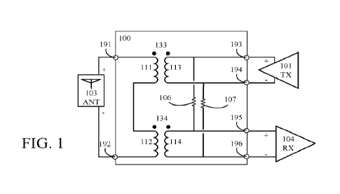
Figure 1 schematically illustrates an example arrangement according to some
embodiments.
Figure 1 shows an example antenna interface arrangement 100 for cancellation
of a transmit
signal at a receiver port of a transceiver. Example connection of the antenna
interface
arrangement to a transmitter (TX) 101, a receiver (RX) 104, and an antenna
(ANT) 103 of a
transceiver is also shown.
The antenna interface arrangement 100 comprises an impedance (illustrated in
Figure 1 as
two resistors 106, 107) and a distributed transformer. The distributed
transformer has a
primary side winding with a first part 111 and a second part 112, a first
secondary side winding
113, and a second secondary side winding 114. The first secondary side winding
113 has a first
inductive coupling 133 to the first part 111 of the primary side winding, and
the second
secondary side winding 114 has a second inductive coupling 134 to the second
part 112 of the
primary side winding.
In the transceiver exemplified in Figure 1, the transmitter port, the receiver
port, and the
antenna port are differential ports having a positive terminal and a negative
terminal.
A first end of the first part 111 of the primary side winding is connectable
to one of the
terminals 191 (terminal "+" in this example) of the antenna port of the
transceiver, a second
end of the first part 111 of the primary side winding is connected to a first
end of the second
part 112 of the primary side winding, and a second end of the second part 112
of the primary
side winding is connectable to the other one of the terminals 192 (terminal "-
" in this
example) of the antenna port of the transceiver.
A first end of the first secondary side winding 113 is connectable to one of
the terminals 193
(terminal "+" in this example) of the transmitter port of the transceiver, and
a second end of
the first secondary side winding 113 is connectable to the other one of the
terminals 194
(terminal "-" in this example) of the transmitter port of the transceiver.
CA 03172517 2022- 9- 20
WO 2021/185458
PCT/EP2020/057848
A first end of the second secondary side winding 114 is connectable to one of
the terminals
195 (terminal "+" in this example) of the receiver port of the transceiver,
and a second end of
the second secondary side winding 114 is connectable to the other one of the
terminals 196
(terminal "-" in this example) of the receiver port of the transceiver.
5 The impedance is connected between the first secondary side winding 113
and the second
secondary side winding 114. More specifically, in this implementation, the
resistor 106 is
connected between the first end of the first secondary side winding and the
first end of the
second secondary side winding, and the resistor 107 is connected between the
second end of
the first secondary side winding and the second end of the second secondary
side winding.
10 Generally, the first and second inductive couplings are adapted to
provide a first version of the
transmit signal at the receiver port, and the impedance is adapted to provide
a second version
of the transmit signal at the receiver port. Also generally, it is an aim that
the second version
of the transmit signal cancels the first version of the transmit signal. One
way to achieve this is
to provide the second version of the transmit signal as having the same
amplitude and
opposite phase as the first version of the transmit signal.
In the implementation shown in Figure 1, the first and second inductive
couplings 133, 134 are
non-inverting inductive couplings, and the resistors are coupled between
transmitter and
receiver ports with the same polarity (i.e., one resistor 106 is connected
between the positive
terminal "+"of the transmitter port and the positive terminal "+" of the
receiver port, and the
other resistor 107 is connected between the negative terminal "-" of the
transmitter port and
the negative terminal "-" of the receiver port). Thereby, a phase impact of
the first and second
inductive couplings 133, 134 on the transmit signal and a phase impact on the
transmit signal
of the impedance 106, 107 has a modulo 27r phase difference equal to it (i.e.,
opposite
phases) for a periodic transmit signal.
The impedance 106, 107 should preferably be selected such that cancellation of
transmit
signal leakage to the receiver port is achieved and/or such that cancellation
of received signal
leakage to the transmitter port is achieved. This may, for example, be
accomplished by
selecting the impedance 106, 107 such that an amplitude impact of the first
and second
inductive couplings 133, 134 on the transmit signal is equal to an amplitude
impact on the
transmit signal of the impedance 106, 107.
CA 03172517 2022- 9- 20
WO 2021/185458
PCT/EP2020/057848
11
Other example antenna interface arrangements for cancellation of a transmit
signal at a
receiver port of a transceiver may be achieved by letting both first and
second inductive
couplings 133,134 be inverting inductive couplings in Figure 1.
Generally, it should be noted that one or more of the antenna interface
arrangements
exemplified herein (e.g., the example antenna interface arrangement 100 of
Figure 1) may
also provide cancellation of a received signal at the transmitter port of the
transceiver.
Particularly, the first inductive coupling may be further adapted to provide a
first version of
the received signal at the transmitter port, and the second inductive coupling
and the
impedance may be further adapted to provide a second version of the received
signal at the
transmitter port. Also generally, it is an aim that the second version of the
received signal
cancels the first version of the received signal. One way to achieve this is
to provide the
second version of the received signal as having the same amplitude and
opposite phase as the
first version of the received signal, which one or more of the antenna
interface arrangements
exemplified herein achieve.
Also generally (assuming that the antenna port is port 1, the transmitter port
is port 2, and the
receiver port is port 3, and that S12 represents the coupling from transmitter
to antenna, S31
represents the coupling from antenna to receiver, S32 represents the coupling
from
transmitter to receiver, and S23 represents the coupling from receiver to
transmitter), it
should be noted that the stand-alone transformer used in some embodiments
herein allows
sharing an antenna between transmitter and receiver (e.g., resulting in a
coupling loss of
S12 = S31 = ¨3dB for a transformer with identical windings), wherein the
transmitter and
receiver are magnetically connected by the transformer (e.g., S32 = S23 = ¨6dB
for a
transformer with identical windings). Isolation between transmitter and
receiver is obtainable
by using adequately connected resistors (or general impedances). Since no
resonance is
introduced, the theoretical bandwidth is infinite when the inductors are
magnetically coupled.
The magnetic connection between transmitter and receiver introduces 180 phase
rotation if
the inductive couplings 133 and 134 are either both non-inverting or both
inverting, and
isolation between transmitter and receiver is obtainable by connecting
resistors between port
terminals of the same polarity.
CA 03172517 2022- 9- 20
WO 2021/185458
PCT/EP2020/057848
12
The magnetic connection between transmitter and receiver introduces no phase
rotation if
one of the inductive couplings is non-inverting and the other one of the
inductive couplings is
inverting, and isolation between transmitter and receiver is obtainable by
connecting resistors
between port terminals of different polarity.
Figure 2 schematically illustrates an example arrangement according to some
embodiments.
Figure 2 shows an example antenna interface arrangement for cancellation of a
transmit signal
at a receiver port of a transceiver when connected to a differential port
transmitter (TX) 101, a
differential port receiver (RX) 104, and a differential port antenna (ANT) 103
of a transceiver.
The boundary of the antenna interface arrangement (compare with 100 of Figure
1) and the
transceiver ports (compare with 191, 192, 193, 194, 195, 196 of Figure 1) are
omitted for
simplicity of representation.
The antenna interface arrangement comprises an impedance (illustrated in
Figure 2 as two
resistors 206, 207) and a distributed transformer. The distributed transformer
has a primary
side winding with a first part 211 and a second part 212, a first secondary
side winding 213,
and a second secondary side winding 214. The first secondary side winding 213
has a first
inductive coupling 233 to the first part 211 of the primary side winding, and
the second
secondary side winding 214 has a second inductive coupling 234 to the second
part 212 of the
primary side winding.
A first end of the first part 211 of the primary side winding is connectable
to one of the
terminals (terminal "+" in this example) of the antenna port of the
transceiver, a second end
of the first part 211 of the primary side winding is connected to a first end
of the second part
212 of the primary side winding, and a second end of the second part 212 of
the primary side
winding is connectable to the other one of the terminals (terminal "-" in this
example) of the
antenna port of the transceiver.
A first end of the first secondary side winding 213 is connectable to one of
the terminals
(terminal "+" in this example) of the transmitter port of the transceiver, and
a second end of
the first secondary side winding 213 is connectable to the other one of the
terminals (terminal
"-" in this example) of the transmitter port of the transceiver.
CA 03172517 2022- 9- 20
WO 2021/185458
PCT/EP2020/057848
13
A first end of the second secondary side winding 214 is connectable to one of
the terminals
(terminal "+" in this example) of the receiver port of the transceiver, and a
second end of the
second secondary side winding 214 is connectable to the other one of the
terminals (terminal
"-" in this example) of the receiver port of the transceiver.
The impedance is connected between the first secondary side winding 213 and
the second
secondary side winding 214. More specifically, in this implementation, the
resistor 206 is
connected between the first end of the first secondary side winding and the
second end of the
second secondary side winding, and the resistor 207 is connected between the
second end of
the first secondary side winding and the first end of the second secondary
side winding.
In the implementation shown in Figure 2, the first inductive coupling 233 is a
non-inverting
inductive coupling, the second inductive coupling 234 is an inverting
inductive coupling, and
the resistors are coupled between transmitter and receiver ports of different
polarity (i.e., one
resistor 206 is connected between the positive terminal "+"of the transmitter
port and the
negative terminal "-" of the receiver port, and the other resistor 207 is
connected between the
negative terminal "-" of the transmitter port and the positive terminal "+" of
the receiver
port). Thereby, a phase impact of the first and second inductive couplings
233, 234 on the
transmit signal and a phase impact on the transmit signal of the impedance
206, 207 has a
modulo 27 phase difference equal to TT (i.e., opposite phases) for a periodic
transmit signal.
The impedance 206, 207 should preferably be selected such that cancellation of
transmit
signal leakage to the receiver port is achieved and/or such that cancellation
of received signal
leakage to the transmitter port is achieved. This may, for example, be
accomplished by
selecting the impedance 106, 107 such that an amplitude impact of the first
and second
inductive couplings 233, 234 on the transmit signal is equal to an amplitude
impact on the
transmit signal of the impedance 206, 207.
Other example antenna interface arrangements for cancellation of a transmit
signal at a
receiver port of a transceiver may be achieved by letting the first inductive
coupling 233 be an
inverting inductive coupling and letting the second inductive coupling 234 be
a non-inverting
inductive coupling in Figure 1.
Figure 3 schematically illustrates an example arrangement according to some
embodiments.
CA 03172517 2022- 9- 20
WO 2021/185458
PCT/EP2020/057848
14
Figure 3 shows an example antenna interface arrangement 300 for cancellation
of a transmit
signal at a receiver port of a transceiver. Example connection of the antenna
interface
arrangement to a transmitter (TX) 301, a receiver (RX) 304, and an antenna
(ANT) 303 of a
transceiver is also shown.
The antenna interface arrangement 300 comprises an impedance (illustrated in
Figure 3 as
resistor 306) and a distributed transformer. The distributed transformer has a
primary side
winding with a first part 311 and a second part 312, a first secondary side
winding 313, and a
second secondary side winding 314. The first secondary side winding 313 has a
first inductive
coupling 333 to the first part 311 of the primary side winding, and the second
secondary side
winding 314 has a second inductive coupling 334 to the second part 312 of the
primary side
winding.
In the transceiver exemplified in Figure 3, the transmitter port, the receiver
port, and the
antenna port are single-ended ports.
A first end of the first part 311 of the primary side winding is connectable
to the antenna port
391 of the transceiver, a second end of the first part 311 of the primary side
winding is
connected to a first end of the second part 312 of the primary side winding,
and a second end
of the second part 312 of the primary side winding is connectable to a
reference potential
(e.g., a ground potential).
A first end of the first secondary side winding 313 is connectable to the
transmitter port 393 of
the transceiver, and a second end of the first secondary side winding 313 is
connectable to a
reference potential (e.g., a ground potential).
A first end of the second secondary side winding 314 is connectable to the
receiver port 395 of
the transceiver, and a second end of the second secondary side winding 314 is
connectable to
a reference potential (e.g., a ground potential).
The impedance 306 is connected between the first end of the first secondary
side winding 313
and the first end of the second secondary side winding 314.
In the implementation shown in Figure 3, the first and second inductive
couplings 333, 334 are
non-inverting inductive couplings. Thereby, a phase impact of the first and
second inductive
couplings 333, 334 on the transmit signal and a phase impact on the transmit
signal of the
CA 03172517 2022- 9- 20
WO 2021/185458
PCT/EP2020/057848
impedance 306 has a modulo 27( phase difference equal to m (i.e., opposite
phases) for a
periodic transmit signal.
The impedance 306 should preferably be selected such that cancellation of
transmit signal
leakage to the receiver port is achieved and/or such that cancellation of
received signal
5 leakage to the transmitter port is achieved. This may, for example, be
accomplished by
selecting the impedance 106, 107 such that an amplitude impact of the first
and second
inductive couplings 333, 334 on the transmit signal is equal to an amplitude
impact on the
transmit signal of the impedance 306.
Other example antenna interface arrangements for cancellation of a transmit
signal at a
10 receiver port of a transceiver may be achieved by letting both first and
second inductive
couplings 133, 134 be inverting inductive couplings in Figure 3.
Part (a) of Figure 4 schematically illustrates an adjusted example arrangement
according to
some embodiments. The adjusted example antenna interface arrangement of part
(a) in
Figure 4 is similar to the example antenna interface arrangement 100
illustrated in Figure 1,
15 with the addition of one or more circuit elements 421, 423, 424.
Corresponding adjustments ¨
i.e., addition of one or more circuit elements ¨ may be applied in relation to
any of the other
example antenna interface arrangements described herein (e.g., in Figure 2, or
in Figure 3).
The adjusted example antenna interface arrangement of part (a) in Figure 4 is
for cancellation
of a transmit signal at a receiver port of a transceiver. Example connection
of the antenna
interface arrangement to a transmitter (TX) 401, a receiver (RX) 404, and an
antenna (ANT)
403 of a transceiver is also shown.
In similarity with Figure 1, the antenna interface arrangement comprises an
impedance
(exemplified as two resistors 406, 407) and a distributed transformer. The
distributed
transformer has a primary side winding with a first part 411 and a second part
412, a first
secondary side winding 413, and a second secondary side winding 414. The first
secondary
side winding 413 has a first inductive coupling to the first part 411 of the
primary side winding,
and the second secondary side winding 414 has a second inductive coupling to
the second part
412 of the primary side winding. The impedance and the distributed transformer
are arranged
in a similar manner as those of Figure 1.
CA 03172517 2022- 9- 20
WO 2021/185458
PCT/EP2020/057848
16
The antenna interface arrangement of part (a) in Figure 4 further comprises
one or more of a
first circuit element (e.g., an antenna port impedance 423), a second circuit
element (e.g., a
transmitter port impedance 421), and a third circuit element (e.g., a receiver
port impedance
424).
The first circuit element 423 may be connected in parallel to the primary side
winding 411,
412, the second circuit element 421 may be connected in parallel to the first
secondary side
winding 413, and the third circuit element 424 may be connected in parallel to
the second
secondary side winding 414, as illustrated in part (a) in Figure 4.
Generally, when an impedance is referred to herein it is meant to encompass
one or more of a
purely real valued impedance (resistance), a purely imaginary valued impedance
(capacitance
or inductance), and any combination thereof in the form of a complex valued
impedance.
Thus, any of the first, second, and third circuit element may comprise a real
valued part
and/or an imaginary valued part.
Any of the first, second, and third circuit element may be adapted to
compensate
imperfections of the distributed transformer and/or impedance mismatches, in
accordance
with any suitable compensation approach.
Antenna interface arrangements with addition of one or more port impedances as
exemplified
in part (a) in Figure 4, may be particularly useful when one or more of the
transceiver ports are
non-ideal. One or more of the port impedances may be tunable to accommodate
impedance
variations of one or more of the transceiver ports.
Part (b) of Figure 4 schematically illustrates an example arrangement
according to some
embodiments. The adjusted example antenna interface arrangement of part (b) in
Figure 4 is
similar to the example antenna interface arrangement 100 illustrated in Figure
1, but shows
the impedance in a more general implementation. Corresponding generalization ¨
i.e.,
switching one or more resistor to a complex valued impedance ¨ may be applied
for any of the
other example antenna interface arrangements described herein (e.g., in Figure
2, in Figure 3,
or in part (a) of Figure 4).
The antenna interface arrangement of part (b) in Figure 4 is for cancellation
of a transmit
signal at a receiver port of a transceiver. Example connection of the antenna
interface
CA 03172517 2022- 9- 20
WO 2021/185458
PCT/EP2020/057848
17
arrangement to a transmitter (TX) 401, a receiver (RX) 404, and an antenna
(ANT) 403 of a
transceiver is also shown.
In similarity with Figure 1, the antenna interface arrangement comprises an
impedance
(exemplified as two impedances 408, 409; each comprising a real valued part
and/or an
imaginary valued part) and a distributed transformer. The distributed
transformer has a
primary side winding with a first part 411 and a second part 412, a first
secondary side winding
413, and a second secondary side winding 414. The first secondary side winding
413 has a first
inductive coupling to the first part 411 of the primary side winding, and the
second secondary
side winding 414 has a second inductive coupling to the second part 412 of the
primary side
winding. The impedance and the distributed transformer are arranged in a
similar manner as
those of Figure 1.
In addition to the conditions for selecting impedance values described in
connection with
Figure 1, the complex valued impedances in part (b) of Figure 4 may be adapted
to
compensate imperfections of the distributed transformer and/or impedance
mismatches, in
accordance with any suitable compensation approach.
Generally, one or more of a size of the first part of the primary side
winding, a size of the
second part of the primary side winding, a size of the first secondary side
winding, a size of the
second secondary side winding, the impedance value (compare with 408, 409),
and the circuit
element value(s) (compare with 421, 423, 424) may be selected for matching of
transmitter
port impedance and/or receiver port impedance and/or antenna port impedance.
A distributed transformer, as applied in various embodiments herein, may have
any suitable
ratio (e.g., ratio 1:1, 1:2, etc.).
Figure 5 schematically illustrates an example apparatus 510 according to some
embodiments.
The apparatus 510 may, for example, be a communication device. The apparatus
comprises a
transceiver (TX/RX) 530 and an antenna interface arrangement (Al) 500. The
transceiver may
be a full-duplex transceiver or a half-duplex transceiver. Alternatively or
additionally, the
transceiver may be a TDD transceiver. The antenna interface arrangement 500
may be any of
the antenna interface arrangements described in connection to Figures 1-4.
CA 03172517 2022- 9- 20
WO 2021/185458
PCT/EP2020/057848
18
Generally, the distributed transformers of the various embodiments presented
herein may be
implemented in any suitable manner. The distributed transformer may be an
ideal
transformer (coupling factor k = 1) or a non-ideal transformer (coupling
factor k < 1, e.g.,
k = 0.85). Some loss may result from using a non-ideal transformer and the
phase shift may
not be perfect (i.e., 0' or 1800). However, the isolation and noise figure of
the antenna
interface arrangement are mainly determined by the cancellation impedance, and
remain
relatively low even for non-ideal transformers.
Also generally, each of the impedances and/or circuit elements exemplified
herein may
comprise a real valued part and/or an imaginary valued part, as suitable (even
if exemplified
as purely resistive in any of the Figures). For example, an impedance and/or a
circuit element
may be purely resistive, purely capacitive, purely inductive, or any
combination thereof.
Furthermore, an impedance and/or a circuit element may be implemented using
any suitable
means (e.g., connecting resistor(s), capacitor(s), coil(s) in any parallel
and/or serial
arrangement).
Typically, the cancellation impedances (106, 107, 206, 207, 306, 406, 407,
408, 409) may be
selected based on (e.g., equal to, or with equal absolute value as,
corresponding) port
impedances.
To accommodate challenges caused by a non-ideal transformer (and/or non-ideal
impedances
of transmitter/receiver/antenna ports), one or more reactive elements may be
introduced in
the antenna interface arrangement (e.g., to obtain the desirable cancelling
phase difference).
Figure 4 represents examples of how this may be implemented.
One embodiment targeting a non-ideal transformer comprises the impedances 408,
409
illustrated in part (b) of Figure 4; each comprising a functionally serial
connection of a
resistance and an inductance.
One embodiment targeting non-ideal impedances of transmitter/receiver/antenna
ports uses
the arrangement illustrated in Figure 3 for impedance matching by sizing the
windings of the
transformer to achieve desirable matching for transmitter and receiver ports.
For example,
assuming that the antenna port experiences 500, the transmitter port
experiences 300 and
the receiver port experiences 700, the resistor 306 may be selected close to
the 300 of the
CA 03172517 2022- 9- 20
WO 2021/185458
PCT/EP2020/057848
19
transmitter port (e.g., 350), the first and second parts 311, 312 of the
primary side winding
may be equally sized, the first secondary side winding 313 may be sized to one
third of the
first part 311 of the primary side winding, and the second secondary side
winding 314 may be
sized to seven fifths of the second part 312 of the primary side winding.
Embodiments may appear within an electronic apparatus (such as a transceiver
or a
communication device) comprising arrangements, circuitry, and/or logic
according to any of
the embodiments described herein.
Generally, all terms used herein are to be interpreted according to their
ordinary meaning in
the relevant technical field, unless a different meaning is clearly given
and/or is implied from
the context in which it is used.
Reference has been made herein to various embodiments. However, a person
skilled in the art
would recognize numerous variations to the described embodiments that would
still fall
within the scope of the claims.
It should be noted that in the description of embodiments, the partition of
functional blocks
into particular units is by no means intended as limiting. Contrarily, these
partitions are merely
examples. Functional blocks described herein as one unit may be split into two
or more units.
Furthermore, functional blocks described herein as being implemented as two or
more units
may be merged into fewer (e.g. a single) unit.
Any feature of any of the embodiments disclosed herein may be applied to any
other
embodiment, wherever suitable. Likewise, any advantage of any of the
embodiments may
apply to any other embodiments, and vice versa.
Hence, it should be understood that the details of the described embodiments
are merely
examples brought forward for illustrative purposes, and that all variations
that fall within the
scope of the claims are intended to be embraced therein.
CA 03172517 2022- 9- 20