Note: Descriptions are shown in the official language in which they were submitted.
WO 2021/191307 1
PCT/EP2021/057628
ELECTRON MICROSCOPY SUPPORT
This application claims priority from GB2004272.7 filed 24 March 2020, the
contents and
elements of which are herein incorporated by reference for all purposes.
Field of the Disclosure
The present invention relates to an electron microscopy (EM) sample support; a
method of
manufacturing an electron microscopy sample support; a method of imaging using
an electron
microscopy sample support and an apparatus operable to perform a method of
imaging. The
support is particularly useful in cryoEM imaging.
Background
Electron microscopy techniques can be used to image a specimen. According to
such
techniques, a beam of electrons is used to 'illuminate' a specimen. The
presence of the
specimen in the electron beam results in changes to that beam. The changes to
the beam
induced by the sample can be examined to create a magnified image of the
specimen.
In order to be illuminated by an electron beam, a specimen must be adequately
supported in
that beam. Often the electrons forming the electron beam have a high energy
and it will be
appreciated that bombarding an object, for example, a specimen for
examination, together with
the support holding the specimen in position within the electron beam, may
result in physical,
chemical and/or electrical changes to the support and/or specimen. Such
changes may impact
results, including resolution of image, obtained through use of electron
microscopy techniques.
In this regard, at least two outstanding problems exist in the field. Firstly,
specimen movement
at the beginning of electron beam irradiation in particular degrades image
quality and removes
information about the undamaged molecules from the structure. Thus, all
current EM structural
determination models have varying degrees of radiation damage incorporated.
Secondly, the
throughput of modern synchrotron crystallography beam lines vastly exceeds
that of current
state-of the art electron microscopes, at least in part due to current
limitations in EM specimen
supports, meaning that although high resolution structure determination for
drug discovery and
CA 03172576 2022- 9- 21
WO 2021/191307 2
PCT/EP2021/057628
development is feasible by EM techniques, throughput is low so use of this
technique is limited
in practice.
Ermantraut 1998 describes a carbon support foil ("Quantifoil" 0) for cryoEM
and aims to
minimize the total specimen thickness to eliminate the object distortions
arising from interaction
with the support structure. The foil has square holes that support ice layers
having a thickness
down to 32 2.3 nm. One carbon foil is said to be 15 nm thick and it is
stated (but not shown)
that a hole diameter as small as 500 nm was formed. This corresponds to a hole
diameter to
thickness ratio of 33.3:1.
Janbroers 2009 describes carbon-free temperature-stable TEM grids. An 80%
Au/20% Pd metal
film is supported on standard mixed-mesh Au TEM grids. The grids are formed by
applying the
metal to a carbon-covered TEM grid followed by selective removal of the carbon
using plasma
cleaning. The circular holes shown in the figures therein are approximately
1.5 pm or more in
diameter. The 80% Au/20% Pd metal film thickness was set to 7, 10 or 15 nm.
This corresponds
to a smallest hole diameter to thickness ratio of 100:1. The average grain
size is 8.3 nm 2.0
nm and deposition occurs at room temperature.
Grant-Jacob 2016 describes three-dimensionally structured gold membrane films
with
nanopores of defined, periodic geometries that are intended to provide
spatially localised
enhancement of electric fields by manipulation of the plasmons inside the
nanopores. Because
these films are not flat they are unsuitable for suspending a sample for
analysis by electron
microscopy. The substrate contains an array of inverted pyramids etched into a
4 mm x 4 mm
square region on the surface with inverted pyramids of 1.5 pm x 1.5 pm square,
1 pm deep with
a pitch of 2 pm and a thickness of 100 nm. a nano-sized hole of 50 nm square
was milled
through the gold film at a specific location in the cavity to provide electric
field control which can
subsequently used for enhancement of fluorescence or Raman scattering of
molecules in the
nanopore. This corresponds to a hole diameter to thickness ratio at the tip of
the pyramidal
structure of 2:1. However, the walls of the hole are not thick enough to
support a sample film.
The average grain size is -40 nm and deposition occurs at room temperature.
CA 03172576 2022- 9- 21
3
WO 2021/191307
PCT/EP2021/057628
Jia 2019 describes large-area freestanding gold nanomembranes that are 50 nm
or more in
thickness with nanoholes through the membrane having a diameter of 250 nm.
This
corresponds to a hole diameter to thickness ratio of 5:1. However, the gold
nanomembranes are
formed by room temperature deposition and as a result they do not provide an
improvement in
image quality as significant as the present invention.
Previous work by the present inventors includes Russo 2014 where a gold
specimen support
that nearly eliminates substrate motion during irradiation is shown. The
support therein is a gold
foil having a -500 A thickness and 1.2 pm diameter holes in a square pattern.
This corresponds
to a hole diameter to thickness ratio of 24:1.
Also, in Russo 2016, an all-gold support is described that has a gold foil
having a -400 to 500 A
thickness and micrometer diameter holes. This corresponds to a hole diameter
to thickness
ratio of at least 20:1.
All of the known gold support foils mentioned above are at least 500 A thick.
This is because
foils of below about 500 A thick are not currently stable due to their
polycrystalline grain
structures which typically have mean grain sizes of about 200 nm or more. When
foils below
about 500 A thick are formed they suffer from structural deficiencies such as
gaps and cracks in
the structure of the foil which can contribute to a lack of structural
rigidity and therefore sample
movement, for example during any thermal expansion caused by electron-beam
heating.
Furthermore, holes through such films have significantly rough edges caused by
the individual
grains, which is particularly noticeable at the edges of very small holes.
This roughness
negatively impacts the ease of imaging and stabilisation. Moreover, thin gold
foils with hole
sizes of less than 0.5 pm, optimised for single particle cryoEM, cannot be
produced by standard
diffraction-limited photolithography.
It is desired to provide a support, for use in electron microscopy,
particularly cryoEM, which may
address some of the problems of known specimen supports, such as unwanted
movement
during imaging. The present disclosure has been devised in the light of the
above
considerations.
CA 03172576 2022- 9- 21
4
WO 2021/191307
PCT/EP2021/057628
Summary of the Disclosure
The present inventors have found that unwanted movement during transmission
electron
microscopy imaging using current supports for electron microscopy is caused at
least in part by
build-up of tensions in the specimen film which can lead to buckling of the
film when forces
exceed a certain threshold. For example, tensions build-up in vitreous ice
films used to
immobilise samples for cryoEM, with a buckling threshold that depends directly
on the shape of
the specimen film. Taking cryoEM as an example, during cryoplunging to freeze
the aqueous
sample, freezing occurs over a time interval of 10-4 seconds. Within this
time, the water
density change is most rapid near the homogeneous nucleation temperature 235K.
As the water
solidifies, the rapid cooling does not allow sufficient time for structural
rearrangements of the
water molecules resulting in the accumulation of compressive strain within the
thin ice film. If
compression exceeds a critical value, the ice film buckles, thus momentarily
relieving the radial
stress in the layer.
Buckling only occurs if the stress exceeds a critical point, which is
determined by the
dimensions of the ice film, its elastic moduli, specific volume change
relative to the support, and
the constraints at the edge of the hole. As the vitreous ice film continues to
cool to the
temperature of the surrounding cryogen, typically liquid ethane at 90 to 93K,
more stress may
build up due to further relative density changes. This stress is stored in the
film indefinitely once
it fully cools down to and rests at 77K (liquid nitrogen temperature).
Even in situations where stress build-up in the ice layer does not exceed the
threshold to result
in buckling of that layer, when the sample is exposed to the electron beam in
a transmission
electron microscope (TEM), the localised heating can allow retained stresses
to be at least
partially relieved resulting in sample movement.
Put simply, the inventors found that buckling threshold of the film depends on
the shape and
dimensions of the film which is in turn determined by the shape of the hole it
is suspended in.
The present invention is devised to minimise or avoid the unnecessary build-up
of stress in films
to reduce, or completely eliminate, sample movement, caused, for example by
buckling or relief
of stresses on examination. This greatly improves image quality.
CA 03172576 2022- 9- 21
5
WO 2021/191307
PCT/EP2021/057628
In a first aspect there is provided a support for an electron microscopy
sample, the support
comprising a metallic foil having one or more holes therethrough wherein
thickness of the
metallic foil is less than 50 nm and/or the mean linear intercept grain size
is 50 nm or less,
wherein the ratio of the diameter of each hole to the thickness of the
metallic foil is 15:1 or less,
and wherein the metallic foil consists of either (a) one or more metals
selected from transition
metals, aluminium and beryllium, or an alloy thereof; or (b) degenerately
doped silicon wherein
the dopant element is selected from boron, aluminium, boron and arsenic at a
concentration of
1020 atoms/cm3 or higher.
Notably, any alternatives within the first aspect are corresponding technical
features of these
proposals because they achieve the same technical effect of reducing sample
movement to
solve the same technical problem of improving imaging.
Transition metals are elements in groups 3 to 11 of the periodic table of
elements.
In some cases, some or all of the one or more transition metals are selected
from one or more
of noble metals (ruthenium, rhodium, palladium, silver, osmium, iridium,
platinum, gold), copper,
molybdenum, titanium, nickel, chromium, tungsten, hafnium, and tantalum or an
alloy thereof.
Preferably the one or more transition metals are selected from the noble
metals ruthenium,
rhodium, palladium, silver, osmium, iridium, platinum, gold or an alloy
thereof. Preferably the
one or more transition metals are selected from gold, palladium and platinum
or an alloy
thereof. Preferably the metallic foil comprises or consists of gold or an
alloy thereof. Preferably
the alloy is a binary alloy. Particularly preferred alloys include gold-silver
alloy, gold-copper
alloy, nickel-titanium alloy, gold-platinum alloy and platinum-iridium alloy.
It may be that the foil
does not comprise aluminium. It may be that the foil does not comprise
beryllium. It may be that
the foil does not comprise an alloy.
For the avoidance of doubt, the metallic foil is not formed from an electrical
insulator, a semi-
conductor material or a carbon material such as amorphous or graphitic carbon,
although these
may be present in a metallic alloy as described herein. Semi-conductor
materials include
materials whose conductivity drops with decreasing temperature in the 300 to
80K range. This
includes carbon (amorphous or graphitic but not diamond), silicon (below
1020/cm3 doping with a
CA 03172576 2022- 9- 21
WO 2021/191307 6
PCT/EP2021/057628
dopant element such as boron, aluminium, phosphorus and arsenic), gallium
arsenide and other
III-V or II-VI binary semiconductors.
In some cases, the ratio of the diameter of each hole to the thickness of the
metallic foil is 11:1
or less, 10:1 or less, 8:1 or less, 7:1 or less, or 5:1 or less. The ratio of
each hole diameter to
the foil thickness may be between 11:1 and 1:1, 10:1 and 2:1, 9:1 and 3:1 or
8:1 and 4:1.
An advantage of using the specified ratios is that it eliminates buckling of
specimen films when
such films are formed in the holes, such as a suspended amorphous ice film
that are used in
cryoEM. This allows precise foil tracking during imaging with high-speed
detectors, lessening
demands on cryostage precision and stability. The present support therefore
reduces particle
movement to the limit set by pseudo-diffusion, which is less than the
resolution of the electron
cryomicroscope. This allows reconstruction of a complete map at 1.9 A
resolution with a fluence
of < 1 e-/A2 at 300 keV. The specimen films remain stable and under radial
compression
throughout irradiation, and only diffusive movement occurs which is limited to
< 1 A RMS in 30
e-/A2. The present movement-suppressing microscopy specimen support allows
atomic
structure determination at only 1 e-/A2, and extrapolation back to the point
before destructive
effects of electron radiation affect the reconstruction.
In some cases the metallic foil is substantially free of structural defects. A
lack of structural
defects means that the foil material is substantially uniform and continuous.
That is to say, there
are no gaps or cracks visible in the foil and the surface roughness is
reduced. For example, the
edge roughness of each hole may be 20 nm or less, 15 nm or less, 10 nm or less
or 5 nm or
less as measured by the root mean square deviation from the expected
theoretical hole edge
profile. The foil may have only one structural defect that is up to 1 nm in
diameter per 100 nm2
area.
An advantage when the thickness of the metallic foil is less than 50 nm and is
free from
structural defects is that the foil is structurally stable and may be used to
generate much higher
resolution images by electron microscopy than were previously possible.
Moreover, the
decreased foil thickness provides thinner specimen films in the holes which
have an improved
transmission. Known metallic foils having a thickness of less than 50 nm are
not suitable for
CA 03172576 2022- 9- 21
7
WO 2021/191307
PCT/EP2021/057628
electron microscopy because they provide poor images, often fall apart (i.e.
they are not free
standing or cannot be suspended across an EM grid square such as a 50 pm grid
square,
without damage) and cannot adequately suspend sample films.
An advantage when the mean linear intercept grain size being 50 nm or less is
a lack of
structural defects in combination with a decrease in the roughness of the
surface, particular in
the edges of the holes, such that the metallic foil may be successfully
employed in very high
resolution electron microscopy. Foils of these grain sizes are known, but all
suffer from
structural defects and non-uniformity which makes them unsuitable for electron
microscopy,
especially at high resolutions. Such known foils are typically formed as a
deposit on a
supporting surface. By contrast, the present metallic foils are robust enough
to be self-
supporting when suspended across an opening, for example a 50 pm grid square
in a TEM grid.
Therefore the foils of the present disclosure are preferably unsupported, i.e.
they are not
provided on a supporting layer. The specific grain sizes and lack of
structural defects of the
present metallic foil allow for the formation of rounder and smoother
nanoscale holes that
provide stable support for suspending a sample.
In some cases, the metallic foil thickness is 49 nm or less, such as 45 nm or
less, 40 nm or less,
30nm or less, 20 nm or less, 10 nm or less or 5 nm or less. The metallic foil
thickness is
preferably substantially constant throughout. Preferably, the foil thickness
may fluctuate by up to
only 25 A, 10 A or 5 A throughout.
In some cases, the mean linear intercept grain size of the metallic foil
material may be 40 nm or
less, such as 30 nm or less, 20 nm or less, 10 nm or less or 5 nm or less.
Lower grain sizes
provides increasing stability to the foil at lower thicknesses. A mean linear
intercept grain size of
10 nm or less is particularly preferred for an optimum balance of the
advantages.
In some cases, the diameter of each hole is 750 nm or less, 700 nm or less,
such as 600 nm or
less, 500 nm or less, 400 nm or less, 350 nm or less, 330 nm or less, 300 nm
or less, 250 nm or
less, 200 nm or less, 180 nm or less, 150 nm or less, 100 nm or less, or 75 nm
or less. In some
cases the diameter of each hole is in a range selected from 750 nm to 75 nm,
500 nm to 100
nm, 400 nm to 150 nm, 300 nm to 150 nm, or 250 nm to 150 nm. The holes are
preferably
CA 03172576 2022- 9- 21
WO 2021/191307 8
PCT/EP2021/057628
substantially circular. The holes may all be substantially the same diameter
or different
diameters. The diameter of each hole is preferably substantially the same
throughout the depth
of each hole. Each hole passes completely through the metallic foil. The
spacing between the
holes is preferably equal. The spacing between the holes is preferably equal
to at least one hole
diameter. The hole walls are preferably at a 90 degree angle to the surface of
the foil, optionally
with a precision of 2 degrees or better. For any hole diameter, the depth of
the holes is
preferably 500 nm or more. The side walls of the holes are preferably vertical
or retrograde
(tapered). These two preferences ensure the holes formed in the foil are not
likely to be
obstructed by material deposited at the bottom/sidewalls of the wells later in
the process. The
metallic foil may comprise other secondary holes that are greater than the
above specified
diameter requirement and/or do not meet the above diameter to foil thickness
requirement.
Because secondary holes do not meet the specified requirements they are
superfluous.
Alternatively, in some cases, the foil only comprises holes that meet the
specified requirements.
In some cases, the metallic foil does not comprise any holes that do not meet
the specified
nanoscale diameter and/or diameter to thickness ratio requirements.
An advantage of the nanoscale dimensions is that the movement of the particles
in the holes is
isotropic (the same in the plane of the support and perpendicular to it),
spatially uncorrelated,
and scales with the root of the incident electron fluence, as would be the
case for purely random
motion. By comparison, in the larger hole diameters of known supports there is
an abrupt,
spatially correlated unwanted displacement of the particles at the onset of
irradiation (e.g. in the
first 4 e-/A2). This is followed by a decreasingly correlated movement that
continues with
reduced speed to the end of the exposure.
Another advantage is that nanoscale dimensioned holes provide plasmon
resonances in the
visible range, which causes the support to appear yellow on reflection with
white light but blue
on transmission, a property which may be useful for characterising a specimen
before imaging
with electrons.
CA 03172576 2022- 9- 21
9
WO 2021/191307
PCT/EP2021/057628
In some cases, the support has a light wavelength transmittance maximum of
from 650 to 800
nm, such as from 700 to 750 nm or 714 nm. The foil support may have a
transmittance
minimum of from 500 to 600, such as from 625 to 675 or 645 nm.
In some cases, the purity of the metallic foil material is 90% or more,
preferably 99% or more;
even more preferably 99.999% or more (i.e. contains the stated % of the
relevant metallic
material).
In some cases, the holes are arranged in a regular pattern on the metallic
foil, such as a
hexagonal pattern or a square pattern. Preferably, the holes are arranges in a
hexagonal
pattern. The pattern is preferably regular. The hexagonal pattern provides
closer packing and
improves structural rigidity. The hexagonal pattern also allows faster
examination of multiple
holes by automated systems because the closer packing of the holes in the film
results in a
shorter distance between one hole and the next which speeds up the time for
examination of
multiple holes.
In some cases, the metallic foil is provided on an EM support grid. The grid
provides additional
structural support to the foil. In some cases the foil and the grid are of
unitary construction. The
foil and the grid may be integrally formed. The foil and the grid may have the
same elemental
composition throughout. The foil and the grid may have different grain
structures. The
advantages provided by the grid and foil having the same elemental composition
include
increased stability during imaging because the two structures have the same
thermal expansion
coefficients, there is minimal, or no, difference in their mechanical
behaviour on thermal change
(heating or cooling) so little, or no, relative movement between the two
structures. Despite
having the same elemental composition, the crystal grain structure
requirements for the grid
material are not as rigorous as for the metallic foil so the foil and grid may
have different crystal
grain structures, e.g. grain sizes. The grid may be millimetre sized, such
circular grids having
diameter of 5 mm, 4 mm or, most preferably 3 mm. The grid may comprise one or
more support
bars arranged to form a mesh across which the foil can be suspended. In some
cases, the
mesh has a mean hole size that is on a micrometre scale, such as about 300 pm,
about 200 pm
about 100 pm, or about 50 pm. The mesh holes may be hexagonal or square.
Preferably, the
CA 03172576 2022- 9- 21
WO 2021/191307 10
PCT/EP2021/057628
mesh holes have a hexagonal shape. Preferably the mesh holes tessellate, i.e.
if then holes are
square they are arranged in a square array and if they are hexagonal they are
arranged in a
hexagonal array. The hexagonal holes and array provides closer packing and
improves
structural rigidity. The mesh hole pattern may correspond to the foil hole
pattern.
In some cases, the grid is formed from a material that is selected from the
same options listed
herein for the metallic foil. In some cases the grid comprises one or more
metals selected from
transition metals, aluminium and beryllium, or an alloy thereof. It may be
that the one or more
transition metals are selected from one or more of noble metals (ruthenium,
rhodium, palladium,
silver, osmium, iridium, platinum, gold), copper, molybdenum, titanium,
nickel, chromium,
tungsten, hafnium, and tantalum or an alloy thereof. Preferably the one or
more transition
metals are selected from the noble metals ruthenium, rhodium, palladium,
silver, osmium,
iridium, platinum, gold or an alloy thereof. Preferably the one or more
transition metals are
selected from gold, palladium and platinum or an alloy thereof. Preferably the
grid comprises or
consists of gold or an alloy thereof. Preferably the alloy is a binary alloy.
Particularly preferred
alloys include gold-silver alloy, gold-copper alloy, nickel-titanium alloy,
gold-platinum alloy and
platinum-iridium alloy. It may be that the grid does not comprise aluminium.
It may be that the
grid does not comprise beryllium. It may be that the grid does not comprise an
alloy.
In some cases, the grid comprises degenerately doped silicon having a dopant
element
selected from boron, aluminium, boron and arsenic at a concentration of 1020
atoms/cm3 or
higher.
Hexagonal arrangement of the holes in both the metallic foil and the mesh
increases the usable
area tenfold over a standard cryoEM grid, allows more than 800 images to be
acquired from a
single stage position and provides more than 5000 individual holes in a single
25 pm wide
hexagonal mesh hole, for example.
In some cases, the electron microscopy is transmission electron microscopy,
preferably
transmission electron cryo-microscopy.
The grid or mesh that may be present as a support for the metallic film may,
in some cases be
arranged within a support rim. The options for the material used for the
support rim are the
CA 03172576 2022- 9- 21
WO 2021/191307 11
PCT/EP2021/057628
same as those for the grid described above. Preferably the support rim is
integral with the grid
structure.
In a second aspect there is provided the use of the support of the first
aspect in electron
microscopy, optionally in transmission electron microscopy, preferably in
transmission electron
cryo-microscopy.
In a third aspect there is provided a method of manufacturing a metallic foil
for a support
according to the first aspect comprising the steps of depositing a metallic
layer onto a patterned
substrate that is cooled to 200K or less to form a layer having a thickness of
50 nm or less and
having one or more holes therethrough; removing the deposited metallic layer;
and forming the
metallic layer into a support for an electron microscopy sample, wherein the
metallic foil consists
of either (a) one or more metals selected from transition metals, aluminium
and beryllium, or an
alloy thereof; or (b) degenerately doped silicon wherein the dopant element is
selected from
boron, aluminium, boron and arsenic at a concentration of 1020 atoms/cm3 or
higher.
By cooling the substrate in the deposition step it is possible to generate a
metallic layer thereon
that not only has a reduced grain size compared to deposition at room
temperature but also
have an excellent uniformity and continuity that is previously unknown at such
grain sizes,
particularly for gold and other suitably described metals and materials. This
is achieved
because the lower temperatures reduce the thermal energy of the atoms faster
than if the
surface was uncooled so reducing motion of the metal atoms on the deposition
surface once
they are deposited on the substrate. The atoms are rapidly immobilised upon
depositing upon
the substrate so the atoms move less and agglomerate into smaller grains than
if the surface
was uncooled.
In some cases the deposited foil is a metallic foil as described herein.
Furthermore, for many small EM samples, the desired foil hole size is a lower
diameter than the
diffraction limit of known photolithography techniques currently used to make
specimen
supports, and evaporated metal, in particular gold, foils below about 400 A
thick are not stable
(e.g. cannot be lifted from a deposition substrate without significant damage)
due to their
CA 03172576 2022- 9- 21
WO 2021/191307 12
PCT/EP2021/057628
polycrystalline grain structure. The present method affords metallic foils
that do not suffer from
these deficiencies.
In some cases, the patterned substrate is a silicon wafer, optionally between
3 mm and 300 mm
in diameter, such as 100 mm. The silicon wafer may be a degenerately doped
silicon wafer with
a resistivity <0.02 Ohm-cm. Alternatively, a silicon wafer with higher
resistivity of 1 to 30
Ohm-cm can be used. The silicon wafer may be formed by Talbot displacement
(phase
interference) lithography as described in Jefimovs 2017. The template-
substrate distance during
the phase interference lithography may be used to control the diameter of the
holes in the
silicon surface. A regular templating array can set the spacing between the
holes to be
patterned in the substrate. The silicon substrate is patterned so as to form
recesses therein to
correspond to the holes in the desired metallic foil.
In some cases the metallic foil may be formed integrally with a supporting
arrangement, e.g. a
mesh, of grid bars. In such a case, if it is desired to set the foil a certain
distance below the level
of the top surface of the grid bars, a mask with the grid bar pattern is
applied to the photoresist
coated silicon template to only expose the grid bar regions after developing.
These are then
etched, for example by reactive-ion etching (RI E), to make trenches at the
desired depth. This
step may be necessary to make the grids compatible with current specimen
plunging and
blotting apparatuses. If it is desired for the surface of the foil to be level
with the top surface of
the grid bars, this step is not required.
In some cases, there is a step of Bosch etching of the holes in the substrate.
This controls their
final depth and ensures the hole walls are at a 90 degree angle compared to
the surface of the
substrate with a precision of 2 degrees or better.
In some cases, there is a step of cleaning the patterned substrate before
deposition of the
metallic layer. The cleaning may be by immersion, for example in Piranha
solution (3H2SO4 :
1H202, freshly mixed), oxygen plasma or UV-Ozone plasma. Cleaning is
advantageous to
remove contaminants that can lead to poor hole formation.
In some cases, the metallic layer is deposited onto the patterned substrate
wherein the
substrate is at a temperature of 150K or less, 125K or less, 100K or less or
90K or less. The
CA 03172576 2022- 9- 21
WO 2021/191307 13
PCT/EP2021/057628
temperature of the substrate may be set from 84K to 92K. Preferably, to reduce
the grain size of
the metallic foil and allow for the formation of rounder, smoother holes
therethrough, the
substrate stage is kept at 77K (liquid nitrogen temperature) during the
evaporation. Higher
deposition rates require cooling to lower temperatures. The deposition may be
by electron beam
or thermal evaporation. For instance, the temperature range for nucleating 10
nm or smaller
crystals at 1 A/s deposition rates is 200K or less, assuming surface adatom
diffusion with
activation energy of 0.5 eV. The substrate having the deposited metallic layer
may be slowly
(about 50K/hour or slower) warmed up to room temperature in vacuum to prevent
the foil from
delaminating.
Preferably, for the best growth of the metallic crystals, the optimal
deposition temperature is
lower, due to the high-self diffusion coefficient of metallic materials, such
as gold. The purity of
material to be deposited is preferably 90% or more in order to form a stable
continuous layer,
more preferably 99% or more; even more preferably 99.999% or more.
In some cases, the patterned substrate is provided with a first sacrificial
layer applied to the
patterned substrate onto which the metallic layer is deposited. Any layer
which is selectively
etchable with respect to the relevant metallic foil layer can be used for this
layer. The sacrificial
layer may be a metal, such as copper (which is particularly preferred for gold
foils). It is
preferred that the sacrificial layer is copper. The sacrificial layer may also
be deposited on the
substrate under the cooling conditions described above. The deposition
conditions are
preferably the same for the sacrificial layer as the metallic foil layer. This
is preferred because
unwanted imperfections and roughness of the deposited sacrificial layer may
otherwise be
imparted to the side of the metallic foil layer formed thereon. The thickness
of the sacrificial
layer is preferably at least the same as the specified grain size. For example
a sacrificial layer
having a thickness of at least 10 nm, or at least 25 nm, or at least 50 nm may
be used. The
maximal thickness of the sacrificial layer is preferably less than the radius
of the holes in the foil.
In some cases there are one or more steps to transfer the metallic foil onto
an EM grid. The foil
may be transferred onto commercial EM grids using a float process.
Alternatively, the grids may
be directly fabricated on the substrate carrying the foil to afford an
integrated foil and grid. The
CA 03172576 2022- 9- 21
WO 2021/191307 14
PCT/EP2021/057628
latter is option is preferable for production on a large scale. The formation
of the foil integrally
with at least a mesh of grid bars and preferably the entire grid (mesh of grid
bars and thicker
grid circumference rim) is preferable because the use of the same metal for
both foil and grid
bars eliminates differences in thermal expansion coefficients and therefore
substrate movement
on heating (e.g. beam heating on exposure to an electron beam).
In some cases, the support is according to the first aspect.
Support production by transfer of the metallic foil to a commercial grid
To transfer the metallic foil to a commercial grid there may be steps of
lifting off, cleaning and
lowering the foil onto the grid. The foil may be coated with a 1 to 10 pm
layer of negative
photoresist before being lifted. The lifting step may include etching of a
sacrificial layer, such as
copper, to release the foil from the substrate. The cleaning step may be
performed by one or
more HCI washes (e.g. of 20%, 2%, 0.2% HCI, followed by at least three water
rinses). The
lowering step may include lowering a foil onto a clean grid by arranging the
grid on the bottom
of a dish filled with water in which the foil is floating and slowly syphoning
the water out. If a
supporting resist layer was used, it can then be removed by washing each
individual grid in the
appropriate solvents, and treating with low-energy plasma
Optionally, polymer-assisted graphene transfer, as described in Naydenova
2019, can be
carried out after the foil is lowered onto the girds.
Support production by integral formation of the grid on the metallic foil
To produce a support having an integrated metallic foil and grid, a
photoresist is temporarily
applied and the excess foil between adjacent prospective individual foils is
etched away. A
second temporary photoresist is applied so that grid bars, along with any
optional additional
features such as alignment marks, fiducials, labels, unique identifiers, can
be deposited by
electroplating. The photoresists are applied, exposed under a mask, developed
and removed
using standard techniques. After removing the second photoresist the surface
is cleaned with
an oxidative plasma or UV-Ozone. A supporting plastic layer is spun across the
grids. The
supports, now each comprising an integrated foil and a grid and supported
together on the
CA 03172576 2022- 9- 21
WO 2021/191307 15
PCT/EP2021/057628
same plastic layer, are then lifted off the substrate and cleaned, e.g. by a
series of 20 to 0.2%
aqueous hydrochloric acid and water washes.
The step of electrodeposition may form a deposited metallic layer totalling 10
to 15 pm in
thickness for the grid bars and rims. The metallic layer may be deposited from
an electrolyte
solution, preferably a non-cyanide bath, for example sulfite/thiosulfite. Such
a solution typically
has 10 to 15 g/L concentration of a metallic material to be deposited and is
used at 50 to 60 C
with an applied current density of 2 to 10 mA/cm2. Both of these parameters
are varied to
control the residual stress in the electroplated metallic layer. Under these
conditions, for
example, electroplated gold has Young's modulus of at least 35 GPa and
hardness of at least
40 Vickers.
The step of lifting off may include etching a sacrificial layer, such as
copper by chemical wet
etching, typically in ferric chloride or ammonium persulfate-based etchants.
The lifting off
preferably occurs in 20 minutes or less at room temperature, so as to prevent
the non-selective
etching of the metallic foil layer by the copper etchant. If the etching is
carried out at higher
temperature, the time is approximately halved for every 10 degrees of heating.
The grids may
be released from a silicon template by etching the silicon, preferably in a
hot (8000), agitated
solution of KOH (30%). The lift off occurs almost instantly on immersion into
the solution and is
accompanied by removal of the photoresist by the same solution. The individual
grids released
by this process may then be transferred in a clean bath of KOH, followed by
two deionized
water baths, a clean bath of piranha solution at room temperature (to remove
any copper), and
two more deionized water baths.
After the washing step, the integral supports are sufficiently stable on the
plastic layer for
packaging and shipping. The plastic layer can be removed by dissolving in an
appropriate
solvent immediately prior to use of each integral support. Any remaining small
traces of the
plastic can be removed by subsequent low-energy plasma treatment of the
cleaned grids. The
grids may be lowered onto a suitable support, e.g. filter paper, and dried
ready for use.
The requirements for a suitable plastic layer are therefore (i) to be easily
removable with
solvents, (ii) to be insoluble in water, HCI, copper etchant (either ammonium
persulfate or ferric
CA 03172576 2022- 9- 21
WO 2021/191307 16
PCT/EP2021/057628
chloride) and (iii) to have sufficient flexibility and structural rigidity for
the lifting off the substrate
and transferring to wash baths. Examples of suitable plastics include positive
or negative
photoresists, polystyrene and collodion.
Optionally, polymer-assisted graphene transfer, as described in Naydenova
2019, can be
carried out immediately after the deposition of the metallic foils to yield a
graphene layer
positioned between the foil and the grid bars. This is preferable in small
scale procedures.
Alternatively, it can be carried out after the grids are fully formed but
still attached to the wafer.
In this latter case, the plastic layer assisting the graphene transfer might
also be used as the
plastic layer, or an extra plastic layer may be added as described above. If a
large scale
procedure is used (e.g. wafer scale), the graphene can preferably be
transferred onto the grids
after their release from the wafer. This can be achieved, for example, by
transferring the grids
from the wafer onto another temporary supporting structure, for example a
suitable polymer that
can later be dissolved in organic solvents.
It has been determined that excellent support quality can be assured if one or
more of the
following parameters are met; (a) the fraction of clogged/malformed holes is <
1% (caused by
suboptimal cleanliness of the substrate prior to evaporation); (b) the
deviation from roundness
of the holes is < 10 nm (caused by insufficiently small grain size due to
elevated temperature
and/or deposition rate during evaporation, or by partial etching of the foil
during the lift off); (c)
the hole edge flatness is < 10 nm (as above, also caused by wear of the
template); (d) the grid
bar defect areas is < 1% (caused by defects in the masks); (e) the adhesion of
the foil to the
grid bars is sufficient to withstand stresses due to rapid cooling to from
277K to 80K (106 K/s or
faster) and (f) the foil coverage is > 99%.
These proposals also include an EM support as formed by a method described
herein.
In a fourth aspect there is provided a method of electron microscopy imaging
comprising a
step of sequentially imaging a sample suspended in a hole of a support
according to the first
aspect, wherein each image encompass at least a part of the edge of the hole
and the electron
beam encompasses the hole and the complete edge of the hole.
CA 03172576 2022- 9- 21
WO 2021/191307 17
PCT/EP2021/057628
In some cases, at least a part of the edge of the hole in each image is
compared to the other
images to remove any relative shift between sequential images and/or wherein
the sequential
images of the specimen in the hole are weighted to account for damage to the
specimen.
Summary of the Figures
So that the invention may be understood, and so that further aspects and
features thereof may
be appreciated, embodiments illustrating the principles of the invention will
now be discussed in
further detail with reference to the accompanying figures, in which:
Figure 1 shows movement of gold nanoparticles in vitreous ice in a range of
foil hole sizes.
Figure 1A shows typical drift-corrected electron micrograph used for tracking
gold particles in
vitreous water on all-gold supports; scale bar is 0.5 pm. The inset (20 nm x
20 nm) shows an
overlay of the initial and final positions of a gold nanoparticle at the
beginning of irradiation and
after a fluence of 60e-/A2.
Figures 1B and 1C show the root mean of the squared displacements of 200 to
2000 particles
from 10 to 50 movies of different diameter holes (UltrAuFoil R212- 1.9 pm,
UltrAuFoil R1.2/1.3 -
1.2 pm, UltrAuFoil R 0.6/1 - 0.8 pm, and custom made grids with 0.3 pm, and
0.2 pm holes) are
plotted as a function of cumulative electron fluence for 00 (B) and 300 tilt
(C). Error bars show
standard error in the mean. All exposures were under the same illumination
condition (300 kV,
2.4 pm beam diameter, 8 e-/A2/s). The ice thickness in all imaged holes was
300 50 A.
Figure 1D shows that thin films of ice used in cryoEM buckle during
vitrification if the
compressive stress (N) exceeds a critical value (No) determined by the aspect
ratio (2a/h) of the
film. Electron irradiation causes the film to move in response to additional
stresses in it, as
evident from the correlated particle movement at the beginning of irradiation.
Figure 2A shows a model of the stress accumulation in thin films of amorphous
ice during
cryoplunging and their response to electron irradiation. The density of liquid
and amorphous
water is plotted (stars) as a function of temperature, with a solid line to
guide the eye. During
cryoplunging into liquid ethane, water is rapidly cooled from, typically from
277K to 91K (arrow
at bottom). The largest specific volume change experienced by water below its
homogeneous
CA 03172576 2022- 9- 21
WO 2021/191307 18
PCT/EP2021/057628
nucleation point is (L,VN)mõ 5.5%. The thin film can only withstand
compression of up to
(AV/V)crit before it buckles (critical stress buildup range corresponds to a
300 A thick layer in a
1 pm hole).
Figure 2B shows the diffusivity of water molecules in liquid and amorphous ice
is plotted
(crosses) as a function of temperature. The solid line is a fit to these
values. The extrapolated
diffusivity in amorphous ice at 84K is vanishingly low, ¨10-46 A2/s. The
shaded region in the
bottom left indicates the range of diffusivity in amorphous ice at
temperatures in the 0 -100K
range, where it is stable indefinitely. During imaging with 300 keV electrons,
water molecules
move pseudo-diffusively by 1 A 2/(e-/A2). At typical imaging fluxes of 0.1 -10
e-/A2/s, this is
equivalent to 0.1 to 10 A2/s (shaded band between the top and middle) and
corresponds to an
instantaneous local temperature of 147K.
Figure 3 shows a foil that is an all-gold specimen support designed for
movement-free cryoEM
imaging. Figures 3A and 3B show optical micrographs, in (A) reflected and (B)
transmitted
unpolarized white illumination of the patterned gold foil (hexagonal array of
200 nm diameter
holes with 600 nm pitch) on a 600-mesh thin-bar gold grid. The scale and the
corresponding
area is the same for (A) and (B). The foil is blue in colour in transmitted
light is due to a strong
red absorption enhancement by the periodic hole pattern.
Figure 3C shows a transmission electron micrograph of a single grid square on
one of these
grids. A 3 mm grid contains about 800 of these hexagons, each of which
includes more than
5,000 holes in a regular pattern. The circle encloses more than 800 holes,
which can all be
imaged at high magnification without moving the stage during high-speed data
collection.
Figure 30 shows a transmission electron micrograph of the holey gold foil. The
arrows show
the pitch of the regular hexagonal pattern.
Figure 3E shows a transmission electron micrograph of a single hole in the
nanocrystalline foil.
The roundness of the 200 nm hole has been improved by reducing the gold grain
size to 10 nm.
Figure 3F shows a low-dose transmission electron micrograph of the protein DPS
(220 kDa)
vitrified on a grid of the present invention with 260 nm holes.
CA 03172576 2022- 9- 21
WO 2021/191307 19
PCT/EP2021/057628
Figure 4 shows the structure of DPS determined at <2 A resolution and 1 e-/A2
fluence using a
260 nm hole support.
Figure 4A shows plot of the mean squared particle displacement during
irradiation (positive
slope) for the ensemble of all DPS particles used in the reconstruction, and
plot of the relative
B-factor for each frame with respect to the first (negative slope) with a
linear fit to the B-factor
decay which agrees with the expected slope from radiation damage alone. The
mean squared
displacement of the particles is linear with the fluence, in agreement with
purely diffusional
movement corresponding to an effective diffusion constant of 0.02 A2/(e-/A2).
Figure 4B shows selected side chains (His51, Glu82, Asp156) and a water
molecule from per-
frame DPS reconstructions show the progression of radiation damage. The
residues from the
refined model are shaded by atom, and the contoured density map is shown as a
mesh.
Figure 4C shows the real (triangles) and imaginary (squares) parts of selected
Fourier pixels at
2.2, 3.1, 4.5, and 7 A resolution, plotted as a function of total fluence. The
structure factors can
be extrapolated to their values before the onset of irradiation, corresponding
to the undamaged
structure (filled symbols at 0 fluence).
Figure 5 shows the optical transmission spectra of a support of the present
invention, a
continuous gold foil, a commercial UltrAuFoil, and a bare grid for comparison.
The peak at
508 nm is characteristic of all thin gold films. Only the present support, due
to its holes with a
diameter comparable to the wavelength of light, produces a characteristic
minimum at around
645 nm and a maximum at 714 nm. These are due to a resonance corresponding to
a localized
surface plasmon at the hole circumference.
Figure 6 shows how a microscopy support of the present invention practically
achieves the
theoretical pseudo-diffusion limit in comparison to five known specimen
support designs.
Specimen supports of amorphous carbon on amorphous carbon in Figure 6A,
suspended ice in
Figure 6B, graphene on carbon in Figure 6C, gold in Figure 6D and graphene on
gold in Figure
6E all show an RMS displacement value of ribosomes with Mw 2 MDa that is
greater than the
specimen support of the present invention shown in Figure OF which
demonstrates an RMS
CA 03172576 2022- 9- 21
WO 2021/191307 20
PCT/EP2021/057628
displacement value virtually identical to that of the theoretical pseudo-
diffusion limit shown in
Figure 6G.
Figure 7 shows root mean squared displacements of all tracked particles.
Figure 7A to 7J show
the root mean squared movement of gold nanoparticles embedded in a suspended
ice film in
different hole diameters as a function of cumulative fluence, at angles of 00
or 300 tilt. Stage drift
has been subtracted from these displacements. Error bars show standard error
in the mean.
The dots show the displacements of individual particles (200 to 2,000
particles per plot). All
exposures were under the same illumination condition (300 kV, 2.4 pm beam
diameter,
8 e-/A2/s). The ice thickness in all imaged holes is 300 50 nm.
Figure 8 shows movement tracking on the same grid with varying hole sizes.
Mean squared
displacements of particles in holes smaller than 300 nm, imaged at 0 (A) and
30 (C) tilt, and in
holes with diameters in the 500 to 560 nm range, imaged under identical
conditions (B and D).
The movement of the particles in the smaller holes appears to be fully
diffusive, whereas the
particles in the larger holes move as expected from the buckling model.
Figure 9 shows optimal aspect ratio determination for the stability of
suspended ice films. The
darkest shaded region indicates the range of hole diameter and ice thickness
combinations
which are fully expected to be stable when vitrified in liquid ethane at about
90K and imaged
with electrons at liquid nitrogen temperature. The combinations of hole
diameters and ice
thicknesses which lie in the white region are expected to be unstable due to
buckling during
vitrification. The dashed line shows the largest stable hole diameter for a
given ice thickness,
and the dotted line is a more conservative estimate of the same threshold.
These lines are only
indicative limits. There is some variability in the slopes due to ice
thickness variations within the
holes, hole shape variations, and uncertainty in the Poisson ratio of
amorphous water. The
different hole sizes and the corresponding ice thickness, in which gold
nanoparticles were
tracked in this work, are shown with black markers. The hole diameter and ice
thickness for the
DPS dataset in particular is labelled.
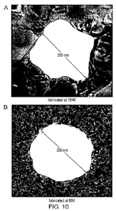
Figure 10 shows controlling the shape of sub-micrometer (nanometer) holes in a
nanocrystalline gold foil. Transmission electron micrographs of typical holes
in a gold foil
CA 03172576 2022- 9- 21
WO 2021/191307 21
PCT/EP2021/057628
produced by evaporation onto a silicon template (210 nm holes) at ambient
temperature (A) and
at 85K, achieved by liquid nitrogen cooling of the substrate (B). The gold was
evaporated at the
same rate (1 A/s) in both cases. Reducing the temperature reduces the gold
grain size by a
factor the order of 10x by reducing the surface diffusivity of the deposited
gold. This allows for
the formation of more regular and rounder holes.
Figures 11A to 11E illustrate the improvements of the present electron
microscopy supports by
detailing and comparing the defects in currently known supports.
Figure 12 shows scanning electron micrographs of a HexAuFoil grid, fully
fabricated on a holey
wafer, and still attached to the wafer. All micrographs are acquired at 300
tilt, with 30 kV
acceleration voltage using an Everhart-Thornley detector.
Figure 12A shows one full HexAuFoil grid that has a diameter of 3 mm and is
separated from
the neighbouring grids on the wafer. The darkest areas correspond to the
exposed silicon
surface of the templating wafer. Arrow 1 points to one of the four fiducial
markers on the grid,
which label each of the four quadrants. The grid also has two rim marks, which
are visible by
eye. The largest quadrant mark (arrow 2) is clear of foil, and this location
can be conveniently
used to perform electron microscope alignments and flux measurement. Arrow 3
points to the
thin gold foil connection strips between the grids which provide continuous
electrical contact for
electroplating. The dashed boxes indicate the magnified areas in Figures 12B,
12C, and 12D
(from top to bottom).
Figure 12B shows that each grid contains a center mark. The writing appears
mirrored by
design; when the grid is separated from the wafer and viewed from the flat
foil side, it will be
flipped to the correct orientation.
Figure 12C shows that each hexagon is 50 micrometres wide, and contains 8000-
9000 holes.
In designs with alternative pitches, this size hexagon might have 3000-5000
holes. For smaller
hexagons, the number of holes per hexagon is reduced in proportion to the open
area. The grid
bars are formed of electroplated gold, and are 10 micrometres wide and 10
micrometres thick in
this example. The preferred thickness is from 5 to 20 micrometers. The aspect
ratio of the bar
CA 03172576 2022- 9- 21
WO 2021/191307 22
PCT/EP2021/057628
(thickness/width) is preferably in the range from 0.25 to 4, and in most cases
0.5 to 2, with this
example equal to 1.
Figure 120 shows that each grid has a clear rim mark, which is also visible by
eye (requiring
dimensions of at least 0.2 mm). The radial direction from the center of the
grid toward the rim
mark is indicated with a line going across the middle of the hexagons. This
line is visible in the
electron microscope, and can be used, along with the other alignment features,
to map the
orientation of the grid in the microscope, relative to its orientation during
specimen preparation,
for example.
Figure 13 shows HexAuFoil grids with 200¨ 300 nm hole diameters. Figures 13A
and 13B
show scanning electron micrographs of two HexAuFoil gold foils, still attached
to the templating
silicon holey wafer via the sacrificial copper underlayer. Both micrographs
are acquired at 0 tilt,
with 30 kV acceleration voltage using an Everhart-Thornley detector. The scale
is set by the
center-to-center hole spacing, which is 600 nm for both. The foils in Figures
13A and 13B differ
only by the templating hole diameter, which is 300 nm for Figure 13A and 200
nm for Figure
13B, respectively. Discs of gold foil can be seen at the bottom of each hole
in the silicon wafer,
with a shadowing angle dependent on the viewing angle from the gold source
during electron
beam evaporation of the foil towards the given point on the wafer. If the
holes are insufficiently
deep, these discs can remain attached to the foil and obstruct the holes when
the foil is
released from the wafer. A depth of 500 nm is sufficient to avoid this for 200
¨ 300 nm holes
and 300 A thick copper and gold foils.
Figure 14 shows HexAuFoil grids released from the wafer post-fabrication.
Figure 14A shows a scanning electron micrograph (45 tilt, with 2 kV
acceleration voltage using
an Everhart-Thornley detector) of the bar side of the grid after release from
the wafer and
removal of the copper adhesion layer. The grid is clipped in a standard clip-
ring/clip holder used
for transmission electron microscopy.
Figure 14B shows a scanning electron micrograph (45 tilt, with 30 kV
acceleration voltage
using an Everhart-Thornley detector) of one of the hexagons on the same grid,
acquired from
the flat foil side of the grid, i.e. after the grid is flipped over relative
to its orientation in Figure
CA 03172576 2022- 9- 21
WO 2021/191307 23
PCT/EP2021/057628
14A. This is the side of the grid that was originally covered with the
sacrificial copper layer,
making contact to the silicon template. The holey foil spans each grid hexagon
and remains
intact.
Figure 14C shows a scanning electron micrograph (450 tilt, with 30 kV
acceleration voltage
using an Everhart-Thornley detector) of the holey gold foil demonstrates the
edge flatness of
each hole and surface flatness of the foil. These characteristics help with
the formation of a thin,
flat ice layer when the grids are used for cryoEM sample preparation.
Figure 140 shows a transmission electron micrograph of the suspended gold foil
on the grid
after release from the wafer, which can be used as a sample support for
transmission electron
microscopy. The spacing between the holes is 600 nm. The dashed box delineates
the area
magnified in Figure 14E.
Figure 14E shows a transmission electron micrograph of one hole in the gold
foil of the free-
standing HexAuFoil grid. The hole diameter is 300 nm as indicated. The edge
roughness is
limited by the grain size of the gold foil, in this case approximately 20 nm
for gold deposited at
85 ¨ 90 Kelvin substrate temperature. Dashed black circle is exactly round,
for comparison with
the edge of the hole.
Figure 14F shows in-plane movement statistics of gold nanoparticles in the
HexAuFoil grids
produced by the wafer-scale method (right) indicate the performance of these
grids in terms of
reducing specimen movement is equivalent to that of the HexAuFoil grids
produced by the small
scale method in the previous publication (Naydenova, Jia & Russo 2020) (left).
Detailed Description
The features disclosed in the foregoing description, or in the following
claims, or in the
accompanying drawings, expressed in their specific forms or in terms of a
means for performing
the disclosed function, or a method or process for obtaining the disclosed
results, as
appropriate, may, separately, or in any combination of such features, be
utilised for realising the
invention in diverse forms thereof.
CA 03172576 2022- 9- 21
WO 2021/191307 24
PCT/EP2021/057628
While the invention has been described in conjunction with the exemplary
embodiments
described above, many equivalent modifications and variations will be apparent
to those skilled
in the art when given this disclosure. Accordingly, the exemplary embodiments
of the invention
set forth above are considered to be illustrative and not limiting. Various
changes to the
described embodiments may be made without departing from the scope of the
invention.
For the avoidance of any doubt, any theoretical explanations provided herein
are provided for
the purposes of improving the understanding of a reader. The inventors are not
bound by any of
these theoretical explanations.
Any section headings used herein are for organizational purposes only and are
not to be
construed as limiting the subject matter described.
Throughout this specification, including the claims which follow, unless the
context requires
otherwise, the words "have", "comprise", and "include", and variations such as
"having",
"comprises", "comprising", and "including" will be understood to imply the
inclusion of a stated
integer or step or group of integers or steps but not the exclusion of any
other integer or step or
group of integers or steps.
It must be noted that, as used in the specification and the appended claims,
the singular forms
"a," "an," and "the" include plural referents unless the context clearly
dictates otherwise. Ranges
may be expressed herein as from "about" one particular value, and/or to
"about" another
particular value. When such a range is expressed, another embodiment includes
from the one
particular value and/or to the other particular value. Similarly, when values
are expressed as
approximations, by the use of the antecedent "about," it will be understood
that the particular
value forms another embodiment. The term "about" in relation to a numerical
value is optional
and means, for example, +/- 10%.
The words "preferred" and "preferably" are used herein refer to embodiments of
the invention
that may provide certain benefits under some circumstances. It is to be
appreciated, however,
that other embodiments may also be preferred under the same or different
circumstances. The
recitation of one or more preferred embodiments therefore does not mean or
imply that other
CA 03172576 2022- 9- 21
WO 2021/191307 25
PCT/EP2021/057628
embodiments are not useful, and is not intended to exclude other embodiments
from the scope
of the disclosure, or from the scope of the claims.
As used herein, the term "metallic" is used to refer to a material or
component (such as a foil)
displaying properties of a metal. In particular they display high electrical
and thermal
conductivity. In many cases electrical conductivity in metallic materials is
higher than 104 S/m.
Electron Microscopy Support
A support for electron microscopy is an apparatus which allows the carriage of
the sample to be
examined by electron microscopy into and out of the electron microscope. A
degree of
mechanical strength is provided to the support by a peripheral wall or rim
inside which is
typically arranged a mesh of members (such as grid bars). The sample to be
examined is
mounted onto the support within an area defined by the periphery of the grid
bars. In cryoEM,
the sample itself is suspended in a film (such as in a vitreous ice film)
which is suspended in the
holes or pores of a foil that is suspended between the grid bars. Foils are
also commonly
referred to as supporting films.
The foil part of the support typically has a mesh or "holey film" structure.
These foils are typically
described in the art with two numbers, for example "2/1" - this means a foil
with two micrometre
pores at a one micrometre spacing. Similarly, a foil designated 2/4 would have
holes or pores of
two micrometres, at a spacing of four micrometres, and so on. The term
"support" includes
instances where the foil is provided with and without a grid.
Example 1 - High Resolution cryoEM structural determination of DNA protection
during
starvation protein (DPS)
To demonstrate the use of movement-free specimen supports for high-resolution
cryoEM the
structure of the 220 kDa DNA protection during starvation protein (DPS) was
determined. DPS
was plunge frozen on grids with 280 A thick gold foil with 260 nm holes. The
average resolution
from an initial reconstruction from about 9 hours of automated data collection
on a modern
300 keV microscope, easily reached <2 A and the total particle displacement
was 0.86 A RMS
in 35 e-tA2 of irradiation. The absence of buckling also ensured no
significant rotation of the
CA 03172576 2022- 9- 21
WO 2021/191307 26
PCT/EP2021/057628
particles during imaging. In contrast to all previous single particle cryoEM
datasets to date,
maps reconstructed from each frame show that the first frame (1 e-/A2 or 3
MGy) contained the
most structural information and the quality (B-factor) of sequential frames
decays linearly with
dose/fluence. A linear decay in B-factor with dose is expected from studies of
radiation damage
in X-ray and electron crystallography, but has never previously been observed
for single particle
cryoEM due to movement at the onset of irradiation.
Example 2 - Gold foil characterisation
The mean linear intercept grain size of some gold foils fabricated as
described herein were
measured by TEM and found to be 100 10 A. This is approximately 20 times
smaller than the
grain size in gold foils fabricated under similar conditions but at room
temperature. The small
grain size allows for both thinner foils and smoother hole edges. The typical
edge roughness of
200 to 300 nm holes (deviation from a circular shape) is less than 10 nm.
Comparative Examples - Previous foils are unfit for purpose
The following examples illustrate the improvements of the present electron
microscopy supports
by detailing and comparing the defects in currently known supports.
Defect type 1: Malformed holes due to increased grain size due to increased
evaporation rate
The gold film shown in Figure 11A was evaporated at a rate of 6 A/s onto the
patterned
substrate held at about 90K. The sacrificial copper layer (not shown) was
evaporated at 27 A/s.
These evaporation rates resulted in malformed holes due to the increased grain
size. The hole
diameters vary between 50 and 250 nm. Compare with the foil in Figure 11D,
which was
produced by evaporation onto the same template at the same temperature, but at
a lower rate
(1 A/s for both copper and gold), and has the same thickness. In that foil,
the typical hole
deviation from roundness is 10 nm or less.
Defect type 2: Malformed holes due to increased grain size due to increased
evaporation
temperature are shown in Figure 10A.
Defect type 3: Malformed holes due to over-etching
CA 03172576 2022- 9- 21
WO 2021/191307 27
PCT/EP2021/057628
The gold foil shown in Figure 11B was evaporated in a way identical to the one
from
Figure 11E, onto the same substrate. The release (etching of the sacrificial
Cu layer in ferric
chloride) was 2 times slower for this film than for the one in Figure 11E (30
min vs 15 min). This
resulted in irregular enlargement of the holes (by about 50 nm) due to etching
of the gold by the
ferric chloride. The distance between holes (pitch) is 600 nm.
Defect type 4: Porosity
The gold foil shown in Figure 11C was manufactured by the method in Russo 2014
where the
gold evaporation is at room temperature. The foil thickness is 326 A, and the
holes are 2 pm in
diameter. This is thicker than the present foils. Due to the larger grain size
of about 200 nm the
foil remains porous at this thickness and is unstable. This was demonstrated
using in the paper
Russo 2014 which shows that even a 397 A thick foil becomes unstable due to
this porosity and
discontinuous metal foil. The typical pore dimensions are 200 nm long x 10 nm
wide and 30 to
40 / pm2.
Gold foils produced by the sputtering method in Janbroers et al. 2009 also
suffer from this
porosity, besides not being made from pure gold. The pores are clear in Fig.
1C and Fig. 5. This
is in contrast to the present foils which do not have such pores.
Although the data provided herein relates to gold, similar improvements are
expected to be
seen in materials having similar structural and electrical properties such as
transition metals,
aluminium, beryllium and degenerately doped silicon having a second element
selected from
boron, aluminium, phosphorus, and arsenic at a concentration of 1020 atoms/cm3
or higher
References
1. Ermantraut, E., Wohlfart, K. & Tichelaar, W. Perforated support foils with
pre-defined hole
size, shape and arrangement. Ultramicroscopy 74, 75-81 (1998).
2. Janbroers, S., de Kruijff, T. R., Xu, Q., Kooyman, P. J. & Zandbergen, H.
W. Preparation of
carbon-free TEM nnicrogrids by metal sputtering. Ultrannicroscopy 109, 1105-
1109 (2009).
3. Russo, C. J. & Passmore, L. A. Ultrastable gold substrates for electron
cryomicroscopy.
Science 346, 1377-1380 (2014).
CA 03172576 2022- 9- 21
WO 2021/191307 28
PCT/EP2021/057628
4. Russo, C. J. & Passmore, L. A. Ultrastable gold substrates: Properties of a
support for high-
resolution electron cryomicroscopy of biological specimens. Journal of
Structural Biology
193, 33-44 (2016).
5. Grant-Jacob, J. A. et al. Design and fabrication of a 3D-structured gold
film with nanopores
for local electric field enhancement in the pore. Nanotechnology 27, 65302
(2015).
6. Jia, P. et al. Large-area freestanding gold nanomembranes with nanoholes.
Materials
Horizons 6, 1005-1012 (2019).
7. Naydenova, K., Peet, M. J. & Russo, C. J. Multifunctional graphene supports
for electron
cryomicroscopy. Proceedings of the National Academy of Sciences 201904766
(2019)
doi:10.1073/pnas.1904766116.
CA 03172576 2022- 9- 21