Note: Descriptions are shown in the official language in which they were submitted.
1
STACK ALIGNMENT TECHNIQUES
FIELD
[0001] The embodiments provided herein generally relate to techniques that may
be used to
determine the alignment of substrates in a stack of substrates.
[0002] Embodiments are particularly appropriate in the manufacture and/or
testing of a device for the
manipulation of sub-beams of charged particles in a multi-beam charged
particle apparatus.
BACKGROUND
[0003] When manufacturing semiconductor integrated circuit (IC) chips,
undesired pattern defects,
as a consequence of, for example, optical effects and incidental particles,
inevitably occur on a
substrate (i.e. wafer) or a mask during the fabrication processes, thereby
reducing the yield.
Monitoring the extent of the undesired pattern defects is therefore an
important process in the
manufacture of IC chips. More generally, the inspection and/or measurement of
a surface of a
substrate, or other object/material, is an import process during and/or after
its manufacture.
[0004] Pattern inspection tools with a charged particle beam have been used to
inspect objects, for
example to detect pattern defects. These tools typically use electron
microscopy techniques, such as a
scanning electron microscope (SEM). In a SEM, a primary electron beam of
electrons at a relatively
high energy is targeted with a final deceleration step in order to land on a
sample at a relatively low
landing energy. The beam of electrons is focused as a probing spot on the
sample. The interactions
between the material structure at the probing spot and the landing electrons
from the beam of
electrons cause electrons to be emitted from the surface, such as secondary
electrons, backscattered
electrons or Auger electrons. The generated secondary electrons may be emitted
from the material
structure of the sample. By scanning the primary electron beam as the probing
spot over the sample
surface, secondary electrons can be emitted across the surface of the sample.
By collecting these
emitted secondary electrons from the sample surface, a pattern inspection tool
may obtain an image
representing characteristics of the material structure of the surface of the
sample.
[0005] Another application for a charged particle beam is lithography. The
charged particle beam
reacts with a resist layer on the surface of a substrate. A desired pattern in
the resist can be created by
controlling the locations on the resist layer that the charged particle beam
is directed towards.
A charged particle apparatus may be an apparatus for generating, illuminating,
projecting and/or
detecting one or more beams of charged particles. Within a charged particle
apparatus, a number of
devices are provided for manipulating one or more beams of charged particles.
Each
CA 03172893 2022- 9- 22
2928940-1
WO 2021/190976 2
PCT/EP2021/056519
device may comprise a stack of substrates. There is a general need to improve
the manufacturing and
testing of devices that comprise a stack of substrates.
SUMMARY
[0007] The embodiments provided herein disclose techniques for determining the
relative alignment
of substrates in a stack. Embodiments also include determining the relative
alignments of a stack of
substrate and a PCB support of the stack.
[0008] According to a first aspect of the invention, there is provided a
substrate stack comprising a
plurality of substrates, wherein: each substrate in the substrate stack
comprises at least one alignment
opening set; the at least one alignment opening set in each substrate is
aligned for a light beam to pass
through corresponding alignment openings in each substrate; and each substrate
comprises at least one
alignment opening that has a smaller diameter than the corresponding alignment
openings in the other
substrates.
[0009] According to a second aspect of the invention, there is provided a
method for determining the
alignment of substrates in a substrate stack that comprises a plurality of
substrates, the method
comprising: determining the positions of a plurality of light beams that have
passed through a
respective plurality of alignment openings defined in each substrate in the
substrate stack; and
determining the relative x, y, and Rz alignments of at least two substrates in
the substrate stack in
dependence on the determined positions; wherein: for each light beam path
through the substrate
stack, the alignment opening of one of the substrates on the light beam path
has a smaller diameter
than all of one or more other alignment openings of respective one or more
other substrates on the
light beam path; and for each one of at least two of the plurality of light
beam paths, a different one of
the substrates on thc light beam path has an alignment opening with a smaller
diameter than all of one
or more other alignment openings of respective one or more other substrates on
the light beam path
such that, for each one of at least two substrates in the substrate stack,
there are one or more light
beams paths with positions that are indicative of the position of only said
one substrate.
[0010] According to a third aspect of the invention, there is provided a
computing system configured
to determine the alignment of substrates in a substrate stack by performing
the method according to
the second aspect.
[0011] According to a fourth aspect of the invention, there is provided a tool
for obtaining data
indicative of light beam locations, the tool comprising: a stack holder
configured to hold a substrate
stack according to the first aspect; an illuminator configured to illuminate
at least part of a surface of
the substrate stack; and a light detector configured to generate data
indicative of the light beam
locations in dependence on a plurality of light beams that have passed through
the substrate stack.
[0012] According to a fifth aspect of the invention, there is provided a
system comprising the tool
according to the fourth aspect and the computing system according to the third
aspect.
CA 03172893 2022- 9- 22
3
[0013] According to a sixth aspect of the invention, there is provided a
method for determining the
alignment of substrates in a substrate stack, the substrate stack having at
least two substrates, wherein
in each of the substrates there are a plurality of alignment openings that
align with corresponding
alignment openings in the other substrates of the substrate stack such that
there is a through passage
through the substrate stack associated with each alignment opening in each
substrate, the method
comprising: determining the relative positions of a plurality of light beams,
each light beam having
passed along a light path through the substrate stack via a respective through
passage; and
determining the relative x, y, and Rz alignments of the substrates in the
substrate stack in dependence
on the determined positions; wherein: the alignment opening of one of the
substrates that defines the
through passage for a corresponding light path through the through passage has
a smaller diameter
than the other alignment openings that define the through passage; and for
each light path a different
substrate in the substrate stack has an diameter with a smaller diameter than
the other alignment
openings that define the corresponding through passage in the substrate stack.
[0014] According to a seventh aspect of the invention, there is provided a
substrate stack of
substrates comprising beam manipulators, the substrate stack having at least
two substrates, wherein
in each substrate there are a plurality of alignment openings that align with
corresponding alignment
openings in the other substrates of the substrate stack such that there is a
through passage through the
substrate stack associated with each alignment opening in each substrate,
wherein each of the plurality
of through passages is for the passage of a light beam and the light beams are
suitable for determining
the relative x, y, and Rz alignments of the substrates in the substrate stack;
wherein: the alignment
opening of one of the substrates, that defines the through passage fora
corresponding light path
through the through passage, has a smaller diameter than the other alignment
openings that define the
through passage; and a different substrate in the substrate stack has an
alignment opening with a
smaller diameter than the other alignment openings that define the
corresponding through passage in
the substrate stack.
[0015] According to an eighth aspect of the invention, there is provided a
combination of a printed
circuit board, PCB, and the substrate stack as described herein, the substrate
stack being provided on
the PCB, wherein: in the PCB is defined an opening configured to be aligned
with the through
passage in the substrate stack for interacting with a stack light source; and
a surface of the PCB
comprises a plurality of alignment structures configured to interact with a
PCB light source.
[0016] According to a ninth aspect of the invention, there is provided a
combination of a printed
circuit board, PCB, and substrate stack in which is defined a plurality of
through passages for beam
path openings, the substrate stack being provided on the PCB, wherein in a
surface of the PCB is a
plurality of alignment structures configured to interact with a light source
for enabling the alignment
of the PCB to be determined.
[0017] According to a tenth aspect of the invention, there is provided a
method for determining the
relative alignments of a substrate stack and a printed circuit board, PCB,
wherein the substrate stack is
CA 03172893 2022- 9- 22
WO 2021/190976 4
PCT/EP2021/056519
provided on the PCB, the method comprising: determining the positions of a
first plurality of light
beams that have passed through both a respective plurality of openings through
the substrate stack and
at least one opening in the PCB; determining the positions of a second
plurality of light beams that are
dependent on a plurality of PCB alignment structures; and determining the
relative x, y, and Rz
alignments of the substrate stack and the PCB in dependence on the determined
positions of the first
and second plurality of light beams.
[0018] According to a eleventh aspect of the invention, there is provided a
computing system
configured to determine the alignment of a PCB and a substrate stack by
performing the
method according to the tenth aspect.
[0019] Other advantages of the present invention will become apparent from the
following
description taken in conjunction with the accompanying drawings wherein are
set forth, by way of
illustration and example, certain embodiments of the present invention.
BRIEF DESCRIPTION OF FIGURES
[0020] The above and other aspects of the present disclosure will become more
apparent from the
description of exemplary embodiments, taken in conjunction with the
accompanying drawings.
[0021] FIG. 1 is a schematic diagram illustrating an exemplary charged
particle beam inspection
apparatus.
[0022] FIG. 2 is a schematic diagram illustrating an exemplary multi-beam
apparatus that is part of
the exemplary charged particle beam inspection apparatus of FIG. 1.
[0023] FIG. 3 is a schematic diagram of exemplary multi-beam apparatus
illustrating an exemplary
configuration of source conversion unit of the exemplary charged particle beam
inspection apparatus
of FIG. 1.
[0024] FIG. 4 is schematic diagram showing a cross-section through a stack of
two substrates
according to an embodiment.
[0025] FIG. 5 shows four different relative locations of light spots according
to embodiments.
[0026] FIGS. 6A and 6B show configurations of alignment opening sets according
to an
embodiment.
DESCRIPTION OF EMBODIMENTS
[0027] Reference will now be made in detail to exemplary embodiments, examples
of which arc
illustrated in the accompanying drawings. The following description refers to
the accompanying
drawings in which the same numbers in different drawings represent the same or
similar elements
unless otherwise represented. The implementations set forth in the following
description of
exemplary embodiments do not represent all implementations consistent with the
invention. Instead,
CA 03172893 2022- 9- 22
WO 2021/190976 5
PCT/EP2021/056519
they are merely examples of apparatuses and methods consistent with aspects
related to the invention
as recited in the appended claims.
[0028] The reduction of the physical size of devices, and enhancement of the
computing power of
electronic devices, can be accomplished by significantly increasing the
packing density of circuit
components such as transistors, capacitors, diodes, etc. on an IC chip. This
has been enabled by
increased resolution enabling yet smaller structures to be made. For example,
an IC chip of a smart
phone, which is the size of a thumbnail and available in, or earlier than,
2019, may include over 2
billion transistors, the size of each transistor being less than 1/1000th of a
human hair. Thus, it is not
surprising that semiconductor IC manufacturing is a complex and time-consuming
process, with
hundreds of individual steps. Errors in even one step have the potential to
dramatically affect the
functioning of the final product. Just one "killer defect" can cause device
failure. The goal of the
manufacturing process is to improve the overall yield of the process. For
example, to obtain a 75%
yield for a 50-step process (where a step can indicate the number of layers
formed on a wafer), each
individual step must have a yield greater than 99.4%,. If an individual step
has a yield of 95%, the
overall process yield would be as low as 7-8%.
[0029] While high process yield is desirable in an IC chip manufacturing
facility, maintaining a high
substrate (i.e. wafer) throughput, defined as the number of substrates
processed per hour, is also
essential. High process yield and high substrate throughput can be impacted by
the presence of a
defect. This is especially if operator intervention is required for reviewing
the defects. Thus, high
throughput detection and identification of micro and nano-scale defects by
inspection tools (such as a
Scanning Electron Microscope ('SEM')) is essential for maintaining high yield
and low cost.
[0030] A SEM comprises an scanning device and a detector apparatus. The
scanning device
comprises an illumination apparatus that comprises an electron source, for
generating primary
electrons, and a projection apparatus for scanning a sample, such as a
substrate, with one or more
focused beams of primary electrons. The primary electrons interact with the
sample and generate
secondary electrons. The detection apparatus captures the secondary electrons
from the sample as the
sample is scanned so that the SEM can create an image of the scanned area of
the sample. For high
throughput inspection, some of the inspection apparatuses use multiple focused
beams, i.e. a multi-
beam, of primary electrons. The component beams of the multi-beam may be
referred to as sub-
beams or beamlets. A multi-beam can scan different parts of a sample
simultaneously. A multi-beam
inspection apparatus can therefore inspect a sample at a much higher speed
than a single-beam
inspection apparatus.
[0031] In a multi-beam inspection apparatus, the paths of some of the primary
electron beams are
displaced away from the central axis, i.e. a mid-point of the primary electron
optical axis, of the
scanning device. To ensure all the electron beams arrive at the sample surface
with substantially the
same angle of incidence, and/or with a desired pitch and/or at a desired
locations on the sample
surface, sub-beam paths with a greater radial distance from the central axis
need to be manipulated to
CA 03172893 2022- 9- 22
WO 2021/190976 6
PCT/EP2021/056519
move through a greater angle than the sub-beam paths with paths closer to the
central axis. This
stronger manipulation may cause aberrations which result in blurry and out-of-
focus images of the
sample substrate. In particular, for sub-beam paths that are not on the
central axis, the aberrations in
the sub-beams may increase with the radial displacement from the central axis
because the
manipulators of these sub-beam paths are required to operate at larger
voltages. Such aberrations may
remain associated with the secondary electrons when they are detected. Such
aberrations therefore
degrade the quality of images that are created during inspection.
100321 An implementation of a known multi-beam inspection apparatus is
described below.
[0033] The figures are schematic. Relative dimensions of components in
drawings are therefore
exaggerated for clarity. Within the following description of drawings the same
or like reference
numbers refer to the same or like components or entities, and only the
differences with respect to the
individual embodiments are described. While the description and drawings are
directed to an
electron-optical apparatus, it is appreciated that the embodiments are not
used to limit the present
disclosure to specific charged particles. References to electrons throughout
the present document may
therefore be more generally be considered to be references to charged
particles, with the charged
particles not necessarily being electrons.
100341 Reference is now made to FIG. 1, which is a schematic diagram
illustrating an exemplary
charged particle beam inspection apparatus 100. The charged particle beam
inspection apparatus 100
of Fig. 1 includes a main chamber 10, a load lock chamber 20, an electron beam
tool 40, an equipment
front end module (EFEM) 30 and a controller 50. Electron beam tool 40 is
located within main
chamber 10.
[0035] EFEM 30 includes a first loading port 30a and a second loading port
30b. EFEM 30 may
include additional loading port(s), First loading port 30a and second loading
port 30b may, for
example, receive substrate front opening unified pods (FOUPs) that contain
substrates (e.g.,
semiconductor substrates or substrates made of other material(s)) or samples
to be inspected
(substrates, wafers and samples are collectively referred to as "samples"
hereafter). One or more
robot arms (not shown) in EFEM 30 transport the samples to load lock chamber
20.
[0036] Load lock chamber 20 is used to remove the gas around a sample. This
creates a vacuum that
is a local gas pressure lower than the pressure in the surrounding
environment. The load lock
chamber 20 may be connected to a load lock vacuum pump system (not shown),
which removes gas
molecules in the load lock chamber 20. The operation of the load lock vacuum
pump system enables
the load lock chamber to reach a first pressure below the atmospheric
pressure. After reaching the
first pressure, one or more robot arms (not shown) transport the sample from
load lock chamber 20 to
main chamber 10. Main chamber 10 is connected to a main chamber vacuum pump
system (not
shown). The main chamber vacuum pump system removes gas molecules in main
chamber 10 so that
the pressure around the sample reaches a second pressure lower than the first
pressure. After reaching
the second pressure, the sample is transported to the electron beam tool by
which it may be inspected.
CA 03172893 2022- 9- 22
WO 2021/190976 7
PCT/EP2021/056519
An electron beam tool 40 may comprise either a single beam or a multi-beam
electron-optical
apparatus.
[0037] Controller 50 is electronically connected to electron beam tool 40.
Controller 50 may be a
processor (such as a computer) configured to control the charged particle beam
inspection apparatus
100. Controller 50 may also include a processing circuitry configured to
execute various signal and
image processing functions. While controller 50 is shown in FIG. 1 as being
outside of the structure
that includes main chamber 10, load lock chamber 20, and EFEM 30, it is
appreciated that controller
50 may be part of the structure. The controller 50 may be located in one of
the component elements
of the charged particle beam inspection apparatus or it can be distributed
over at least two of the
component elements. While the present disclosure provides examples of main
chamber 10 housing an
electron beam inspection tool, it should be noted that aspects of the
disclosure in their broadest sense
are not limited to a chamber housing an electron beam inspection tool. Rather,
it is appreciated that
the foregoing principles may also be applied to other tools and other
arrangements of apparatus, that
operate under the second pressure.
100381 Reference is now made to FIG. 2, which is a schematic diagram
illustrating an exemplary
electron beam tool 40 including a multi-beam inspection tool that is part of
the exemplary charged
particle beam inspection apparatus 100 of FIG. 1. Multi-beam electron beam
tool 40 (also referred to
herein as apparatus 40) comprises an electron source 201, a gun aperture plate
271, a condenser lens
210, a source conversion unit 220, a primary projection apparatus 230, a
motorized stage 209, and a
sample holder 207. The electron source 201, a gun aperture plate 271, a
condenser lens 210, a source
conversion unit 220 are the components of an illumination apparatus comprised
by the multi-beam
electron beam tool 40. The sample holder 207 is supported by motorized stage
209 so as to hold a
sample 208 (e.g., a substrate or a mask) for inspection. Multi-beam electron
beam tool 40 may
further comprise a secondary projection apparatus 250 and an associated
electron detection device
240. Primary projection apparatus 230 may comprise an objective lens 23L
Electron detection
device 240 may comprise a plurality of detection elements 241, 242, and 243. A
beam separator 233
and a deflection scanning unit 232 may be positioned inside primary projection
apparatus 230.
[0039] The components that are used to generate a primary beam may be aligned
with a primary
electron-optical axis of the apparatus 40. These components can include: the
electron source 201,
gun aperture plate 271, condenser lens 210, source conversion unit 220, beam
separator 233,
deflection scanning unit 232, and primary projection apparatus 230. Secondary
projection apparatus
250 and its associated electron detection device 240 may be aligned with a
secondary electron-optical
axis 251 of apparatus 40.
[0040] The primary electron-optical axis 204 is comprised by the electron-
optical axis of the of the
part of electron beam tool 40 that is the illumination apparatus. The
secondary electron-optical axis
251 is the electron-optical axis of the of the part of electron beam tool 40
that is a detection apparatus.
The primary electron-optical axis 204 may also be referred to herein as the
primary optical axis (to aid
CA 03172893 2022- 9- 22
WO 2021/190976 8
PCT/EP2021/056519
ease of reference) or charged particle optical axis. The secondary electron-
optical axis 251 may also
be referred to herein as the secondary optical axis or the secondary charged
particle optical axis.
[0041] Electron source 201 may comprise a cathode (not shown) and an extractor
or anode (not
shown). During operation, electron source 201 is configured to emit electrons
as primary electrons
from the cathode. The primary electrons are extracted or accelerated by the
extractor and/or the anode
to form a primary electron beam 202 that forms a primary beam crossover
(virtual or real) 203.
Primary electron beam 202 may be visualized as bcing emitted from primary beam
crossover 203.
[0042] In this arrangement a primary electron beam, by the time it reaches the
sample, and preferably
before it reaches the projection apparatus, is a multi-beam. Such a multi-beam
can be generated from
the primary electron beam in a number of different ways. For example, the
multi-beam may be
generated by a multi-beam array located before the cross-over, a multi-beam
array located in the
source conversion unit 220, or a multi-beam array located at any point in
between these locations. A
multi-beam array may comprise a plurality of electron beam manipulating
elements arranged in an
array across the beam path. Each manipulating element may influence the
primary electron beam to
generate a sub-beam. Thus the multi-beam array interacts with an incident
primary beam path to
generate a multi-beam path down-beam of the multi-beam array.
[0043] Gun aperture plate 271, in operation, is configured to block off
peripheral electrons of
primary electron beam 202 to reduce Coulomb effect. The Coulomb effect may
enlarge the size of
each of probe spots 221, 222, and 223 of primary sub-beams 211, 212, 213, and
therefore deteriorate
inspection resolution. A gun aperture plate 271 may also be referred to as a
coulomb aperture array.
[0044] Condenser lens 210 is configured to focus primary electron beam 202.
Condenser lens 210
may be designed to focus primary electron beam 202 to become a parallel beam
and be normally
incident onto source conversion unit 220. Condenser lens 210 may be a movable
condenser lens that
may be configured so that the position of its first principle plane is
movable. The movable condenser
lens may be configured to be magnetic. Condenser lens 210 may be an anti-
rotation condenser lens
and/or it may be movable.
[0045] Source conversion unit 220 may comprise an image-forming element array,
an aberration
compensator array, a beam-limit aperture array, and a pre-bending micro-
deflector array. The pre-
bending micro-deflector array may deflect a plurality of primary sub-beams
211, 212, 213 of primary
electron beam 202 to normally enter the beam-limit aperture array, the image-
forming element array,
and an aberration compensator array. In this arrangement, the image-forming
element array may
function as a multi-beam array to generate the plurality of sub-beams in the
multi-beam path, i.e.
primary sub-beams 211, 212, 211 The image forming array may comprise a
plurality electron beam
manipulators such as micro-deflectors micro-lenses (or a combination of both)
to influence the
plurality of primary sub-beams 211, 212, 213 of primary electron beam 202 and
to form a plurality of
parallel images (virtual or real) of primary beam crossover 203, one for each
of the primary sub-
beams 211, 212, and 213. The aberration compensator array may comprise a field
curvature
CA 03172893 2022- 9- 22
WO 2021/190976 9
PCT/EP2021/056519
compensator array (not shown) and an astigmatism compensator array (not
shown). The field
curvature compensator array may comprise a plurality of micro-lenses to
compensate field curvature
aberrations of the primary sub-beams 211, 212, and 213. The astigmatism
compensator array may
comprise a plurality of micro-stigmators to compensate astigmatism aberrations
of the primary sub-
beams 211, 212, and 213. The beam-limit aperture array may be configured to
limit diameters of
individual primary sub-beams 211, 212, and 213. FIG. 2 shows three primary sub-
beams 211, 212,
and 213 as an example, and it should be understood that source conversion unit
220 may be
configured to form any number of primary sub-beams. Controller 50 may be
connected to various
parts of charged particle beam inspection apparatus 100 of FIG. 1, such as
source conversion unit
220, electron detection device 240, primary projection apparatus 230, or
motorized stage 209. As
explained in further detail below, controller 50 may perform various image and
signal processing
functions. Controller 50 may also generate various control signals to govern
operations of the
charged particle beam inspection apparatus, including the charged particle
multi-beam apparatus.
[0046] Condenser lens 210 may further be configured to adjust electric
currents of primary sub-
beams 211, 212, 213 down-beam of source conversion unit 220 by varying the
focusing power of
condenser lens 210. Alternatively, or additionally, the electric currents of
the primary sub-beams 211,
212, 213 may be changed by altering the radial sizes of beam-limit apertures
within the beam-limit
aperture array corresponding to the individual primary sub-beams. The electric
currents may be
changed by both altering the radial sizes of beam-limit apertures and the
focusing power of condenser
lens 210. If the condenser lens is moveable and magnetic, off-axis sub-beams
212 and 213 may result
that illuminate source conversion unit 220 with rotation angles. The rotation
angles change with the
focusing power or the position of the first principal plane of the movable
condenser lens. A
condenser lens 210 that is an anti-rotation condenser lens may be configured
to keep the rotation
angles unchanged while the focusing power of condenser lens 210 is changed.
Such a condenser lens
210 that is also movable, may cause the rotation angles not change when the
focusing power of the
condenser lens 210 and the position of its first principal plane are varied.
[0047] Objective lens 231 may be configured to focus sub-beams 211, 212, and
213 onto a sample
208 for inspection and may form three probe spots 221, 222, and 223 on the
surface of sample 208.
[0048] Beam separator 233 may be, for example, a Wien filter comprising an
electrostatic deflector
generating an electrostatic dipole field and a magnetic dipole field (not
shown in FIG. 2). In
operation, beam separator 233 may be configured to exert an electrostatic
force by electrostatic dipole
field on individual electrons of primary sub-beams 211, 212, and 213. The
electrostatic force is equal
in magnitude but opposite in direction to the magnetic force exerted by
magnetic dipole field of beam
separator 233 on the individual electrons. Primary sub-beams 211, 212, and 213
may therefore pass at
least substantially straight through beam separator 233 with at least
substantially zero deflection
angles.
CA 03172893 2022- 9- 22
WO 2021/190976 10
PCT/EP2021/056519
[0049] Deflection scanning unit 232, in operation, is configured to deflect
primary sub-beams 211,
212, and 213 to scan probe spots 221, 222, and 223 across individual scanning
areas in a section of
the surface of sample 208. In response to incidence of primary sub-beams 211,
212, and 213 or probe
spots 221, 222, and 223 on sample 208, electrons are generated from the sample
208 which include
secondary electrons and backscattered electrons. The secondary electrons
propagate in three
secondary electron beams 261, 262, and 263. The secondary electron beams 261,
262, and 263
typically have secondary electrons (having electron energy
50eV) and may also have at least some
of the backscattered electrons (having electron energy between 50eV and the
landing energy of
primary sub-beams 211, 212, and 213). The beam separator 233 is arranged to
deflect the path of the
secondary electron beams 261, 262, and 263 towards the secondary projection
apparatus 250. The
secondary projection apparatus 250 subsequently focuses the path of secondary
electron beams 261,
262, and 263 onto a plurality of detection regions 241, 242, and 243 of
electron detection device 240.
The detection regions may be the separate detection elements 241, 242, and 243
that are arranged to
detect corresponding secondary electron beams 261, 262, and 263. The detection
regions generate
corresponding signals which are sent to controller 50 or a signal processing
system (not shown), e.g.
to construct images of the corresponding scanned areas of sample 208.
[0050] The detection elements 241, 242, and 243 may detect the corresponding
secondary electron
beams 261, 262, and 263. On incidence of secondary electron beams with the
detection elements 241,
242 and 243, the elements may generate corresponding intensity signal outputs
(not shown). The
outputs may be directed to an image processing system (e.g., controller 50).
Each detection element
241, 242, and 243 may comprise one or more pixels. The intensity signal output
of a detection
element may be a sum of signals generated by all the pixels within the
detection element.
[0051] The controller 50 may comprise image processing system that includes an
image acquirer (not
shown) and a storage device (not shown). For example, the controller may
comprise a processor,
computer, server, mainframe host, terminals, personal computer, any kind of
mobile computing
devices, and the like, or a combination thereof. The image acquirer may
comprise at least part of the
processing function of the controller. Thus the image acquirer may comprise at
least one or more
processors. The image acquirer may be communicatively coupled to an electron
detection device 240
of the apparatus 40 permitting signal communication, such as an electrical
conductor, optical fiber
cable, portable storage media, IR, Bluetooth, internet, wireless network,
wireless radio, among others,
or a combination thereof. The image acquirer may receive a signal from
electron detection device
240, may process the data comprised in the signal and may construct an image
therefrom. The image
acquirer may thus acquire images of sample 208. The image acquirer may also
perform various post-
processing functions, such as generating contours, superimposing indicators on
an acquired image,
and the like. The image acquirer may be configured to perform adjustments of
brightness and
contrast, etc. of acquired images. The storage may be a storage medium such as
a hard disk, flash
CA 03172893 2022- 9- 22
WO 2021/190976 11
PCT/EP2021/056519
drive, cloud storage, random access memory (RAM), other types of computer
readable memory, and
the like. The storage may be coupled with the image acquirer and may be used
for saving scanned
raw image data as original images, and post-processed images.
[0052] The image acquirer may acquire one or more images of a sample based on
an imaging signal
received from the electron detection device 240. An imaging signal may
correspond to a scanning
operation for conducting charged particle imaging. An acquired image may be a
single image
comprising a plurality of imaging areas. The single image may be stored in the
storage. The single
image may be an original image that may be divided into a plurality of
regions. Each of the regions
may comprise one imaging area containing a feature of sample 208. The acquired
images may
comprise multiple images of a single imaging area of sample 208 sampled
multiple times over a time
period. The multiple images may be stored in the storage. The controller 50
may be configured to
perform image processing steps with the multiple images of the same location
of sample 208.
[0053] The controller 50 may include measurement circuitry (e.g., analog-to-
digital converters) to
obtain a distribution of the detected secondary electrons. The electron
distribution data, collected
during a detection time window, can be used in combination with corresponding
scan path data of
each of primary sub-beams 211, 212, and 213 incident on the sample surface, to
reconstruct images of
the sample structures under inspection. The reconstructed images can be used
to reveal various
features of the internal or external structures of sample 208. The
reconstructed images can thereby be
used to reveal any defects that may exist in the sample.
[0054] The controller 50 may control motorized stage 209 to move sample 208
during inspection of
sample 208. The controller 50 may enable motorized stage 209 to move sample
208 in a direction,
preferably continuously, for example at a constant speed, at least during
sample inspection. The
controller 50 may control movement of the motorized stage 209 so that it
changes the speed of the
movement of the sample 208 dependent on various parameters. For example, the
controller may
control the stage speed (including its direction) depending on the
characteristics of the inspection
steps of scanning process.
[0055] Although FIG. 2 shows that apparatus 40 uses three primary electron sub-
beams, it is
appreciated that apparatus 40 may use two or more number of primary electron
sub-beams. The
present disclosure does not limit the number of primary electron beams used in
apparatus 40.
[0056] Reference is now made to FIG. 3, which is a schematic diagram of
exemplary multi-beam
apparatus illustrating an exemplary configuration of source conversion unit of
the exemplary charged
particle beam inspection apparatus of FIG. 1. The apparatus 300 may comprise
an election source
301, a pre-sub-beam-forming aperture array 372, a condenser lens 310 (similar
to condenser lens 210
of FIG. 2), a source conversion unit 320, an objective lens 331 (similar to
objective lens 231 of FIG.
2), and a sample 308 (similar to sample 208 of FIG. 2). The election source
301, a pre-sub-beam-
forming aperture array 372, a condenser lens 310 may be the components of an
illumination apparatus
comprised by the apparatus 300. The source conversion unit 320, an objective
lens 331 may the
CA 03172893 2022- 9- 22
WO 2021/190976 12
PCT/EP2021/056519
components of a projection apparatus comprised by the apparatus 300. The
source conversion unit
320 may be similar to source conversion unit 220 of FIG. 2 in which the image-
forming element
array of FIG. 2 is image-forming element array 322, the aberration compensator
array of FIG. 2 is
aberration compensator array 324, the beam-limit aperture array of FIG. 2 is
beam-limit aperture
array 321, and the pre-bending micro-deflector array of FIG. 2 is pre-bending
micro-deflector array
323. The election source 301, the pre-sub-beam-forming aperture array 372, the
condenser lens 310,
the source conversion unit 320, and the objective lens 331 are aligned with a
primary electron-optical
axis 304 of the apparatus. The electron source 301 generates a primary-
electron beam 302 generally
along the primary electron-optical axis 304 and with a source crossover
(virtual or real) 301S. The
pre-sub-beam-forming aperture array 372 cuts the peripheral electrons of
primary electron beam 302
to reduce a consequential Coulomb effect. The Coulomb effect is a source of
aberration to the sub-
beams due to interaction between electrons in different sub-beam paths.
Primary-electron beam 302
may be trimmed into a specified number of sub-beams, such as three sub-beams
311, 312 and 313, by
pre-sub-beam-forming aperture array 372 of a pre-sub-beam-forming mechanism.
Although three
sub-beams and their paths are referred to in the previous and following
description, it should be
understood that the description is intended to apply an apparatus, tool, or
system with any number of
sub-beams.
[0057] The source conversion unit 320 may include a beamlet-limit aperture
array 321 with beam-
limit apertures configured to limit the sub-beams 311, 312, and 313 of the
primary electron beam 302.
The source conversion unit 320 may also include an image-forming element array
322 with image-
forming micro-deflectors, 3221, 3222, and 3223. There is a respective micro-
deflector associated
with the path of each sub-beam. The micro-deflectors 322_1, 322_2, and 322_3
are configured to
deflect the paths of the sub-beams 311, 312, and 313 towards the electron-
optical axis 304. The
deflected sub-beams 311, 312 and 313 form virtual images of source crossover
301S. The virtual
images are projected onto the sample 30g by the objective lens 331 and form
probe spots thereon,
which are the three probe spots, 391, 392, and 393. Each probe spot
corresponds to the location of
incidence of a sub-beam path on the sample surface. The source conversion unit
320 may further
comprise an aberration compensator array 324 configured to compensate
aberrations of each of the
sub-beams. The aberrations in each sub-beam are typically present on the probe
spots, 391, 392, and
393 that would be formed a sample surface. The aberration compensator array
324 may include a
field curvature compensator array (not shown) with micro-lenses. The field
curvature compensator
and micro-lenses are configured to compensate the sub-beams for field
curvature aberrations evident
in the probe spots, 391, 392, and 393. The aberration compensator array 324
may include an
astigmatism compensator array (not shown) with micro-stigmators. The micro-
stigmators are
controlled to operate on the sub-beams to compensate astigmatism aberrations
that are otherwise
present in the probe spots, 391, 392, and 393.
CA 03172893 2022- 9- 22
WO 2021/190976 13
PCT/EP2021/056519
[0058] The source conversion unit 320 may further comprise a pre-bending micro-
deflector array
323 with pre-bending micro-deflectors 323_i, 323_2, and 323_3 to bend the sub-
beams 311, 312, and
313 respectively. The pre-bending micro-deflectors 323_i, 323_2, and 323_3 may
bend the path of
the sub-beams onto the beamlet-limit aperture array 321. The sub-beam path of
the incident on
beamlet-limit aperture array 321 may be orthogonal to the plane of orientation
of the beamlet-limit
aperture array 321. The condenser lens 310 may direct the path of the sub-
beams onto the beamlet-
limit aperture array 321. The condenser lens 310 may focus the three sub-beams
311, 312, and 313 to
become parallel beams along primary electron-optical axis 304, so that it is
perpendicularly incident
onto source conversion unit 320, which may correspond to the beamlet-limit
aperture array 321.
[0059] The image-forming element array 322, the aberration compensator array
324, and the pre-
bending micro-deflector array 323 may comprise multiple layers of sub-beam
manipulating devices,
some of which may be in the form or arrays, for example: micro-deflectors,
micro-lenses, or micro-
stigmators.
[0060] In source the conversion unit 320, the sub-beams 311, 312 and 313 of
the primary electron
beam 302 arc respectively deflected by the micro-deflectors 322_i, 322_2 and
322_3 of image-
forming element array 322 towards the primary electron-optical axis 304. It
should be understood
that the sub-beam 311 path may already correspond to the electron-optical axis
304 prior to reaching
micro-deflector 322_i, accordingly the sub-beam 311 path may not be deflected
by micro-deflector
322_i.
[0061] The objective lens 331 focuses the sub-beams onto the surface of the
sample 308, i.e., it
projects the three virtual images onto the sample surface. The three images
formed by three sub-
beams 311 to 313 on the sample surface form three probe spots 391, 392 and 393
thereon. The
deflection angles of sub-beams 311 to 313 are adjusted by the objective lens
311 to reduce the off-axis
aberrations of three probe spots 391-393. The three deflected sub-beams
consequently pass through
or approach the front focal point of objective lens 331.
[0062] At least some of the above-described components in FIG. 2 and FIG. 3
may individually, or
in combination with each other, be referred to as a manipulator array, or
manipulator, because they
manipulate one or more beams, or sub-beams, of charged particles.
100631 The above described multi-beam inspection tool comprises a multi-beam
charged particle
apparatus, that may be referred to as a multi-beam charged particle optical
apparatus or a multi-beam
charged particle system, with a single source of charged particles. The multi-
beam charged particle
apparatus comprises an illumination apparatus and a projection apparatus. The
illumination apparatus
may generate a multi-beam of charged particles from the beam of electrons from
the source. The
projection apparatus projects a multi-beam of charged particles towards a
sample. At least part of the
surface of a sample is scanned with the multi-beam of charged particles.
[0064] The multi-beam charged particle apparatus may comprise one or more beam
manipulators. In
a single beam charged particle apparatus, there may be a beam manipulator for
manipulating the path
CA 03172893 2022- 9- 22
WO 2021/190976 14
PCT/EP2021/056519
of the beam. In a multi-beam charged particle apparatus, there may be an array
of beam manipulators,
i.e. a manipulator array, for manipulating the sub-beams of the multi-beam.
Each beam manipulator
may be, for example, a MEMS device or any type of other device/structure for
manipulating a
charged particle path. Each beam manipulator may comprise one or more
substrates. There may be
an opening through each beam manipulator for a sub-beam path through the beam
manipulator. The
periphery of a through-passage defined by the opening may feature one or more
electrodes. Each
beam manipulator be configured to manipulate, such as lens (e.g. focus) and/or
deflect, a sub-beam
path through its opening. The beam manipulators may be provided in an N by M
array. N may be,
for example, between 2 and 20, such as 5. M may be, for example, between 2 and
20, such as 5.
However, N and M may have any values and each of N and M may be several
thousand.
[0065] A manipulator array, that is an array of beam manipulators, may be
formed as a stack of
substrates, referred to as a substrate stack. Each substrate in the substrate
stack may comprise a
plurality of openings, i.e. holes, for providing the sub-beam paths through
the substrate stack. The
plurality of openings may be referred to as beam path openings. Each beam
manipulator in the
manipulator array may be constructed by securing, e.g. bonding together, two
or more substrate sets,
with each substrate set being substantially directly before and/or after
another substrate set along the
beam path. Each substrate set may comprise one or more substrates.
[0066] The performance of each beam manipulator is dependent on the relative
alignment of
substrates that arc bonded together to form the beam manipulator. In
particular, a substantial
misalignment between corresponding beam path openings in different sets of
substrates will distort, or
in a severe case prevent, the path of one or more of the sub-beams through the
substrate stack.
[0067] Embodiments provide techniques for determining the relative alignment
of the sets of
substrates that are secured together. Embodiments are described below with
reference to a plurality of
sets of substrates being secured together to form a manipulator array that
comprises an array of beam
manipulators. However, embodiments also include a plurality of sets of
substrates being secured
together to form a single beam manipulator. Embodiments further include a
plurality of sets of
substrates being secured together for any application.
[0068] As explained above, each substrate comprises a plurality of openings
for providing sub-beam
paths. Embodiments include forming a plurality of alignment openings in each
substrate in addition
to the beam path openings. The alignment openings on one of the major surface
sides of the substrate
stack are illuminated. The locations and diameters of the alignment openings
are such that the relative
alignment of substrates in the substrate stack is dependent on the relative
locations of the light beams
that pass through alignment openings in the substrate stack. The relative
alignment of substrates in
the substrate stack may therefore be determined in dependence on an inspection
of light beams that
pass through the alignment openings.
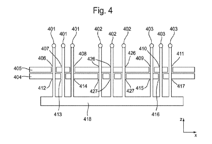
[0069] FIG. 4 is schematic diagram showing a cross-section through a stack of
two substrates
according to an embodiment.
CA 03172893 2022- 9- 22
WO 2021/190976 15
PCT/EP2021/056519
[0070] The substrate stack in FIG. 4 comprises a first substrate 404 and a
second substrate 405. The
first substrate 404 may be referred to as an up-beam substrate 404 because,
when the substrate stack is
illuminated by the light source 418, the first substrate is the first
substrate to be illuminated by
charged particles. The second substrate may be referred to as a down-beam
substrate. The first
substrate 404 comprises a first alignment opening set 412, 413, and 414. The
first substrate 404 also
comprises a second alignment opening set 415, 416, and 417. The first
substrate 404 also comprises a
beam path openings 427 for the charged particle beam paths of a multi-beam of
the charged particles.
The beam path openings 427 are arranged in a pattern in a major surface of the
first substrate 404
between the first alignment opening sets and the second alignment opening set.
[0071] The second substrate comprises a first alignment opening set 406, 407,
and 408. The second
substrate also comprises a second alignment opening set 409, 410, and 411. The
second substrate 405
also comprises a beam path openings 426 for the charged particle beam paths of
a multi-beam of the
charged particles. The beam path openings 426 are arranged in a pattern in a
major surface of the
second substrate 405 between the first alignment opening set and the second
alignment opening set.
[0072] The second substrate 405 may be an aperture array. When the substrate
stack is used in a
multi-beam charged particle apparatus, the aperture array is the major surface
the substrate stack that
is illuminated by charged particles. All of the beam path openings of the
second substrate 405 may
have a narrower diameter than the corresponding beam path openings of the
first substrate 404. The
beam path openings in the aperture array define sub-beams. The size and shape
of the sub-beams will
also be dependent on the beam manipulators along the beam path openings.
[0073] In the present embodiment, the second substrate 405 may be referred to
as a reference
substrate. The reference substrate is the substrate that the positions of the
other substrates in the
substrate stack arc defined relative to. Although any substrate in the
substrate stack may be used as a
reference substrate, the reference substrate is preferably the substrate that
comprises the aperture
array. This is because the substrate that comprises the aperture array defines
the sub-beams and may
therefore have a greater influence on the performance of the manipulator array
than any of the other
substrates in the substrate stack.
[0074] In FIG. 4, the diameter of each of the light spots 402 is dependent on
the diameter of the
beam part openings in the second substrate 405. The diameter of each of the
light spots 402 is not
dependent on the diameter of the beam part openings in the first substrate 404
because the beam path
openings in the first substrate 404 are have a larger diameter than those in
the second substrate.
[0075] In the first alignment opening set in the second substrate 405, the
alignment opening 407 has
a narrower diameter than the alignment openings 406 and 408. The alignment
opening 407 may be
located in between the other alignment openings 406 and 408. Similarly, in the
second alignment
opening set in the second substrate 405, the alignment opening 410 has a
narrower diameter than
alignment openings 409 and 411. The alignment opening 410 may be located in
between the other
alignment openings 409 and 411.
CA 03172893 2022- 9- 22
WO 2021/190976 16
PCT/EP2021/056519
[0076] In the first alignment opening set in the first substrate 404,
alignment openings 412 and 414
have a narrower diameter than alignment opening 413. The alignment opening 413
may be located in
between the other alignment openings 412 and 414. Similarly, in the second
alignment opening set in
the first substrate 404, alignment openings 415 and 417 have a narrower
diameter than opening 416.
The alignment opening 416 may be located in between the other alignment
openings 415 and 417.
[0077] The diameter of all of the alignment openings 412, 414, 415, 417, 407
and 410 may all be
substantially the same. Their diameter may be, for example, in the range 100
to 1500pm.
[0078] The diameter of all of the alignment openings 413, 416, 406, 408, 409
and 411 may all be
substantially the same. Their diameter may be, for example, ill the range 200
to 2000 um.
[0079] Light source 418 is configured to illuminate the alignment openings of
an exposed major
surface of the first substrate 404. When the exposed major surface of the
first substrate 404 is
illuminated, optical light beams 401 may pass through the first alignment
opening set in both the first
substrate 404 and the second substrate 405. Optical light beams 402 may also
pass through the beam
path openings in both the first substrate 404 and the second substrate 405.
Optical light beams 403
may also pass through the second alignment opening set in both the first
substrate 404 and the second
substrate 405.
[0080] For each light beam that has passed through an alignment opening, the
spot size of the light
beam may be only dependent on the smallest diameter of alignment opening that
the light beam has
passed through. Furthermore, the location of the light spot may be dependent
only on the location of
the substrate that comprises the alignment opening with the smallest diameter.
[0081] Accordingly, for the first substrate 404, alignment openings 412, 414,
415 and 417 may each
determine the spot size of the light beams that pass through these alignment
openings. This is because
the alignment openings 412, 414, 415 and 417 of the first substrate 404 all
have a narrower diameter
than the corresponding alignment openings 406, 408, 409 and 411 of the second
substrate 405. The
location of the light beams that pass through these alignment openings may
therefore be dependent on
the location of the first substrate 404 only and not the location of the
second substrate 405.
[0082] Similarly, for the second substrate 405, alignment openings 407 and 410
each determine the
spot size of the light beams that pass through these alignment openings. This
is because the alignment
openings 407 and 410 of the second substrate 405 both have a narrower diameter
than the
corresponding alignment openings 413 and 416 of the first substrate 404. The
location of the light
beams that pass through these alignment openings may therefore be dependent on
the location of the
second substrate 405 only and not the location of the first substrate 404.
[0083] The alignment openings 407 and 410 may be referred to as reference
openings because they
are located in the reference substrate and are openings that define the size
and location of a light spot.
The alignment openings 412, 414, 415 and 417 may be referred to as comparative
openings because
they arc not located in the reference substrate and arc openings that define
the size and location of a
light spot.
CA 03172893 2022- 9- 22
WO 2021/190976 17
PCT/EP2021/056519
[0084] Embodiments may determine the relative alignment of the substrates in
the substrate stack in
dependence on the relative positions of light beams that have passed through
the alignment openings.
In particular, the relative positions of the light spots generated in
dependence on the reference
openings 407 and 410, and the light spots generated in dependence on the
comparative openings 412,
414, 415, 417 may be used to determine the relative alignment of the first
substrate 404 and the
second substrate 405 (i.e. the reference substrate).
100851 The light beams may form light spots on a surface of a light detector,
such as a camera. The
light detector is not shown in FIG. 4. Each light spot may indicate the
position of a light beam that
has passed through the substrate stack. The light detector may generate a
signal corresponding to the
light spots formed. The light detector may comprise a processor that is
configured to generate data
indicative of the light spot locations from the generated signal. The light
detector may transmit the
signal to an external processor capable of generating said data indicative of
the light spot locations.
Embodiments include processing data indicative of the light spot locations so
as to compensate for
any tilt between the substrate stack and an optical axis of the light
detector. The data indicative of the
light spot locations may be provided to, and used by, an image generator to
generate one or more
images. The relative alignment of the substrates may be determined in
dependence on the relative
positions of the light spots in the one or more images. However, embodiments
also include
automatically using the data indicative of the light spot locations to
determine the alignment of the
substrates, without generating any images.
100861 All of the processes for determining the alignment of the substrates in
dependence on
obtained data indicative of the light spot locations may be performed by a
computing system. The
computing system may comprise an image generator.
100871 Embodiments include a tool for generating data indicative of the light
spot locations. The
tool may comprise a holder configured to hold a substrate stack. The tool may
comprise an
illuminator configured to illuminate at least part of one of the major
surfaces of the substrate stack.
The tool may comprise one or more light detectors for detecting the positions
of light beams. The
tool may comprise the above-described computing system for determining the
alignment of the
substrates in dependence on obtained data indicative of the light spot
locations. Alternatively, the
computing system may be remote from the tool.
[0088] In FIG. 4, each substrate has a substantially planar structure. The
plane of each substrate may
be defined as being in an x-y plane (in a Cartesian co-ordinate geometry). The
substrates are stacked
in a direction that is substantially orthogonal to the x-y plane, i.e. along a
z-axis in a z-direction. The
first substrate 404 is shown as being appropriately aligned with the second
substrate 405_ In
particular, the major surfaces of the substrates are in substantially parallel
planes and the beam path
openings in the substrates have corresponding locations.
[0089] The alignment opening sets in each substrate are configured so that the
reference openings
407 and 410, and the comparative openings 412, 414, 415, 417, are arranged
along a direction in the
CA 03172893 2022- 9- 22
WO 2021/190976 18
PCT/EP2021/056519
plane of the substrate stack, e.g. in the x-direction. The alignment openings
in the first alignment
opening set in the each substrate are arranged so that the reference opening
407 is located between the
two comparative openings 412 and 414. When the first and second substrates are
appropriately
aligned, a light spot corresponding to the reference opening 407 may be
equidistant to light spots
corresponding to the comparative openings 412 and 414. Similarly, the
alignment openings in the
first alignment opening set in the each substrate are arranged so that the
reference opening 410 is
located between the two comparative openings 415 and 417. When the first and
second substrates arc
appropriately aligned, a light spot corresponding to the reference opening 410
may be equidistant to
light spots corresponding to the comparative openings 415 and 417. in each
substrate, the beam path
openings may be aligned along an axis, such as the x-axis, with first and
second alignment opening
sets. The beam path openings may be equidistant to each of the first and
second alignment opening
sets.
[0090] In the planes of the substrates and along a direction orthogonal to the
x axis, i.e. along a y
axis, the alignment openings in each alignment opening set may have
substantially zero displacement.
100911 FIG. 5 shows a planar view of examples of four different relative
locations of light spots of
the light beams 401, 402 and 403 that have passed through alignment openings
in a substrate stack
comprising two substrates. The examples of four different relative locations
of light spots may
correspond to four different relative alignments of the first substrate 404
and the second substrate 405
shown in FIG. 4.
[0092] The first example 501 shows a light spot pattern when there is correct
alignment between the
first substrate 404 and the second substrate 405. The second to fourth
examples show light spot
patterns with three different types of misalignment.
100931 The relative locations of the light spots in the first example 501
indicate that the first and
second substrates are appropriately aligned in x, y and Rz (where Rz is the
amount of rotation about
the z-axis), as described above for FIG. 4. The light spots from both the
first alignment opening set
(which is the leftmost in FIG. 5) and the second alignment opening set (which
is the rightmost in
FIG. 5) are all substantially aligned along the x-axis. This indicates that
the substrates are
substantially aligned with respect to the y-direction and with the Rz
rotational position. That is there
is no substantial misalignment of the substrates in the y-direction and that
the Rz is appropriate. The
light spots from within both the first and second alignment opening sets are
all substantially equally
spaced in the x-direction. This indicates that the two substrates are
substantially aligned in the x-
direction. That is there is no substantial misalignment between the substrates
in the x-direction.
[0094] The relative locations of the generated light spots in the second
example 502 indicate that the
first and second substrates are appropriately aligned in y and Rz but are
misaligned in x. The light
spots from within both the first and second alignment opening sets are all
substantially lie on the x-
axis. This indicates that the substrates arc substantially aligned with
respect to the y-direction and
with the Rz rotational position. However, the detected light spots from within
both the first and
CA 03172893 2022- 9- 22
WO 2021/190976 19
PCT/EP2021/056519
second alignment opening sets are unequally spaced apart along the x-axis.
That is to say, the middle
light spot corresponding to each alignment opening set is displaced in the
same direction, and with the
same magnitude, from the central position between the light spots. This is
indicative of a
misalignment between the two substrates in the x-direction.
[0095] The relative locations of the generated light spots in the third
example 503 indicate that the
first and second substrates are appropriately aligned in x and Rz but are
misaligned in y. Some, but
not all, of the light spots from both the first and second alignment opening
sets lie on the x-axis. In
particular, the middle spots of each set have displacements in the y-
direction, relative to the other light
spots in each set, of similar displacement and direction. This indicates that
there is misalignment of
the substrates in the y-direction. Such a light spot pattern indicates of
rotational alignment in Rz. The
light spots from within both the first and second alignment opening sets are
all substantially equally
spaced along the x-direction and this indicates the substrates are aligned in
the x-direction. That is
there is no substantial misalignment of the two substrates in the x-direction.
[0096] The relative locations of the generated light spots in the fourth
example 504 indicate that the
first and second substrates arc appropriately aligned in x and y but arc
misaligned in Rz. The light
spots corresponding to the first alignment opening set are aligned in the x-
direction and the central
alignment opening is displaced by an amount in a y-direction which can be
referred to as a positive y-
direction. The light spots corresponding to the second alignment opening set
are aligned in the x-
direction and the central opening is displaced in the y-direction by the same
amount as the central spot
of the first alignment opening set but in the opposite y-direction, i.e. the
negative y-direction. This
similar magnitude of displacement in opposite directions of the central
alignment opening of both sets
indicates that the substrates are aligned in the y-direction and are
rotationally displaced in Rz, i.e.
around the z axis. That is, the two substrates arc misaligned in Rz. The light
spots from within both
the first and second sets of alignment openings are all substantially equally
spaced in the x-direction
and this indicates that the two substrates are substantially aligned in x-
direction; that is there is no
substantial misalignment of the substrates in the x-direction.
[0097] Accordingly, the relative locations of the light spots may be used to
determine the relative
locations of the first substrate 404 and the second substrate 405 in x, y, and
Rz. An actual substrate
misalignment in x, y and/or Rz may be determined to comprise a plurality of
separate misalignment
components, with each misalignment component being in one of x, y, and Rz. For
each substrate in
the substrate stack other than the reference substrate, tolerance levels may
be set for the relative
alignment components, in each of x, y, and Rz, of the substrate to the
reference substrate. The
tolerance levels may be referred to as degrees of freedom in the positioning
of each substrate. The
tolerance levels may be different for each substrate in the substrate stack. A
substrate stack may be
determined to be within an alignment performance specification if the relative
alignment components
of all of the substrates in the substrate stack to the reference substrate is
within the set tolerance levels.
CA 03172893 2022- 9- 22
WO 2021/190976 20
PCT/EP2021/056519
[0098] For each substrate in the substrate stack, there may be at least one
light beam path through the
substrate stack for which the spot size and location of the at least one light
beam may be dependent
only on the location of the said substrate. That is to say, for each substrate
in the substrate stack and
on at least one of the light beam paths, said substrate may comprise at least
one alignment opening
that has a narrower diameter than all of the corresponding alignment openings
of the other substrates
in the substrate stack.
100991 For different light beam paths, the narrowest diameter of alignment
opening that defines the
spot size may differ between different substrates. This allows the location of
each substrate in the
substrate stack to be individually identified by at least one light spot for
the substrate.
[00100] The number of alignment openings in each alignment opening set may be
dependent on the
number of substrates in the substrate stack. The number of alignment openings
in each alignment
opening set may be greater than, or equal to, the number of substrates in the
substrate stack such that,
for each substrate, there is at least one light spot that corresponds to only
its location. . In an
arrangement there is at least one more aperture than the number of substrates
in the substrate stack.
[00101] Embodiments may be used to determine the relative alignments of any
number of substrates
in the substrate stack. For example, the number of substrates in the substrate
stack may be 2 to 20.
[00102] Although embodiments include there being only one alignment opening
set, there are
preferably at least two alignment opening sets. Preferably, two alignment
opening sets are located at
opposite ends of a major surface of a substrate. For example, two alignment
opening sets may be
located at opposite ends of the x axis, as shown in Figure 5. A relatively
large spacing between the
sets of alignment openings increases the accuracy of the determination of the
Rz alignment.
[00103] As described above, the alignment opening sets may be provided on
either side of the beam
path openings. Each alignment opening set may bc spaced a substantial distance
from the beam path
openings such that the alignment openings do not affect, or otherwise
influence, the active areas of
each substrate, as may be required for providing beam manipulators
[00104] Embodiments may be used for determining if two or more substrates in a
substrate set that
have been bonded together are aligned in x, y, and Rz within the limits of a
performance specification.
If the alignment of the substrates is not within the performance
specification, a determination may be
made to scrap the set of substrates such that a final product comprising the
substrate sets is not
defective. Alternatively, a determination may be made to de-bond the
substrates and re-bond them
with adjusted alignments.
[00105] Embodiments may also be used for determining if a substrate stack,
that comprises two or
more substrate sets that have been bonded together, are appropriately aligned
in x, y, and Rz If the
substrate sets are not appropriately aligned, a determination may be made to
scrap the substrate stack
such that a final product comprising the substrate stack is not defective.
Alternatively, a
determination may be made to dc-bond the substrate sets and re-bond them with
adjusted alignments.
CA 03172893 2022- 9- 22
WO 2021/190976 21
PCT/EP2021/056519
[00106] For each substrate set that comprises a plurality of substrates, the
substrates may be arranged
such that for each substrate in the substrate set, there is at least one light
beam path through the
substrate set for which the spot size and location of the at least one light
beam is dependent only on
the location of the said substrate. Alternatively, the substrates may be
configured such that, for some
of the substrates, there are no light beam spot sizes and locations that are
dependent on the locations
of the substrates. This may be appropriate, for example, when the accuracy of
the x, y, and Rz
locations of some of the substrates in the set of substrates is not critical
for all of the substrates in the
set of substrates.
[00107] Embodiments also include determining the relative alignment in x, y
and Rz of substrates, or
substrate sets, before they have been bonded together. The light spot
locations may be used to adjust
the locations of the substrates, or substrate sets, in x, y and Rz so that the
substrates, or substrate sets,
are appropriately aligned prior to them being bonded together.
1001081 The configuration, i.e. arrangement, of alignment openings in each
alignment opening set
may be substantially the same. The alignment openings in each alignment
opening set may be
configured such that the alignment openings arc configured in a substantially
straight line.
Alternatively, the alignment openings in each alignment opening set may be
configured such that the
alignment openings are configured in a plurality of substantially straight
lines.
[00109] FIG. 6A shows a possible configuration of an alignment opening set.
The alignment
openings in each alignment opening set arc configured such that the alignment
openings arc
configured in two orthogonal substantially straight lines. The orthogonal
lines that alignments marks
are aligned along are parallel with x and y axes. It should be noted that FIG.
6A only shows
exemplary relative locations of the alignment openings. FIG. 6A does not
indicate the relative
diameters, i.e. sizes, of the alignment openings because these differ between
the substrates in the
substrate stack.
[00110] The alignment opening set shown in FIG. 6A may be used ill a substrate
stack that comprises
more than two substrates. For example, the alignment opening set may be used
for a substrate stack
that comprises five substrates. One of the substrates in the substrate stack
may be a reference
substrate that the alignments of the other substrates are determined relative
to. As described earlier,
the reference substrate may be a substrate for which the beam path openings
are an aperture array that
the sub-beam paths are defined by. The alignment opening 601 may be narrowest
in the reference
substrate. The alignment opening 601 may therefore be referred to as a
reference opening. For all of
the alignment openings 602, 603, 604, 605, 606 and 607 the narrowest alignment
openings is a
substrate other than the reference substrate. All of the alignment openings
602, 603, 604, 605, 606
and 607 may therefore be referred to as comparative openings.
[00111] The alignment openings 603 and 604 may both be narrowest in the same
substrate and
therefore comparative openings for said same substrate. An advantage of this
is that, when the
substrate comprising these comparative openings is correctly aligned with the
reference substrate, the
CA 03172893 2022- 9- 22
WO 2021/190976 22
PCT/EP2021/056519
light spots generated by the alignment openings 601, 603 and 604 are all
aligned in an x-direction and
equally spaced. The earlier described techniques with reference to FIG. 5 may
therefore be easily
used to determine any misalignment components.
[00112] Similarly, the alignment openings 606 and 607 may both be comparative
openings for the
same substrate, that is different from the substrate that has alignment
openings 603 and 604 as
alignment openings. When the substrate with alignment openings 606 and 607 as
comparative
openings is correctly aligned with the reference substrate, the light spots
generated by the alignment
openings 601, 606 and 607 are all aligned in a y-direction and equally spaced.
The earlier described
techniques with reference to FIG. 5 may therefore be easily used to determine
any misalignment
components.
[00113] The alignment opening 602 may be a comparative opening for a substrate
for which none of
the other alignment openings are a comparative opening. Only one light spot
will therefore be
indicative of the location of the substrate for which alignment opening 602 is
the comparative
opening. The displacements in the x and y directions of the light spots from
the comparative and
reference openings can be determined. From this, the relative alignments of
the substrate for which
alignment opening 602 is a comparative opening and the reference substrate may
be determined.
[00114] Similarly, the alignment opening 605 may be a comparative opening for
a substrate for which
none of the other alignment openings are a comparative opening. Only one light
spot will therefore
be indicative of the location of the substrate for which alignment opening 605
is the comparative
opening. The displacements in the x and y directions of the light spots from
the comparative and
reference openings can be determined. From this, the relative alignments of
the substrate for which
alignment opening 605 is a comparative opening and the reference substrate may
be determined.
[00115] The relative alignment to the reference substrate can be determined
with greater accuracy for
substrates with more than one comparative opening. However, whether or not the
alignment of a
substrate meets a performance specification may still be determined when there
is only one
comparative opening for a substrate. Accordingly, the substrates in the
substrate stack for with the
most critical alignment tolerances preferably have more than one comparative
opening. Having only
one comparative opening for the other substrates in the substrate stack may be
appropriate and
advantageously reduce the number of alignment openings that are required.
[00116] The alignment opening set shown in FIG. 6A may preferably be used
together with a further
alignment opening set. The further alignment opening set may be, for example,
the same as that
shown in FIG. 6A or as shown in FIG. 6B. The alignment opening set shown in
FIG. 6B may be a
substantial mirror image of the alignment opening set shown in FIG. 6A. That
is, the positions of the
alignment openings in the different alignment opening sets may have reflective
symmetry about a y-
axis. The alignment opening sets in FIGS. 6A and 6B may be provided at
opposite ends of the major
surface of a substrate. The alignment opening sets in FIG. 6B may be
configured so that the
alignment openings 601', 602', 603-, 604', 605', 606' and 607' provide the
same correspondence of
CA 03172893 2022- 9- 22
WO 2021/190976 23
PCT/EP2021/056519
reference and comparative openings to each substrate as the alignment openings
601, 602, 603, 604,
605, 606 and 607 in FIG. 6A.
[00117] The use of more than one alignment opening set increases the number of
comparative
openings that are provided. This both increases the accuracy with which any
misalignments may be
determined and the number of substrates for which one or more comparative
openings may be
provided.
[00118] Further alignment openings may be added to the two alignment opening
sets shown in FIGS.
6A and 6B. Each further alignment opening will provide a comparative opening
for a substrate in the
substrate stack. Preferably, each further alignment opening is either located
along the y-direction or
the x-direction so that it is displaced from the reference opening in only the
x-direction or only the y-
direction. However, an alignment opening may be positioned in an alignment
opening set at any
location so long as its relative position at least to the reference opening
407 can be determined. In
particular, embodiments include providing further alignment openings along a
diagonal relative to the
x and y directions in FIGS. 6A and 6B.
[00119] A substrate stack is typically provided on a printed circuit board,
PCB. The PCB may
provide both a physical support for the substrate stack and also electrical
connections to the substrates
in the substrate stack. The PCB may also support other components than the
substrate stack. The
manufacturing processes of a device may therefore comprise the process of
positioning the substrate
stack on a PCB. Embodiments include techniques for determining if a substrate
stack is appropriately
positioned on the PCB. The PCB is provided with PCB alignment structures that
can be used to
determine the relative alignment of the substrate stack and the PCB.
[00120] The PCB may be a planar structure with an upper major surface and a
lower major surface.
The substrate stack may be provided on the upper major surface of the PCB. The
dimensions of the
major surfaces of the PCB may be larger than the corresponding dimensions of
the major surfaces all
of the substrates in the substrate stack.
[00121] As described earlier, the substrate stack may comprise a plurality of
alignment opening sets
and also beam path openings. There may be a single large opening through the
PCB so that, in use,
the multi-beam of charged particles can travel through both the beam path
openings and the single
opening through the PCB. The single opening in the PCB may be large enough for
light beams to
both travel through the alignment opening sets and also through the PCB.
Alternatively, the PCB may
comprise further openings so that all of the light beams that pass through the
substrate stack can also
pass through the PCB.
[00122] As explained above, the PCB is provided with PCB alignment structures
that can he used to
determine the relative alignment of the substrate stack and the PCB. A PCB
alignment structure may
comprise a marker provided on the upper major surface of the PCB. The marker
may be, for example,
an optical reflector such as a fiducial mark. The marker may have a
characteristic pattern. A PCB
alignment structure may alternatively be a through passage through the PCB.
CA 03172893 2022- 9- 22
WO 2021/190976 24
PCT/EP2021/056519
1001231 Each PCB alignment structure may be spaced away from the area on the
upper major surface
of the PCB that is covered by the substrate stack after assembly. Each PCB
alignment structure is
therefore not covered by the substrate stack when the substrate stack is on
the PCB. The PCB
alignment structures may be arranged such that, when the substrate stack is
positioned on the PCB
with a correct alignment, the PCB alignment structures are, in plan view,
substantially linearly aligned
with the alignment opening sets in the stack. In an embodiment, the substrate
stack is arranged
between at least two PCB alignment structures and the PCB alignment structures
are substantially
linearly aligned with the alignment opening sets in the substrate stack in the
x direction.
[00124] Embodiments include determining the relative alignment of the PCB and
the substrate stack
by illuminating the upper major surfaces of the stack and the PCB. As
described earlier, illumination
by light beams, that are dependent on the position of the substrate stack, may
pass through both the
PCB and also the alignment opening sets and/or beam path openings through the
substrate stack. The
position of the susbtrate stack may be determined in dependence of the
position of light beams
through the alignment opening sets and/or the beam path openings.
[00125] The illumination will also generate reflected light beam(s) from each
PCB alignment structure
that is an optical reflector. The position of the PCB may be determined in
dependence on the position
of the reflected light beam(s).
1001261 The illumination will also generate transmitted light beam(s) that
pass through each PCB
alignment structure that is an opening through the PCB. The position of the
PCB may be determined
in dependence on the position of the transmitted light beam(s)
1001271 The relative alignment of the PCB and the substrate stack in x, y, and
Rz may be determined
in dependence on the relative positions of light spots from the light beams
that are dependent on the
position of the substrate stack and light spots from the light beams that are
dependent on the position
of the PCB.
[00128] The light spots from the transmitted light beam(s) may be generated
ill the same plane as light
spots from the light beams that have passed through the substrate stack. The
light spots from the
reflected light beam(s) may be generated in a different plane as light spots
from the other light beams.
1001291The light beams may form light spots on a surface of one or more light
detectors, such as a
cameras. Each light spot may indicate the position of a light beam that has
either passed through the
substrate stack or is dependent on the location of a PCB alignment structure.
A light spot signal may
be generated by each light detector on which a light spot is incident. Each
light spot signal may be
indicative of light spot location data generated by a photonic detector. Data
indicative of the light
spot locations may be generated and/or captured by the one or more light
detectors. Embodiments
include processing data indicative of the light spot locations so as to
compensate for any tilt between
PCB and/or substrate stack and the optical axes of the one or more light
detectors. The data indicative
of the light spot locations may be provided to, and used by, an image
generator to generate one or
more images and the relative alignment of the substrate stack and PCB may be
determined in
CA 03172893 2022- 9- 22
WO 2021/190976 25
PCT/EP2021/056519
dependence on the relative positions of the light spots in the one or more
images. However,
embodiments also include automatically using the data indicative of the light
spot locations to
determine the relative alignment of the substrate stack and PCB.
[00130] All of the processes for determining the alignment of the PCB and
substrate stack in
dependence on obtained data indicative of the light spot locations may be
performed by a computing
system. The computing system may comprise an image generator.
[00131] Embodiments include a tool for generating data indicative of the light
spot locations. Thc
tool may comprise a holder configured to hold a PCB with a substrate stack on
it. The tool may
comprise an illuminator configured to illuminate at least part of one of the
major surfaces of the PCB
and substrate stack. The tool may comprise one or more light detectors for
detecting the positions of
light beams. The tool may comprise the above-described computing system for
determining the
alignment of the PCB and substrate stack in dependence on obtained data
indicative of the light spot
locations. Alternatively, the computing system may be remote from the tool.
[00132] Embodiments may be used for determining if a PCB and substrate stack
that have been
bonded together arc aligned in x, y, and Rz within the limits of a performance
specification. If the
alignment is not within the performance specification, a determination may be
made to scrap the PCB
and substrate stack such that a final product comprising the substrate stack
on the PCB is not
defective. Alternatively, a determination may be made to de-bond the substrate
stack and PCB. The
substrate stack and PCB may then be re-bonded with corrected alignments.
[00133] Embodiments also include a technique for determining the relative Rx,
Ry and z positions of
substrates in a substrate stack.
[00134] As described earlier, each substrate in the substrate stack has a
substantially planar structure
that is substantially in the x-y plane. The substrates in the substrate stack
arc stacked in the z-
direction. The rotational displacement about the x-direction is referred to as
Rx. The rotational
displacement about the y-direction is referred to as Ry. The upper major
surface of each substrate in
the substrate stack may be substantially planar, for example rectangular. The
sides of the rectangle
may be substantially in the x-direction and the y-direction, respectively.
[00135] For each substrate in the substrate stack, its dimensions in the x-
direction and the y-direction
may be greater than or equal to that of all of the substrates in the substrate
stack that are above it.
That is to say, the uppermost substrate in the substrate stack may have the
smallest dimensions in the
x-direction and the y-direction of all of the substrates in the substrate
stack. The dimensions in the x-
direction and the y-direction of each other substrate in the substrate stack
may be greater than or equal
to that of the substrate immediately above it. The substrate stack may have
the appearance of a step
pyramid, with each step corresponding to an exposed portion of a major surface
of a substrate in the
substrate stack. The substrate stack may be of stepped substrates of
successively smaller cross-
sectional area.
CA 03172893 2022- 9- 22
WO 2021/190976 26
PCT/EP2021/056519
[00136] Embodiments include using an optical height sensor to generate a
height map over the upper
surface of the substrate stack. A number of known optical height sensors may
be used. These may
measure the distance in the z-direction to a surface in dependence on emitted
and reflected light.
beams. The light beams may be as laser beams. The height map shows the z-
position of the exposed
surfaces of the upper major surfaces of each of the substrates in the
substrate stack. Embodiments
include using the variation in the z-positions provided by the optical height
map to determine the
relative Rx, Ry and z positions of the substrates in the substrate stack.
[00137] Embodiments also include obtaining an optical height map of a
substrate stack on the PCB
and using the optical height map to determine the relative Rx, Ry and z
positions of the PCB and the
substrate stack.
[00138] Embodiments include a number of modifications and variations to the
techniques described
above.
1001391In FIG. 4, light spots are generated by illuminating a substrate stack
with light from a light
source 418 that is positioned below the substrate stack. Embodiments also
include generating light
spots by illuminating a substrate stack with light from a light source 418
that is positioned above the
substrate stack.
[00140] The multi-beam charged particle apparatus could be a component of an
inspection (or metro-
inspection) tool or part of an e-beam lithography tool. The multi-beam charged
particle apparatus
according to embodiments may be used in a number of different applications
that include electron
microscopy in general, not just SEM, and lithography.
1001411Embodiments include a multi-beam inspection and/or metrology tool that
comprises a beam
manipulator device that has been made according to the techniques of
embodiments. The beam
manipulator device may be part of a scanning device arranged to project a
multi-beam of charged
particles onto a sample. The multi-beam inspection tool may comprise a
detector that is arranged to
detect charged particles, such as secondary electrons, that are received from
the illuminated sample_
[00142] Embodiments also include a multi-beam lithography tool that comprises
the above-described
beam manipulator device.
[00143] In particular, the multi-beam charged particle apparatus may comprise
both the above
described beam manipulator device and any of the components of the apparatuses
described above
with reference to FIGS. 1 to 3.
1001441 The multi-beam charged particle apparatus may comprise a single source
of charged particles,
as shown in FIGS. 1 to 3. Alternatively, the multi-beam charged particle
apparatus may comprise a
plurality of sources of charged particles. There may be a separate column for
each source and a
manipulator devices according to embodiments provided in each column.
Alternatively, the multi-
beam charged particle apparatus may comprise a plurality of sources of charged
particles and only a
single column.
CA 03172893 2022- 9- 22
WO 2021/190976 27
PCT/EP2021/056519
[00145] Throughout embodiments a z-direction is described and this may be the
charged particle
optical axis. This axis describes the path of charged particles through, and
output from, the
illumination apparatus. The sub-beams of an output multi-beam may all be
substantially parallel to
the charged particle optical axis. The charged particle optical axis may be
the same as, or different
from, a mechanical axis of the illumination apparatus.
[00146] A particularly preferred application of embodiments is in the
manufacture and testing of a
substrate stack and PCB for use as a beam manipulator in a charged particle
apparatus. However, the
techniques of embodiments may more generally be applied in the manufacture and
testing of any
substrate stack and PCB for use any application. Embodiments allow the
alignment of the substrates
in the substrate stack to be determined. Embodiments may also be used to
determine the relative
alignment of a PCB and any component positioned on the PCB.
[00147] Embodiments include the following statements.
1001481 According to a first aspect of the invention, there is provided a
substrate stack comprising a
plurality of substrates, wherein: each substrate in the substrate stack
comprises at least one alignment
opening set; the at least one alignment opening set in each substrate is
aligned for a light beam to pass
through corresponding alignment openings in each substrate; and each substrate
comprises at least one
alignment opening that has a smaller diameter than the corresponding alignment
openings in the other
substrates.
[00149] Preferably, each substrate in the substrate stack comprises a
plurality of alignment opening
sets; and each alignment opening set of each substrate in the substrate stack
is configured such that,
for each one of the substrates in the substrate stack, there is at least one
light beam path through the
alignment opening sets that is indicative of the position of said one
substrate relative to the other
substrates.
[00150] Preferably, the alignment openings in each alignment opening set are
configured such that the
alignment openings make a pattern that includes a substantially straight line_
[00151] Preferably, the alignment openings in each alignment opening set are
configured such that the
alignment openings make a pattern that includes a plurality of substantially
straight lines.
[00152] Preferably, the alignment openings in each alignment opening set are
configured such that the
alignment openings make a pattern that includes two substantially straight
lines that intersect each
other substantially orthogonally.
1001531 Preferably, the substrate stack comprises an array of beam
manipulators; and each beam
manipulator in the array is configured to manipulate a sub-beam of a multi-
beam of charged particles.
[00154] Preferably, the array of beam manipulators is an N by M array; N is
between 2 and 20, such
as 5; and M is between 2 and 20, such as 5.
[00155] Preferably: each substrate comprises at least first and second
alignment opening sets; each
alignment opening set on a substrate is on a different part of the substrate
to the array of beam
CA 03172893 2022- 9- 22
WO 2021/190976 28
PCT/EP2021/056519
manipulators; and the array of beam manipulators is arranged between the first
alignment opening set
and the second alignment opening set.
[00156] Preferably, the first and second alignment opening sets of each
substrate are located at
opposite ends of a major surface of the substrate.
[00157] According to a second aspect of the invention, there is provided a
method for determining the
alignment of substrates in a substrate stack that comprises a plurality of
substrates, the method
comprising: determining the positions of a plurality of light beams that have
passed through a
respective plurality of alignment openings defined in each substrate in the
substrate stack; and
determining the relative x, y, and Rz alignments of at least two substrates in
the substrate stack in
dependence on the determined positions; wherein: for each light beam path
through the substrate
stack, the alignment opening of one of the substrates on the light beam path
has a smaller diameter
than all of one or more other alignment openings of respective one or more
other substrates on the
light beam path; and for each one of at least two of the plurality of light
beam paths, a different one of
the substrates on the light beam path has an alignment opening with a smaller
diameter than all of one
or more other alignment openings of respective one or more other substrates on
the light beam path
such that, for each one of at least two substrates in the substrate stack,
there are one or more light
beams paths with positions that are indicative of the position of only said
one substrate.
[00158] Preferably, the alignment opening diameters in all of the substrates
are configured such that,
for each one of the substrates, the positions of one or more light beam paths
arc dependent on only
said one substrate.
1001591 Preferably, each substrate in the substrate stack has a substantially
planar structure; and the
substrates in the substrate stack are stacked in a direction that
substantially orthogonal to the planar
structure.
[00160] Preferably, each substrate in the substrate stack comprises a
plurality of alignment opening
sets; and each alignment opening set of each substrate in the substrate stack
is configured such that,
for each one of the substrates in the substrate stack, there is at least one
light beam path through the
alignment opening sets that is indicative of the position of said one
substrate relative to the other
substrates.
1001611 Preferably, the configuration of alignment openings in each alignment
opening set is
substantially the same.
1001621 Preferably, the alignment openings in each alignment opening set are
configured such that the
alignment openings make a pattern that includes a substantially straight line.
[00163] Preferably, the alignment openings in each alignment opening set are
configured such that the
alignment openings make a pattern that includes a plurality of substantially
straight lines.
[00164] Preferably, the alignment openings in each alignment opening set are
configured such that the
alignment openings make a pattern that includes two substantially straight
lines that intersect each
other substantially orthogonally.
CA 03172893 2022- 9- 22
WO 2021/190976 29
PCT/EP2021/056519
[00165] Preferably, the substrate stack comprises an array of beam
manipulators; and each beam
manipulator in the array is configured to manipulate a sub-beam of a multi-
beam of charged particles.
[00166] Preferably, one or more of the substrates comprises at least part of
one or more beam
manipulators in the array of beam manipulators.
[00167] Preferably, the array of beam manipulators is an N by M array; N is
between 2 and 20, such
as 5; and M is between 2 and 20, such as 5.
1001681 Preferably: each substrate comprises at least first and second
alignment opening sets; each
alignment opening set on a substrate is on a different part of the substrate
to the array of beam
manipulators; and the array of beam manipulators is arranged between the first
alignment opening set
and the second alignment opening set.
[00169] Preferably, the first and second alignment openings of each substrate
are located at opposite
ends of a major surface of the substrate.
1001701 Preferably, the arrangement of the alignment openings in the first
alignment opening set has
mirror symmetry with the arrangement of the alignment openings in the second
alignment opening
set.
[00171] Preferably, the method further comprises: illuminating the alignment
openings on the
substrate stack of substrates such that a plurality of light beams travel
through the substrate stack;
obtaining data indicative of the light beam locations; determining the
relative alignment of substrates
in the substrate stack in dependence on the data indicative of the light beam
locations.
[00172] Preferably, the method further comprises generating one or more images
that indicate the
relative positions of the plurality of light beams in dependence on the data
indicative of the light beam
locations.
1001731 Preferably, the data indicative of the light beam locations is
obtained by a light detector, and
the method further comprises processing the data indicative of the light beam
locations so as to
compensate for any tilt between the substrate stack and an optical axis of the
light detector.
[00174] Preferably the method further comprises determining if the alignment
of substrates within the
substrate stack meets a performance specification in dependence on the
determined x, y, and Rz
alignment of the substrates.
1001751 According to a third aspect of the invention, there is provided a
computing system configured
to determine the alignment of substrates in a substrate stack by performing
the method according to
the second aspect.
[00176] According to a fourth aspect of the invention, there is provided a
tool for obtaining data
indicative of light beam locations, the tool comprising: a stack holder
configured to hold a substrate
stack according to the first aspect; an illuminator configured to illuminate
at least part of a surface of
the substrate stack; and a light detector configured to generate data
indicative of the light beam
locations in dependence on a plurality of light beams that have passed through
the substrate stack.
CA 03172893 2022- 9- 22
30
[00177]According to a fifth aspect of the invention, there is provided a
system comprising the tool
according to the fourth aspect and the computing system according to the third
aspect.
[00178]According to a sixth aspect of the invention, there is provided a
method for determining the
alignment of substrates in a substrate stack, the substrate stack having at
least two substrates, wherein
in each of the substrates there are a plurality of alignment openings that
align with corresponding
alignment openings in the other substrates of the substrate stack such that
there is a through passage
through the substrate stack associated with each alignment opening in each
substrate, the method
comprising: determining the relative positions of a plurality of light beams,
each light beam having
passed along a light path through the substrate stack via a respective through
passage; and
determining the relative x, y, and Rz alignments of the substrates in the
substrate stack in dependence
on the determined positions; wherein: the alignment opening of one of the
substrates that defines the
through passage for a corresponding light path through the through passage has
a smaller diameter
than the other alignment openings that define the through passage; and for
each light path a different
substrate in the substrate stack has an diameter with a smaller diameter than
the other alignment
openings that define the corresponding through passage in the substrate stack.
[00179] Preferably, the light paths are configured such that: each light path
has a position indicative of
one substrate in the substrate stack relative to the other substrate in the
substrate stack, and/or the
relative positions of the light paths are indicative of the x, y, and Rz
alignments of the substrates in the
substrate stack.
[00180] According to a seventh aspect of the invention, there is provided a
substrate stack of
substrates comprising beam manipulators, the substrate stack having at least
two substrates, wherein
in each substrate there are a plurality of alignment openings that align with
corresponding alignment
openings in the other substrates of the substrate stack such that there is a
through passage through the
substrate stack associated with each alignment opening in each substrate,
wherein each of the plurality
of through passages is for the passage of a light beam and the light beams are
suitable for determining
the relative x, y, and Rz alignments of the substrates in the substrate stack;
wherein: the alignment
opening of one of the substrates, that defines the through passage fora
corresponding light path
through the through passage, has a smaller diameter than the other alignment
openings that define the
through passage; and a different substrate in the substrate stack has an
alignment opening with a
smaller diameter than the other alignment openings that define the
corresponding through passage in
the substrate stack.
[00181] Preferably, each through passage is for passage of a different light
path; each light path has a
position indicative of one substrate in the substrate stack relative to the
other substrates in the
substrate stack; and/or the relative positions of the light paths are
indicative of the x, y, and Rz
alignments of the substrates in the substrate stack.
[00182]According to an eighth aspect of the invention, there is provided a
combination of a printed
circuit board, PCB, and the substrate stack as described herein, the substrate
stack being provided on
CA 03172893 2022- 9- 22
31
the PCB, wherein: in the PCB is defined an opening configured to be aligned
with the through
passage in the substrate stack for interacting with a stack light source; and
a surface of the PCB
comprises a plurality of alignment structures configured to interact with a
PCB light source.
[00183] Preferably, the PCB and the substrate stack are configured so that
interaction of the stack light
source with the through passage in the substrate stack and the corresponding
opening in the PCB and
the interaction of the PCB light source with the plurality of alignment
structures enables the relative x,
y, and Rz alignments of the substrate stack and the PCB to be determined.
[00184]According to a ninth aspect of the invention, there is provided a
combination of a printed
circuit board, PCB, and substrate stack in which is defined a plurality of
through passages for beam
path openings, the substrate stack being provided on the PCB, wherein in a
surface of the PCB is a
plurality of alignment structures configured to interact with a light source
for enabling the alignment
of the PCB to be determined.
[00185]According to a tenth aspect of the invention, there is provided a
method for determining the
relative alignments of a substrate stack and a printed circuit board, PCB,
wherein the substrate stack is
provided on the PCB, the method comprising: determining the positions of a
first plurality of light
beams that have passed through both a respective plurality of openings through
the substrate stack and
at least one opening in the PCB; determining the positions of a second
plurality of light beams that are
dependent on a plurality of PCB alignment structures; and determining the
relative x, y, and Rz
alignments of the substrate stack and the PCB in dependence on the determined
positions of the first
and second plurality of light beams.
[00186] Preferably, the PCB alignment structures comprise markers on the PCB
that are configured to
reflect at least some of the second plurality of light beams; wherein the
positions of the second
plurality of light beams are determined after the second plurality of light
beams have been reflected
off a respective plurality of markers on the PCB.
[00187] Preferably, the PCB alignment structures comprise one or more
alignment openings in the
PCB; wherein the positions of the second plurality of light beams are
determined after the second
plurality of light beams has passed through a respective plurality of
alignment openings through the
PCB.
[00188] Preferably, none of the second plurality of light beams passes through
the substrate stack.
[00189] Preferably, the method further comprises: illuminating the PCB and the
substrate stack;
obtaining data that indicates the positions of the first and second plurality
of light beams; and
determining the relative x, y, and Rz alignments of the substrate stack and
the PCB in dependence on
the obtained data that indicates the positions of the first and second
plurality of light beams.
[00190] Preferably, the one more images are generated by a light detector, and
the method further
comprises processing data that indicates the positions of the first and second
plurality of light beams
so as to compensate for any tilt between the substrate stack and an optical
axis of the light detector.
CA 03172893 2022- 9- 22
WO 2021/190976 32
PCT/EP2021/056519
[00191] Preferably, the method further comprises determining if the relative
alignment of the PCB and
substrate stack meets a performance specification in dependence on the
determined x, y, and Rz
alignments.
[00192] According to a eleventh aspect of the invention, there is provided a
computing system
configured to determine the alignment of a PCB and a substrate stack by
performing the method
according to the tenth aspect.
[00193] While the present invention has been described in connection with
various embodiments,
other embodiments of the invention will be apparent to those skilled in the
art from consideration of
the specification and practice of the invention disclosed herein. It is
intended that the specification and
examples be considered as exemplary only, with a true scope and spirit of the
invention being
indicated by the following claims and clauses.
[00194] There is provided the following clauses; Clause 1: A substrate stack
comprising a plurality of
substrates, wherein: each substrate in the substrate stack comprises at least
one alignment opening set;
the at least one alignment opening set in each substrate is aligned for a
light beam to pass through
corresponding alignment openings in each substrate; and each substrate
comprises at least one
alignment opening that has a smaller diameter than the corresponding alignment
openings in the other
substrates.
[00195] Clause 2: The substrate stack according to clause 1, wherein each
substrate in the substrate
stack comprises a plurality of alignment opening sets; and each alignment
opening set of each
substrate in the substrate stack is configured such that, for each one of the
substrates in the substrate
stack, there is at least one light beam path through the alignment opening
sets that is indicative of the
position of said one substrate relative to the other substrates.
[00196] Clause 3: The substrate stack according to any of clauses 1 or 2,
wherein the alignment
openings in each alignment opening set are configured such that the alignment
openings make a
pattern that includes a substantially straight line
[00197] Clause 4: The substrate stack according to any of clauses 1 or 2,
wherein the alignment
openings in each alignment opening set are configured such that the alignment
openings make a
pattern that includes a plurality of substantially straight lines.
1001981 Clause 5: The substrate stack according to clause 1 or 2, wherein the
alignment openings in
each alignment opening set are configured such that the alignment openings
make a pattern that
includes two substantially straight lines that intersect each other
substantially orthogonally.
[00199] Clause 6: The substrate stack according to any preceding clause,
wherein the substrate stack
comprises an array of beam manipulators; and each beam manipulator in the
array is configured to
manipulate a sub-beam of a multi-beam of charged particles.
[00200] Clause 7: The substrate stack according to clause 6, wherein the array
of beam manipulators
is an N by M array; N is between 2 and 20, such as 5; and M is between 2 and
20, such as 5.
CA 03172893 2022- 9- 22
WO 2021/190976 33
PCT/EP2021/056519
[00201] Clause 8: The substrate stack according to any preceding clause,
wherein: each substrate
comprises at least first and second alignment opening sets; each alignment
opening set on a substrate
is on a different part of the substrate to the array of beam manipulators; and
the array of beam
manipulators is arranged between the first alignment opening set and the
second alignment opening
set.
[00202] Clause 9: The substrate stack according to clause 8, wherein the first
and second alignment
opening sets of each substrate arc located at opposite ends of a major surface
of the substrate.
[00203] Clause 10: A method for determining the alignment of substrates in a
substrate stack that
comprises a plurality of substrates, the method comprising: determining the
positions of a plurality of
light beams that have passed through a respective plurality of alignment
openings defined in each
substrate in the substrate stack; and determining the relative x, y, and Rz
alignments of at least two
substrates in the substrate stack in dependence on the determined positions;
wherein: for each light
beam path through the substrate stack, the alignment opening of one of the
substrates on the light
beam path has a smaller diameter than all of one or more other alignment
openings of respective one
or more other substrates on the light beam path; and for each one of at least
two of the plurality of
light beam paths, a different one of the substrates on the light beam path has
an alignment opening
with a smaller diameter than all of one or more other alignment openings of
respective one or more
other substrates on the light beam path such that, for each one of at least
two substrates in the
substrate stack, there are one or more light beams paths with positions that
are indicative of the
position of only said one substrate.
1002041 Clause 11: The method according to clause 10, wherein the alignment
opening diameters in all
of the substrates are configured such that, for each one of the substrates,
the positions of one or more
light beam paths arc dependent on only said one substrate.
[00205] Clause 12: The method according to clause 10 or 11, wherein each
substrate in the substrate
stack has a substantially planar structure; and the substrates in the
substrate stack are stacked in a
direction that substantially orthogonal to the planar structure.
[00206] Clause 13: The method according to any of clauses 10 to 12, wherein
each substrate in the
substrate stack comprises a plurality of alignment opening sets; and each
alignment opening set of
each substrate in the substrate stack is configured such that, for each one of
the substrates in the
substrate stack, there is at least one light beam path through the alignment
opening sets that is
indicative of the position of said one substrate relative to the other
substrates.
[00207] Clause 14: The method according to any of clause 13, wherein the
configuration of alignment
openings in each alignment opening set is substantially the same.
[00208] Clause 15: The method according to any of clauses 13 or 14, wherein
the alignment openings
in each alignment opening set are configured such that the alignment openings
make a pattern that
includes a substantially straight line.
CA 03172893 2022- 9- 22
WO 2021/190976 34
PCT/EP2021/056519
[00209] Clause 16: The method according to any of clauses 13 or 14, wherein
the alignment openings
in each alignment opening set are configured such that the alignment openings
make a pattern that
includes a plurality of substantially straight lines.
1002101 Clause 17: The method according to any of clauses 13 or 14, wherein
the alignment openings
in each alignment opening set are configured such that the alignment openings
make a pattern that
includes two substantially straight lines that intersect each other
substantially orthogonally.
[00211] Clause 18: The method according to any of clauses 10 to 17, wherein
the substrate stack
comprises an array of beam manipulators; and each beam manipulator in the
array is configured to
manipulate a sub-beam of a multi-beam of charged particles.
[00212] Clause 19: The method according to clause 18, wherein one or more of
the substrates
comprises at least part of one or more beam manipulators in the array of beam
manipulators.
[00213] Clause 20: The method according to clause 18 or 19, wherein the array
of beam manipulators
is an N by M array; N is between 2 and 20, such as 5; and M is between 2 and
20, such as 5.
[00214] Clause 21: The method according to any of clauses 13 to 20, wherein:
each substrate
comprises at least first and second alignment opening sets; each alignment
opening set on a substrate
is on a different part of the substrate to the array of beam manipulators; and
the array of beam
manipulators is arranged between the first alignment opening set and the
second alignment opening
set.
[00215] Clause 22: The method according to clause 21, wherein the first and
second alignment
openings of each substrate are located at opposite ends of a major surface of
the substrate.
1002161 Clause 23: The method of clause 21 or 22, wherein the arrangement of
the alignment
openings in the first alignment opening set has mirror symmetry with the
arrangement of the
alignment openings in the second alignment opening set.
[00217] Clause 24: The method according to any of clauses 10 to 23, further
comprising: illuminating
the alignment openings on the substrate stack of substrates such that a
plurality of light beams travel
through the substrate stack; obtaining data indicative of the light beam
locations; determining the
relative alignment of substrates in the substrate stack in dependence on the
data indicative of the light
beam locations.
1002181 Clause 25: The method according to clause 24, further comprising
generating one or more
images that indicate the relative positions of the plurality of light beams in
dependence on the data
indicative of the light beam locations.
[00219] Clause 26: The method according to clause 24 or 25, wherein the data
indicative of the light
beam locations is obtained by a light detector, and the method further
comprises processing the data
indicative of the light beam locations so as to compensate for any tilt
between the substrate stack and
an optical axis of the light detector.
CA 03172893 2022- 9- 22
WO 2021/190976 35
PCT/EP2021/056519
[00220] Clause 27: The method according to any of clauses 10 to 26, further
comprising determining
if the alignment of substrates within the substrate stack meets a performance
specification in
dependence on the determined x, y, and Rz alignment of the substrates.
[00221] Clause 28: A computing system configured to determine the alignment of
substrates in a
substrate stack by performing the method according to any of clauses 10 to 27.
[00222] Clause 29: A tool for obtaining data indicative of light beam
locations, the tool comprising:
a stack holder configured to hold a substrate stack according to any of
clauses 1 to 9; an illuminator
configured to illuminate at least part of a surface of the substrate stack;
and a light detector
configured to generate data indicative of the light beam locations in
dependence on a plurality of light
beams that have passed through the substrate stack.
[00223] Clause 30: A system comprising the tool according to clause 29 and the
computing system
according to clause 28.
1002241 Clause 31: A method for determining the alignment of substrates in a
substrate stack, the
substrate stack having at least two substrates, wherein in each of the
substrates there are a plurality of
alignment openings that align with corresponding alignment openings in the
other substrates of the
substrate stack such that there is a through passage through the substrate
stack associated with each
alignment opening in each substrate, the method comprising: determining the
relative positions of a
plurality of light beams, each light beam having passed along a light path
through the substrate stack
via a respective through passage; and determining the relative x, y, and Rz
alignments of the
substrates in the substrate stack in dependence on the determined positions;
wherein: the alignment
opening of one of the substrates that defines the through passage for a
corresponding light path
through the through passage has a smaller diameter than the other alignment
openings that define the
through passage; and for each light path a different substrate in the
substrate stack has an diameter
with a smaller diameter than the other alignment openings that define the
corresponding through
passage in the substrate stack.
[00225] Clause 32: The method according to clause 31, wherein the light paths
are configured such
that: each light path has a position indicative of one substrate in the
substrate stack relative to the
other substrate in the substrate stack, and/or the relative positions of the
light paths are indicative of
the x, y, and Rz alignments of the substrates in the substrate stack.
[00226] Clause 33: A substrate stack of substrates comprising beam
manipulators, the substrate stack
having at least two substrates, wherein in each substrate there are a
plurality of alignment openings
that align with corresponding alignment openings in the other substrates of
the substrate stack such
that there is a through passage through the substrate stack associated with
each alignment opening in
each substrate, wherein each of the plurality of through passages is for the
passage of a light beam and
the light beams are suitable for determining the relative x, y, and Rz
alignments of the substrates in
the substrate stack; wherein: the alignment opening of one of the substrates,
that defines the through
passage for a corresponding light path through the through passage, has a
smaller diameter than the
CA 03172893 2022- 9- 22
WO 2021/190976 36
PCT/EP2021/056519
other alignment openings that define the through passage; and a different
substrate in the substrate
stack has an alignment opening with a smaller diameter than the other
alignment openings that define
the corresponding through passage in the substrate stack.
[00227] Clause 34: The substrate stack of substrates according to clause 33,
each through passage is
for passage of a different light path; each light path has a position
indicative of one substrate in the
substrate stack relative to the other substrates in the substrate stack;
and/or the relative positions of
the light paths arc indicative of the x, y, and Rz alignments of the
substrates in the substrate stack.
[00228] Clause 35: A combination of a printed circuit board, PCB, and the
substrate stack of clause 33
or 34, the substrate stack being provided on the PCB, wherein in the PCB is
defined an opening
configured to be aligned with the through passage in the substrate stack for
interacting with a stack
light source; an a surface of the PCB comprises a plurality of alignment
structures configured to
interact with a PCB light source.
1002291 Clause 36: The combination of clause 35, wherein the PCB and the
substrate stack are
configured so that interaction of the stack light source with the through
passage in the substrate stack
and the corresponding opening in the PCB and the interaction of the PCB light
source with the
plurality of alignment structures enables the relative x, y, and Rz alignments
of the substrate stack and
the PCB to be determined.
[00230] Clause 37: A combination of a printed circuit board, PCB, and
substrate stack in which is
defined a plurality of through passages for beam path openings, the substrate
stack being provided on
the PCB, wherein in a surface of the PCB is a plurality of alignment
structures configured to interact
with a light source for enabling the alignment of the PCB to be determined.
[00231] Clause 38: A method for determining the relative alignments of a
substrate stack and a printed
circuit board, PCB, wherein the substrate stack is provided on the PCB, the
method comprising:
determining the positions of a first plurality of light beams that have passed
through both a respective
plurality of openings through the substrate stack and at least one opening in
the PCB; determining the
positions of a second plurality of light beams that are dependent on a
plurality of PCB alignment
structures; and determining the relative x, y, and Rz alignments of the
substrate stack and the PCB in
dependence on the determined positions of the first and second plurality of
light beams.
1002321 Clause 39: The method according to clause 38, wherein the PCB
alignment structures
comprise markers on the PCB that are configured to reflect at least some of
the second plurality of
light beams; wherein the positions of the second plurality of light beams are
determined after the
second plurality of light beams have been reflected off a respective plurality
of markers on the PCB.
[00233] Clause 40: The method according to clause 39, wherein the PCB
alignment structures
comprise one or more alignment openings in the PCB; wherein the positions of
the second plurality
of light beams are determined after the second plurality of light beams has
passed through a respective
plurality of alignment openings through the PCB.
CA 03172893 2022- 9- 22
WO 2021/190976 37
PCT/EP2021/056519
[00234] Clause 41: The method according to any of clauses 38 to 40, wherein
none of the second
plurality of light beams passes through the substrate stack.
[00235] Clause 42: The method according to any of clauses 38 to 41, further
comprising: illuminating
the PCB and the substrate stack; obtaining data that indicates the positions
of the first and second
plurality of light beams; and determining the relative x, y, and Rz alignments
of the substrate stack
and the PCB in dependence on the obtained data that indicates the positions of
the first and second
plurality of light beams.
[00236] Clause 43: The method according to any of clauses 38 to 41, wherein
the one more images
are generated by a light detector, and the method further comprises processing
data that indicates the
positions of the first and second plurality of light beams so as to compensate
for any tilt between the
substrate stack and an optical axis of the light detector.
1002371 Clause 44: The method according to any of clauses 38 to 41, further
comprising determining
if the relative alignment of the PCB and substrate stack meets a performance
specification in
dependence on the determined x, y, and Rz alignments.
[00238] Clause 45: A computing system configured to determine the alignment of
a PCB and a
substrate stack by performing the method according to any of clauses 38 to 44.
1002391 The descriptions above are intended to be illustrative, not limiting.
Thus, it will be apparent
to one skilled in the art that modifications may be made as described without
departing from the scope
of the claims set out below and clauses provided above.
CA 03172893 2022- 9- 22