Note: Descriptions are shown in the official language in which they were submitted.
WO 2021/194931
PCT/US2021/023412
PRINT HEADS AND CONTINUOUS PROCESSES FOR PRODUCING ELECTRICALLY
CONDUCTIVE MATERIALS
CROSS REFERENCE TO RELATED APPLICATIONS
[0001] This application claims the benefit of U.S. provisional
application numbers
62/994,533 and 62/994,553, both filed March 25, 2020, the entirety of each of
which are
incorporated by reference herein.
TECHNICAL FIELD
[0002] This application is generally directed to the field of
electrically conductive
materials, such as textiles, yarns, fibers and fabrics, and more particularly
to continuous processes
for producing electrically conductive textiles, such as yarn, fiber or fabric.
BACKGROUND
[0003] Conventional processes for producing materials, such as
textiles, fibers, yarns, and
fabrics are solvent based. In those processes, raw materials or partially
finished fibers and yarns
can be colored with dyes, and treated for color fastness, feel, etc. In
conventional processes, the
items to be processed are introduced into vats containing treatment chemicals,
surfactants and
lubricants in a solvent. After processing, excess chemicals in the fabric are
rinsed out using more
solvent, leading to contaminated rivers and groundwater. The environmental
impacts of such
processes are significant, but these conventional techniques are widely used
because they offer
high-throughput production of conventional fibers and fabrics.
[0004] In addition to the environmental impact of conventional
processes, these processes
are not capable of producing electrically conductive yarn, fibers or fabric
that are mechanically
robust and can withstand multiple washings. The unsuitability arises due to
incompatibilities
between the chemistry, substrate and form/function of electrically conductive
fabrics and
conventional processes.
[0005] Therefore, a prevailing need in the field exists for
improved processes for producing
yarns, fibers and fabrics, including those that are compatible with
electrically conductive materials.
1
CA 03173022 2022- 9- 22
WO 2021/194931
PCT/US2021/023412
BRIEF DESCRIPTION
[0006] Therefore, in one embodiment, a system comprises a first
process chamber for
coating a yarn, fiber or fabric with an electrically conductive material to
produce an electrically
conductive yarn, fiber or fabric and a second process chamber for
encapsulating the electrically
conductive yarn, fiber or fabric with an encapsulating material.
[0007] In another embodiment, a device is provided for printing
an encapsulated
electrically conductive material onto any flat or smooth plastic, paper,
transparent conducting
oxide or metal oxide surface, or nonwoven, prewoven or knit fabric surface,
including print head(s)
for coating and encapsulating a yarn, fiber or fabric.
100081 The above embodiments are exemplary only. Other
embodiments as described
herein are within the scope of the disclosed subject matter.
BRIEF DESCRIPTION OF THE DRAWINGS
[0009] So that the manner in which the features of the disclosure
can be understood, a
detailed description may be had by reference to certain embodiments, some of
which are illustrated
in the accompanying drawings. It is to be noted, however, that the drawings
illustrate only certain
embodiments and are therefore not to be considered limiting of its scope, for
the scope of the
disclosed subject matter encompasses other embodiments as well. The drawings
are not
necessarily to scale, emphasis generally being placed upon illustrating the
features of certain
embodiments In the drawings, like numerals are used to indicate like parts
throughout the various
views, in which:
[0010] FIG. 1 illustrates an embodiment of a system for producing
electrically conductive
yarn, fiber or fabric, in which a raw material is located within one or more
process chambers during
processing, in accordance with one or more aspects set forth herein;
100111 FIG. 2 illustrates an embodiment of a system for producing
electrically conductive
yarn, fiber or fabric with an encapsulating material, in which a raw material
is continuously fed
into one or more process chambers during processing, in accordance with one or
more aspects set
forth herein;
[0012] FIG. 3A depicts a coating chamber, in accordance with one
or more aspects set
forth herein;
2
CA 03173022 2022- 9- 22
WO 2021/194931
PCT/US2021/023412
[0013] FIG. 3B depicts further details of coating yarn, fiber or
fabric, in accordance with
one or more aspects set forth herein;
[0014] FIG. 3C depicts a technique for coating yarn fiber or
fabric, in accordance with one
or more aspects set forth herein;
[0015] FIG. 4 depicts a cleaning chamber, in accordance with one
or more aspects set forth
herein; and
[0016] FIGS. 5A & 5B depict embodiments of encapsulating
chambers, in accordance with
one or more aspects set forth herein; and
[0017] FIGS. 6A & 6B illustrate embodiments of print heads for
producing electrically
conductive or protected substrates, such as flat or smooth plastic, paper,
transparent conducting
oxide or metal oxide surface, or nonwoven, pre-woven or knit fabric surface,
in which a raw
material is printed or sprayed with electrically conductive coatings and/or
encapsulating materials,
in accordance with one or more aspects set forth herein.
[0018] Corresponding reference characters indicate corresponding
parts throughout
several views. The examples set out herein illustrate several embodiments, but
should not be
construed as limiting in scope in any manner.
DETAILED DESCRIPTION
[0019] The present disclosure relates to high-throughput
processes for producing
electrically conductive materials, such as textiles, fibers, yarns or fabrics
Further details regarding
electrically conductive fabrics and yarns may be found in, U.S. Patent
Publication No.
2019/0230745A1 (Andrew, Zhang and Baima), published July 25, 2019, and
entitled "Electrically-
heated fiber, fabric, or textile for heated apparel," and U.S. Patent
Publication No.
2018/0269006A1 (Andrew and Zhang), published September 20, 2018, and entitled
"Polymeric
capacitors for energy storage devices, method of manufacture thereof and
articles comprising the
same," each of which is incorporated herein in its entirety.
[0020] Generally stated, provided herein, in one embodiment, is a
system for continuously
producing electrically conductive yarn, fiber or fabric. The system includes a
first, second and an
optional third process chamber, and spooling mechanisms. For instance, the a
first process
chamber is for coating the yarn, fiber or fabric with an electrically
conductive polymeric material.
3
CA 03173022 2022- 9- 22
WO 2021/194931
PCT/US2021/023412
The first process chamber introduces a precursor and an initiator that form
the electrically
conductive polymeric material. And the second process chamber is for
encapsulating the
electrically conductive yarn, fiber or fabric with an encapsulating insulating
material A first
spooling mechanism stores the yarn, fiber or fabric within the first process
chamber and flows the
yarn, fiber or fabric through the first process chamber during the coating. A
second spooling
mechanism accepts the yarn, fiber or fabric such that the yarn, fiber or
fabric continuously flows
in the direction from the first process chamber to the second process chamber.
The flow rate of
the first and second spooling mechanisms are selected to allow the yarn, fiber
or fabric to be coated
with the electrically conductive material and encapsulated with the
encapsulating material. The
yarn, fiber or fabric is subsequently spooled after the encapsulating to form
a spool of yarn, fiber
or fabric.
100211 In one embodiment, the first and second process chambers
are combined as a single
process chamber. For example, separation of the coating and the encapsulating
is achieved through
one or more of space or a physical barrier within the single process chamber.
In another
embodiment, the process chamber comprises vapor phase introduction of the
precursor and the
initiator. For example, the precursor and initiator begin reacting in the
vapor phase and the coating
is formed conformally around the yarn, fiber or fabric as a molecular layer.
In such a case, the
forming process as a molecular layer retains flexibility of the yarn, fiber or
fabric after the coating.
In different embodiments, the precursor may be 3,4-ethylenedioxythiophene, the
electrically
conductive material may be p-doped poly(3,4-ethylenedioxythiophene), and the
encapsulating
material may be an acrylate.
100221 In another aspect, a device for printing a pattern of
encapsulating and/or electrically
conductive polymer onto any flat or smooth plastic, paper, transparent
conducting oxide or metal
oxide surface, or nonwoven, prewoven or knit fabric surface includes at least
one print head for
heating at least one precursor material and producing at least one vapor
within a target zone of the
print head. For instance, the vapor comprises a precursor and an initiator,
and the surface is coated
with a pattern of an electrically conductive material and protected with an
encapsulating material
when passing within the target zone of the print head.
4
CA 03173022 2022- 9- 22
WO 2021/194931
PCT/US2021/023412
[0023] In one embodiment, the at least one print head comprises a
first print head for
coating the surface with the electrically conductive material, and a second
print head for
encapsulating the electrically conductive material with an encapsulating
material. In another
embodiment, the at least one print head comprises a single print head for
coating the surface with
the electrically conductive material, and for encapsulating the electrically
conductive material with
an encapsulating material. Further embodiments use heat-based and/or light-
based initiation to
coat with the encapsulating material.
[0024] By way of example, the electrically conductive material
may comprise p-doped
poly(3,4-ethylenedioxythiophene), and the encapsulating material may comprise
a poly(acrylate).
In another implementation, the device includes a portable unit, the device
further comprising a
battery and movable material tanks for storing. In a further implementation,
the device further
comprises an outlet for delivering a cleaning solution to the yarn, fiber or
fabric.
[0025] FIG. 1 illustrates a system 100 for producing electrically
conductive and/or
protective yarn, fiber or fabric. According to this embodiment, the system 100
includes a coating
chamber 110, an optional cleaning chamber 120, and an encapsulating chamber
130. The
chambers 110, 120, and 130 can be serially linked by conveyors or other
transport means or can
be separately disposed. An exemplary approach to creating functional yarns in
for wearable energy
storage in the system embodiment of FIG. 1 is to: start with familiar and mass-
produced yarns,
such as cotton; deposit an electrotherm ally-responsive coating onto the
threads of the yarns that
will transform them into Joule heaters using chambers 110 and 120 This coating
will not alter
their characteristic feel, weight or mechanical/tensile properties. Finally,
these yarns will be
encapsulated with a water-repellant insulating coating using chamber 130 to
create durable heaters.
[0026] In the embodiment of FIG. 1, a spool 101 of raw material
is first located within the
coating chamber 110. To affect an electrothermal response, yarns will be
coated with the
persistently p-doped conducting polymer poly(3,4-ethylenedioxythiophene),
PEDOT-C1, using a
lab-scale vapor deposition chamber 110 whose design was adapted from previous
efforts on the in
situ vapor phase polymerization of 3,4-ethylenedioxythiophene (EDOT). The
major components
of this lab-scale chamber include: an electrical furnace to uniformly deliver
FeCl3 vapor to a
sample stage situated between three to ten inches above the furnace; a heated
sample stage between
square inches to 36 square inches; stainless steel tubing to deliver EDOT
vapor from outside of
5
CA 03173022 2022- 9- 22
WO 2021/194931
PCT/US2021/023412
the chamber; and an in situ quartz crystal microbalance (QCM) sensor to
monitor the EDOT/FeCl3
flow rates and thickness of the deposited PEDOT film in real time. Electrical
heaters on the outside
of the chamber near the EDOT inlets can be included to facilitate evaporation
of the EDOT.
Additional inert gases, such as nitrogen or argon, can be introduced into the
chamber from a second
gas inlet to control the process pressure and to deliver EDOT vapors. Vapor
phase oligomerization
and polymerization of EDOT is expected to occur in the regions where the
monomer vapor flux
intersects with the conical FeCl3 vapor plume, and the resulting oligomers,
which possess
comparatively low kinetic energy, coats any surface placed within this region.
A process pressure
of 100-1000 mTorr during deposition translates into mean free paths on the
order of millimeters
for these reactive oligomers. Since these mean free paths are commensurate
with the surface
roughness of woven fabrics, the oligomers described herein are be able to
sample multiple sites
before finally adhering to a particular surface, yielding conformal coatings.
Additionally, heating
the sample stage during deposition imparts lateral mobility along the
substrate surface to adsorbed
oligomers, thus leading to better surface conformity and PEDOT conductivity.
Stage heating also
encourages oligomer-oligomer coupling to form higher molecular weight
polymers.
100271 The thickness of the growing polymer film inside the
chamber is monitored in real
time by a quartz crystal microbalance (QCM) sensor situated near the sample
stage. The total
deposition rate and film thickness values reported by the QCM sensor during
vapor deposition
arise from both the polymer film and unreacted EDOT/FeCl3 being deposited onto
the sensor
surface Thickest polymer films are obtained after rinsing when the EDOT and
FeCl3 flow rates
are matched during deposition. Unreacted EDOT or FeCl3 remain trapped in the
films if their flow
rates are mismatched, which are leached out of the film during rinsing,
leading to significantly
lower coating thicknesses than measured by the QCM sensor during deposition.
Taking this into
account, typical polymer growth rates are about 10 ¨ 15 nm per minute of
exposure to the reactive
vapor cone, for a substrate stage temperature of 80 C.
100281 Next, the spool of raw material is moved to the cleaning
chamber 120. A post
deposition rinse in the cleaning chamber 120 completely removes residual FeCl3
trapped in the
vapor deposited polymer films and yields metal free, PEDOT-C1 coated yarns.
The post deposition
rinse contains a dilute aqueous solution, 0.001 ¨ 0.1 moles per litre, of an
acid, either monoprotic
6
CA 03173022 2022- 9- 22
WO 2021/194931
PCT/US2021/023412
or diprotic, and it will further dope the PEDOT film to improve the
conductivity of the resulting
fabric. After rinsing, warm air is blown through the fabric to dry it.
100291 Finally and still referring to Fig. 1, the spool of raw
material is moved to the
encapsulating chamber 130 To encapsulate the PEDOT-C1 coated yarns with a
water-repellant
coating, a second lab-scale vapor deposition chamber 130 will be used whose
design is adapted
from previous efforts on the in situ radical chain polymerization of acrylate
monomers. The major
components of this lab-scale chamber include: a shallow, cylindrical stainless
steel shell with small
ports for gas flow in and out, heated filaments (typically nichrome) that can
be resistively heated
to 150-400 C, and a liquid-cooled stage on which the substrate is placed. For
polymer film growth,
an initiator and a monomer are vaporized by heat and reduced pressure. The
vapors are then flowed
over heated filaments to decompose the initiator into reactive radicals. The
radical species and
monomer condense on any substrate on the cooled stage, and the polymerization
reaction occurs.
Films are typically grown at pressures between 0.1-500 mTorr, and the rate of
growth can be
adjusted by changing the partial pressures of the initiator and monomer,
chamber pressure and
filament temperature. Typical polymer growth rates are 10 nm per minute of
exposure to the
reactive vapor. This encapsulation process is comparatively simpler and faster
than the previous
PEDOT-C1 coating operation and does not require a post-deposition rinse. In
another embodiment,
this process can also be achieved using UV light (wavelength <400 nm) in place
of the wire heating
filament to initiate the polymerization. For the light-initiated version, the
reaction area is flooded
with UV light, typically through a quartz glass window located in the ceiling
of the vacuum
chamber. In this case, the heated filament array is not needed, and a
photoinitiator is used in place
of a thermally-activated initiator.
100301 With respect to both the coating and encapsulation steps,
the coating thickness can
be varied from approximately 100 to 1000 nm. Highly-uniform and conformal
coatings have been
formed on an array of fabric and yarn surfaces that are exposed to the
reactive vapor in both
chambers, without any special pre-treatment or fixing steps. Further, polymer
films are uniformly
deposited (macroscopically) over the surface while also conformally wrapping
(microscopically)
the curved surface of each exposed fibril of the threads constituting the
fabric. The high
conformality of the conductive coating is particularly apparent in the SEM
image of PEDOT-C1
coated wool gauze (Figure 4), where the PEDOT-C1 film contours to all the
exposed surface
7
CA 03173022 2022- 9- 22
WO 2021/194931
PCT/US2021/023412
features of the fabric with high fidelity over multiple length scales. Cross-
section SEM studies
have confirmed that the PEDOT and protective acrylate films are purely surface
coatings and that
the bulk of fibrils/threads are not swelled or dyed by the polymers.
Successful vapor coatings have
been carried out without any pre-treatment steps, regardless of surface
chemistry, thread/yarn
composition and weave density. The polymer coatings did not change the feel of
any of the fabrics,
as determined by touching the fabrics with bare hands before and after
coating. Further, the
coatings did not increase the weight of the fabrics by more than 2%.
100311 In order to increase the coating thickness and throughput,
the total dwell time in a
deposition zone and the stage temperature are the two variables requiring
evaluation. A
meandering loop design is used to increase the total dwell time experienced by
a unit length of
yarn as it passes through the deposition zones in each of the two polymer
deposition chambers.
Stage temperatures are more difficult since there will be a 2D distribution
across the plate,
however, thermocouples will be instrumented across the stage to compare the
'local' temperatures
to the quality of coat. The local temperatures and corresponding regions of
yarn can be used to
correlate the effect of temperature with better resolution. Chamber pressures
can also be used to
tightly-control coating uniformity while increased throughput speed. Increased
(>3 00 mTorr)
chamber pressures then result in shorter mean free paths for the chemical
species responsible for
polymer chain growth in the chamber, which, in turn, afford greater surface
coverage due to a
higher frequency of surface-restricted reactions and suppression of line-of-
sight deposition events.
100321 By way of further explanation, in one embodiment, the
poly(3,4-
ethylenedioxythiophene) film formed from vapor phase polymerization using an
iron salt is
advantageous. In one embodiment, the dopant is uniformly distributed through
the p-doped
PEDOT film. In an embodiment, the poly(3,4-ethylenedioxythiophene) is
uniformly doped having
a dopant concentration of 101' atoms per cm3 to 1020 atoms per cm' and a
concentration variation
of 103 atoms per cm3.
8
CA 03173022 2022- 9- 22
WO 2021/194931
PCT/US2021/023412
[0033] The 3,4-ethylenedioxythiophene has the structure of
formula (1):
(1)
100341 Upon polymerization, this has the structure of formula
(2):
(2)
/\
0 0
\
-
[0035] where "n" is the number of repeat units.
[0036] In an embodiment, n (the number of repeat units) may be
greater than 20, preferably
greater than 30, and more preferably greater than 40. In an embodiment, n is
20 to 10,000,
preferably 50 to 9000, and more preferably 100 to 8500.
[0037] The iron salt may be any salt that can be vaporized
(either by boiling or sublimation)
at the reaction temperature. The iron salts may be divalent iron salts,
trivalent iron salts, or a
combination thereof. It is generally desirable for the iron salts to be
trivalent iron salts. Examples
of salts are iron (III) chloride, iron (III) bromide, iron (III)
acetylacetonate, iron (III) sulfate, iron
(III) acetate, iron(III) p-toluenesulfonate, or the like, or a combination
thereof.
[0038] The amount of the 3,4-ethylenedioxythiophene vapor in the
reactor is 20 to 80
volume percent, preferably 40 to 60 volume percent relative to the volume of
the sum of the vapors
of 3,4-ethylenedioxythiophene and the iron-salt. The amount of iron salt in
the reactor is 20 to 80
volume percent, preferably 40 to 60 volume percent relative to the volume of
the sum of the vapors
of 3,4-ethylenedioxythiophene and the iron-salt. Other inert gases such as
nitrogen and argon may
be present in the reactor during the reaction.
[0039] The substrate upon which the film is disposed is an
electrically insulating substrate.
Electrically conducting substrates are those that have an electrical volume
resistivity of less than
or equal to 1 x10¹¹ ohm-cm, while electrically conducting substrates are those
that have an
electrical volume resistivity of greater than 1 x10¹¹ ohm-cm. The substrate
may be in the form of
9
CA 03173022 2022- 9- 22
WO 2021/194931
PCT/US2021/023412
a slab, a thin film or sheet having a thickness of several nanometers to
several micrometers (e.g.,
nanometers to 1000 micrometers), woven or non-woven fibers, yarns, a fabric, a
gel, a pixel, a
particle, or the like. The substrate may have a smooth surface (e.g., not
deliberately textured) or
may be textured
100401 The substrate may have a surface area of a few square
millimeters to several
thousands of square meters. In an embodiment, the surface of the substrate may
have a surface
area of 10 square nanometers to 1000 square meters, preferably 100 square
nanometers to 100
square meters, preferably 1 square centimeter to 1 square meter.
100411 In an embodiment, electrically insulating substrates may
include ceramic
substrates, or polymeric substrates. Ceramic substrates include metal oxides,
metal carbides, metal
nitrides, metal borides, metal silicides, metal oxycarbides, metal
oxynitrides, metal boronitrides,
metal carbonitrides, metal borocarbides, or the like, or a combination
thereof. Examples of
ceramics that may be used as the substrate include silicon dioxide, aluminum
oxide, titanium
dioxide, zirconium dioxide, cerium oxide, cadmium-oxide, titanium nitride,
silicon nitride,
aluminum nitride, titanium carbide, silicon carbide, titanium niobium carbide,
stoichiometric
silicon boride compounds (SiBn, where n=14, 15, 40, and so on) (e.g., silicon
triboride, SiB3,
silicon tetraboride, SiB4, silicon hexaboride, SiB6, or the like), or the
like, or a combination
thereof.
100421 Organic polymers that are electrically insulating may al
so be used as the substrate
and may be selected from a wide variety of thermoplastic polymers, blend of
thermoplastic
polymers, thermosetting polymers, or blends of thermoplastic polymers with
thermosetting
polymers. The organic polymer may also be a blend of polymers, copolymers,
terpolymers, or
combinations comprising at least one of the foregoing organic polymers. The
organic polymer can
also be an oligomer, a homopolymer, a copolymer, a block copolymer, an
alternating block
copolymer, a random polymer, a random copolymer, a random block copolymer, a
graft
copolymer, a star block copolymer, a dendrimer, a polyelectrolyte (polymers
that have some repeat
groups that contain electrolytes), a polyampholyte (a polyelectrolyte having
both cationic and
anionic repeat groups), an ionomer, or the like, or a combination comprising
at last one of the
foregoing organic polymers. The organic polymers have number average molecular
weights
CA 03173022 2022- 9- 22
WO 2021/194931
PCT/US2021/023412
greater than 10,000 grams per mole, preferably greater than 20,000 g/mole and
more preferably
greater than 50,000 g/mole.
100431 Examples of the organic polymers are polyacetals,
polyolefins, polyacrylics,
pol ycarbonates, polystyrenes, polyesters, p ol yam i des, pol yami deimi des,
pol yaryl ates,
polyarylsulfones, polyethersulfones, polyphenylene sulfides, polyvinyl
chlorides, polysulfones,
polyimides, polyetherimides, polytetrafluoroethylenes, polyetherketones,
polyether etherketones,
polyether ketone ketones, polybenzoxazoles, polyphthalides, polyanhydrides,
polyvinyl ethers,
polyvinyl thioethers, polyvinyl alcohols, polyvinyl ketones, polyvinyl
halides, polyvinyl nitriles,
polyvinyl esters, polysulfonates, polysulfides, polythioesters, polysulfones,
polysulfonamides,
polyureas, polyphosphazenes, polyethylene terephthalate, polybutylene
terephthalate,
polyurethane, polytetrafluoroethylene, perfluoroelastomers, fluorinated
ethylene propylene,
perfluoroalkoxyethylene, polychlorotrifluoroethylene, polyvinylidene fluoride,
polysiloxanes, or
the like, or a combination thereof.
100441 Examples of polyelectrolytes are polystyrene sulfonic
acid, polyacrylie acid, pectin,
carrageenan, alginates, carboxymethylcellulose, polyvinylpyrrolidone, or the
like, or a
combination thereof
100451 Examples of thermosetting polymers include epoxy polymers,
unsaturated
polyester polymers, polyimide polymers, bismaleimide polymers, bismaleimide
triazine polymers,
cyanate ester polymers, vinyl polymers, benzoxazine polymers, benzocyclobutene
polymers,
acrylics, alkyds, phenol-formaldehyde polymers, novolacs, resoles, melamine-
formaldehyde
polymers, urea-formaldehyde polymers, hydroxymethylfurans, isocyanates,
diallyl phthalate,
triallyl cyanurate, triallyl isocyanurate, unsaturated polyesterimides, or the
like, or a combination
thereof.
100461 The polymers and/or ceramics may be in the form of films,
fibers, single strands of
fiber, woven and non-woven fibers, woven fabrics, slabs, or the like, or a
combination thereof. The
fibers may be treated with surface modification agents (e.g., silane coupling
agents) to improve
adhesion if desired.
11
CA 03173022 2022- 9- 22
WO 2021/194931
PCT/US2021/023412
[0047] In addition to fibers, fabrics, yarns and textiles, the
present technique may be used
to coat and/or encapsulate other substrates of interest for other
applications. For instnance,
exemplary substrates are flat sheets, such as paper, Tyvek, polymeric sheets
including the polymer
sheets listed above, porous, planar membranes, such as CELGARD , or
cylindrical or curved
objects, such as monofilament NYLON thread, single-ply silk thread, or
monofilament fiberglass
thread.
[0048] FIG. 2 illustrates a system 200 for producing electrically
conductive 210 yarn, fiber
or fabric that is rinsed in acid 220 and encapsulated with a protective
coating 230 in which the raw
material is continuously fed during processing. Coating chambers 210, 220, and
230 has been
designed to maintain the appropriate vacuum notwithstanding the entrance and
exit of the raw
material. In the embodiment of FIG. 2, first the raw material is fed through a
coating chamber 210.
Next, the raw material is continuously fed to a cleaning chamber 220. Next,
the raw material is
continuously fed to an encapsulating chamber 230.
[0049] In one example, the vacuum can be maintained using self-
induced friction
amplification, in which pulling the fabric in a given direction causes the
opening to clamp tighter
on the fabric to create a seal. A well-known example of this type of sealing
is the popular finger
trap toy or towing stock device. In another example, an external vacuum
housing similar to a glove
box could also be implemented to maintain vacuum while feeding thread or
fabric into the
deposition chamber(s).
[0050] In yet another example, a single chamber could be used
that includes all of the
functions of the three chambers 210, 220, 230 e.g., in large scale factory
production.
[0051] FIGS. 3A-3C depict further details of the coating chamber
410, e.g., chamber 110
(FIG. 1) or chamber 210 (FIG. 2). In the embodiment of FIG. 3A, the fabric,
fiber or yarn 302
enters at the top of the chamber, contacts a heated substrate stage 304 placed
above ports that
introduce a monomer precursor for coating. A vacuum of 0.3-1.0 Torr is
maintained using the
techniques discussed above, and a QCM sensor 306 monitors the process.
12
CA 03173022 2022- 9- 22
WO 2021/194931
PCT/US2021/023412
[0052] In the embodiment of FIG. 3B, the monomer supply process
is shown in additional
detail. An EDOT supply ampoule 310 is carried using an inert gas supplied from
an inlet 312 to
the heated vaporizer 314. Additional components, including a safety shut-off
415 and a liquid
flow controller 316 are used to ensure that the proper flow rate is maintained
so that the material
may be coated as the yarn is fed by the spooling mechanism discussed above.
[0053] In the embodiment of FIG. 3C, a meandering stage 419
designed for coating yarn
320 is shown. Meandering stage 419 includes a base 322 and a plurality of
rotating guides 324
that are spaced along the left side and the right side of the base 322. When
the meandering stage
419 is placed in chamber 410, as the yarn 320 is spooled, the yarn 320 to
meander back and forth
via the rotating guides 324 to ensure uniform coating and increased dwelling
time. In one
embodiment, separate meandering stages are used in each of the process
chambers, i.e., the coating
and encapsulation process chambers, and the speeds of spooling are matched and
selected so that
the coating process and encapsulation process leads to uniformly encapsulated
and coated yarn, as
the yarn 320 enters the meandering stage 419 at location 326 and exits the
meandering stage at
location 328. Applicant has discovered that the combination of a meandering
stage with vapor
deposition advantageously leads to a uniform coating.
[0054] FIG. 4 depicts further details of the cleaning chamber
520, which may be used as
the cleaning chambers 120 (FIG. 1) or 220 (FIG. 2). To remove excess oxidant
and achieve a
stably-doped conductive polymer, the fabric or thread enters at port 424 and
exits at port 426, and
is rinsed using a monoprotic acid such as 0 1 moles per litre hydrochloric
acid (HCl) delivered
from source 420. As depicted in FIG. 4, the acid can be spray misted via
source 420 through the
textile or yarn. The textile or yarn can be dried by feeding through a set of
squeegee rollers 428
followed by warm air blowing through it from dryer 422. The cleaning stage
need not be carried
out under vacuum, so in a separate chamber embodiment of the overall system
can be used without
vacuum. In a unified embodiment in which coating, cleaning, and encapsulation
are all carried
out in a single chamber, the cleaning process can also proceed under vacuum,
with adjustments to
how the rinse is removed via the outlet 430.
13
CA 03173022 2022- 9- 22
WO 2021/194931
PCT/US2021/023412
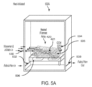
[0055] FIGS. 5A & 5B depicts further details of a chamber 630A
which may be used
interchangeably with any of the chambers described above, e.g., chambers 130
(FIG. 1) or 230
(FIG. 2). In the heat-initiated embodiment of FIG. 5A, the monomer and
initiator are fed into the
chamber 630B via inlet 530 and heated by a heated filament array 420, which
includes a metal
structure 421 that distributes heat for vapor phase polymerization 535 (which
is depicted in an
exaggerated mannerr as a mist of particles). The yarn enters at input 532 and
exits at output 538
and is coated with the in the manner described above. In one embodiment, a
quartz crystal
microbalance (QCM) sensor 534 is used to determine that the correct thickness
has been achieved.
[0056] In the embodiment of FIG. 5B, instead of heating the
monomer and initiator, a UV
lamp 540 is placed at the top of chamber 630B, and the UV light (wavelength
<400 nm) 544 shines
through the window 542 at the top of chamber 630B and interacts with the
monomer and initiator
for vapor phase polymerization 546.
[0057] FIG. 6A illustrates a print head 300A for producing
electrically conductive patterns
onto any substrate 612, such as a flat or smooth plastic, paper, transparent
conducting oxide or
metal oxide surface, or nonwoven, prewoven or knit fabric surface, in which
EDOT monomer and
solid oxidant, such as Fe(III) salts or Copper(II) salts, vapors are sprayed
to form PEDOT directly
on the surface. The print head 300A includes an initiator inlet 602 and a
monomer inlet 604 for
the aforementioned oxidant and monomer, or any other variation disclosed
herein, as well as a
carrier gas inlet 606, and a manifold 608 that distributes the gases to an
interior of the print head
where the polymerization 610 begins prior to deposition on the substrate 612
This print head is
capable of printing complexly patterned conductive polymer lines and shapes,
i.e. the shape of a
hand, and it can print in a resolution as small as 10 microns. The body of the
print head is in the
shape of a cylinder. It is made of alumina or another thermally stable ceramic
that has feedthroughs
for resistively heated filaments 620 such as tungsten and thermocouples for
controlling power
delivery and maintaining temperature. The heated filament coils within the
body of the print head
to heat the bottom of the EDOT reservoir, sidewalls, and tip of the funnel
that delivers the oxidant.
The EDOT monomer is held in a reservoir, and it can feature a carrier gas line
to help deliver
EDOT vapor to the substrate. The oxidant is contained in a reservoir above the
funnel section of
the ceramic body, and an auger screw can be incorporated to control the
delivery of oxidant to the
heated funnel section, which then leads to the substrate. The hottest part of
the funnel section is
14
CA 03173022 2022- 9- 22
WO 2021/194931
PCT/US2021/023412
near the tip, and this is achieved by having more wraps of the heated filament
closer to the tip. The
resistively heated filaments will heat the body of the ceramic causing the
EDOT monomer to
vaporize and the oxidant to sublimate. The two vapors will then flow out and
down, and they will
interact above the surface to coat it in PEDOT The height between the surface
of the substrate and
the tip of the print head can be 0.1-1.0mm.
100581 In the embodiment of FIG. 6A, system 300A is a heat
initiated print head for
printing an encapsulating polymer onto any flat or smooth plastic, paper,
transparent conducting
oxide or metal oxide surface, or nonwoven, prewoven or knit fabric surface.
This print head is an
inkjet printer head, e.g., less than 10 cm wide and located approximately 1-
10mm in distance from
the substrate surface. The printer head is equipped with nitrogen gas jets,
monomer feed, and
initiator feed. Nitrogen gas is used to help carry the monomer and initiator
vapors out of their
ampules, and the monomer and initiator ampules can have a similar setup as FIG
3B. The nitrogen
gas jets creates a vacuum space, such that the chemical reaction occurs in a
localized vacuum area
on the substrate. The monomer and initiator vapors are mixed before flowing
past the nichrome
filament, and they are flowed in this localized vacuum area because the
presence of oxygen inhibits
the polymerization. The vaporized monomer/initiator mix will flow past a
resistively heated
nichrome filament that is heated between 150-400 C before reaching the
substrate to initiate
radicals that in turn radicalize the monomer so it can polymerize the
encapsulating material on the
substrate surface. Openings for monomer/initiator are in the range of e.g., 10
to 100 micrometers
in diameter, in one embodiment
[0059] In the embodiment of FIG. 6B, system 300B is light
initiated. The print head of
system 300B would function similarly as 300A (see common reference numbers as
discussed
above), but instead of generating radicals using heated nichrome wires of
filament 620, it will
generate radicals using UV light (wavelength <400nm) introduced from UV lamp
540 via window
542. In this case, the nichrome filament 620 is not needed. The UV light will
flood the space
through which the monomer and initiator vapors will travel, the distance
between tip of the print
head and substrate, and the substrate. The substrate-facing part of the print
head would be made
up of a quartz glass such as to allow UV light (wavelength <400 nm) through.
CA 03173022 2022- 9- 22
WO 2021/194931
PCT/US2021/023412
[0060] With respect to the print head embodiment described above,
conventional print
heads are known for printing using liquid inks. For example, conventional
inkjet printer propel a
liquid ink onto paper in order to produce a pattern using either heat,
pressure, or a combination
thereof in a conventional manner that is well understood and well known to the
ordinary artisan in
the field. But conventional print heads are incapable of delivering two
components that are
supposed to react, and even further lack the concept of having an initiation
means, such as heat or
light, to cause such as reaction. Conventional print heads are designed for
speed, and printing onto
flat paper only, have no facility for initiating chemical reactions, and thus
cannot be used to create
an electrically conductive polymer coating as described herein. A person of
ordinary skill in the
art will understand that conventional ink jet printers include both one or
more print heads and a
control mechanism that allows the print heads, which include may include
numerous output
nozzles for different color inks, to move back and forth along a sheet of
paper in order to print the
required pattern. Such control mechanisms may be used with the present
technique so that the
presently described innovative print heads may move back and forth over any of
the types of
substrates described herein to form an electrically conductive and
encapsulated coating on those
substrates.
[0061] Advantageously, the presently disclosed vapor deposition
print head includes light
initiated or heat initiated polymerization of a monomer and an initiator so
that an electrically
conductive material such as PEDOT can be conformally deposited on a substrate
such as a yarn,
fiber, fabric or textile The print head can also include another nozzle from
which an encapsulating
material is delivered. The control mechanism can then time the delivery of the
materials so that
as the print head moves above the substrate, a fully encapsulated,
electrically conductive polymer
such as PEDOT is delivered to the substrate in whatever pattern is desired.
Because the vapor
phase polymerization can occur within a short distance such as a few
centimeters, the result is a
substrate that is conformally coated and encapsulated with the conductive
polymer.
[0062] Many examples of the utility of the present disclosure
have been contemplated by
the inventors, including heated gloves, hats, and other clothing, printed
circuits that are embedded
onto clothing to form wearable devices, etc. Various other applications of the
present disclosure
have been contemplated, including wearables that provide heat to a user,
monitor the users health
16
CA 03173022 2022- 9- 22
WO 2021/194931
PCT/US2021/023412
by measuring electric signals and temperatures, allow for mounting of other
components such as
blood pressure or oxygen sensors, etc.
100631 Therefore, and as discussed above, generally stated,
provided herein are a variety
of techniques for coating electrically conductive polymer onto flat or smooth
plastic, paper,
transparent conducting oxide or metal oxide surface, or nonwoven, prewoven or
knit fabric surface
that is encapsulated with an insulating material. The various components FIGS.
1-6B can be
rearranged or combined in different ways to construct systems for producing
the yarn, fiber or
fabric. For instance, any of the chambers 110, 120, 130, 210, 220, 230, 410,
520, 630A, or 630B
can be mixed and matched to provide a system in accordance with the present
disclosure. In
addition, the process details discussed with respect to the chamber based
embodiments are also
applicable to the printer/spray head embodiments 300A, 300B and 300C. In
addition, certain well-
known details have only been touched upon, such as the use of an inert carrier
gas to carry the
chemicals through the process chamber, the use of vacuum pumps to maintain a
vacuum, the use
of motors and other details of the spooling mechanism, etc., that a person of
ordinary skill in the
art would understand.
100641 The fact that one or more specific embodiments for
coating, cleaning and
encapsulating have been used to illustrate the concepts of the present
technique are not meant to
limit the disclosure in any manner. Indeed, as noted above, the concepts
disclosed herein are not
limited to textiles, yams, fibers or fabrics For example, many other
applications of the different
processes described herein have been envisaged by the inventors and are
included within the scope
of this disclosure. The presentation of a specific set of claims herein is not
meant to limit scope,
but is only done to illustrate some of the example embodiments which are
covered by this
disclosure. For example, the techniques described herein may be scaled in size
from a large factory
embodiment measuring many yards in each direction down to a smaller table-top
apparatuses that
are only a few feet in size. In addition to fiber, fabric, and yarn
embodiments, the present
disclosure could be used for producing circuits that are printed on any of the
substrates identified
above, and the coating and encapsulation process can be used to form the
conductive lines of the
circuit. By adding other electrical or semiconductor elements in a manner
known in the art, the
end product would be a wearable or non-wearable circuit or electronic device
that could be
17
CA 03173022 2022- 9- 22
WO 2021/194931
PCT/US2021/023412
conformed to any surface or configuration, providing great advantages compared
to flat circuit
boards presently used in the field.
18
CA 03173022 2022- 9- 22