Note: Descriptions are shown in the official language in which they were submitted.
WO 2021/202093
PCT/US2021/022412
OPTICAL MICRORESONATOR ARRAY DEVICE FOR ULTRASOUND SENSING
CROSS-REFERENCE TO RELATED APPLICATIONS
100011 This application claims priority to U.S. Patent Application Serial No.
63/001,738 filed
March 30, 2020, which is incorporated herein in its entirety by this
reference.
TECHNICAL FIELD
100021 The present disclosure generally relates to the field of ultrasound,
and in particular to
methods and devices that enable ultrasound sensing using an array of optical
microresonators.
BACKGROUND
100031 Ultrasound sensing is used in various industries including medical
imaging, due to a
number of advantages. For example, ultrasound sensing utilizes ultrasound
signal which has a
remarkable penetration depth. Moreover, ultrasound imaging is known to be an
advantageously
non-invasive form of imaging, as it is based on non-ionizing radiation.
100041 Conventional ultrasound sensing uses piezoelectric materials such as
lead-zirconate-
titanate (PZT), polymer thick film (PTF) and polyvinylidene fluoride (PVDF).
However, some
of the challenges associated with use of piezoelectric properties of these
materials include high
operation voltage requirements, a high electric field requirement (which may
cause breakdown
and failure), a non-linear response with high hysteresis, and limited angle of
detection. Thus,
there is a need for new and improved devices and methods for ultrasound
sensing.
SUMMARY
100051 Generally, in some embodiments, an apparatus may include one or more
(e.g., a
plurality of) optical fibers, one or more optical waveguides, and a plurality
of resonator nodes
arranged in an array of sensing locations. Each resonator node may include an
optical coupling
between an optical waveguide and an optical fiber that has a set of resonant
frequencies at a
respective sensing location. Each resonator node may be further configured to
communicate a
set of signals corresponding to a shift in the set of resonant frequencies in
the optical fiber at the
respective sensing location. In some embodiments, each optical fiber may have
the same or
substantially similar cross-sectional geometry and/or material uniformity,
such that the optical
CA 03174131 2022- 9- 29
WO 2021/202093
PCT/US2021/022412
fibers may have the same or substantially similar set of resonant frequencies.
By leveraging such
uniform material characteristics (e.g., utilizing optical fibers produced in
bulk), an ultrasound
sensing system including such an apparatus may be more easily mass-produced in
a cost-
efficient and consistent manner and have more consistent, predictable
performance.
[0006] In some embodiments, the one or more optical fibers may be configured
to receive
multiple ultrasound echoes. Furthermore, the one or more optical fibers may be
configured to
experience the shift in the set of resonant frequencies in response to the
multiple ultrasound
echoes. In some embodiments, the one or more optical waveguides are configured
to propagate a
set of signals corresponding to the at least one shift in the set of resonant
frequencies to an
optical detector.
100071 In some embodiments, the one or more optical waveguides may include one
or more
tapered optical fibers or one or more integrated photonic waveguides (e.g., a
silicon photonic
waveguide). The one or more tapered optical fibers may be in a polymer
structure.
100081 The one or more optical fibers may be arranged perpendicular to the one
or more
optical waveguides. For example, in some embodiments, the one or more optical
fibers maybe
arranged linearly at a predetermined equidistance from each other and
perpendicular to the one
or more tapered optical fibers. Furthermore, the one or more optical fibers
and the one or more
optical waveguides may be arranged in a rectangular grid.
[0009] In some embodiments, the one or more optical waveguides may be coupled
to a light
source, and the light source may propagate the light in the one or more
optical waveguides. For
example, the light source may include a broadband light source or a tunable
laser source.
[0010] The one or more optical fibers and the one or more optical waveguides
may be
arranged in any suitable manner that enables optical coupling at each
resonator node. For
example, in some embodiments, an optical fiber may be in physical contact with
an optical
waveguide at a resonator node Alternatively, in embodiments there may be a
short separation
gap (e.g., about a 1 p.m separation or less) between an optical fiber and an
optical waveguide at a
resonator node. Furthermore, the optical waveguides and the optical fibers may
be spaced apart
in any suitable manner. For example, in some embodiments, the distance between
optical
waveguides of the one or more optical waveguides may be at least about 20
times the
2
CA 03174131 2022- 9- 29
WO 2021/202093
PCT/US2021/022412
wavelength of the light from the light source. In some embodiments, the
distance in between
optical fibers of the one or more optical fibers may be less than about 3
times the wavelength of
the light.
[0011] Generally, in some embodiments, a method for ultrasound sensing may
include
receiving at one or more optical waveguides, via multiple (e.g., more than
one) resonator nodes,
a first set of signals corresponding to a first set of whispering gallery
modes that propagate along
the circumference of one or more optical fibers The method may further include
receiving at the
one or more optical waveguides, via the multiple resonator nodes, a second set
of signals
corresponding to a second set of whispering gallery modes that propagate along
the
circumference of each optical fiber. In some embodiments, the second set of
whispering gallery
modes may propagate in response to the one or more optical fibers receiving
multiple ultrasound
echoes. The method may further include detecting a set of differences between
the first set of
signals and the second set of signals. The method may further include
calculating a magnitude of
each ultrasound echo at each resonator node based at least in part on the
first set of signals, the
second set of signals, and/or the set of differences. The method may further
include associating
the magnitude of each ultrasound echo to a sensing location of each resonator
node. In some
embodiments, the method may further include transmitting multiple ultrasound
signals using
multiple piezoelectric elements. The method may further include receiving the
multiple
ultrasound echoes corresponding to the multiple ultrasound signals at the one
or more optical
fibers, the multiple resonator nodes may be configured to perform a synthetic
aperture (SA)
operation or a compressed sensing (CS) operation.
[0012] In some embodiments, the one or more optical fibers may include a
plurality of optical
fibers having the same or substantially similar cross-sectional geometry and
material so as to
have the same or substantially similar sets of resonance frequencies In some
embodiments, the
one or more optical fibers may be perpendicular to the one or more optical
waveguides. In some
embodiments, the one or more optical waveguides may include one or more
tapered optical
fibers and/or one or more integrated photonic waveguides, or another suitable
waveguide that
may be coupled to a light source so as to propagate light from the light
source. In some
embodiments, the one or more optical fibers and/or the one or more optical
waveguides may be
in a polymer structure.
3
CA 03174131 2022- 9- 29
WO 2021/202093
PCT/US2021/022412
[0013] The one or more optical fibers and the one or more optical waveguides
may be
arranged in any suitable manner that enables optical coupling at each
resonator node. For
example, in some embodiments, an optical fiber may be in physical contact with
an optical
waveguide at a resonator node. Alternatively, in embodiments there may be a
short separation
gap (e.g., about a 1 p.m separation or less) between an optical fiber and an
optical waveguide at a
resonator node. Furthermore, the optical waveguides and the optical fibers may
be spaced apart
in any suitable manner. For example, in some embodiments, the distance between
optical
waveguides of the one or more optical waveguides may be at least about 20
times the
wavelength of the light from the light source. In some embodiments, the
distance in between
optical fibers of the one or more optical fibers may be less than about 3
times the wavelength of
the light.
100141 Generally, in some embodiments, an apparatus may include one or more
optical fibers
and one or more optical waveguides that are optically coupled to the one or
more optical fibers
at multiple resonator nodes. The circumference of each optical fiber may be
configured to
propagate a first set of whispering gallery modes. In some embodiments, the
one or more optical
fibers communicate to the one or more optical waveguides a first set of
signals corresponding to
the first set of whispering gallery modes. The one or more optical waveguides
may be
configured to propagate the first set of signals to at least one optical
detector.
100151 In some embodiments, the one or more optical fibers may include a
plurality of optical
fibers having the same or substantially similar cross-sectional geometry and
material so as to
have the same or substantially similar sets of resonance frequencies In some
embodiments, the
one or more optical fibers may be perpendicular to the one or more optical
waveguides. In some
embodiments, the one or more optical waveguides may include one or more
tapered optical
fibers and/or one or more integrated photonic waveguides, or another suitable
waveguide that
may be coupled to a light source so as to propagate light from the light
source. In some
embodiments, the one or more optical fibers and/or the one or more optical
waveguides may be
in a polymer structure.
100161 The one or more optical fibers and the one or more optical waveguides
may be
arranged in any suitable manner that enables optical coupling at each
resonator node. For
example, in some embodiments, an optical fiber may be in physical contact with
an optical
waveguide at a resonator node. Alternatively, in embodiments there may be a
short separation
4
CA 03174131 2022- 9- 29
WO 2021/202093
PCT/US2021/022412
gap (e.g., about a 1 urn separation or less) between an optical fiber and an
optical waveguide at a
resonator node. Furthermore, the optical waveguides and the optical fibers may
be spaced apart
in any suitable manner. For example, in some embodiments, the distance between
optical
waveguides of the one or more optical waveguides may be at least about 20
times the
wavelength of the light from the light source. In some embodiments, the
distance in between
optical fibers of the one or more optical fibers may be less than about 3
times the wavelength of
the light.
[0017] In some embodiments, the one or more optical fibers are configured to
receive
multiple ultrasound echoes and propagate a second set of whispering gallery
modes in response
to the multiple ultrasound echoes. The one or more optical fibers are
configured to communicate
to the one or more optical waveguides a second set of signals corresponding to
the second set of
whispering gallery modes. In some embodiments, the one or more optical
waveguides are
configured to propagate the second sets of signals to the at least one optical
detector.
[0018] In some embodiments, the one or more optical fibers may be configured
to
communicate, through the multiple resonator nodes, to the one or more optical
waveguides a set
of signals corresponding to a difference between the first set of whispering
galley modes and the
second set of whispering gallery modes. For example, the difference between
the first set of
whispering gallery modes and the second set of whispering gallery modes
includes at least one
of a shift in a resonant frequency of the optical fiber and/or an attenuation
of a resonance of the
one or more optical fibers.
BRIEF DESCRIPTION OF THE DRAWINGS
[0019] FIG. lA is a schematic description of an exemplary optical
microresonator array.
[0020] FIG. 1B is a schematic description of an exemplary optical
microresonator array.
[0021] FIG. 1C is a schematic description of an exemplary optical
microresonator array.
[0022] FIG. 1D is a schematic description of an exemplary optical
microresonator array.
CA 03174131 2022- 9- 29
WO 2021/202093
PCT/US2021/022412
[0023] FIG. 2A is a schematic description of an exemplary method of packaging
an optical
microresonator array.
[0024] FIG. 2B is a schematic description of an exemplary method of packaing
an optical
microresonator array.
100251 FIG. 3A is a schematic description of an exemplary optical
microresonator array.
[0026] FIG. 3B is a schematic description of an exemplary optical
microresonator array.
[0027] FIG. 3C is a schematic description of an exemplary optical
microresonator array.
[0028] FIG. 4 is a schematic description of an exemplary method of sensing a
set of
ultrasound echoes using an optical microresonator array device.
[0029] FIG. 5 is a schematic description of an exemplary method of measuring
optical
response of an optical microresonator array device
[0030] FIG. 6 is a schematic description of an exemplary method of measuring
optical
response of an optical microresonator array device.
[0031] FIGS. 7 and 8 are schematic descriptions of an exemplary ultrasound
probe.
DETAILED DESCRIPTION
[0032] Non-limiting examples of various aspects and variations of the
invention are described
herein and illustrated in the accompanying drawings.
[0033] Exemplary optical microresonator arrays and methods of making the same
are
described herein. Furthermore, as described herein, such optical
microresonator arrays may be
combined to form optical microresonator arrays with high quality factor and
various other
beneficial features as described below, for use in applications such as
ultrasound sensing and/or
ultrasound imaging.
Optical microresonator arrays
100341 Described herein are optical microresonator arrays suitable for high
sensitivity
applications including high sensitivity acousto-optic sensing systems. For
example, as shown in
6
CA 03174131 2022- 9- 29
WO 2021/202093
PCT/US2021/022412
FIG. 1A, an exemplary optical microresonator array 100A may include a set of
(e.g., a plurality
of) optical fibers 103A, a set of (e.g., a plurality of) optical waveguides
102A, and multiple
resonator nodes 104A arranged in an array of sensing locations. Each resonator
node 104A may
comprise an optical coupling between an optical waveguide and an optical fiber
at a respective
sensing location. Each optical fiber may have a set of resonant frequencies,
and each resonator
node 104A may be further configured to communicate a set of signals
corresponding to at least
one shift in the set of resonant frequencies in the optical fiber at the
respective sensing location.
At each resonator node, the cross-section of the optical fiber may function as
an optical
microresonator (e.g., whispering gallery mode microresonator) configured to
communicate a set
of signals corresponding to the at least one shift in the set of resonant
frequencies in the optical
fiber. These signals are associated with the respective sensing location for
that resonator node.
[0035] Each optical microresonator of the optical microresonator arrays
includes a closed loop
of a transparent medium that allows some permitted frequencies of light to
continuously
propagate inside the closed loop, and to store optical energy of the permitted
frequencies of light
in the closed loop. As such, the optical microresonator permits a propagation
of whispering
gallery modes (WGMs) traveling around the optical microresonator and
corresponding to the
permitted frequencies to circulate the circumference of the optical
microresonator. Each mode
from the WGMs may, for example, correspond to propagation of a frequency of
light from the
permitted frequencies of light.
[0036] The optical microresonator arrays described herein have high
sensitivity due at least in
part on having high quality factors, in that they advantageously allow the
permitted frequencies
of light to stay in the closed loop of the optical microresonator array for a
long period of time
The permitted frequencies of light and the quality factor of the optical
microresonator array
described herein may be based at least in part on geometrical parameters of
the optical
microresonator array, refractive index of the transparent medium, and
refractive indices of an
environment surrounding the optical microresonator array.
[0037] As further described herein, the optical microresonator arrays may be
configured to
receive light, to transmit light, and to be useful in practice (e.g., for an
ultrasound imaging or
other sensing application in an acousto-optic system). Acousto-optic systems
based on the
optical microresonator arrays may directly measure ultrasonic waves through
the photo-elastic
effect and/or physical deformation of the optical microresonator arrays in
response to the
7
CA 03174131 2022- 9- 29
WO 2021/202093
PCT/US2021/022412
ultrasonic waves (e.g., ultrasonic echoes). For example, in the presence of
ultrasonic (or any
pressure) waves, the WGMs traveling an optical microresonator arrays may
undergo a set of one
or more spectral shifts caused by changes in the refractive index and/or shape
of the optical
microresonator arrays. The spectral change can be easily monitored and
analyzed in spectral
domain and light transmission intensity to and from the optical microresonator
array. Additional
spatial and other information can furthermore be derived by monitoring and
analyzing shifting
WGMs among multiple optical microresonator arrays
100381 In some embodiments, the optical microresonator arrays may include
optical fibers
having identical or substantially similar cross-sectional characteristics
(e.g., cross-sectional
geometry and/or material properties) along their length and/or with respect
each other, as further
described herein. Accordingly, the availability of bulk-produced optical
fibers may be leveraged
to manufacture optical microresonator arrays in an efficient, highly
reproducible manner suitable
for mass production. Furthermore, using such similar, bulk-produced optical
fibers (and/or
optical waveguides) in the optical microresonator arrays may result in more
consistent, reliable
performance in ultrasound sensing. Thus, the optical microresonator arrays
described herein
provide several advantages over microresonator arrays formed from conventional
techniques, in
which standalone microresonators must be painstakingly individually formed
before being
combined into an array, and yet may exhibit inconsistent or unreliable
performance as the result
of variability among the individual microresonators and/or require complex
micro- or
nanofabrication techniques to trim individual microresonator resonance
wavelengths.
Furthermore, for embodiments of the optical microresonator array having
optical fibers with
identical or very close WGM resonance conditions and resonant frequencies, it
may be possible
to use a single frequency laser or other single frequency light source to
probe or excite all the
WGMs in the optical microresonator array simultaneously, thereby simplifying
operation of the
sensing microresonator array.
100391 Alternatively, in some embodiments at least some of the optical fibers
may have
varying known cross-sectional characteristics (e.g., different radii,
different material profiles)
thus exhibit different resonance frequencies which are accounted for during
analysis of the
signals obtained as the result of shifting WGMs.
8
CA 03174131 2022- 9- 29
WO 2021/202093
PCT/US2021/022412
Optical fibers and optical waveguides
[0040] The set of optical fibers 103A in the optical microresonator array may
be made of a
material (e.g., glass, polymer, crystal, etc.) transparent to a frequency of
light propagating inside
the set of optical fibers. The set of optical fibers 103A may include, for
example, a set of one or
more single model optical fibers, a set of one or more multimode optical
fibers, a set of one or
more graded index optical fibers, a set of one or more step index optical
fibers, a set of one or
more polarization maintaining optical fibers, and/or any optical fiber that is
suitable for
supporting a whispering gallery mode at its circumference. In some
embodiments, the set of
optical fibers may include commercially available fibers that collectively
have the same or
significantly similar properties in term of size, refractive index, and/or
resonance wavelength,
for example. For example, a set of single mode optical fibers can have a very
uniform material
index of 1.5 and a diameter of 125 pm at any perpendicular cross-section of
the set of single
mode optical fibers.
[0041] In some embodiments the set of optical fibers 103A may be selected to
and/or etched to
have a small radius. The smaller radius of the set of optical fibers results
in larger free spectral
range of the set of resonant frequencies. As a result, the spectral density of
the resonance modes
supported by the radius of the set of optical fibers 103A is reduced, which
may improve the
dynamic range of the sensing performance of the optical microresonator array
100A.
[0042] In some embodiments, the set of optical waveguides 102A may include a
set of
integrated photonic waveguides made of glass, silicon, silicon nitride, and/or
any material
transparent to a frequency of light propagating inside the set of optical
fibers. For example, the
set of optical waveguides 102A may include a set of strip waveguides, slot
waveguides, slab
waveguides, strip-loaded slot waveguides, photonic crystal waveguides, and/or
any integrated
photonic waveguides that is suitable for supporting propagation of light
across the length of the
optical microresonator array.
[0043] Additionally or alternatively, the set of optical waveguides 102A may
include a set of
tapered optical fibers produced from optical fibers. For example, at least a
portion of the set of
optical waveguides 102A can be produced from a set of single model optical
fibers, multimode
optical fibers, graded index optical fibers, step index optical fibers,
polarization maintaining
optical fiber, and the like. Generally, in some embodiments, the set of
tapered optical fibers may
9
CA 03174131 2022- 9- 29
WO 2021/202093
PCT/US2021/022412
be produced by gently stretching the optical fibers while it is heated. In
doing so, the optical
fibers become thinner over some length. Additionally or alternatively, in some
embodiments, at
least a portion of the set of tapered fibers may be produced by etching (e.g.,
using wet etch) a
cladding of optical fibers in whole or in part.
100441 In some embodiments, the set of optical fibers and/or the set of
tapered optical fibers
can be etched to reduce their size. For example, the set of optical fibers
and/or the set of tapered
optical fibers can be etched using a chemical solution (e.g., hydrochloric
acid) to reduce their
length and/or radius. A predetermined portion of the set of optical fibers and
or the set of tapered
optical fibers may be exposed to chemical solution, so that only the part
exposed to the chemical
solution is etched.
[0045] The system may further include one or more light sources. For example,
the set of
optical waveguides 102A may be coupled to a set of one or more light sources
such that input
light 101A from the set of light sources into the set of optical waveguides
102A and into the
optically-coupled optical fibers 103A. Light then propagates along the
azimuthal angle of each
optical fiber to excite the WGM of the resonator nodes as further described
herein. Additionally,
light can additionally couple out from the optical fibers 103A and back into
the optical
waveguides 102A.
100461 The one or more light sources can include a broadband light source, a
tunable laser
source, an optical frequency comb (OFC) laser source using either a digital
modulating method
or using a Kerr four-wave mixing (FWM) method, and/or any other light sources
suitable for the
operation frequency band of the optical microresonator array 100A. In some
embodiments, the
set of one or more light sources can include a single frequency light source
configured to
propagate light 101A with identical spectral characteristics into the set of
optical waveguides
102A. Tn some embodiments, at least one light source may include a fiber laser
source that
launch input light 101A directly into the set of optical fibers which may
couple the input light
101A into a set of integrated photonic waveguides. In some embodiments, the
set of light
sources may include a set of chip-based laser sources that launch the set of
input lights 101A
directly to the set of integrated photonic waveguides. The set of integrated
photonic waveguides
may then be configured to couple the set of input lights into a set of tapered
fibers. Furthermore,
in some embodiments, the one or more light sources may be coupled into a slab
or planar
waveguide as described in further detail below.
CA 03174131 2022- 9- 29
WO 2021/202093
PCT/US2021/022412
[0047] The optical fibers and optical waveguides may be arranged in any of
various suitable
manners. For example, as shown in FIG. 1A, an optical microresonator array
100A may include
tapered optical fibers (functioning as optical waveguides 102A) overlaid over
optical fibers
103A to form a plurality of resonator nodes 104A. As described in further
detail below,
alternatively at least a portion of optical fibers 103A may be overlaid over
the tapered optical
fibers (waveguides 102A).
100481 As another example, one or more optical fibers may be arranged over an
integrated
photonic waveguide platform, such as a silicon photonic platform, a silicon
nitride platform,
and/or the like, such as that shown in FIGS. 1B-1D. FIG. 1B is a schematic
description of an
exemplary integrated photonic optical waveguide array 100B. In some
embodiments, the
integrated photonic platform may include a substrate 107B (e.g., silicon,
silica, silicon nitride,
and/or the like), a buried oxide layer 106B, and other integrated photonic
components. The
optical waveguide array 100B can be coupled to a set of one or more light
sources. In some
embodiments, the set of light sources can be a fiber-coupled light source or
other light source
emitting light 101B into a fiber that is aligned vertically to an on-chip
grating coupler 102B. The
grating coupler 102B combined with other integrated photonic components (e.g.,
a multimode
interference device 103B) may couple the light into the optical waveguide
array 100B with one
or more optical waveguides 108B. For example, as shown in FIG. 1B, input light
from a single
light source may be coupled into multiple optical waveguides 108B via a
dividing or branching
pattern. In some embodiments, at least a portion of the optical waveguide
array 100B may be
coated with the encapsulation layer 105B (e.g., spin coated with a matching
polymer) while
other parts of the optical waveguide array 100B may remain uncoated with the
encapsulation
layer 105B (e.g., by selectively etching the encapsulation layer).
100491 FIG. 1C is a schematic description of another exemplary optical
microresonator array
100C in which multiple resonator nodes 104C are positioned at a set of sensing
locations. The
optical microresonator array 100C may include an optical waveguide array 102C
with multiple
optical waveguides 108C arranged in an integrated planar optical platform
(similar to the optical
waveguide array 100B as described above with respect to FIG. 1B) and a set of
optical fibers
103C that are optically coupled to the optical waveguide array 102C at the set
of sensing
locations to establish the multiple resonator nodes 104C. Each resonator node
may have a
predetermined position with respect to other resonator nodes for determining
location of an
11
CA 03174131 2022- 9- 29
WO 2021/202093
PCT/US2021/022412
acoustic echo detected by the resonator node. Similar to that described above
with respect to
FIG. 1B, the optical waveguide array 102C can include integrated photonic
waveguides
fabricated on a substrate 105C. In some embodiments, the optical waveguide
array may include
multiple light sources that couple input light at input waveguides 101C, each
of which may be
connected in turn to multiple optical waveguides 108C (e.g. via a beam
splitter or a fiber
coupler). The embodiment shown in FIG. 1C includes a single light input for
three optical
waveguides; however, it should be understood that other embodiments may
include any suitable
ratio of light inputs to optical waveguides 108C (e.g., about 1:2, 1:3, 1:4,
etc.). Each of the
optical waveguides 108C in the optical waveguide array 102C may be
perpendicular to a set of
optical fibers 103C to produce multiple resonator nodes 104C. As further
described herein, the
multiple resonator nodes 104C may couple the light into the set of optical
fibers 103C to
propagate a set of WGMs and generate a set of optical signals into the optical
waveguide array
102C. The optical waveguide array may be connected to a set of photodetectors
and a
multichannel optical spectrum analyzer to characterize the set of optical
signals for ultrasound
sensing.
100501 FIG. 1D is a schematic description of another optical microresonator
array 100D in
which a set of resonator nodes 104D are positioned at a set of sensing
locations. The optical
microresonator array 100D may include an optical waveguide array 102D with
multiple optical
waveguides 108D arranged in an integrated planar optical platform (similar to
the optical
waveguide array 100B as described above with respect to FIG. 1B) and a set of
optical fibers
103D that are optically coupled to the optical waveguide array 102D at the set
of sensing
locations to establish the multiple resonator nodes 104D. Each resonator node
may have a
predetermined position with respect to other resonator nodes for determining
location of an
acoustic echo detected by the resonator node. As shown in FIG. ID each optical
waveguide
108D from the optical waveguide array 102D can be optically coupled to a
respective light input
101D (each of which may, for example, be coupled to a respective light source,
or at least some
of the light inputs may source light from a common light source). In other
words, the ratio of
light inputs to optical waveguides 108D may be 1:1). Each of the optical
waveguides 108D in
the optical waveguide array 102D may be perpendicular to a set of optical
fibers 103D to
produce multiple resonator nodes 104D. As further described herein, the
multiple resonator
nodes 104D may couple the light into the set of optical fibers 103D to
propagate a set of WGMs
and generate a set of optical signals into the optical waveguide array 102D.
The optical
12
CA 03174131 2022- 9- 29
WO 2021/202093
PCT/US2021/022412
waveguide array may be connected to a set of photodetectors and a multichannel
optical
spectrum analyzer to characterize the set of optical signals for ultrasound
sensing.
Resonator nodes
100511 The system may include a set of resonator nodes at various sensing
locations where
optical waveguides and optical fibers are optically coupled. For example, FIG.
lA is a schematic
illustration of an optical microresonator array 100A in which resonator nodes
104A are
positioned at sensing locations where the optical fibers 103A and the optical
waveguides 102A
are optically coupled. Each resonator node may have a predetermined position
with respect to
other optical microresonators for determining location of a detected acoustic
echo
100521 In some embodiments, the input light 101A may couple to the set of
optical fibers
103A, such that a set of whispering gallery modes (WGMs) propagate around the
inner
circumference of the optical fibers 103A at the multiple resonator nodes 104A.
Each resonator
node may have an associated sensing coordinate. The multiple resonator nodes
104A may
receive a set of ultrasound echoes that are spatially distributed with various
intensities across the
multiple resonator nodes 104A of the optical microresonator array. In some
embodiments, each
resonator node may have a predetermined position with respect to other
resonator nodes for
determining location of an acoustic echo detected by the resonator node. In
some other
instances, each resonator node may have characteristics geometry and/or
material refractive
index associated to the resonator node that can distinguish an optical
response of the resonator
node from other resonator nodes. Sensing using the resonator nodes is
described in further detail
below.
100531 The resonator nodes 104A may be arranged in various suitable kinds of
arrays and in
various suitable manners with respect to the set of optical fibers and the set
of optical
waveguides. In some embodiments, the set of optical fibers 103A may be
perpendicular to the
optical waveguides 102A so as to allow light from the optical waveguides 102A
to circulate
around the cross-sections of the optical fibers 130A. For example, the optical
fibers may be
arranged perpendicular to the optical waveguides using an alignment procedure.
The alignment
procedure may include propagating a first set of lights having a first set of
intensities to the set
of optical waveguides 102A. The alignment procedure may further include
detecting a second
set of light having a second set of intensities. The alignment procedure may
include adjusting a
13
CA 03174131 2022- 9- 29
WO 2021/202093
PCT/US2021/022412
set of angles between the set of optical fibers 103A and the set of optical
waveguides 102A (e.g.,
by using a high precision positioning system) to maximize the second set of
intensities. In one
example, the adjustment of the set of angles is to achieve a perpendicular
angle between each
optical fiber and optical waveguide. In some instances, the alignment
procedure may result in a
gap between an optical fiber and an optical waveguide to achieve a coupling
condition that
results in highest power coupled into the resonator node. In some other
instances, an optical fiber
may be in physical contact with an optical waveguide so as to improve the
stability of the
coupling condition. The perpendicular angle between the set of optical fibers
103A and the set of
optical waveguides 102A can allow for a light to couple from the set of
optical fibers 103A to
couple to the set of optical waveguides 102A, and vice versa. In some
embodiments, the
alignment procedure may include verifying perpendicularity between the set of
optical fibers
103A and the set of optical waveguides 102A by verifying the light coupling
between the optical
fibers and optical waveguides.
100541 In some embodiments, the resonator nodes may be arranged in a grid such
as a
rectangular array, formed from the optical fibers and the optical waveguides
arranged in a grid.
For example, the set of waveguides may also be arranged parallel and
equidistant from each
other, and the optical fibers may be arranged parallel and equidistant from
each other and
perpendicular to the set of waveguides. However, in some embodiments the
optical fibers may
be irregularly spaced apart and/or the waveguides may be irregularly spaced
apart.
[0055] Although in some embodiments the optical microresonator array may
include multiple
optical waveguides and multiple optical fibers such as that shown in FIG. IA,
it should be
understood that multiple resonator nodes may also be formed from only a single
optical
waveguide, or only a single optical fiber.
[0056] For example, as shown in FTG 3A, in some embodiments the optical
microresonator
array may include multiple resonator nodes formed by a single optical
waveguide 302A optically
coupled to multiple optical fibers 303A and 303A' at multiple sensing
locations. In some
instances, a set of light with multiple various wavelengths may propagate in
the single optical
waveguide 302A. In some other instances, a single wavelength of light may
propagate in the
single optical waveguide 302A. In some other instances, broadband light 301A
may propagate in
the single optical waveguide 302A. The single optical waveguide 302A may be
perpendicular to
and optically coupled to the optical fibers 303A and 303A' at multiple
separate sensing locations
14
CA 03174131 2022- 9- 29
WO 2021/202093
PCT/US2021/022412
on the length of the optical waveguide, thereby forming first and second
resonator nodes 304A
and 304A'. It should be understood that although two resonator nodes are
illustrated in FIG. 3A,
any suitable number of resonator nodes may be formed along a single optical
waveguide by
coupling any suitable number of optical fibers (e.g., three, four, five, or
more, etc.) to the optical
waveguide. Light input 301A may be coupled into and propagated around optical
fibers 303A
and 303A' respectively to excite the WGMs at the resonator nodes 304A and
304A',
respectively. Optical signals embodying WGMs and any shifts in WGMs may then
be coupled
out at the resonator nodes to the optical fibers and provided as output light
305A.
100571 As another example, as shown in FIG. 3B, in some embodiment, the
optical
microresonator array may include multiple resonator nodes formed by multiple
optical
waveguides 302B and 302B' coupled to a single optical fiber 303B at multiple
sensing locations.
In some instances, a first input light 301B and/or a second input light 301B'
each having various
wavelengths may propagate in each of the optical waveguides. In some other
instances, a first
single wavelength light 301B may propagate in one optical waveguide (e.g.,
optical waveguide
302B) and a second single wavelength light 301B' may propagate in another
optical waveguide
(e.g., optical waveguide 302B'). The optical waveguide 302B and an optical
waveguide 302B'
may be perpendicular to and optically coupled to a single optical fiber 303B
at multiple separate
sensing locations on the length of the optical fiber, thereby forming first
and second resonator
nodes 304B and 304B'. In some embodiments, the optical waveguide 302B and an
optical
waveguide 302B' may be identical in radii and material uniformity profiles,
and therefore
demonstrate identical WGMs and resonant frequencies at a set of resonator
nodes 304B and
304B. It should be understood that although two resonator nodes are
illustrated in FIG. 3B, any
suitable number of resonator nodes may be formed along a single optical fiber
by coupling any
suitable number of optical waveguides (e.g., three, four, five, or more, etc.)
to the optical fiber.
100581 Light input 301B and 301B' may be coupled into and propagated along
optical fiber
303B to excite the WGMs at the resonator nodes 304B and 304B', respectively.
Optical signals
embodying WGMs and any shifts in WGMs may then be coupled out at the resonator
nodes to
the optical fibers and provided as output light 305B and 305B'.
CA 03174131 2022- 9- 29
WO 2021/202093
PCT/US2021/022412
Sensing at resonator nodes
100591 For simplicity, sensing at the resonator nodes in the optical
microresonator array is
described below with respect to a single resonator node 304C as shown in FIG.
3C. The
resonator node 304C at a sensing location is formed when an optical waveguide
301C is aligned
and positioned so as to be optically coupled to a single optical fiber 303C.
Across an optical
microresonator array, multiple resonator nodes may be located at multiple
sensing locations or
coordinates. For example, in some embodiments the sensing location may be
located at the
intersection of the optical waveguide and the optical fiber.
100601 The optical waveguide 302C may be located on top of the optical fiber
303C or at the
bottom of the optical fiber 303C (or at any suitable tangent or laterally
offset from a tangent by a
separation gap). The optical waveguide 302C may be optically coupled to the
optical fiber 303C
at any location along the length of the single optical fiber 303C. The
longitudinal axis of the
optical waveguide 302C may be perpendicular to the longitudinal axis of the
optical fiber 303C.
The optical fiber 303C may be characterized with predetermined geometrical
features and
material features such as, for example, fiber radius, fiber surface roughness,
and/or fiber material
refractive index, each of which can affect an impedance, a scattering loss,
and/or an absorption
loss of the single optical fiber 303C that impacts the set of signals provided
by the resonator
node.
100611 Additionally, generally, the resonator node 304C has a characteristic
set of resonant
frequencies determined by geometrical properties and material properties of
the features located
at the sensing location. These geometrical and material properties at the
sensing location may be
impacted by a set of ultrasound echoes received at the sensing location,
thereby shifting the
resonant frequencies and/or attenuating a resonant peak or dip of the set of
resonant frequencies
of the resonator node 304C. Considering multiple resonator nodes across the
entire optical
microresonator array, received ultrasound echoes may impact the geometrical
properties and/or
material properties of multiple resonator nodes with different intensities at
different sensing
coordinates. Therefore, the ultrasound echoes may shift the set of resonant
frequencies and/or
attenuate a resonant peak/dip of the set of resonant frequencies of the
multiple resonator nodes
by various amounts that are indicative of different intensities of the set of
ultrasound echoes.
16
CA 03174131 2022- 9- 29
WO 2021/202093
PCT/US2021/022412
[0062] During use in sensing, the optical waveguide 302C may receive and
propagate light
301C from a light source. The light may, for example, be a single wavelength
light (e.g., a 532
nanometer laser), a broadband light (e.g. an Erbium-doped fiber amplifier),
and/or a multi-
wavelength light (e.g. a frequency comb). The light may be coupled to the
optical fiber 304C at
the resonator node 304C to excite a set of WGMs propagating azimuthally around
the
circumference of the optical fiber. The set of WGMs may result in a set of
signals 305C in the
optical waveguide 302C. The set of signals may include a set of resonance
features that are
characteristic of the single resonator node 304C, the single optical waveguide
302C, and/or the
single optical fiber 303C.
[0063] The single resonator node 304C may then receive a set of ultrasound
echoes that
mechanically vibrate the optical waveguide 302C, the optical fiber 303C, the
resonator node
304C, and/or the material inside and/or outside these components. Accordingly,
the geometrical
features and/or material refractive index of the optical waveguide 302C, the
optical fiber 303C,
the resonator node 304C, and/or the material inside and/or outside these
components may
experience a change associated with a change in the WGMs for the resonator
node. The change
could be small or large compared to default value of each geometrical feature
and/or material
refractive index. Even a small change in each geometrical feature and/or
material refractive
index can significantly impact the resonance features and result in a
detectable signal. In one
illustrative example, a change in refractive index by An = 0.01 of the single
optical fiber 303C
may be two orders of magnitude smaller than the refractive index n = 1.5 of
the single optical
fiber 303C. This change in refractive index, however, may be sufficient to
shift the resonance
features by a frequency amount comparable to the full-width at half maxima of
the resonance
feature.
[0064] In other words, a set of one or more shifts in resonance features in
response to receipt
of ultrasound echoes may correspond to a shift in propagation of a set of
optical signals (e.g.,
relating to the difference between a first set of WGMs and a second set of
WGMs in response to
the ultrasound echoes). The set of shifts in the resonance features can be
multiple shifts (i.e., a
continuum of shifts, or a shift at each optical frequency). The optical
signals may be transmitted
to a photo detector or an optical spectrum analyzer to be characterized. For
example, a suitable
computing device may be operatively coupled to the photodetector and/or an
optical spectrum
analyzer to detect a difference in optical signals before and after receipt of
the ultrasound
17
CA 03174131 2022- 9- 29
WO 2021/202093
PCT/US2021/022412
echoes. In some embodiments, read out the sensing signal from different
optical fibers coupled
by the same optical waveguide, a timing mechanism may be implemented by
syncing the
physical perturbation at different optical fibers with optical readout times
at the output ends of
the optical waveguides.
100651 Furthermore, in some embodiments, light with different wavelengths may
be
transmitted along the same optical waveguide and be used to probe the WGM in
different optical
fibers if the different optical fibers have different cross-sectional
characteristics (e g , radii,
material) and thus different resonance frequencies. The optical signals read
at the output end of
the optical waveguides may be separated according to the transmitted
wavelengths associated
with respective different optical fibers.
100661 In one example, an optical microresonator array can include a set of
resonator nodes
having a resonant frequency of 193 THz and/or a resonance dip of 10%
transmission
corresponding to the resonant frequency. The optical microresonator array can
receive an
ultrasound echo with an intensity of 0.03 W/cm2 at a first sensing coordinate
of (x = 1, y = 1)
and an ultrasound echo with an intensity of 0.1 W/cm2 at a second sensing
coordinate of (x =
3, y = 4), where x may indicate the position of an optical fiber and y may
indicate the position
of an optical waveguide, for example. A first resonator node located at the
first sensing
coordinate of (x = 1, y = 1) can shift the resonant frequency of 193 THz to
194 THz due to the
ultrasound echo with the intensity of 0.03 W/cm2. On the other hand, a second
resonator node
located at the second sensing coordinate of (x = 3, y = 4) can shift the
resonant frequency of
193 THz to 198 THz due to the ultrasound echo with the intensity of 0.1 W/cm2.
As
demonstrated in this example, a magnitude of shift in resonant frequency of
each resonator node
can be relative to a magnitude of shift in intensity of an ultrasound echo. By
mapping the
magnitude of resonance shifts for sensing coordinates, ultrasound imaging may
be performed
based on ultrasound echoes.
100671 The resonator nodes described herein have high sensitivity due at least
in part on
having high quality factor, in that the resonator nodes advantageously allow
the permitted
frequencies of light to stay in the closed loop of the optical microresonator
for a long period of
time. The permitted frequencies of light and the quality factor of the optical
microresonators
described herein may be based at least in part on geometrical parameters and
material
18
CA 03174131 2022- 9- 29
WO 2021/202093
PCT/US2021/022412
parameters (e.g., extinction coefficient, refractive index, defect,
homogeneity) of the set of
optical fibers, geometrical parameters of the set of waveguides, refractive
index of the set of
fibers and the set of waveguides, refractive indices of an environment
surrounding the set of
fibers and the set of waveguides, and/or the like.
Packaging optical microresonator arrays
100681 The performance of the optical microresonator array is at least in part
dependent on the
elastic and elasto-optic properties of the materials in the device. An optical
microresonator array
may be packaged (e.g., in a polymer structure) to further enhance capabilities
of the optical
microresonator array, as shown in FIGS. 2A and 2B. FIG. 2A is a schematic
description of an
exemplary method of packaging the set of optical fibers 203A and/or the set of
optical
waveguides 204A in a structure (e.g., in a polymer structure) to produce a
packaged optical
microresonator array. The structure may include a backing region 202A (e.g., a
backing
polymer) and/or a matching region 205A (e.g., a matching polymer). In some
embodiments, the
backing region 202A and/or the matching region 205A can be layers deposited
(e.g., spin
coated) on a substrate, as described in further detail below. Additionally,
the mechanical stability
of the optical microresonator array can be also improved at least in part by
packaging the optical
microresonator array in a material structure such as, for example, a soft
material with a low
refractive index (at least lower than refractive index of the set of optical
waveguides 204A and
the set of optical fibers 203A).
100691 The method of packaging the optical microresonator array can include
cleaning the
surface of a substrate 201A such as, for example, silicon, silica, quartz,
plastic, or any other
material suitable to serve as a substrate of an acousto-optic sensor device.
In some instances, the
substrate may be chosen for higher etching rate compared to other materials
used in the optical
microresonator array, so that it can be etched away after packaging the
optical microresonator
array. A suitable material to serve as substrate can include a damping
material to eliminate a
residual vibration and minimize ultrasound echoes within the sensor
structures. With reference
to FIG. 2A, the substrate 201A can then be coated with one or more coating
materials including
the backing polymer 202A. The backing polymer 202A can be a damping material
such as, for
example, a polymer material with a low refractive index configured to obtain a
broad whispering
gallery mode (WGM) frequency response in the circumference of the set of
optical fibers 203A
while having high ultrasound attenuation to prevent reverberation of a set of
ultrasound echoes
19
CA 03174131 2022- 9- 29
WO 2021/202093
PCT/US2021/022412
that the optical microresonator array is designed to sense. In some
embodiments, acoustic
impedance of the damping material of the backing polymer can, for example,
match with that of
the layer of matching polymer 205A utilized for packaging the optical
microresonator array as
further described below.
100701 As shown in FIG. 2A, the set of optical waveguides 204A such as, for
example, a
tapered optical fiber, can be placed in the backing polymer 202A or the
matching polymer 205A.
As described above, the set of optical waveguides 204A can include a set of
tapered optical
fibers receiving a set of light from a fiber-coupled light source, a set of
integrated photonic
waveguides receiving a set of light from an on-chip light source, a set of
integrated photonic
waveguides that are coupled to the set of tapered optical fibers that
propagates the set of lights
from the fiber-coupled light source, or any other suitable medium to propagate
a set of lights
from a light source to a set of resonator nodes optically coupling the set of
optical fibers 203A
and the set of optical waveguides 204A. In some embodiments, the set of
optical fibers 203A
can be placed in the backing polymer 202A before curing the backing polymer
202A. Placing
the set of optical fibers 203A on an uncured backing polymer can result in the
set of optical
fibers to become embedded in the backing polymer 202A. After placement of the
set of optical
waveguides 204A, the backing polymer may be cured, such as by baking the
backing polymer at
a preset temperature.
100711 The method of packaging the optical microresonator array can further
include placing
the set of optical waveguides 204A proximate to the set of optical fibers 203A
so as to optically
couple the set of optical fibers to the set of optical waveguides. For
example, the set of optical
fibers 203A and the set of optical waveguides 204A may be positioned (e.g., by
using a high
precision positioning system) such that the set of optical waveguides are
perpendicular to the
optical set of optical fibers (e.g., as described above with respect to FIG.
1). Although the
method of packaging the optical microresonator array is primarily described
with placement of
the optical fiber(s) prior to the optical waveguide(s), it should be
understood that in some
embodiments, the optical waveguide(s) may be placed prior to the optical
fiber(s).
100721 FIG. 2B depicts an exemplary fabrication process of an optical
microresonator array
(such as the optical microresonator array 100C as described with respect to
FIG. 1C). The
optical microresonator array may be based on an integrated photonic platform
and packaged
(e.g., in a polymer structure) to further enhance capabilities of the optical
microresonator array,
CA 03174131 2022- 9- 29
WO 2021/202093
PCT/US2021/022412
as shown in FIGS. 2B. FIG. 2B is a schematic description of an exemplary
method of packaging
the set of optical fibers 203B and/or the set of integrated photonic
waveguides 204B in a
structure (e.g., in a polymer structure) to produce a packaged optical
microresonator array. The
structure can include a backing region 202B (e.g., a backing polymer) and/or a
matching region
205B (e.g., a matching polymer). In some embodiments, the backing region 202B
and/or the
matching region 205B can be layers deposited (e.g., spin coated) on a
substrate, as described in
further detail below.
100731 The method of packaging the optical microresonator array can include
cleaning (e.g.,
using piranha solution) the surface of a substrate 201B such as, for example,
silicon, silica,
quartz, plastic, or any other material suitable to serve as a substrate of an
acousto-optic sensor
device. In some instances, the substrate may be chosen for higher etching rate
compared to other
materials used in the optical microresonator array, so that it can be etched
away to release the
optical microresonator array. A suitable material to serve as substrate can
include a damping
material to eliminate a residual vibration and minimize ultrasound echoes
within the sensor
structures. With reference to FIG. 2B, the substrate 201B can then be coated
with one or more
coating materials including the backing polymer 202B. The backing polymer 202B
can be a
damping material such as, for example, a polymer material with a low
refractive index
configured to obtain a broad whispering gallery mode (WGM) frequency response
in the
circumference of the set of optical fibers 203B while having high ultrasound
attenuation to
prevent reverberation of a set of ultrasound echoes that the optical
microresonator array is
designed to sense. In some embodiments, acoustic impedance of the damping
material of the
backing polymer can, for example, match with that of the layer of matching
polymer 205B
utilized for packaging the optical microresonator array as further described
below.
100741 As shown in FIG. 2B, the set of optical waveguides 204B such, for
example, a set of
integrated photonic waveguides, can be fabricated on top of the substrate
201B. In some
embodiments, the set of optical waveguides 204B can be fabricated using
lithography techniques
from a computer aided design (CAD) pattern. The material of the set of optical
waveguides
204B on an integrated photonic platform may include silicon, silicon oxide,
silicon nitride, or
any material suitable for guiding an optical signal reliably and efficiently.
The set of optical
waveguides 204B on the integrated photonic platform may receive a set of light
from an on-chip
light source or a fiber-coupled light source. Moreover, the set of optical
waveguides 204B may
21
CA 03174131 2022- 9- 29
WO 2021/202093
PCT/US2021/022412
be configured to couple to other set of integrated photonic components (e.g.,
beamsplitters,
interferometers, multimode interference devices, and/or the like).
100751 In one example, the set of light sources can be a single wavelength
fiber-coupled light
source emitting single wavelength light into a fiber that is aligned
vertically to an on-chip
grating coupler. The grating coupler changes the wave vector of the single
wavelength light and
directs it to an integrated photonic waveguide. The integrated photonic
waveguides propagate
the single wavelength light to a multimode interference device that splits the
single wavelength
light into multiple integrated photonic waveguides. The multiple integrated
photonic waveguides
couple the single wavelength light into the set of optical fibers 203B to
propagate a set of
WGMs within their circumference and generate a set of optical signals into the
multiple
integrate photonic waveguide.
100761 In some embodiments, the set of optical waveguides 204B may be
deposited or coated
with an encapsulation layer 206B which may, for example, improve mechanical
stability to the
optical microresonator array. Generally, in some embodiments, the
encapsulation layer 206B can
be the same material as the backing polymer 202B or the matching polymer 205B.
The method
of packaging the optical microresonator array can further include placing the
set of optical fibers
203B proximate to the set of optical waveguides 204B so as to optically couple
the set of optical
fibers 203B to the set of optical waveguides 204B. For example, the set of
optical fibers 203B
and the set of optical waveguides 204B may be positioned (e.g., by using a
high precision
positioning system) such that the set of optical waveguides are aligned
perpendicular to the
optical set of optical fibers (e.g., as described above with respect to FIG.
1). Although the
method of packaging the optical microresonator array is primarily described
with placement of
the optical waveguide(s) prior to the optical fiber(s), it should be
understood that in some
embodiments, the optical fiber(s) may be placed prior to the optical
waveguide(s).
Examples
100771 Optical microresonator arrays, such as those described herein, may be
used in
ultrasound sensor devices such as an acousto-optic sensor device. FIG. 4 is a
schematic
description of sensing ultrasonic echoes using an acousto-optic sensor device
403. The acousto-
optic sensor device 403 includes an optical microresonator array including a
plurality of
resonator nodes 410. Although a set of optical waveguides and a set of optical
fibers of the
22
CA 03174131 2022- 9- 29
WO 2021/202093
PCT/US2021/022412
optical microresonator arrays are shown as linearly arranged at a
predetermined distance from
each other, it should be understood that in some embodiments at least some of
the optical
waveguides and/or optical fibers may be arranged at different distances from
each other.
Generally, however, the set of optical waveguides and the set of optical
fibers may be arranged
in a rectangular grid.
100781 The set of optical waveguides that propagate light from one or more
light sources may
be optically coupled to the set of optical fibers at resonator nodes at
various sensing locations, as
described above. Each optical fiber and each optical waveguide in the optical
microresonator
array may be characterized with a particular cross-sectional geometry, a
material uniformity, a
particular refractive index of the material from which the optical fiber or
the optical waveguide
is made, and a refractive index of packaging materials, as described above in
further detail with
respect to FIG. 2A and FIG. 2B. The light source may be a single wavelength
light source, a
broadband light source, a tunable laser source, an optical frequency comb
(OFC) laser source
using either a digital modulating method or using a Kerr four-wave mixing
(FWM) method, or
any other light source suitable for the operation frequency band of the
acousto-optic sensor
device 403. The light may be coupled to the optical microresonator array to
propagate a first set
of whispering gallery modes (WGMs) around the wall of the circumference of the
set of optical
fibers at a set of resonator nodes 410 where the set of optical fibers and the
set of optical
waveguide are optically coupled (e.g., intersect). Propagation of the first
set of WGMs results in
generation of a first set of optical signals corresponding to a first set of
resonant frequencies of
the WGMs. In some instances, the distance in between the set of optical
waveguides is more
than five times the wavelength of the light. In some other instances, the
distance in between the
set of optical fibers is more than three times the wavelength of the light
100791 In use, the acousto-optic sensor device 403 can be configured to
receive a set of
ultrasound echoes 402 generated and/or reflected from an object 401. The set
of ultrasound
echoes may have varying travel times (ti, t2, t3, etc.) to the individual
resonator nodes. That is,
ultrasound echoes from the same object will reach each sensor in the array at
slightly different
times. With known distances between each sensor and these measured slight
delays, the object's
position is better calculated (e.g., with better spatial resolution). The set
of ultrasound echoes can
induce a set of changes to the geometry, the material uniformity, the
refractive index of the
material that the optical fiber or the optical waveguide is made from, and/or
the refractive index
23
CA 03174131 2022- 9- 29
WO 2021/202093
PCT/US2021/022412
of the packaging materials. The set of changes can introduce changes in the
WGMs, e.g., the
second set of WGMs, propagating around the wall of the set of optical fibers
at the set of
resonator nodes of the optical microresonator array. Propagation of the second
set of WGMs
results in generation of a second set of optical signals corresponding to a
second set of resonant
frequencies of the WGMs. The first set of optical signals and the second set
of optical signals
can be configured to propagate in the set of optical waveguides to a set of
optical detectors
and/or a set of optical spectrum analyzers. The optical detector can be
connected to a compute
device to detect a difference between the first set of optical signals and the
second set of optical
signals. In some embodiments, the difference between the first set of optical
signals and the
second set of optical signals may enable measurement of a change in resonant
frequency or
frequencies of the set of resonator nodes. In some other embodiments, the
difference between
the first set of optical signals and the second set of optical signals may
additionally or
alternatively enable measurement of a change in resonance amplitude of the
resonant frequency
of the set of resonator nodes.
100801 In some embodiments, the acousto-optic sensor device 403 can be
configured to
receive a continuum of ultrasound echoes 402 generated and/or reflected from
an object 401.
The continuum of ultrasound echoes can induce a continuum of changes to the
geometry, the
material uniformity, and/or the refractive index of the material that the
optical fiber or the optical
waveguide is made from, and/or the refractive index of the packaging
materials. The continuum
of changes can introduce a continuum of WGMs, (e.g., the second set of WGMs, a
third second
set of WGMs, a fourth set of WGMs, and/or the like) propagating around the
wall of the set of
optical fibers at the set of resonator nodes of the optical microresonator
array. Propagation of the
continuum of WGMs results in generation of a continuum of optical signals
corresponding to a
continuum of resonant frequencies of the WGMs. The continuum of optical
signals can be
configured to propagate in the set of optical waveguides to a set of optical
detectors and/or a set
of optical spectrum analyzers. The optical detector can be connected to a
compute device to
detect a continuum of differences between each pair of optical signals from
the continuum of
optical signals. The continuum of differences may enable measurement of a
continuum of
changes in resonance amplitude of the resonant frequency of the set of
resonator nodes.
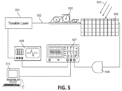
100811 FIG. 5 depicts an exemplary measurement setup that can be used to
process a set of
signals from an acousto-optic sensor device 505 that senses a set of
ultrasonic echoes 504 (also
24
CA 03174131 2022- 9- 29
WO 2021/202093
PCT/US2021/022412
referred to herein as the -ultrasonic signal"). The measurement setup can
include a single
wavelength light source, a broadband light source, or a tunable laser 501 that
propagates a set of
lights in an optical fiber 502, a fiber polarization controller 503 that can
be configured to control
the polarization of the light. The measurement setup can further include an
acousto-optic sensor
device 505 that can be configured to generate a first set of optical signals
based on propagation
of a first set of whispering gallery modes (WGMs) in a set of resonator nodes
(as described
above with respect to FIG. IA) included in the acousto-optic device 505. The
acousto-optic
sensor device 505 can be configured to receive a set of ultrasonic signals 504
and generate a
second set of optical signals based on propagating a second set of WGMs in set
of resonator
nodes. The acousto-optic sensor device 505 can be configured further to
transmit the first set of
optical signals and/or the second set of optical signals to the optical fiber
502. The measurement
setup can further include a photodetector (also referred to herein as "an
optical detector") 506
that receives the first set of optical signals and/or the second set of
optical signals and converts
them to a first set of electrical signals and/or a second set of electrical
signals. The photodetector
506 can be configured further to transmit the first set of electrical signals
and/or the second set
of electrical signals to an oscilloscope 507 operatively connected to a
computer device 510 to
process and analyze the first set of signals and/or the second set of signals.
The oscilloscope 507
can be configured further to transmit a set of analyzed signals to a function
generator 508. The
function generator can be configured to generate and transmit a set of
generation signals to the
broadband light source or the tunable laser 501 to control propagation of
light in the optical fiber
502
100821 In another exemplary measurement setup, the function generator 508 in
FIG.5 could be
replaced by a locking system, such as a Pound¨Drever¨Hall (PDH) locking
system, to set the
wavelength of the light source on the resonance slope of the WGM. The
photodetector 506 will
receive oscillating optical signals in response to a set of ultrasonic echoes.
100831 FIG. 6 depicts an exemplary measurement setup that can be used to
process a set of
signals from an acousto-optic sensor device 604 that senses a set of
ultrasonic echoes. The
measurement setup can include a laser 601 such as, for example, an optical
frequency comb
(OFC) laser source generated using either a digital modulating method or using
a Kerr four-
wave mixing (FWM) method, or any other laser suitable for the operation
frequency band of the
acousto-optic sensor device 604, to generate a laser light. The measurement
setup can further
CA 03174131 2022- 9- 29
WO 2021/202093
PCT/US2021/022412
include a beamsplitter 602 such as, for example, a 50:50 beamsplitter, an
80:20 beamsplitter, or
any other beamsplitters suitable for the measurement setup. The beam splitter
can be configured
to split the laser light to a first laser light and a second laser light. The
measurement setup can be
configured to direct the first laser light to an electro-optical modulator 603
to generate and
transmit a modulated laser light The measurement setup can be configured
further to direct the
modulated laser light to the acousto-optic sensor device 604 to generate a
first set of signals
corresponding to a first set of whispering gallery modes (WGMs). The acousto-
optic sensor
device 604 can be configured to receive a set of ultrasound signals and
generate a second set of
signals corresponding to a second set of WGMs. The measurement setup can be
configured
further to direct the first set of signals, the second set of signals, and/or
the second laser light to a
coherent receiver 605 to mix the second laser light with the first set of
signals and/or the second
set of signals and generate an electronic frequency signal. The measurement
setup can be
configured to transmit the electronic frequency signal to a Fast Fourier
Transformation (FFT)
module 606 operatively connected to a compute device to process and analyze a
difference
between the first set of signals and the second set of signals. In one
example, the OFC laser can
generate a set of comb beams, and each comb beam from the set of comb beams
can generate a
data point to detect the difference between the first set of signals and the
second set of signals. In
this example one set of comb beams can generate a set of data points
corresponding to the set of
comb beams. In some embodiments, use of an OFC laser source can advantageously
reduce
sensing time from milliseconds to a sensing time on the order of microseconds.
100841 Although in the examples above the optical microresonator array has
been used for
ultrasound detection, in some embodiments, the optical microresonator array
may be used for
nanoparticle detection, biomolecule detection, and/or the like In some
instances, by exposing
the set of resonator nodes to nanoparticles and/or biomolecules, the
environment surrounding the
resonator nodes at intersection of the set of optical fibers and the set of
optical waveguides can
change. The change of the environment can result in change of propagating
whispering gallery
modes (WGMs) at the set of resonator nodes and generate a second WGMs. A
change between a
first set of optical signals associated the first WGMs and a second set of
optical signals
associated with the second WGMs may be detected by a photodetector and/or an
optical
spectrum analyzer.
26
CA 03174131 2022- 9- 29
WO 2021/202093
PCT/US2021/022412
[0085] In some embodiments, an optical microresonator array such as those
described herein
may be included in an ultrasound probe (also referred to herein as "ultrasound
system"). The
ultrasound probe can include at least one optical waveguide to propagate a
light. The ultrasound
probe can further include multiple piezoelectric elements to generate a set of
ultrasound signals.
The ultrasound probe can further include multiple piezoelectric elements to
receive a set of
ultrasound echoes corresponding to the set of ultrasound signals. The
ultrasound probe can
further include a set of resonator nodes in a polymer structure. Each
resonator node having a
preassigned sensing location at an intersection of an optical waveguide and an
optical fiber. Each
resonator node configured to receive multiple ultrasound echoes and propagate
a set of
whispering gallery modes (WGMs). The set of optical fibers are coupled to the
set of optical
waveguides at the set of resonator nodes such that the set of optical fibers
are configured to
communicate to the set of optical waveguides a first set of signals
corresponding to the first set
of WGMs.
[0086] For example, FIG. 7 is a schematic description of an ultrasound probe,
utilizing optical
microresonator arrays such as those described herein. FIG. 8 is a cross-
sectional view of the
probe depicted in FIG. 7. The ultrasound probe can include an optical
microresonator array 801,
a matching layer 802, a piezoelectric crystal array 803, an electrical
connection array 804, a set
of optical fibers 805, a backing material 806, an acoustic insulator 807, and
a cable 808
connected to an ultrasound data acquisition. The ultrasound probe can be
coupled to a control
system, and a display, to perform an operation procedure as described in
further detail herein.
The backing material can include a damping material bonded to the back of the
package of the
probe to eliminate residual vibrations of operation environment, to improve
portability, and to
minimize echoes generated within the sensor structure
[0087] The ultrasound probe can be configured to propagate light from a light
source to the set
of optical microresonator array 801 to generate a first set of optical signals
corresponding to a
first set of WGMs propagating in each optical fiber at a resonator node of the
optical
microresonator array 801. The piezoelectric crystal array 803 can be
configured to receive an
electrical signal from the control system via the cable 808 and the electrical
connection array
804 to generate a set of ultrasound signals towards an object such that a set
of reflected
ultrasound echoes are generated in a direction toward the ultrasound probe.
The ultrasound
probe can be configured further to generate a second set of optical signals
corresponding to a
27
CA 03174131 2022- 9- 29
WO 2021/202093
PCT/US2021/022412
second set of WGMs in the optical microresonator array 801, after receiving
the set of
ultrasound echoes. The ultrasound probe can be optionally configured to
receive the set of
ultrasound echoes to generate a set of electrical signals. The ultrasound
probe can be configured
further to transmit the first set of signals and/or the second set of signals
via the set of optical
fibers 805, and/or optionally transmit a set of electrical signals via the
electrical connection array
804 to the cable 808 connected to the ultrasound data acquisition, the control
system, or the
display.
100881 In some embodiments, the ultrasound probe can be configured to repeat
the operation
procedure while scanning across a field of view by using a phased array of the
piezoelectric
crystal array. Doing so, will yield a line-by-line image using the
piezoelectric crystal array and
one low-resolution image in a lateral direction, for each resonator node.
Known Synthetic
Aperture (SA) algorithms can then be used to generate a high-resolution
optical microresonator
array sensor image.
100891 Furthermore, in some embodiments, one or more of the piezoelectric
elements can be
configured to receive ultrasound echoes corresponding to the set of
transmitted ultrasound
signals, and generate sensor signals based on these received ultrasound
echoes. For example, the
sensor signals generated by the piezoelectric elements may supplement or be
combined with the
signals communicated by the resonator nodes in any suitable manner (e.g., to
provide a multi-
modal sensor image).
100901 Additionally or alternatively, in some embodiments, the ultrasound
probe can be
configured to use different patterns of excitation such as, for example, using
a piezoelectric
crystal element or a group of piezoelectric crystals to transmit the
ultrasound signal, while using
all piezoelectric crystal elements in the piezoelectric crystal array to
receive the set of ultrasound
echoes, also known as Compressed Sensing (CS) method The general approach of
CS method is
to form a linear model that represents the process of signal acquisition from
an image (also
known as a forward model) and to solve the linear equation to get the image.
100911 The foregoing description, for purposes of explanation, used specific
nomenclature to
provide a thorough understanding of the invention. However, it will be
apparent to one skilled
in the art that specific details are not required in order to practice the
invention. Thus, the
foregoing descriptions of specific embodiments of the invention are presented
for purposes of
28
CA 03174131 2022- 9- 29
WO 2021/202093
PCT/US2021/022412
illustration and description. They are not intended to be exhaustive or to
limit the invention to
the precise forms disclosed; obviously, many modifications and variations are
possible in view
of the above teachings. The embodiments were chosen and described in order to
explain the
principles of the invention and its practical applications, they thereby
enable others skilled in the
art to utilize the invention and various embodiments with various
modifications as are suited to
the particular use contemplated. It is intended that the following claims and
their equivalents
define the scope of the invention.
29
CA 03174131 2022- 9- 29