Note: Descriptions are shown in the official language in which they were submitted.
METHOD AND APPARATUS FOR TRANSMITTING RANDOM
ACCESS SIGNAL
TECHNICAL FIELD
[0001] This application relates to the communications field, and
more specifically, to a
method and an apparatus for transmitting a random access signal.
BACKGROUND
[0002] In a conventional solution, a terminal may access a network
device by using a
two-step random access type or a four-step random access type. A random access
signal used for
random access may be generated by using a random access formula. The random
access signal
may be a message 1 in the four-step random access type, or may be a message A
in the two-step
random access type.
[0003] In addition, there is a variable subcarrier quantity
parameter in the random access
formula, and the subcarrier quantity parameter is used to indicate a frequency
domain interval
(which may also be referred to as a "guard interval") between a random access
signal and a data
signal. Therefore, to ensure accuracy of a generated random access signal to
improve random
access efficiency, how to determine the subcarrier quantity parameter needs to
be resolved
urgently.
SUMMARY
[0004] This application provides a method and an apparatus for
transmitting a random access
signal, to obtain an accurate subcarrier quantity parameter, thereby improving
random access
efficiency.
[0005] According to a first aspect, a method for transmitting a
random access signal is
provided. The method includes: receiving configuration information, where the
configuration
information is used to indicate a random access preamble length, a random
access signal
CA 03174302 2022- 9- 29 1
subcarrier spacing, and a data subcarrier spacing; determining a subcarrier
quantity parameter
based on at least one of the random access preamble length, the random access
signal subcarrier
spacing, and the data subcarrier spacing, where the subcarrier quantity
parameter includes a first
subcarrier quantity used to indicate a frequency resource start location of a
random access
preamble and a frequency resource start location of a physical random access
channel, and/or a
second subcarrier quantity used to indicate a frequency resource end location
of the random
access preamble and a frequency resource end location of the physical random
access channel;
generating a random access signal based on the subcarrier quantity parameter;
and sending the
random access signal.
[0006] A terminal receives the configuration information, and determines
the subcarrier
quantity parameter with reference to at least one of the random access
preamble length, the
random access signal subcarrier spacing, and the data subcarrier spacing that
are indicated by the
configuration information. In this way, the terminal can generate an accurate
random access
signal, thereby improving random access efficiency.
[0007] In some possible implementations, a value of the random access
signal subcarrier
spacing is any one of 120 kHz, 240 kHz, 480 kHz, 960 kHz, 1920 kHz, and 3840
kHz.
[0008] Embodiments of this application may be applied to a
scenario less than 52.6 GHz.
The subcarrier spacing may alternatively be greater than or equal to 240 kHz,
that is, this
application may also be applied to a scenario greater than or equal to 52.6
GHz, thereby
extending an application range of random access.
[0009] In some possible implementations, a value of the data
subcarrier spacing is any one of
240 kHz, 480 kHz, 960 kHz, 1920 kHz, and 3840 kHz.
[0010] This application may be applied to a scenario greater than
or equal to 52.6 GHz, to
implement random access, thereby extending an application range of random
access.
[0011] In some possible implementations, a value of the subcarrier quantity
parameter is any
one of-15, ¨7, ¨5, ¨3,¨i, 0, 1, 2, 3, 19, 23, 83, and 107.
[0012] Different values of the subcarrier quantity parameter may
flexibly adjust the first
subcarrier quantity and the second subcarrier quantity, that is, in
embodiments of this application,
sizes of guard intervals may be flexibly adjusted, to implement applicability
to different
scenarios.
[0013] In some possible implementations, the determining a
subcarrier quantity parameter
CA 03174302 2022- 9- 29
2
based on at least one of the random access preamble length, the random access
signal subcarrier
spacing, and the data subcarrier spacing includes: determining a total
subcarrier quantity
frequency domain width based on the random access preamble length, the random
access signal
subcarrier spacing, and the data subcarrier spacing; and determining the
subcarrier quantity
parameter based on the total subcarrier quantity frequency domain width, the
random access
signal subcarrier spacing, and the data subcarrier spacing.
[0014] The terminal may first determine the total subcarrier
quantity frequency domain
width, and then further determine the subcarrier quantity parameter, that is,
may indirectly obtain
the subcarrier quantity parameter. Therefore, embodiments of this application
provide an
implementation of determining a subcarrier quantity parameter, to help
generate an accurate
random access signal, and further help improve random access efficiency.
[0015] In some possible implementations, the determining a
subcarrier quantity parameter
based on at least one of the random access preamble length, the random access
signal subcarrier
spacing, and the data subcarrier spacing includes: determining the subcarrier
quantity parameter
in the second target parameter based on the random access signal subcarrier
spacing and the data
subcarrier spacing in the first target parameter.
[0016] The terminal may determine the subcarrier quantity
parameter with reference to the
random access signal subcarrier spacing and the data subcarrier spacing. For
example, the
terminal may store a mapping relationship of the random access signal
subcarrier spacing and the
data subcarrier spacing with the subcarrier quantity parameter. Therefore,
embodiments of this
application provide another implementation of determining a subcarrier
quantity parameter, to
help generate an accurate random access signal, and further help improve
random access
efficiency.
[0017] In some possible implementations, the first subcarrier
quantity and the second
subcarrier quantity are the same.
[0018] A guard interval 1 and a guard interval 2 may be the same,
so that the terminal may
implement same impact on data demodulation at two ends of the random access
signal, thereby
reducing complexity of the terminal.
[0019] In some possible implementations, the determining the
subcarrier quantity parameter
based on the total subcarrier quantity frequency domain width, the random
access signal
subcarrier spacing, and the data subcarrier spacing includes:
CA 03174302 2022- 9- 29
3
the subcarrier quantity parameter k conforms to:
Af
(GP ¨ )
k¨ = 2 2 + 0.5 '
AfRA
where GP represents the total subcarrier quantity frequency domain width, Af
represents the data subcarrier spacing, ALA represents the random access
signal subcarrier
spacing, and k represents the subcarrier quantity parameter.
[0020] The terminal or a network device may determine k by using
the foregoing formula,
to adjust the guard interval 1 and the guard interval 2 to be the same, so
that same impact is
implemented on data demodulation at two ends of the random access signal,
thereby reducing
complexity of the terminal.
[0021] In some possible implementations, LRA , Af , AfRA , and k meet at
least one of the
following correspondences:
LRA AfRA Af k
139 240 240 2
139 480 480 2
139 960 960 2
139 1920 1920 2
139 3840 3840 2
571 240 240 2
571 960 960 2
571 1920 1920 2
571 3840 3840 2
1151 480 480 0
1151 960 960 0
1151 1920 1920 0
1151 3840 3840 0
CA 03174302 2022- 9- 29
4
where Af represents the data subcarrier spacing, ALA represents the random
access signal subcarrier spacing, k represents the subcarrier quantity
parameter, and LRA
represents the random access preamble length.
[0022] The terminal or the network device may determine k by using
the foregoing table,
to adjust the guard interval 1 and the guard interval 2 to be the same, so
that same impact is
implemented on data demodulation at two ends of the random access signal,
thereby reducing
complexity of the terminal.
[0023] In some possible implementations, LRA , Af , AfRA , and k
meet at least one of the
following correspondences:
LRA AfR A Af k
139 120 240 2
139 120 480 1
139 240 480 2
139 120 960 23
139 240 960 1
139 480 960 2
139 120 1920 19
139 240 1920 23
139 480 1920 1
139 960 1920 2
139 120 3840 107
139 240 3840 19
139 480 3840 23
139 960 3840 1
139 1920 3840 2
571 120 240 2
571 120 480 1
571 240 480 2
CA 03174302 2022- 9- 29
5
LRA AfRA Af k
571 120 960 -1
571 240 960 1
571 480 960 2
571 120 1920 -5
571 240 1920 -1
571 480 1920 1
571 960 1920 2
571 120 3840 83
571 240 3840 -5
571 480 3840 -1
571 960 3840 1
571 1920 3840 2
1151 120 240 0
1151 120 480 -1
1151 240 480 0
1151 120 960 -3
1151 240 960 -1
1151 480 960 0
1151 120 1920 -7
1151 240 1920 -3
1151 480 1920 -1
1151 960 1920 0
1151 120 3840 -15
1151 240 3840 -7
1151 480 3840 -3
1151 960 3840 -1
1151 1920 3840 0
CA 03174302 2022- 9- 29
6
where Af represents the data subcarrier spacing, AL, represents the random
access signal subcarrier spacing, k represents the subcarrier quantity
parameter, and LRA
represents the random access preamble length.
[0024] The terminal or the network device may determine k by using
the foregoing table,
to adjust the guard interval 1 and the guard interval 2 to be the same, so
that same impact is
implemented on data demodulation at two ends of the random access signal,
thereby reducing
complexity of the terminal.
[0025] In some possible implementations, the first subcarrier
quantity and the total subcarrier
quantity frequency domain width are the same, and the second subcarrier
quantity is zero.
[0026] The guard intervals of the random access signal may be set to a
maximum at one end
and zero at the other end. For example, the guard interval 1 is a maximum, and
the guard interval
2 is zero. In this way, impact on other frequency division data may be
minimized by the guard
interval 1, thereby improving data demodulation performance. In addition, for
the guard interval
2, the network device may reduce interference by performing scheduling to
avoid data
transmission or scheduling low MCS data.
[0027] In some possible implementations, the determining the
subcarrier quantity parameter
in the target second parameter based on the total subcarrier quantity
frequency domain width, the
random access signal subcarrier spacing, and the data subcarrier spacing
includes:
the subcarrier quantity parameter k conforms to:
(GP ¨ Af )
k = 2 + 0.5 ,
AfRA
where GP represents the total subcarrier quantity frequency domain width, Af
represents the data subcarrier spacing, AfR, represents the random access
signal subcarrier
spacing, and k represents the subcarrier quantity parameter.
[0028] The terminal or the network device may meet the foregoing
relationship by setting k,
so that the guard interval 1 is a maximum, and the guard interval 2 is zero.
In this way, impact on
other frequency division data is minimized by the guard interval 1, thereby
improving data
demodulation performance.
CA 03174302 2022- 9- 29
7
[0029] In some possible implementations, the determining the
subcarrier quantity parameter
in the target second parameter based on the total subcarrier quantity
frequency domain width, the
random access signal subcarrier spacing, and the data subcarrier spacing
includes:
the subcarrier quantity parameter k conforms to:
(GP + Af )
2
k = ___________________________ + 0.5 ,
AfRA
where GP represents the total subcarrier quantity frequency domain width, Af
represents the data subcarrier spacing, AL, represents the random access
signal subcarrier
spacing, and k represents the subcarrier quantity parameter.
[0030] The terminal or the network device may meet the foregoing
relationship by setting k,
so that the guard interval 1 is a maximum, and the guard interval 2 is zero.
In this way, impact on
other frequency division data is minimized by the guard interval 1, thereby
improving data
demodulation performance.
[0031] In some possible implementations, the first subcarrier
quantity is zero, and the second
subcarrier quantity and the total subcarrier quantity frequency domain width
are the same.
[0032] The guard intervals of the random access signal may be set to a
maximum at one end
and zero at the other end. For example, the guard interval 2 is a maximum, and
the guard interval
1 is zero. In this way, impact on other frequency division data may be
minimized by the guard
interval 2, thereby improving data demodulation performance. In addition, for
the guard interval
1, the network device may reduce interference by performing scheduling to
avoid data
transmission or scheduling low MCS data.
[0033] In some possible implementations, the determining the
subcarrier quantity parameter
based on the random access signal subcarrier spacing and the data subcarrier
spacing includes:
the subcarrier quantity parameter k conforms to:
(0 ¨ Af )
2
AfRA
where Af represents the data subcarrier spacing, AfR, represents the random
CA 03174302 2022- 9- 29
8
access signal subcarrier spacing, and k represents the subcarrier quantity
parameter.
[0034] The terminal or the network device may meet the foregoing
relationship by setting k,
so that the guard interval 2 is a maximum, and the guard interval 1 is zero.
In this way, impact on
other frequency division data is minimized by the guard interval 2, thereby
improving data
demodulation performance.
[0035] In some possible implementations, the determining the
subcarrier quantity parameter
based on the random access signal subcarrier spacing and the data subcarrier
spacing includes:
the subcarrier quantity parameter k conforms to:
f¨ A
k = 261RA+ 0.5,
where Af represents the data subcarrier spacing, AfRA represents the random
access signal subcarrier spacing, and k represents the subcarrier quantity
parameter.
[0036] The terminal or the network device may meet the foregoing
relationship by setting k,
so that the guard interval 2 is a maximum, and the guard interval 1 is zero.
In this way, impact on
other frequency division data is minimized by the guard interval 2, thereby
improving data
demodulation performance.
[0037] According to a second aspect, a method for transmitting a
random access signal is
provided. The method includes: receiving configuration information, where the
configuration
information is used to indicate a random access preamble length, a random
access signal
subcarrier spacing, and a data subcarrier spacing, at least one of the random
access preamble
length, the random access signal subcarrier spacing, and the data subcarrier
spacing is used to
determine a subcarrier quantity parameter, the subcarrier quantity parameter
is used to generate a
random access signal, and the subcarrier quantity parameter includes a first
subcarrier quantity
used to indicate a frequency resource start location of a random access
preamble and a frequency
resource start location of a physical random access channel, and/or a second
subcarrier quantity
used to indicate a frequency resource end location of the random access
preamble and a
frequency resource end location of the physical random access channel; and
sending the random
access signal.
[0038] A terminal receives the configuration information, and
determines the subcarrier
CA 03174302 2022- 9- 29
9
quantity parameter with reference to at least one of the random access
preamble length, the
random access signal subcarrier spacing, and the data subcarrier spacing that
are indicated by the
configuration information. In this way, the terminal can generate an accurate
random access
signal, thereby improving random access efficiency.
[0039] In some possible implementations, a value of the random access
signal subcarrier
spacing is any one of 120 kHz, 240 kHz, 480 kHz, 960 kHz, 1920 kHz, and 3840
kHz.
[0040] In some possible implementations, a value of the data
subcarrier spacing is any one of
240 kHz, 480 kHz, 960 kHz, 1920 kHz, and 3840 kHz.
[0041] In some possible implementations, a value of the subcarrier
quantity parameter is any
one of ¨15, ¨7, ¨5, ¨3, ¨1, 0, 1, 2, 3, 19, 23, 83, and 107.
[0042] In some possible implementations, the first subcarrier
quantity and the second
subcarrier quantity are the same.
[0043] In some possible implementations, the random access signal
subcarrier spacing, the
data subcarrier spacing, and the subcarrier quantity parameter meet the
following relationship:
1 ¨Af
5 (GP __ )
2 2 0.5, and
k¨ =
Af RA
GP = ceil(LRA* Af RA I (Af * N))* (Af * N)¨ LRA* Af RA ,
where Af represents the data subcarrier spacing, AfRA represents the random
access signal subcarrier spacing, k represents the subcarrier quantity
parameter, and L RA
represents the random access preamble length.
[0044] In some possible implementations, the first subcarrier quantity and
the total subcarrier
quantity frequency domain width are the same, and the second subcarrier
quantity is zero.
[0045] In some possible implementations, the determining the
subcarrier quantity parameter
in the target second parameter based on the total subcarrier quantity
frequency domain width, the
random access signal subcarrier spacing, and the data subcarrier spacing
includes:
the subcarrier quantity parameter k conforms to:
(GP ¨ Af)
k = 2 + 0.5 ,
AfRA
CA 03174302 2022- 9- 29
where GP represents the total subcarrier quantity frequency domain width, Af
represents the data subcarrier spacing, AfRA represents the random access
signal subcarrier
spacing, and k represents the subcarrier quantity parameter.
[0046] In some possible implementations, the first subcarrier
quantity is zero, and the second
subcarrier quantity and the total subcarrier quantity frequency domain width
are the same.
[0047] In some possible implementations, the random access signal
subcarrier spacing, the
data subcarrier spacing, and the subcarrier quantity parameter meet the
following relationship:
(0 ¨ Af )
2
k = _________________________ + 0.5 ,
AfRA
where Af represents the data subcarrier spacing, ALA represents the random
access signal subcarrier spacing, and k represents the subcarrier quantity
parameter.
[0048] According to a third aspect, a method for transmitting a
random access signal is
provided. The method includes: sending configuration information, where the
configuration
information is used to indicate a random access preamble length, a random
access signal
subcarrier spacing, and a data subcarrier spacing; and receiving a random
access signal, where
the random access signal is generated based on a subcarrier quantity
parameter, the subcarrier
quantity parameter is determined by at least one of the random access preamble
length, the
random access signal subcarrier spacing, and the data subcarrier spacing, and
the subcarrier
quantity parameter includes a first subcarrier quantity used to indicate a
frequency resource start
location of a random access preamble and a frequency resource start location
of a physical
random access channel, and/or a second subcarrier quantity used to indicate a
frequency resource
end location of the random access preamble and a frequency resource end
location of the
physical random access channel.
[0049] A network device sends, to a terminal, the configuration
information used to indicate
the random access preamble length, the random access signal subcarrier
spacing, and the data
subcarrier spacing, so that the terminal may determine the subcarrier quantity
parameter with
reference to at least one of the random access preamble length, the random
access signal
subcarrier spacing, and the data subcarrier spacing. That is, the
configuration information sent by
the network device can enable the terminal to generate an accurate random
access signal, thereby
CA 03174302 2022- 9- 29
11
improving random access efficiency.
[0050] In some possible implementations, a value of the random
access signal subcarrier
spacing is any one of 120 kHz, 240 kHz, 480 kHz, 960 kHz, 1920 kHz, and 3840
kHz.
[0051] In some possible implementations, a value of the data
subcarrier spacing is any one of
240 kHz, 480 kHz, 960 kHz, 1920 kHz, and 3840 kHz.
[0052] In some possible implementations, a value of the subcarrier
quantity parameter is any
one of-15, ¨7, ¨5, ¨3,¨i, 0, 1, 2, 3, 19, 23, 83, and 107.
[0053] In some possible implementations, the first subcarrier
quantity and the second
subcarrier quantity are the same.
[0054] In some possible implementations, the random access signal
subcarrier spacing, the
data subcarrier spacing, and the subcarrier quantity parameter meet the
following relationship:
(GP Af )
k¨ = 2 2 0.5 , and
AfRA
GP = ceil(LRA* Af RA I (Af * N)) * (Af * N) ¨ LRA * AfRA ,
where Af represents the data subcarrier spacing, AfRA represents the random
access signal subcarrier spacing, and k represents the subcarrier quantity
parameter.
[0055] In some possible implementations, the first subcarrier
quantity and the total subcarrier
quantity frequency domain width are the same, and the second subcarrier
quantity is zero.
[0056] In some possible implementations, the random access signal
subcarrier spacing, the
data subcarrier spacing, and the subcarrier quantity parameter meet the
following relationship:
(GP ¨ Af )
AfRA
GP = ceil(LRA* Af RA I (Af * N)) * (Af * N) ¨ LRA * AfRA ,
where Af represents the data subcarrier spacing, AfRA represents the random
access signal subcarrier spacing, and k represents the subcarrier quantity
parameter.
[0057] In some possible implementations, the random access signal
subcarrier spacing, the
data subcarrier spacing, and the subcarrier quantity parameter meet the
following relationship:
CA 03174302 2022- 9- 29
12
(GP + Af)
2
k = ___________________________ 0.5 , and
AfRA
GP = ceil(LRA* AfRA I (Af * N))* (Af * N)¨ LRA* Af RA ,
where Af represents the data subcarrier spacing, ALA represents the random
access signal subcarrier spacing, and k represents the subcarrier quantity
parameter.
[0058] In some possible implementations, the first subcarrier quantity is
zero, and the second
subcarrier quantity and the total subcarrier quantity frequency domain width
are the same.
[0059] In some possible implementations, the random access signal
subcarrier spacing, the
data subcarrier spacing, and the subcarrier quantity parameter meet the
following relationship:
(0 ¨ Af )
2
k = + 0.5 ,
AfRA
where Af represents the data subcarrier spacing, AfRA represents the random
access signal subcarrier spacing, and k represents the subcarrier quantity
parameter.
[0060] In some possible implementations, the random access signal
subcarrier spacing, the
data subcarrier spacing, and the subcarrier quantity parameter meet the
following relationship:
__________________________ +0.5 ,
2AfRA
where Af represents the data subcarrier spacing, AfRA represents the random
access signal subcarrier spacing, and k represents the subcarrier quantity
parameter.
[0061] According to a fourth aspect, an apparatus for
transmitting a random access signal is
provided. The apparatus may be a terminal, or may be a chip in the terminal.
The apparatus has
functions of implementing the first aspect and the possible implementations.
The functions may
be implemented by hardware, or may be implemented by hardware executing
corresponding
software. The hardware or the software includes one or more modules
corresponding to the
functions.
[0062] In a possible design, the apparatus includes a transceiver
module and a processing
module. The transceiver module may include a receiving module and a sending
module. The
CA 03174302 2022- 9- 29
13
transceiver module may be, for example, at least one of a transceiver, a
receiver, or a transmitter.
The transceiver module may include a radio frequency circuit or an antenna.
The processing
module may be a processor. Optionally, the apparatus further includes a
storage module, and the
storage module may be, for example, a memory. When the storage module is
included, the
storage module is configured to store instructions. The processing module is
connected to the
storage module, and the processing module may execute the instructions stored
in the storage
module or instructions from elsewhere, to enable the apparatus to perform the
communications
method in the first aspect and the possible implementations. In this design,
the apparatus may be
a terminal.
[0063] In another possible design, when the apparatus is a chip, the chip
includes a
transceiver module and a processing module. The transceiver module may include
a receiving
module and a sending module. The transceiver module may be, for example, an
input/output
interface, a pin, or a circuit on the chip. The processing module may be, for
example, a processor.
The processing module may execute instructions, to enable the chip in the
terminal to perform
the communications method in the first aspect and any possible implementation.
Optionally, the
processing module may execute instructions in a storage module. The storage
module may be a
storage module, for example, a register or a cache, in the chip.
Alternatively, the storage module
may be located in the communications device but located outside the chip, for
example, a
read-only memory (read-only memory, ROM) or another type of static storage
device that can
store static information and instructions, or a random access memory (random
access memory,
RAM).
[0064] Any processor mentioned above may be a general-purpose
central processing unit
(CPU), a microprocessor, an application-specific integrated circuit
(application-specific
integrated circuit, ASIC), or one or more integrated circuits configured to
control program
execution of the communications methods in the foregoing aspects.
[0065] According to a fifth aspect, an apparatus for transmitting
a random access signal is
provided. The apparatus may be a terminal, or may be a chip in the terminal.
The apparatus has
functions of implementing the second aspect and the possible implementations.
The functions
may be implemented by hardware, or may be implemented by hardware executing
corresponding
software. The hardware or the software includes one or more modules
corresponding to the
functions.
CA 03174302 2022- 9- 29
14
[0066] In a possible design, the apparatus includes a transceiver
module. Optionally, the
apparatus further includes a processing module. The transceiver module may
include a receiving
module and a sending module. The transceiver module may be, for example, at
least one of a
transceiver, a receiver, or a transmitter. The transceiver module may include
a radio frequency
circuit or an antenna. The processing module may be a processor.
[0067] Optionally, the apparatus further includes a storage
module, and the storage module
may be, for example, a memory. When the storage module is included, the
storage module is
configured to store instructions. The processing module is connected to the
storage module, and
the processing module may execute the instructions stored in the storage
module or instructions
from elsewhere, to enable the apparatus to perform the communications method
in the second
aspect and the possible implementations. In this design, the apparatus may be
a terminal.
[0068] In another possible design, when the apparatus is a chip,
the chip includes a
transceiver module. Optionally, the chip further includes a processing module.
The transceiver
module may include a receiving module and a sending module. The transceiver
module may be,
for example, an input/output interface, a pin, or a circuit on the chip. The
processing module may
be, for example, a processor. The processing module may execute instructions,
to enable the chip
in the terminal to perform the communications method in the second aspect and
any possible
implementation.
[0069] Optionally, the processing module may execute instructions
in a storage module. The
storage module may be a storage module, for example, a register or a cache, in
the chip.
Alternatively, the storage module may be located in the communications device
but located
outside the chip, for example, a read-only memory (read-only memory, ROM) or
another type of
static storage device that can store static information and instructions, or a
random access
memory (random access memory, RAM).
[0070] Any processor mentioned above may be a general-purpose central
processing unit
(CPU), a microprocessor, an application-specific integrated circuit
(application-specific
integrated circuit, ASIC), or one or more integrated circuits configured to
control program
execution of the communications methods in the foregoing aspects.
[0071] According to a sixth aspect, an apparatus for transmitting
a random access signal is
provided. The apparatus may be a network device, or may be a chip in the
network device. The
apparatus has functions of implementing the third aspect and the possible
implementations. The
CA 03174302 2022- 9- 29
functions may be implemented by hardware, or may be implemented by hardware
executing
corresponding software. The hardware or the software includes one or more
modules
corresponding to the functions.
[0072] In a possible design, the apparatus includes a transceiver
module. Optionally, the
apparatus may further include a processing module. The transceiver module may
include a
receiving module and a sending module. The transceiver module may be, for
example, at least
one of a transceiver, a receiver, or a transmitter. The transceiver module may
include a radio
frequency circuit or an antenna. The processing module may be a processor.
[0073] Optionally, the apparatus further includes a storage
module, and the storage module
may be, for example, a memory. When the storage module is included, the
storage module is
configured to store instructions. The processing module is connected to the
storage module, and
the processing module may execute the instructions stored in the storage
module or instructions
from elsewhere, to enable the apparatus to perform the method in the third
aspect or any possible
implementation of the third aspect. In this design, the apparatus may be a
network device.
[0074] In another possible design, when the apparatus is a chip, the chip
includes a
transceiver module. Optionally, the apparatus may further include a processing
module. The
transceiver module may include a receiving module and a sending module. The
transceiver
module may be, for example, an input/output interface, a pin, or a circuit on
the chip. The
processing module may be, for example, a processor. The processing module may
execute
instructions, to enable the chip in the network device to perform the
communications method in
the third aspect and any possible implementation.
[0075] Optionally, the processing module may execute instructions
in a storage module. The
storage module may be a storage module, for example, a register or a cache, in
the chip.
Alternatively, the storage module may be located in the communications device
but located
outside the chip, for example, a ROM or another type of static storage device
that can store static
information and instructions, or a RAM.
[0076] Any processor mentioned above may be a CPU, a
microprocessor, an
application-specific integrated circuit ASIC, or one or more integrated
circuits configured to
control program execution of the communications methods in the foregoing
aspects.
[0077] According to a seventh aspect, a computer storage medium is
provided. The computer
storage medium stores program code, and the program code is used to indicate
instructions for
CA 03174302 2022- 9- 29
16
performing the method in the first aspect or the second aspect, and any
possible implementation
of the first aspect or the second aspect.
[0078] According to an eighth aspect, a computer storage medium is
provided. The computer
storage medium stores program code, and the program code is used to indicate
instructions for
performing the method in the third aspect and any possible implementation of
the third aspect.
[0079] According to a ninth aspect, a computer program product
including instructions is
provided. When the computer program product runs on a computer, the computer
is enabled to
perform the method in the first aspect or the second aspect, or any possible
implementation of
the first aspect or the second aspect.
[0080] According to a tenth aspect, a computer program product including
instructions is
provided. When the computer program product runs on a computer, the computer
is enabled to
perform the method in the third aspect or any possible implementation of the
third aspect.
[0081] According to an eleventh aspect, a communications system is
provided. The
communications system includes the apparatus according to the fourth aspect
and the apparatus
according to the sixth aspect.
[0082] According to a twelfth aspect, a communications system is
provided. The
communications system includes the apparatus according to the fifth aspect and
the apparatus
according to the sixth aspect.
[0083] Based on the foregoing technical solutions, the terminal
receives the configuration
information, and determines the subcarrier quantity parameter with reference
to at least one of
the random access preamble length, the random access signal subcarrier
spacing, and the data
subcarrier spacing that are indicated by the configuration information. In
this way, the terminal
can generate an accurate random access signal, thereby improving random access
efficiency.
BRIEF DESCRIPTION OF DRAWINGS
[0084] FIG 1 is a schematic diagram of a communications system according to
this
application;
[0085] FIG 2 is a schematic flowchart of a random access method in
a conventional solution;
[0086] FIG 3 is a schematic flowchart of another random access
method in a conventional
solution;
CA 03174302 2022- 9- 29
17
[0087] FIG 4 is a schematic diagram of a frequency domain resource
structure according to
an embodiment of this application;
[0088] FIG 5 is a schematic diagram of a frequency domain resource
structure according to
another embodiment of this application;
[0089] FIG 6 is a schematic flowchart of a method for transmitting a random
access signal
according to an embodiment of this application;
[0090] FIG 7 is a schematic diagram of a frequency domain resource
structure according to
an embodiment of this application;
[0091] FIG 8 is a schematic block diagram of an apparatus for
transmitting a random access
signal according to an embodiment of this application;
[0092] FIG 9 is a schematic diagram of a structure of an apparatus
for transmitting a random
access signal according to an embodiment of this application;
[0093] FIG 10 is a schematic block diagram of an apparatus for
transmitting a random
access signal according to another embodiment of this application;
[0094] FIG 11 is a schematic diagram of a structure of an apparatus for
transmitting a
random access signal according to another embodiment of this application;
[0095] FIG 12 is a schematic diagram of an apparatus for
transmitting a random access
signal according to another specific embodiment of this application;
[0096] FIG 13 is a schematic diagram of an apparatus for
transmitting a random access
signal according to another specific embodiment of this application;
[0097] FIG 14 is a schematic diagram of an apparatus for
transmitting a random access
signal according to another specific embodiment of this application; and
[0098] FIG 15 is a schematic diagram of an apparatus for
transmitting a random access
signal according to another specific embodiment of this application.
DESCRIPTION OF EMBODIMENTS
[0099] The following describes technical solutions of this
application with reference to the
accompanying drawings.
[00100] The technical solutions in embodiments of this application may be
applied to various
communications system, for example, a global system for mobile communications
(global
CA 03174302 2022- 9- 29
18
system for mobile communications, GSM) system, a code division multiple access
(code
division multiple access, CDMA) system, a wideband code division multiple
access (wideband
code division multiple access, WCDMA) system, a general packet radio service
(general packet
radio service, GPRS), a long term evolution (long term evolution, LTE) system,
an LTE
frequency division duplex (frequency division duplex, FDD) system, an LTE time
division
duplex (time division duplex, TDD) system, a universal mobile
telecommunication system
(universal mobile telecommunication system, UMTS), a worldwide
interoperability for
microwave access (worldwide interoperability for microwave access, WiMAX)
communications
system, a future 5th generation (5th generation, 5G) system, or a new radio
(new radio, NR)
system.
[00101] A terminal in embodiments of this application may be user equipment,
an access
terminal, a subscriber unit, a subscriber station, a mobile station, a remote
station, a remote
terminal, a mobile device, a user terminal, a terminal device, a wireless
communications device,
a user agent, or a user apparatus. The terminal may alternatively be a
cellular phone, a cordless
phone, a session initiation protocol (session initiation protocol, SIP) phone,
a wireless local loop
(wireless local loop, WLL) station, a personal digital assistant (personal
digital assistant, PDA), a
handheld device having a wireless communications function, a computing device,
another
processing device connected to a wireless modem, a vehicle-mounted device, a
wearable device,
a terminal in a future 5G network, a terminal in a future evolved public land
mobile network
(public land mobile network, PLMN), or the like. This is not limited in
embodiments of this
application.
[00102] A network device in embodiments of this application may be a device
configured to
communicate with a terminal. The network device may be a base transceiver
station (base
transceiver station, BTS) in the global system for mobile communications
(global system for
mobile communications, GSM) system or the code division multiple access (code
division
multiple access, CDMA) system, or may be a NodeB (NodeB, NB) in the wideband
code
division multiple access (wideband code division multiple access, WCDMA)
system, or may be
an evolved NodeB (evolved NodeB, eNB or eNodeB) in the LTE system, or may be a
radio
controller in a cloud radio access network (Cloud radio access network, CRAN)
scenario, or the
network device may be a relay station, an access point, a vehicle-mounted
device, a wearable
device, a network device in a future 5G network, a network device in a future
evolved PLMN
CA 03174302 2022- 9- 29
19
network, or an antenna panel or an antenna panel group (including a plurality
of antenna panels)
of a base station in a 5G system, or may be a network node that constitutes a
5G base station
(gNB) or a transmission point, for example, a baseband unit (baseband unit,
BBU) or a
distributed unit (distributed unit, DU). This is not limited in embodiments of
this application.
[00103] In some deployment, the gNB may include a centralized unit
(centralized unit, CU)
and the DU. The gNB may further include an active antenna unit (active antenna
unit, AAU).
The CU implements some functions of the gNB, and the DU implements some
functions of the
gNB. For example, the CU is responsible for processing a non-real-time
protocol and service, to
implement functions of radio resource control (radio resource control, RRC)
and packet data
convergence protocol (packet data convergence protocol, PDCP) layers. The DU
is responsible
for processing a physical layer protocol and a real-time service, to implement
functions of a
radio link control (radio link control, RLC) layer, a media access control
(media access control,
MAC) layer, and a physical (physical, PHY) layer. The AAU implements some
physical layer
processing functions, radio frequency processing, and a function related to an
active antenna.
Information at the RRC layer eventually becomes information at the PHY layer,
or is converted
from the information at the PHY layer. Therefore, in the architecture, higher
layer signaling such
as RRC layer signaling may also be considered as being sent by the DU or sent
by the DU and
the AAU. It may be understood that the network device may be a device
including one or more
of a CU node, a DU node, and an AAU node. In addition, the CU may be
classified as a network
device in a radio access network (radio access network, RAN), or the CU may be
classified as a
network device in a core network (core network, CN). This is not limited in
this application.
[00104] In embodiments of this application, the terminal or the network device
includes a
hardware layer, an operating system layer running above the hardware layer,
and an application
layer running above the operating system layer. The hardware layer includes
hardware such as a
central processing unit (central processing unit, CPU), a memory management
unit (memory
management unit, MMU), and a memory (also referred to as a main memory). The
operating
system may be any one or more computer operating systems that implement
service processing
through a process (process), for example, a Linux operating system, a Unix
operating system, an
Android operating system, an iOS operating system, or a Windows operating
system. The
application layer includes applications such as a browser, an address book,
word processing
software, and instant messaging software. In addition, a specific structure of
an execution body
CA 03174302 2022- 9- 29
of a method provided in embodiments of this application is not particularly
limited in
embodiments of this application, provided that a program that records code of
the method
provided in embodiments of this application can be run to perform
communication according to
the method provided in embodiments of this application. For example, the
method provided in
embodiments of this application may be performed by the terminal or the
network device, or a
functional module that can invoke and execute the program in the terminal or
the network
device.
[00105] In addition, aspects or features of this application may be
implemented as a method,
an apparatus, or a product that uses standard programming and/or engineering
technologies. The
term "product" used in this application covers a computer program that can be
accessed from any
computer-readable component, carrier, or medium. For example, a computer-
readable medium
may include but is not limited to: a magnetic storage component (for example,
a hard disk, a
floppy disk, or a magnetic tape), an optical disc (for example, a compact disc
(compact disc, CD)
or a digital versatile disc (digital versatile disc, DVD)), a smart card and a
flash memory
component (for example, an erasable programmable read-only memory (erasable
programmable
read-only memory, EPROM), a card, a stick, or a key drive). In addition,
various storage media
described in this specification may indicate one or more devices and/or other
machine-readable
media that are configured to store information. The term "machine-readable
media" may include
but is not limited to a wireless channel, and various other media that can
store, include, and/or
carry instructions and/or data.
[00106] The following describes in detail terms in this application.
[00107] 1. Random access preamble:
[00108] The random access preamble may be actual content that is sent by a
terminal on a
physical random access channel. The random access preamble is a ZC sequence.
The ZC
sequence preamble may be generated by using different cyclic shifts. Different
ZC sequence
preambles may be used for different users. In LTE and 5G NR systems, a cell
usually has 64
different random access preambles.
[00109] 2. Antenna port:
[00110] The antenna port is a logical concept, and there is no direct
correspondence between
an antenna port and a physical antenna. The antenna port is usually associated
with a reference
signal, and may be specifically understood as a transceiver interface on a
channel through which
CA 03174302 2022- 9- 29
21
the reference signal passes. For a low frequency, one antenna port may
correspond to one or
more antenna array elements, and these array elements jointly send a reference
signal. A receive
end may consider received reference signals as a whole, without distinguishing
the array
elements from which the reference signals are sent. For a high frequency
system, a plurality of
antenna ports may correspond to one beam. Similarly, a receive end may only
need to consider
the beam as one interface, without distinguishing each array element.
[00111] 3. Licensed resource:
[00112] The licensed resource is usually a resource that can provide high
communications
quality, which is generally a time-frequency resource whose use needs to be
approved by a
national or local wireless committee. Different systems such as an LTE system
and a Wi-Fi
system, or systems of different operators cannot share a licensed time-
frequency resource.
[00113] 4. Unlicensed resource:
[00114] The unlicensed resource may offload traffic for a licensed resource to
obtain good
coverage and capacity, thereby improving user experience. Specifically, the
unlicensed resource
may be a resource that may be shared by a plurality of communications devices.
Sharing of the
unlicensed resource means that for use of a particular spectrum, limitations
are posed only on
indicators such as transmit power and out-of-band emission, to ensure that a
plurality of devices
sharing the band meet a basic coexistence requirement. An operator may
implement network
traffic offloading by using an unlicensed resource, but needs to obey
regulatory requirements of
different regions and different spectrums on the unlicensed resource. These
requirements are
usually posed to protect a public system such as radar and ensure that a
plurality of systems
fairly coexist and causes negative impact to each other as little as possible,
and include a transmit
power limit, an out-of-band emission specification, indoor and outdoor use
restrictions.
Moreover, some regions further have some additional coexistence policies and
the like. For
example, communications devices may use a time-frequency resource in a
contention manner or
a listening manner, for example, a manner specified in listen before talk
(listen before talk, LBT).
[00115] For example but not for limitation, in embodiments of the present
invention, the
unlicensed resource (specifically, an unlicensed resource) may include a band
close to 5 GHz, a
band close to 2.4 GHz, a band close to 3.5 GHz, and a band close to 6 GHz.
[00116] Moreover, for example but not for limitation, in embodiments of the
present invention,
a communications system may use, for example, a licensed-assisted access
(licensed-assisted
CA 03174302 2022- 9- 29
22
access, LAA) technology, a dual connectivity (dual connectivity, DC)
technology, or a
standalone (standalone) technology. LAA includes using a carrier aggregation
(carrier
aggregation, CA) configuration and structure in the existing LTE system, and
on the basis of
configuring a carrier (licensed carrier) in a licensed band of an operator for
communication,
configuring carriers (unlicensed carriers) on a plurality of unlicensed
resources and performing
communication by using an unlicensed carrier with assistance of the licensed
carrier. That is, an
LTE device may use, in a CA manner, the licensed carrier as a primary
component carrier
(primary component carrier, PCC) or a primary serving cell (primary cell,
PCell), and the
unlicensed carrier as a secondary component carrier (secondary component
carrier, SCC) or a
secondary serving cell (secondary cell, SCell). The dual connectivity DC
technology includes a
technology of jointly using a licensed carrier and an unlicensed carrier in a
non-CA manner, or
may further include a technology of jointly using a plurality of unlicensed
carriers in a non-CA
manner. The LTE device may alternatively be directly deployed on an unlicensed
carrier through
independent deployment.
[00117] It may be understood that, embodiments of this application may be
applied to a
licensed resource, and may also be applied to an unlicensed resource.
[00118] 5. Bandwidth (bandwidth):
[00119] The bandwidth may be understood as continuous or discontinuous
resources in
frequency domain. For example, the bandwidth may be a cell (cell), a carrier,
or a bandwidth part
(bandwidth part, BWP). The cell may be a serving cell of a terminal. The
serving cell is
described by a high layer from a perspective of a resource management,
mobility management,
or service unit. A coverage area of each network device may be divided into
one or more serving
cells, and the serving cell may be considered as including a specific
frequency domain resource,
that is, one serving cell may include one or more carriers. The concept of
carrier is described
from a perspective of signal generation at a physical layer. One carrier is
defined by one or more
frequencies, corresponds to continuous or discontinuous spectrums, and is
configured to carry
communications data between a network device and a terminal. A downlink
carrier may be
configured for downlink transmission, and an uplink carrier may be configured
for uplink
transmission. In addition, one carrier may include one or more bandwidth
parts.
[00120] It should be noted that if one cell includes one carrier, one carrier
may be considered
as an independent cell without considering a physical location. That is, the
carrier may be
CA 03174302 2022- 9- 29
23
replaced with the cell equivalently.
[00121] It should be understood that the BWP may be referred to as a carrier
bandwidth part
(carrier bandwidth part), a subband (subband) bandwidth, a narrowband
(narrowband) bandwidth,
or another name. For ease of description, the following embodiments use the
BWP as an
example for description, but this is not limited in this application.
[00122] It should be noted that with continuous development of technologies,
terms in
embodiments of this application may change, but all of them fall within the
protection scope of
this application.
[00123] FIG 1 is a schematic diagram of a communications system according to
this
application. The communications system in FIG 1 may include at least one
terminal (for
example, a terminal 10, a terminal 20, a terminal 30, a terminal 40, a
terminal 50, and a terminal
60) and a network device 70. The network device 70 is configured to provide a
communications
service for the terminal and access a core network. The terminal may access a
network by
searching for a synchronization signal, a broadcast signal, or the like sent
by the network device
70, to communicate with the network. The terminal 10, the terminal 20, the
terminal 30, the
terminal 40, and the terminal 60 in FIG 1 may perform uplink and downlink
transmission with
the network device 70. For example, the network device 70 may send downlink
signals to the
terminal 10, the terminal 20, the terminal 30, the terminal 40, and the
terminal 60, and may
receive uplink signals sent by the terminal 10, the terminal 20, the terminal
30, the terminal 40,
and the terminal 60.
[00124] In addition, the terminal 40, the terminal 50, and the terminal 60 may
also be
considered as a communications system. The terminal 60 may send downlink
signals to the
terminal 40 and the terminal 50, or may receive uplink signals sent by the
terminal 40 and the
terminal 50.
[00125] It should be noted that embodiments of this application may be applied
to a
communications system including one or more network devices, and may also be
applied to a
communications system including one or more terminals. This is not limited in
this application.
[00126] It should be understood that the communications system may include one
or more
network devices. One network device may send data or control signaling to one
or more
terminals. A plurality of network devices may simultaneously send data or
control signaling to
one or more terminals.
CA 03174302 2022- 9- 29
24
[00127] FIG 2 is a schematic diagram of a random access process of a four-step
random
access type in a conventional solution. After selecting a proper cell to
complete camping, a
terminal may initiate random access. As shown in FIG 4, TIE sends a message 1
(message 1, msg
1) to a network device. The message 1 is a random access preamble (preamble).
After detecting
the random access preamble, the network device returns a response message,
that is, a message 2
(message 2), to the TIE. The message 2 includes an uplink resource allocated
by the network
device to the TIE. After receiving the message 2, the TIE sends a message 3 on
the uplink
resource indicated by the message 2. If the network device can correctly
decode the message 3
(message 3), the network device returns a message 4 (message 4) to the TIE.
The message 4 is
used to notify the TIE of a success in contention. After the foregoing four
steps, a random access
procedure succeeds.
[00128] FIG 3 is a schematic diagram of a random access process of a two-step
random
access type in a conventional solution. In the two-step random access process,
TIE adds both a
random access preamble and data (preamble and data) to a message A. The data
part is used for
contention resolution, for example, a radio resource control (radio resource
control, RRC)
message. If there is no conflict between UEs, a network device returns a
message B to the UE
after successfully decoding the message 1. The message B includes both a
response to the
random access preamble and a response to the data. The response to the random
access preamble
is a random access response (random access response, RAR). The response to the
data is usually
an RRC message. The two responses may be sent simultaneously or sequentially.
The TIE may
independently decode the two responses. After receiving the message 2, the TIE
learns that
random access succeeds.
[00129] It may be understood that, if there is a conflict between UEs, the
network device may
not successfully decode the data in the message A. In this case, the network
device does not send
the message 2 to the TIE. After sending the message 1, the TIE waits for a
time window. If the TIE
does not receive the message 2, the TIE considers that random access fails.
[00130] In a conventional solution, a terminal may generate, based on a random
access
formula, a random access signal used for random access. For example, the
random access
formula is as follows:
S" (t) = ELRA (p RA) it k=ciak e (1)
CA 03174302 2022- 9- 29
where K = Af I Afõ, p is an antenna port index, fi is an index of a data
subcarrier
spacing, LRA is a random access preamble length, a(k'RA) is a kth value of a
random access
preamble, to is a time domain location of the random access signal, Afõ is a
random access
signal subcarrier spacing, K is a multiple of the data subcarrier spacing and
the random access
signal subcarrier spacing, k1 is used to indicate a location of an RB occupied
by the random
access signal (or a physical random access channel) (the RB is determined
based on the random
access signal subcarrier spacing), k is a subcarrier quantity parameter, and
the subcarrier
quantity parameter is used to indicate a guard interval between the random
access signal and a
data signal.
[00131] It may be understood that the subcarrier spacing may be understood as
a width of a
subcarrier. For example, the data subcarrier spacing is a width of a data
subcarrier, or a width of
a subcarrier spacing of an initial uplink access bandwidth part, or a width of
a subcarrier spacing
of an initial downlink access bandwidth part, or a width of a subcarrier
spacing corresponding to
an uplink bandwidth part in which the physical random access channel is
located. The random
access signal subcarrier spacing is a width of a random access signal
subcarrier. The random
access signal subcarrier spacing is also referred to as a subcarrier spacing
for random access
preambles (subcarrier spacing for random access preambles). In the following
embodiment, the
data subcarrier spacing is described by using a subcarrier spacing of a
physical uplink shared
channel (physical uplink shared channel, PUSCH) as an example, and the random
access signal
subcarrier spacing is described by using a subcarrier spacing of a physical
random access
channel (physical random access channel, PRACH) (subcarrier spacing of PRACH)
as an
example.
[00132] Generally, a granularity of ki is generally a quantity of subcarriers
in one RB. For
example, if the quantity of subcarriers in one RB is 12, the granularity of ki
is 12. That is, a value
of ki is a multiple of 12. It may be further understood that the granularity
of ki may be an integer
quantity of subcarriers or a fractional quantity of RBs. For example, the
granularity of ki is 1/2
of a quantity of subcarriers in one RB. For example, if the quantity of
subcarriers in one RB is 12,
the granularity of ki is 6. That is, a value of ki is a multiple of 6.
[00133] In a conventional communications system, a length of a random access
preamble is
generally not a quantity of subcarriers corresponding to an integer quantity
of RBs, while a
CA 03174302 2022- 9- 29
26
physical random access channel is generally a quantity of subcarriers
corresponding to an integer
quantity of RBs. Therefore, when the random access preamble is modulated at a
frequency
location of the random access channel, some subcarriers on a bandwidth
occupied by the random
access channel are not mapped. The subcarriers to which the random access
preamble is not
mapped may function as a guard interval, that is, protect a signal carried on
the random access
channel or another signal nearby that is mapped to a location of an integer
quantity of RBs, to
prevent interference caused by non-ideality (for example, a frequency offset)
in an actual system
from reducing system performance. k may be used to adjust a location of the
guard interval,
that is, adjust a location of a subcarrier to which the random access preamble
is mapped on the
PRACH (or a location of a subcarrier occupied by a random access signal
corresponding to the
random access preamble).
[00134] It may be further understood that the random access preamble length
and the random
access signal subcarrier spacing determine a size of a frequency resource
actually used by the
random access signal. The data subcarrier spacing and a quantity of RBs
occupied by the random
access signal determine a size of a frequency resource occupied by the random
access signal. It is
clear that the size of the frequency resource occupied by the random access
signal is greater than
or equal to the size of the frequency resource actually used by the random
access signal.
[00135] As shown in FIG 4, the guard interval of the random access signal may
include two
guard intervals: a guard interval 1 and a guard interval 2. k may be used to
adjust respective
sizes of the two guard intervals shown in FIG 4. The terminal may obtain a
parameter in formula
(1) other than the subcarrier quantity parameter (k ). Therefore, how to
determine k needs to
be resolved urgently.
[00136] It may be understood that a left-to-right frequency domain direction
shown in FIG 4
is a frequency domain increasing direction. Therefore, if the left-to-right
frequency domain
direction is a frequency domain decreasing direction, the guard interval 1 and
the guard interval
2 may be shown in FIG 5.
[00137] FIG 6 is a schematic flowchart of a method for transmitting a random
access signal
according to an embodiment of this application.
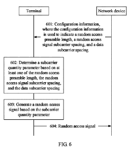
[00138] It should be understood that the embodiment shown in FIG 6 may be
executed by a
terminal, or may be a chip in the terminal. This is not limited in this
application. For ease of
CA 03174302 2022- 9- 29
27
description, the following uses the terminal as an example for description.
However, this
application is not limited thereto.
[00139] 601. The terminal receives configuration information, where the
configuration
information is used to indicate a random access preamble length, a random
access signal
subcarrier spacing, and a data subcarrier spacing.
[00140] Specifically, the terminal may receive the configuration information
from a network
device. Correspondingly, the network device may send the configuration
information to the
terminal. The configuration information may be used to indicate at least one
of the random
access preamble length, the random access signal subcarrier spacing, and the
data subcarrier
spacing.
[00141] It may be understood that, the configuration information may directly
indicate the
random access preamble length. For example, the configuration information
includes the random
access preamble length. Alternatively, the configuration information may
indirectly indicate the
random access preamble length. For example, the configuration information
includes a physical
random access channel configuration index. That is, the terminal may obtain a
random access
preamble format based on the physical random access channel configuration
index, and
correspondingly obtain the random access preamble length. Correspondingly, the
configuration
information may also directly or indirectly indicate the random access signal
subcarrier spacing
or the data subcarrier spacing. For example, the configuration information may
further include a
subcarrier spacing for random access preambles and/or a subcarrier spacing of
an initial uplink
bandwidth part. The subcarrier spacing of the initial uplink bandwidth part is
the data subcarrier
spacing.
[00142] Optionally, the random access preamble length may be any one of 139,
839, 571, or
1151. That is, this application can expand an application range of random
access.
[00143] Optionally, the random access signal subcarrier spacing may be any one
of 1.25 KHz,
5 KHz, 15 KHz, 30 KHz, 60 KHz, 120 KHz, 240 KHz, 480 KHz, 960 KHz, 1920 KHz,
and 3840
KHz.
[00144] Optionally, the data subcarrier spacing may also be any one of 1.25
KHz, 5 KHz, 15
KHz, 30 KHz, 60 KHz, 120 KHz, 240 KHz, 480 KHz, 960 KHz, 1920 KHz, and 3840
KHz.
[00145] It may be understood that a random access signal subcarrier spacing
less than 240
KHz (for example, 1.25 KHz, 5 KHz, 15 KHz, 30 KHz, 60 KHz, or 120 KHz)
corresponds to a
CA 03174302 2022- 9- 29
28
scenario of a carrier frequency band less than 52.6 GHz. A random access
signal subcarrier
spacing greater than or equal to 240 KHz corresponds to a scenario of a
carrier frequency band
greater than or equal to 52.6 GHz.
[00146] Optionally, a data subcarrier spacing less than 240 KHz (for example,
15 KHz, 30
KHz, 60 KHz, or 120 KHz) corresponds to a scenario of a carrier frequency band
less than 52.6
GHz. A data subcarrier spacing greater than or equal to 240 KHz corresponds to
a scenario of a
carrier frequency band greater than or equal to 52.6 GHz.
[00147] 602. The terminal determines a subcarrier quantity parameter based on
at least one of
the random access preamble length, the random access signal subcarrier
spacing, and the data
subcarrier spacing, where the subcarrier quantity parameter includes a first
subcarrier quantity
used to indicate a frequency resource start location of a random access
preamble and a frequency
resource start location of a physical random access channel, and/or a second
subcarrier quantity
used to indicate a frequency resource end location of the random access
preamble and a
frequency resource end location of the physical random access channel.
[00148] Specifically, the terminal may determine the subcarrier quantity
parameter with
reference to at least one of the random access preamble length, the random
access signal
subcarrier spacing, and the data subcarrier spacing. In this way, the terminal
can be helped to
generate an accurate random access signal, thereby helping improve random
access efficiency.
[00149] For example, the terminal may store a mapping relationship of at least
one of the
random access preamble length, the random access signal subcarrier spacing,
and the data
subcarrier spacing with the subcarrier quantity parameter. The mapping
relationship may be
implemented by using a formula, or may be implemented by using a table. This
is not limited in
this application.
[00150] It may be understood that, the frequency resource start location of
the random access
preamble is a start location that is on a subcarrier corresponding to the
physical random access
channel and from which the random access preamble is mapped, and the frequency
resource end
location of the random access preamble is a last location that is on the
subcarrier corresponding
to the physical random access channel and at which the random access preamble
is mapped. The
subcarrier quantity parameter includes the first subcarrier quantity used to
indicate the frequency
resource start location of the random access preamble and the frequency
resource start location
of the physical random access channel, that is, the guard interval 1 shown in
FIG 4 or FIG 5.
CA 03174302 2022- 9- 29
29
The subcarrier quantity parameter may further include the second subcarrier
quantity used to
indicate the frequency resource end location of the random access preamble and
the frequency
resource end location of the physical random access channel, that is, the
guard interval 2 shown
in FIG 4 or FIG 5.
[00151] It should be noted that, the subcarrier quantity parameter may include
only the first
subcarrier quantity, or may include only the second subcarrier quantity, or
may include the first
subcarrier quantity and the second subcarrier quantity. When the subcarrier
quantity parameter
includes only the first subcarrier quantity or the second subcarrier quantity,
the terminal may
derive the other subcarrier quantity with reference to a total subcarrier
quantity (which may also
be referred to as a "total subcarrier quantity width" in the following
embodiment). For example,
the subcarrier quantity includes the first subcarrier quantity, and the
terminal may obtain the
second subcarrier quantity by subtracting the first subcarrier quantity from
the total subcarrier
quantity.
[00152] It may be further understood that the frequency resource may also be
referred to as a
"frequency domain resource", which are not distinguished in the following
embodiment.
[00153] In an embodiment, step 602 may be specifically as follows: The
terminal first
determines a total subcarrier quantity frequency domain width based on the
random access
preamble length, the random access signal subcarrier spacing, and the data
subcarrier spacing in
the configuration information, and then determines the subcarrier quantity
parameter based on
the total subcarrier quantity frequency domain width, the random access signal
subcarrier
spacing, and the data subcarrier spacing.
[00154] Specifically, the total subcarrier quantity frequency domain width may
be a total
frequency domain width occupied by the guard interval 1 and the guard interval
2 that are shown
in FIG 4. That is, the terminal may first determine the total subcarrier
quantity frequency domain
width, and then further determine the subcarrier quantity parameter. In other
words, the terminal
may indirectly obtain the subcarrier quantity parameter.
[00155] Optionally, that the terminal determines a total subcarrier quantity
frequency domain
width based on the random access preamble length, the random access signal
subcarrier spacing,
and the data subcarrier spacing may be specifically as follows:
GP= NRRAB* (Af * N)¨ ',RA* Af RA (2)
CA 03174302 2022- 9- 29
where GP represents the total subcarrier quantity frequency domain width, Af
represents the data subcarrier spacing, AfRA represents the random access
signal subcarrier
spacing, AT:4B represents a total quantity of frequency domain resource blocks
allocated to a
random access signal, N represents a quantity of subcarriers in one RB, and
LRA represents the
random access preamble length. * represents multiplication, and may also be
denoted as x.
[00156] It may be understood that, in NR, a quantity of subcarriers in one RB
may be 12. In
the following embodiment, N=12 is used as an example for description. However,
this
application is not limited thereto.
[00157] It may be understood that AP:AB may be known, or may be determined by
using the
following formula (3), which is not limited in this application:
AT:AB = ceil(L,* Af, I (Af* N))
(3)
where LRA represents the random access preamble length, AT:4B represents the
total
quantity of frequency domain resource blocks allocated to the random access
signal, N
represents the quantity of subcarriers in one RB, Af represents the data
subcarrier spacing,
AfR, represents the random access signal subcarrier spacing, and ceil
represents rounding up.
[00158] For example, if N=12, LRA =139, AfRA =240 KHz, and Af =60 KHz,
AT:AB =ceil(139*240/(60*12))=47, that is, one random access signal occupies 47
RBs in
frequency domain.
[00159] Correspondingly, GP=47*(60*12)-139*240=48000 Hz may be obtained based
on
formula (2).
[00160] It may be further understood that, the terminal may alternatively
directly determine
the subcarrier quantity parameter based on the random access preamble length,
the random
access signal subcarrier spacing, and the data subcarrier spacing, for
example, by using the
following formula (4), that is, the terminal does not need to learn the
intermediate parameter
AT:AB :
GP = ceil(LRA* Af RA I (Af * N))* (Af* N)¨ LRA* Af RA
(4)
CA 03174302 2022- 9- 29
31
where GP represents the total subcarrier quantity frequency domain width, LRA
represents the random access preamble length, NIRL4B represents the total
quantity of frequency
domain resource blocks allocated to the random access signal, N represents the
quantity of
subcarriers in one RB, Af represents the data subcarrier spacing, AfRA
represents the random
access signal subcarrier spacing, and ceil represents rounding up.
[00161] Optionally, the first subcarrier quantity and the second subcarrier
quantity are the
same.
[00162] Specifically, the guard interval 1 and the guard interval 2 may be the
same, so that the
terminal may implement same impact on data demodulation at two ends of the
random access
signal, thereby reducing complexity of the terminal.
[00163] Optionally, when the first subcarrier quantity and the second
subcarrier quantity are
the same, the total subcarrier quantity frequency domain width, the random
access signal
subcarrier spacing, the data subcarrier spacing, and the subcarrier quantity
parameter meet the
following relationship:
, GP Af )
k¨ l
= 2 2 (5)
+0.5
AfRA
where GP represents the total subcarrier quantity frequency domain width, Af
represents the data subcarrier spacing, AfRA represents the random access
signal subcarrier
spacing, and k represents the subcarrier quantity parameter.
[00164] Specifically, as shown in FIG 6, that the guard interval 1 and the
guard interval are
the same means that the guard interval 1 or the guard interval 2 is GP/2, and
GP/2 meets the
following relationship:
GP/2= GP 1 2 = AIR A k ¨ AIR A / 2 + Af / 2
(6)
[00165] In this way, formula (5) may be derived from formula (6).
[00166] It may be understood that any transformation performed on formula (5)
falls within
the protection scope of this application.
[00167] Optionally, the terminal may store the following table (Table 1). For
example, the
random access preamble length may be 139, and a value of k may be shown in the
following
CA 03174302 2022- 9- 29
32
Table 1. In this way, when learning LRA , Af , and AfRA , the terminal may
obtain the value of
k by searching the table.
Table 1
L RA Af RA Af AT:AB k Round Ceil
Floor
139 240 60 47 1.375 1 2
1
139 480 60 93 0.6875 1 1
0
139 960 60 186 0.71875 1 1
0
139 1920 60 371 0.546875 1 1
0
139 3840 60 742 0.554688 1 1
0
139 240 120 24 2.75 3 3
2
139 480 120 47 1.375 1 2
1
139 960 120 93 0.6875 1 1
0
139 1920 120 186 0.71875 1 1
0
139 3840 120 371 0.546875 1 1
0
139 120 240 6 2 2 2
2
139 240 240 12 2.5 3 3
2
139 480 240 24 2.75 3 3
2
139 960 240 47 1.375 1 2
1
139 1920 240 93 0.6875 1 1
0
139 3840 240 186 0.71875 1 1
0
139 120 480 3 1 1 1
1
139 240 480 6 2 2 2
2
139 480 480 12 2.5 3 3
2
139 960 480 24 2.75 3 3
2
139 1920 480 47 1.375 1 2
1
139 3840 480 93 0.6875 1 1
0
139 120 960 2 23 23 23
23
CA 03174302 2022- 9- 29
33
LRA AfRA 4 f N:AB k Round Ceil
Floor
139 240 960 3 1 1 1
1
139 480 960 6 2 2 2
2
139 960 960 12 2.5 3 3
2
139 1920 960 24 2.75 3 3
2
139 3840 960 47 1.375 1 2
1
139 120 1920 1 19 19 19
19
139 240 1920 2 23 23 23
23
139 480 1920 3 1 1 1
1
139 960 1920 6 2 2 2
2
139 1920 1920 12 2.5 3 3
2
139 3840 1920 24 2.75 3 3
2
139 120 3840 1 107 107 107
107
139 240 3840 1 19 19 19
19
139 480 3840 2 23 23 23
23
139 960 3840 3 1 1 1
1
139 1920 3840 6 2 2 2
2
139 3840 3840 12 2.5 3 3
2
[00168] It may be understood that k in Table 1 may be calculated by using
formula (5). The
terminal may learn a calculation manner of formula (5) to obtain Table 1, or
may only store Table
1. This is not limited in this application.
[00169] It may be understood that when the value of k is an integer,
complexity of sending
a signal by the terminal may be reduced. Therefore, in this embodiment of this
application,
rounding (Round) (approximating to the nearest integer), ceiling (rounding
up), or flooring
(rounding down) may be performed on k in Table 1, to obtain an integer as k.
For example,
as shown in the following Table 2, flooring on k is used as an example for
description.
CA 03174302 2022- 9- 29
34
Table 2
L RA Af RA A f NRRA, k
139 240 60 47 1
139 480 60 93 0
139 960 60 186 0
139 1920 60 371 0
139 3840 60 742 0
139 240 120 24 2
139 480 120 47 1
139 960 120 93 0
139 1920 120 186 0
139 3840 120 371 0
139 120 240 6 2
139 240 240 12 2
139 480 240 24 2
139 960 240 47 1
139 1920 240 93 0
139 3840 240 186 0
139 120 480 3 1
139 240 480 6 2
139 480 480 12 2
139 960 480 24 2
139 1920 480 47 1
139 3840 480 93 0
139 120 960 2 23
139 240 960 3 1
139 480 960 6 2
139 960 960 12 2
CA 03174302 2022- 9- 29
LRA AfRA Af N:AB k
139 1920 960 24 2
139 3840 960 47 1
139 120 1920 1 19
139 240 1920 2 23
139 480 1920 3 1
139 960 1920 6 2
139 1920 1920 12 2
139 3840 1920 24 2
139 120 3840 1 107
139 240 3840 1 19
139 480 3840 2 23
139 960 3840 3 1
139 1920 3840 6 2
139 3840 3840 12 2
[00170] It may be further understood that Table 1 may be further simplified
into the following
Table 3.
Table 3
LRA AfRA Af k
139 240 60 1
139 480 60 0
139 960 60 0
139 1920 60 0
139 3840 60 0
139 240 120 2
139 480 120 1
139 960 120 0
CA 03174302 2022- 9- 29
36
LRA Af RA Af k
139 1920 120 0
139 3840 120 0
139 120 240 2
139 240 240 2
139 480 240 2
139 960 240 1
139 1920 240 0
139 3840 240 0
139 120 480 1
139 240 480 2
139 480 480 2
139 960 480 2
139 1920 480 1
139 3840 480 0
139 120 960 23
139 240 960 1
139 480 960 2
139 960 960 2
139 1920 960 2
139 3840 960 1
139 120 1920 19
139 240 1920 23
139 480 1920 1
139 960 1920 2
139 1920 1920 2
139 3840 1920 2
139 120 3840 107
CA 03174302 2022- 9- 29
37
LRA AfRA Af k
139 240 3840 19
139 480 3840 23
139 960 3840 1
139 1920 3840 2
139 3840 3840 2
[00171] It may be further understood that, the terminal may alternatively
store only
correspondences of AfRA = Af , or may store only correspondences of AfRA <Af.
. This is not
limited in this application.
[00172] Optionally, the terminal may store the following table (Table 4). For
example, the
random access preamble length may be 571, and a value of k may be shown in the
following
Table 4.
Table 4
LRA AfRA Af NRRA, k Round Ceil
Floor
571 240 60 191 1.375 1 2
1
571 480 60 381 0.6875 1 1
0
571 960 60 762 0.71875 1 1
0
571 1920 60 1523 0.546875 1 1
0
571 3840 60 3046 0.554688 1 1
0
571 240 120 96 2.75 3 3
2
571 480 120 191 1.375 1 2
1
571 960 120 381 0.6875 1 1
0
571 1920 120 762 0.71875 1 1
0
571 3840 120 1523 0.546875 1 1
0
571 120 240 24 2 2 2
2
571 240 240 48 2.5 3 3
2
571 480 240 96 2.75 3 3
2
CA 03174302 2022- 9- 29
38
LRA AfRA Af N:AB k Round Ceil
Floor
571 960 240 191 1.375 1 2
1
571 1920 240 381 0.6875 1 1
0
571 3840 240 762 0.71875 1 1
0
571 120 480 12 1 1 1
1
571 240 480 24 2 2 2
2
571 480 480 48 2.5 3 3
2
571 960 480 96 2.75 3 3
2
571 1920 480 191 1.375 1 2
1
571 3840 480 381 0.6875 1 1
0
571 120 960 6 ¨1 ¨1 ¨1
¨1
571 240 960 12 1 1 1
1
571 480 960 24 2 2 2
2
571 960 960 48 2.5 3 3
2
571 1920 960 96 2.75 3 3
2
571 3840 960 191 1.375 1 2
1
571 120 1920 3 ¨5 ¨5 ¨5
¨5
571 240 1920 6 ¨1 ¨1 ¨1
¨1
571 480 1920 12 1 1 1
1
571 960 1920 24 2 2 2
2
571 1920 1920 48 2.5 3 3
2
571 3840 1920 96 2.75 3 3
2
571 120 3840 2 83 83 83
83
571 240 3840 3 ¨5 ¨5 ¨5
¨5
571 480 3840 6 ¨1 ¨1 ¨1
¨1
571 960 3840 12 1 1 1
1
571 1920 3840 24 2 2 2
2
571 3840 3840 48 2.5 3 3
2
CA 03174302 2022- 9- 29
39
[00173] It may be understood that, for correspondences of LRA =571 stored in
the terminal,
refer to transformations shown in Table 1 to Table 2 or Table 3 and other
transformations of
Table 1. This is not limited in this application.
[00174] Optionally, the terminal may store the following table (Table 5). For
example, the
random access preamble length may be 1151, and a value of k may be shown in
the following
Table 5.
Table 5
LRA AfRA Af NRR A , k Round Ceil
Floor
1151 240 60 384 0.875 1 1
0
1151 480 60 768 0.9375 1 1
0
1151 960 60 1535 0.59375 1 1
0
1151 1920 60 3070 0.609375 1 1
0
1151 3840 60 6139 0.523438 1 1
0
1151 240 120 192 0.75 1 1
0
1151 480 120 384 0.875 1 1
0
1151 960 120 768 0.9375 1 1
0
1151 1920 120 1535 0.59375 1 1
0
1151 3840 120 3070 0.609375 1 1
0
1151 120 240 48 0 0 0
0
1151 240 240 96 0.5 1 1
0
1151 480 240 192 0.75 1 1
0
1151 960 240 384 0.875 1 1
0
1151 1920 240 768 0.9375 1 1
0
1151 3840 240 1535 0.59375 1 1
0
1151 120 480 24 ¨1 ¨1 ¨1
¨1
1151 240 480 48 0 0 0
0
1151 480 480 96 0.5 1 1
0
1151 960 480 192 0.75 1 1
0
CA 03174302 2022- 9- 29
LRA AfRA A f NRRA, k Round Ceil
Floor
1151 1920 480 384 0.875 1 1
0
1151 3840 480 768 0.9375 1 1
0
1151 120 960 12 ¨3 ¨3 ¨3
¨3
1151 240 960 24 ¨1 ¨1 ¨1
¨1
1151 480 960 48 0 0 0
0
1151 960 960 96 0.5 1 1
0
1151 1920 960 192 0.75 1 1
0
1151 3840 960 384 0.875 1 1
0
1151 120 1920 6 ¨7 ¨7 ¨7
¨7
1151 240 1920 12 ¨3 ¨3 ¨3
¨3
1151 480 1920 24 ¨1 ¨1 ¨1
¨1
1151 960 1920 48 0 0 0
0
1151 1920 1920 96 0.5 1 1
0
1151 3840 1920 192 0.75 1 1
0
1151 120 3840 3 ¨15 ¨15 ¨15
¨15
1151 240 3840 6 ¨7 ¨7 ¨7
¨7
1151 480 3840 12 ¨3 ¨3 ¨3
¨3
1151 960 3840 24 ¨1 ¨1 ¨1
¨1
1151 1920 3840 48 0 0 0
0
1151 3840 3840 96 0.5 1 1
0
[00175] It may be understood that, the terminal may alternatively store
correspondences for a
plurality of L. . For example, the terminal may store a table that includes
all content shown in
Table 1, Table 4, and Table 5. This is not limited in this application.
[00176] In addition, the terminal may alternatively store only correspondences
for AfRA =Af
in the plurality of ',RA , for example, as shown in Table 6 (using an example
in which the value
of k is rounded) and Table 7 (using an example in which the value of k is
floored).
CA 03174302 2022- 9- 29
41
Alternatively, the terminal stores only correspondences for AfRA <Af in the
plurality of LRA ,
for example, as shown in Table 8 (using an example in which the value of k is
rounded).
Table 6
LRA AfRA Af k
139 240 240 3
139 480 480 3
139 960 960 3
139 1920 1920 3
139 3840 3840 3
571 240 240 3
571 960 960 3
571 1920 1920 3
571 3840 3840 3
1151 480 480 1
1151 960 960 1
1151 1920 1920 1
1151 3840 3840 1
Table 7
LRA AfRA Af k
139 240 240 2
139 480 480 2
139 960 960 2
139 1920 1920 2
139 3840 3840 2
571 240 240 2
CA 03174302 2022- 9- 29
42
LRA AfRA Af k
571 960 960 2
571 1920 1920 2
571 3840 3840 2
1151 480 480 0
1151 960 960 0
1151 1920 1920 0
1151 3840 3840 0
Table 8
LRA AfRA Af k
139 120 240 2
139 120 480 1
139 240 480 2
139 120 960 23
139 240 960 1
139 480 960 2
139 120 1920 19
139 240 1920 23
139 480 1920 1
139 960 1920 2
139 120 3840 107
139 240 3840 19
139 480 3840 23
139 960 3840 1
139 1920 3840 2
571 120 240 2
571 120 480 1
CA 03174302 2022- 9- 29
43
LRA AfRA Af k
571 240 480 2
571 120 960 -1
571 240 960 1
571 480 960 2
571 120 1920 -5
571 240 1920 -1
571 480 1920 1
571 960 1920 2
571 120 3840 83
571 240 3840 -5
571 480 3840 -1
571 960 3840 1
571 1920 3840 2
1151 120 240 0
1151 120 480 -1
1151 240 480 0
1151 120 960 -3
1151 240 960 -1
1151 480 960 0
1151 120 1920 -7
1151 240 1920 -3
1151 480 1920 -1
1151 960 1920 0
1151 120 3840 -15
1151 240 3840 -7
1151 480 3840 -3
1151 960 3840 -1
CA 03174302 2022- 9- 29
44
LRA AfRA Af k
1151 1920 3840 0
[00177] It should be understood that the terminal may store a table that is
any combination or
any transformation of the foregoing tables. This is not limited in this
application. For example,
the terminal may store only values of parameters supported by the network
device or the
terminal.
[00178] It may be understood that, as shown in Table 6 to Table 8, the value
of k may be
any one of ¨15, ¨7, ¨5, ¨3, ¨1, 0, 1, 2, 3, 19, 23, 83, and 107.
[00179] Optionally, the first subcarrier quantity and the total subcarrier
quantity frequency
domain width may be the same, and the second subcarrier quantity is zero.
[00180] Specifically, the guard intervals of the random access signal may be
set to a
maximum at one end and zero at the other end. In this way, impact on other
frequency division
data may be minimized by the end with a maximum guard interval, thereby
improving data
demodulation performance. In addition, for the end with a guard interval of
zero, the network
device may reduce interference by performing scheduling to avoid data
transmission or
scheduling low MCS data.
[00181] Optionally, when the second subcarrier quantity is 0, that is, when
the guard interval 2
shown in FIG 4 is 0, the random access signal subcarrier spacing, the data
subcarrier spacing,
and the subcarrier quantity parameter meet the following relationship:
(GP¨ Af)
k = 2 +0.5
(7)
AfRA
where GP represents the total subcarrier quantity frequency domain width, Af
represents the data subcarrier spacing, AfRA represents the random access
signal subcarrier
spacing, and k represents the subcarrier quantity parameter.
[00182] Specifically, when ',RA =139, correspondences for ',RA =139 may be
shown in the
following Table 9, correspondences for Liu =571 may be shown in the following
Table 10, and
correspondences between ',RA =1151 may be shown in the following Table 11.
CA 03174302 2022- 9- 29
[00183] It may be understood that, the terminal may store a table that is any
combination or
any transformation of Table 9 to Table 11. This is not limited in this
application.
[00184] Optionally, when the second subcarrier quantity is 0, that is, when
the guard interval 2
shown in FIG 4 is 0, the random access signal subcarrier spacing, the data
subcarrier spacing,
and the subcarrier quantity parameter may alternatively meet the following
relationship:
(GP + Af)
k = 2 +0.5 (8)
AfRA
where GP represents the total subcarrier quantity frequency domain width, Af
represents the data subcarrier spacing, AfRA represents the random access
signal subcarrier
spacing, and k represents the subcarrier quantity parameter.
Table 9
L RA Af RA Af N:AB k Round Ceil
Floor
139 240 60 47 2.375 2 3
2
139 480 60 93 0.9375 1 1
0
139 960 60 186 0.96875 1 1
0
139 1920 60 371 0.609375 1 1
0
139 3840 60 742 0.617188 1 1
0
139 240 120 24 5.25 5 6
5
139 480 120 47 2.375 2 3
2
139 960 120 93 0.9375 1 1
0
139 1920 120 186 0.96875 1 1
0
139 3840 120 371 0.609375 1 1
0
139 120 240 6 4.5 5 5
4
139 240 240 12 5 5 5
5
139 480 240 24 5.25 5 6
5
139 960 240 47 2.375 2 3
2
CA 03174302 2022- 9- 29
46
LRA AfRA Af N:AB k Round Ceil
Floor
139 1920 240 93 0.9375 1 1
0
139 3840 240 186 0.96875 1 1
0
139 120 480 3 3.5 4 4
3
139 240 480 6 4.5 5 5
4
139 480 480 12 5 5 5
5
139 960 480 24 5.25 5 6
5
139 1920 480 47 2.375 2 3
2
139 3840 480 93 0.9375 1 1
0
139 120 960 2 49.5 50 50
49
139 240 960 3 3.5 4 4
3
139 480 960 6 4.5 5 5
4
139 960 960 12 5 5 5
5
139 1920 960 24 5.25 5 6
5
139 3840 960 47 2.375 2 3
2
139 120 1920 1 45.5 46 46
45
139 240 1920 2 49.5 50 50
49
139 480 1920 3 3.5 4 4
3
139 960 1920 6 4.5 5 5
4
139 1920 1920 12 5 5 5
5
139 3840 1920 24 5.25 5 6
5
139 120 3840 1 229.5 230 230
229
139 240 3840 1 45.5 46 46
45
139 480 3840 2 49.5 50 50
49
139 960 3840 3 3.5 4 4
3
139 1920 3840 6 4.5 5 5
4
139 3840 3840 12 5 5 5
5
CA 03174302 2022- 9- 29
47
Table 10
LRA AfRA Af NRR A , k Round Ceil
Floor
571 240 60 191 2.375 2 3
2
571 480 60 381 0.9375 1 1
0
571 960 60 762 0.96875 1 1
0
571 1920 60 1523 0.609375 1 1
0
571 3840 60 3046 0.617188 1 1
0
571 240 120 96 5.25 5 6
5
571 480 120 191 2.375 2 3
2
571 960 120 381 0.9375 1 1
0
571 1920 120 762 0.96875 1 1
0
571 3840 120 1523 0.609375 1 1
0
571 120 240 24 4.5 5 5
4
571 240 240 48 5 5 5
5
571 480 240 96 5.25 5 6
5
571 960 240 191 2.375 2 3
2
571 1920 240 381 0.9375 1 1
0
571 3840 240 762 0.96875 1 1
0
571 120 480 12 3.5 4 4
3
571 240 480 24 4.5 5 5
4
571 480 480 48 5 5 5
5
571 960 480 96 5.25 5 6
5
571 1920 480 191 2.375 2 3
2
571 3840 480 381 0.9375 1 1
0
571 120 960 6 1.5 2 2
1
571 240 960 12 3.5 4 4
3
571 480 960 24 4.5 5 5
4
571 960 960 48 5 5 5
5
CA 03174302 2022- 9- 29
48
LRA AfRA Af N:AB k Round Ceil
Floor
571 1920 960 96 5.25 5 6
5
571 3840 960 191 2.375 2 3
2
571 120 1920 3 ¨2.5 ¨3 ¨2
¨3
571 240 1920 6 1.5 2 2
1
571 480 1920 12 3.5 4 4
3
571 960 1920 24 4.5 5 5
4
571 1920 1920 48 5 5 5
5
571 3840 1920 96 5.25 5 6
5
571 120 3840 2 181.5 182 182
181
571 240 3840 3 ¨2.5 ¨3 ¨2
¨3
571 480 3840 6 1.5 2 2
1
571 960 3840 12 3.5 4 4
3
571 1920 3840 24 4.5 5 5
4
571 3840 3840 48 5 5 5
5
Table 11
LRA AfRA Af NRRAB k Round Ceil
Floor
1151 240 60 384 1.375 1 2
1
1151 480 60 768 1.4375 1 2
1
1151 960 60 1535 0.71875 1 1
0
1151 1920 60 3070 0.734375 1 1
0
1151 3840 60 6139 0.554688 1 1
0
1151 240 120 192 1.25 1 2
1
1151 480 120 384 1.375 1 2
1
1151 960 120 768 1.4375 1 2
1
1151 1920 120 1535 0.71875 1 1
0
CA 03174302 2022- 9- 29
49
LRA AfRA Af N:AB k Round Ceil
Floor
1151 3840 120 3070 0.734375 1 1
0
1151 120 240 48 0.5 1 1
0
1151 240 240 96 1 1 1
1
1151 480 240 192 1.25 1 2
1
1151 960 240 384 1.375 1 2
1
1151 1920 240 768 1.4375 1 2
1
1151 3840 240 1535 0.71875 1 1
0
1151 120 480 24 ¨0.5 ¨1 0
¨1
1151 240 480 48 0.5 1 1
0
1151 480 480 96 1 1 1
1
1151 960 480 192 1.25 1 2
1
1151 1920 480 384 1.375 1 2
1
1151 3840 480 768 1.4375 1 2
1
1151 120 960 12 ¨2.5 ¨3 ¨2
¨3
1151 240 960 24 ¨0.5 ¨1 0
¨1
1151 480 960 48 0.5 1 1
0
1151 960 960 96 1 1 1
1
1151 1920 960 192 1.25 1 2
1
1151 3840 960 384 1.375 1 2
1
1151 120 1920 6 ¨6.5 ¨7 ¨6
¨7
1151 240 1920 12 ¨2.5 ¨3 ¨2
¨3
1151 480 1920 24 ¨0.5 ¨1 0
¨1
1151 960 1920 48 0.5 1 1
0
1151 1920 1920 96 1 1 1
1
1151 3840 1920 192 1.25 1 2
1
1151 120 3840 3 ¨14.5 ¨15 ¨14
¨15
1151 240 3840 6 ¨6.5 ¨7 ¨6 ¨7
CA 03174302 2022- 9- 29
LRA Af RA Af N:AB k Round Ceil
Floor
1151 480 3840 12 ¨2.5 ¨3 ¨2
¨3
1151 960 3840 24 ¨0.5 ¨1 0
¨1
1151 1920 3840 48 0.5 1 1
0
1151 3840 3840 96 1 1 1
1
[00185] In another embodiment, step 602 may be specifically as follows: The
terminal
directly determines the subcarrier quantity parameter based on the random
access signal
subcarrier spacing and the data subcarrier spacing in the configuration
information.
[00186] Specifically, the terminal may determine the subcarrier quantity
parameter with
reference to the random access signal subcarrier spacing and the data
subcarrier spacing. For
example, the terminal may store a mapping relationship of the random access
signal subcarrier
spacing and the data subcarrier spacing with the subcarrier quantity
parameter. The mapping
relationship may be implemented by using a formula, or may be implemented by
using a table.
This is not limited in this application.
[00187] Optionally, the second subcarrier quantity and the total subcarrier
quantity frequency
domain width may be the same, and the first subcarrier quantity is zero.
[00188] Optionally, when the first subcarrier quantity is 0, that is, when the
guard interval 1
shown in FIG 4 is 0, the random access signal subcarrier spacing, the data
subcarrier spacing,
and the subcarrier quantity parameter meet the following relationship:
(0 ¨ Af )
2 k (9) =
_______________________________________________ + 0.5
AfRA
where Af represents the data subcarrier spacing, AfRA represents the random
access signal subcarrier spacing, and k represents the subcarrier quantity
parameter.
[00189] Specifically, the terminal determines a value of k based on formula
(9), that is, the
terminal moves a location of a subcarrier to which the random access preamble
is mapped
toward a center of the random access channel, thereby helping reduce
interference with another
data channel.
[00190] Optionally, the random access signal subcarrier spacing, the data
subcarrier spacing,
CA 03174302 2022- 9- 29
51
and the subcarrier quantity parameter may alternatively meet the following
relationship:
k = Af +0.5
(10)
2AfRA
[00191] Specifically, the terminal determines a value of k based on formula
(10), that is, the
terminal moves a location of a subcarrier to which the random access preamble
is mapped
toward a center of the random access channel, thereby helping reduce
interference with another
data channel.
[00192] Specifically, when ',RA =139, correspondences for LRA =139 may be
shown in the
following Table 12 or Table 13, correspondences for ',RA =571 may be shown in
the following
Table 14 or Table 15, and correspondences between ',RA =1151 may be shown in
the following
Table 16 or Table 17.
[00193] It may be understood that, the terminal may store a table that is any
combination or
any transformation of either Table 12 or Table 13, either Table 14 or Table
15, and either Table
16 or Table 17. This is not limited in this application.
[00194] It should be noted that Table 12, Table 14, and Table 16 may be
obtained by
calculation based on formula (9), and Table 13, Table 15, and Table 17 may be
obtained by
calculation based on formula (10).
Table 12
LRA AfRA Af NRRAB k Round Ceil
Floor
139 240 60 47 0.375 0 1
0
139 480 60 93 0.4375 0 1
0
139 960 60 186 0.46875 0 1
0
139 1920 60 371 0.484375 0 1
0
139 3840 60 742 0.492188 0 1
0
139 240 120 24 0.25 0 1
0
139 480 120 47 0.375 0 1
0
139 960 120 93 0.4375 0 1
0
CA 03174302 2022- 9- 29
52
LRA AfRA Af N:AB k Round Ceil
Floor
139 1920 120 186 0.46875 0 1
0
139 3840 120 371 0.484375 0 1
0
139 120 240 6 ¨0.5 ¨1 0
¨1
139 240 240 12 0 0 0
0
139 480 240 24 0.25 0 1
0
139 960 240 47 0.375 0 1
0
139 1920 240 93 0.4375 0 1
0
139 3840 240 186 0.46875 0 1
0
139 120 480 3 ¨1.5 ¨2 ¨1
¨2
139 240 480 6 ¨0.5 ¨1 0
¨1
139 480 480 12 0 0 0
0
139 960 480 24 0.25 0 1
0
139 1920 480 47 0.375 0 1
0
139 3840 480 93 0.4375 0 1
0
139 120 960 2 ¨3.5 ¨4 ¨3
¨4
139 240 960 3 ¨1.5 ¨2 ¨1
¨2
139 480 960 6 ¨0.5 ¨1 0
¨1
139 960 960 12 0 0 0
0
139 1920 960 24 0.25 0 1
0
139 3840 960 47 0.375 0 1
0
139 120 1920 1 ¨7.5 ¨8 ¨7
¨8
139 240 1920 2 ¨3.5 ¨4 ¨3
¨4
139 480 1920 3 ¨1.5 ¨2 ¨1
¨2
139 960 1920 6 ¨0.5 ¨1 0
¨1
139 1920 1920 12 0 0 0
0
139 3840 1920 24 0.25 0 1
0
139 120 3840 1 ¨15.5 ¨16 ¨15
¨16
CA 03174302 2022- 9- 29
53
LRA AfRA Af N:AB k Round Ceil
Floor
139 240 3840 1 ¨7.5 ¨8 ¨7
¨8
139 480 3840 2 ¨3.5 ¨4 ¨3
¨4
139 960 3840 3 ¨1.5 ¨2 ¨1
¨2
139 1920 3840 6 ¨0.5 ¨1 0
¨1
139 3840 3840 12 0 0 0
0
Table 13
LRA AfRA .A.f NRRAB k Round Ceil
Floor
139 240 60 47 0.625 1 1
0
139 480 60 93 0.5625 1 1
0
139 960 60 186 0.53125 1 1
0
139 1920 60 371 0.515625 1 1
0
139 3840 60 742 0.5078125 1 1
0
139 240 120 24 0.75 1 1
0
139 480 120 47 0.625 1 1
0
139 960 120 93 0.5625 1 1
0
139 1920 120 186 0.53125 1 1
0
139 3840 120 371 0.515625 1 1
0
139 120 240 6 1.5 2 2
1
139 240 240 12 1 1 1
1
139 480 240 24 0.75 1 1
0
139 960 240 47 0.625 1 1
0
139 1920 240 93 0.5625 1 1
0
139 3840 240 186 0.53125 1 1
0
139 120 480 3 2.5 3 3
2
139 240 480 6 1.5 2 2
1
CA 03174302 2022- 9- 29
54
LRA AfRA Af N:AB k Round Ceil
Floor
139 480 480 12 1 1 1
1
139 960 480 24 0.75 1 1
0
139 1920 480 47 0.625 1 1
0
139 3840 480 93 0.5625 1 1
0
139 120 960 2 4.5 5 5
4
139 240 960 3 2.5 3 3
2
139 480 960 6 1.5 2 2
1
139 960 960 12 1 1 1
1
139 1920 960 24 0.75 1 1
0
139 3840 960 47 0.625 1 1
0
139 120 1920 1 8.5 9 9
8
139 240 1920 2 4.5 5 5
4
139 480 1920 3 2.5 3 3
2
139 960 1920 6 1.5 2 2
1
139 1920 1920 12 1 1 1
1
139 3840 1920 24 0.75 1 1
0
139 120 3840 1 16.5 17 17
16
139 240 3840 1 8.5 9 9
8
139 480 3840 2 4.5 5 5
4
139 960 3840 3 2.5 3 3
2
139 1920 3840 6 1.5 2 2
1
139 3840 3840 12 1 1 1
1
Table 14
LRA AfRA Af NRRAB k Round Ceil
Floor
571 240 60 191 0.375 0 1
0
CA 03174302 2022- 9- 29
LRA AfRA Af N:AB k Round Ceil
Floor
571 480 60 381 0.4375 0 1
0
571 960 60 762 0.46875 0 1
0
571 1920 60 1523 0.484375 0 1
0
571 3840 60 3046 0.492188 0 1
0
571 240 120 96 0.25 0 1
0
571 480 120 191 0.375 0 1
0
571 960 120 381 0.4375 0 1
0
571 1920 120 762 0.46875 0 1
0
571 3840 120 1523 0.484375 0 1
0
571 120 240 24 ¨0.5 ¨1 0
¨1
571 240 240 48 0 0 0
0
571 480 240 96 0.25 0 1
0
571 960 240 191 0.375 0 1
0
571 1920 240 381 0.4375 0 1
0
571 3840 240 762 0.46875 0 1
0
571 120 480 12 ¨1.5 ¨2 ¨1
¨2
571 240 480 24 ¨0.5 ¨1 0
¨1
571 480 480 48 0 0 0
0
571 960 480 96 0.25 0 1
0
571 1920 480 191 0.375 0 1
0
571 3840 480 381 0.4375 0 1
0
571 120 960 6 ¨3.5 ¨4 ¨3
¨4
571 240 960 12 ¨1.5 ¨2 ¨1
¨2
571 480 960 24 ¨0.5 ¨1 0
¨1
571 960 960 48 0 0 0
0
571 1920 960 96 0.25 0 1
0
571 3840 960 191 0.375 0 1
0
CA 03174302 2022- 9- 29
56
LRA AfRA Af N:AB k Round Ceil
Floor
571 120 1920 3 ¨7.5 ¨8 ¨7
¨8
571 240 1920 6 ¨3.5 ¨4 ¨3
¨4
571 480 1920 12 ¨1.5 ¨2 ¨1
¨2
571 960 1920 24 ¨0.5 ¨1 0
¨1
571 1920 1920 48 0 0 0
0
571 3840 1920 96 0.25 0 1
0
571 120 3840 2 ¨15.5 ¨16 ¨15
¨16
571 240 3840 3 ¨7.5 ¨8 ¨7
¨8
571 480 3840 6 ¨3.5 ¨4 ¨3
¨4
571 960 3840 12 ¨1.5 ¨2 ¨1
¨2
571 1920 3840 24 ¨0.5 ¨1 0
¨1
571 3840 3840 48 0 0 0
0
Table 15
LRA AfRA .A.f N:AB k Round Ceil
Floor
571 240 60 191 0.625 1 1
0
571 480 60 381 0.5625 1 1
0
571 960 60 762 0.53125 1 1
0
571 1920 60 1523 0.515625 1 1
0
571 3840 60 3046 0.5078125 1 1
0
571 240 120 96 0.75 1 1
0
571 480 120 191 0.625 1 1
0
571 960 120 381 0.5625 1 1
0
571 1920 120 762 0.53125 1 1
0
571 3840 120 1523 0.515625 1 1
0
571 120 240 24 1.5 2 2
1
CA 03174302 2022- 9- 29
57
LRA AfRA Af N:AB k Round Ceil
Floor
571 240 240 48 1 1 1
1
571 480 240 96 0.75 1 1
0
571 960 240 191 0.625 1 1
0
571 1920 240 381 0.5625 1 1
0
571 3840 240 762 0.53125 1 1
0
571 120 480 12 2.5 3 3
2
571 240 480 24 1.5 2 2
1
571 480 480 48 1 1 1
1
571 960 480 96 0.75 1 1
0
571 1920 480 191 0.625 1 1
0
571 3840 480 381 0.5625 1 1
0
571 120 960 6 4.5 5 5
4
571 240 960 12 2.5 3 3
2
571 480 960 24 1.5 2 2
1
571 960 960 48 1 1 1
1
571 1920 960 96 0.75 1 1
0
571 3840 960 191 0.625 1 1
0
571 120 1920 3 8.5 9 9
8
571 240 1920 6 4.5 5 5
4
571 480 1920 12 2.5 3 3
2
571 960 1920 24 1.5 2 2
1
571 1920 1920 48 1 1 1
1
571 3840 1920 96 0.75 1 1
0
571 120 3840 2 16.5 17 17
16
571 240 3840 3 8.5 9 9
8
571 480 3840 6 4.5 5 5
4
571 960 3840 12 2.5 3 3
2
CA 03174302 2022- 9- 29
58
LRA AfRA Af N:AB k Round Ceil
Floor
571 1920 3840 24 1.5 2 2
1
571 3840 3840 48 1 1 1
1
Table 16
LRA AfRA Af N:AB k Round Ceil
Floor
1151 240 60 384 0.375 0 1
0
1151 480 60 768 0.4375 0 1
0
1151 960 60 1535 0.46875 0 1
0
1151 1920 60 3070 0.484375 0 1
0
1151 3840 60 6139 0.492188 0 1
0
1151 240 120 192 0.25 0 1
0
1151 480 120 384 0.375 0 1
0
1151 960 120 768 0.4375 0 1
0
1151 1920 120 1535 0.46875 0 1
0
1151 3840 120 3070 0.484375 0 1
0
1151 120 240 48 ¨0.5 ¨1 0
¨1
1151 240 240 96 0 0 0 0
1151 480 240 192 0.25 0 1
0
1151 960 240 384 0.375 0 1
0
1151 1920 240 768 0.4375 0 1
0
1151 3840 240 1535 0.46875 0 1
0
1151 120 480 24 ¨1.5 ¨2 ¨1
¨2
1151 240 480 48 ¨0.5 ¨1 0
¨1
1151 480 480 96 0 0 0
0
1151 960 480 192 0.25 0 1
0
1151 1920 480 384 0.375 0 1
0
CA 03174302 2022- 9- 29
59
LRA AfRA Af N:AB k Round Ceil
Floor
1151 3840 480 768 0.4375 0 1
0
1151 120 960 12 ¨3.5 ¨4 ¨3
¨4
1151 240 960 24 ¨1.5 ¨2 ¨1
¨2
1151 480 960 48 ¨0.5 ¨1 0
¨1
1151 960 960 96 0 0 0
0
1151 1920 960 192 0.25 0 1
0
1151 3840 960 384 0.375 0 1
0
1151 120 1920 6 ¨7.5 ¨8 ¨7
¨8
1151 240 1920 12 ¨3.5 ¨4 ¨3
¨4
1151 480 1920 24 ¨1.5 ¨2 ¨1
¨2
1151 960 1920 48 ¨0.5 ¨1 0
¨1
1151 1920 1920 96 0 0 0
0
1151 3840 1920 192 0.25 0 1
0
1151 120 3840 3 ¨15.5 ¨16 ¨15
¨16
1151 240 3840 6 ¨7.5 ¨8 ¨7
¨8
1151 480 3840 12 ¨3.5 ¨4 ¨3
¨4
1151 960 3840 24 ¨1.5 ¨2 ¨1
¨2
1151 1920 3840 48 ¨0.5 ¨1 0
¨1
1151 3840 3840 96 0 0 0
0
Table 17
LRA AfRA Af N:AB k Round Ceil
Floor
1151 240 60 384 0.625 1 1
0
1151 480 60 768 0.5625 1 1
0
1151 960 60 1535 0.53125 1 1
0
1151 1920 60 3070 0.515625 1 1
0
CA 03174302 2022- 9- 29
LRA AfRA Af N:AB k Round Ceil
Floor
1151 3840 60 6139 0.5078125 1 1
0
1151 240 120 192 0.75 1 1
0
1151 480 120 384 0.625 1 1
0
1151 960 120 768 0.5625 1 1
0
1151 1920 120 1535 0.53125 1 1
0
1151 3840 120 3070 0.515625 1 1
0
1151 120 240 48 1.5 2 2
1
1151 240 240 96 1 1 1
1
1151 480 240 192 0.75 1 1
0
1151 960 240 384 0.625 1 1
0
1151 1920 240 768 0.5625 1 1
0
1151 3840 240 1535 0.53125 1 1
0
1151 120 480 24 2.5 3 3
2
1151 240 480 48 1.5 2 2
1
1151 480 480 96 1 1 1
1
1151 960 480 192 0.75 1 1
0
1151 1920 480 384 0.625 1 1
0
1151 3840 480 768 0.5625 1 1
0
1151 120 960 12 4.5 5 5
4
1151 240 960 24 2.5 3 3
2
1151 480 960 48 1.5 2 2
1
1151 960 960 96 1 1 1
1
1151 1920 960 192 0.75 1 1
0
1151 3840 960 384 0.625 1 1
0
1151 120 1920 6 8.5 9 9
8
1151 240 1920 12 4.5 5 5
4
1151 480 1920 24 2.5 3 3
2
CA 03174302 2022- 9- 29
61
LRA Af RA Af N:AB k Round Ceil
Floor
1151 960 1920 48 1.5 2 2
1
1151 1920 1920 96 1 1 1
1
1151 3840 1920 192 0.75 1 1
0
1151 120 3840 3 16.5 17 17
16
1151 240 3840 6 8.5 9 9
8
1151 480 3840 12 4.5 5 5
4
1151 960 3840 24 2.5 3 3
2
1151 1920 3840 48 1.5 2 2
1
1151 3840 3840 96 1 1 1
1
[00195] 603. The terminal generates a random access signal based on the
subcarrier quantity
parameter.
[00196] Specifically, the terminal may generate the random access signal based
on the
subcarrier quantity parameter and a random access formula. The random access
formula may be
shown in formula (1).
[00197] It may be understood that any transformation may be performed on
formula (1), and
falls within the protection scope of this application. In addition, the random
access formula for
generating the random access signal by the terminal may alternatively be
another formula. This
is not limited in this application.
[00198] 604. The terminal sends the random access signal.
[00199] Specifically, the terminal may send the random access signal to the
network device.
Correspondingly, the network device may receive the random access signal from
the terminal. If
the terminal sends the random access signal generated based on formula (1),
the terminal may
send the random access signal through an antenna port p.
[00200] Therefore, in this embodiment of this application, the terminal
receives the
configuration information, and determines the subcarrier quantity parameter
with reference to at
least one of the random access preamble length, the random access signal
subcarrier spacing, and
the data subcarrier spacing that are indicated by the configuration
information. In this way, the
terminal can generate an accurate random access signal, thereby improving
random access
CA 03174302 2022- 9- 29
62
efficiency.
[00201] The embodiments described in this specification may be independent
solutions, or
may be combined based on intrinsic logic. These solutions all fall within the
protection scope of
this application.
[00202] It may be understood that, in the foregoing method embodiments,
methods and
operations implemented by the terminal may alternatively be implemented by a
component (for
example, a chip or a circuit) that can be applied to the terminal, and methods
and operations
implemented by the network device may alternatively be implemented by a
component (for
example, a chip or a circuit) that can be applied to the network device.
[00203] The foregoing mainly describes the solutions provided in embodiments
of this
application from the perspective of interaction between network elements. It
may be understood
that, to implement the foregoing functions, each network element, such as the
transmit end
device or the receive end device, includes a corresponding hardware structure
and/or software
module for performing each function. A person skilled in the art should be
aware that units,
algorithms, and steps in the examples described with reference to the
embodiments disclosed in
this specification can be implemented in a form of hardware or a combination
of hardware and
computer software in this application. Whether a function is performed by
hardware or hardware
driven by computer software depends on a particular application and a design
constraint of the
technical solutions. A person skilled in the art may use different methods to
implement the
described functions for each particular application, but it should not be
considered that the
implementation goes beyond the scope of this application.
[00204] In embodiments of this application, function module division may be
performed on
the transmit end device or the receive end device based on the foregoing
method examples. For
example, each function module may be obtained through division corresponding
to each function,
or two or more functions may be integrated into one processing module. The
integrated module
may be implemented in a form of hardware, or may be implemented in a form of a
software
functional module. It should be noted that, in embodiments of this
application, division into the
modules is an example and is merely logical function division, and may be
other division in
actual implementation. The following provides a description by using an
example in which each
function module is obtained through division corresponding to each function.
[00205] It should be understood that specific examples in embodiments of this
application are
CA 03174302 2022- 9- 29
63
merely intended to help a person skilled in the art better understand the
embodiments of this
application, but are not intended to limit the scope of the embodiments of
this application.
[00206] It should be understood that sequence numbers of the foregoing
processes do not
mean execution sequences in embodiments of this application. The execution
sequences of the
processes should be determined based on functions and internal logic of the
processes, and
should not constitute any limitation on implementation processes of the
embodiments of this
application.
[00207] The method provided in the embodiments of this application is
described above in
detail with reference to FIG 4 to FIG 7. The apparatus provided in the
embodiments of this
application is described below in detail with reference to FIG 8 to FIG 15. It
should be
understood that the description of the apparatus embodiments corresponds to
the description of
the method embodiments. Therefore, for content that is not described in
detail, refer to the
foregoing method embodiments. For brevity, details are not described herein
again.
[00208] FIG 8 is a schematic block diagram of an apparatus 800 for
transmitting a random
access signal according to an embodiment of this application.
[00209] It should be understood that, the apparatus 800 may correspond to each
terminal or a
chip in the terminal shown in FIG 1, or the terminal or a chip in the terminal
in the embodiment
shown in FIG 6, and may have any function of the terminal in the method
embodiment shown in
FIG 6. For example, the apparatus 800 includes a transceiver module 810 and a
processing
module 820.
[00210] The transceiver module 810 is configured to receive configuration
information, where
the configuration information is used to indicate a random access preamble
length, a random
access signal subcarrier spacing, and a data subcarrier spacing.
[00211] The processing module 820 is configured to determine a subcarrier
quantity
parameter based on at least one of the random access preamble length, the
random access signal
subcarrier spacing, and the data subcarrier spacing, where the subcarrier
quantity parameter
includes a first subcarrier quantity used to indicate a frequency resource
start location of a
random access preamble and a frequency resource start location of a physical
random access
channel, and/or a second subcarrier quantity used to indicate a frequency
resource end location
of the random access preamble and a frequency resource end location of the
physical random
access channel.
CA 03174302 2022- 9- 29
64
[00212] The processing module 820 is further configured to generate a random
access signal
based on the subcarrier quantity parameter.
[00213] The transceiver module 810 is further configured to send the random
access signal.
[00214] Optionally, a value of the random access signal subcarrier spacing is
any one of 120
kHz, 240 kHz, 480 kHz, 960 kHz, 1920 kHz, and 3840 kHz.
[00215] Optionally, a value of the data subcarrier spacing is any one of 240
kHz, 480 kHz,
960 kHz, 1920 kHz, and 3840 kHz.
[00216] Optionally, a value of the subcarrier quantity parameter is any one of
¨15, ¨7, ¨5, ¨3,
¨1,0, 1, 2, 3, 19, 23, 83, and 107.
[00217] Optionally, the processing module 820 is specifically configured to:
determine a total subcarrier quantity frequency domain width based on the
random
access preamble length, the random access signal subcarrier spacing, and the
data subcarrier
spacing; and
determine the subcarrier quantity parameter based on the total subcarrier
quantity
frequency domain width, the random access signal subcarrier spacing, and the
data subcarrier
spacing.
[00218] Optionally, the processing module 820 is specifically configured to:
determine the subcarrier quantity parameter in the second target parameter
based on
the random access signal subcarrier spacing and the data subcarrier spacing in
the first target
parameter.
[00219] Optionally, the first subcarrier quantity and the second subcarrier
quantity are the
same.
[00220] Optionally, the subcarrier quantity parameter k conforms to:
(GP Af )
k= 2 2 +0.5,
AfRA
where GP represents the total subcarrier quantity frequency domain width, Af
represents the data subcarrier spacing, AfR, represents the random access
signal subcarrier
spacing, and k represents the subcarrier quantity parameter.
[00221] Optionally, the first subcarrier quantity and the total subcarrier
quantity frequency
CA 03174302 2022- 9- 29
domain width are the same, and the second subcarrier quantity is zero.
[00222] Optionally, the subcarrier quantity parameter k conforms to:
f¨ A
k = 261RA+ 0.5,
where GP represents the total subcarrier quantity frequency domain width, Af
represents the data subcarrier spacing, ALA represents the random access
signal subcarrier
spacing, and k represents the subcarrier quantity parameter.
[00223] Optionally, the first subcarrier quantity is zero, and the second
subcarrier quantity and
the total subcarrier quantity frequency domain width are the same.
[00224] Optionally, the subcarrier quantity parameter K conforms to:
(0 ¨ Af )
2
k = +0.5'
AfRA
where Af represents the data subcarrier spacing, AfR, represents the random
access signal subcarrier spacing, and k represents the subcarrier quantity
parameter.
[00225] For more detailed descriptions of the transceiver module 810 and the
processing
module 820, refer to related descriptions in the foregoing method embodiments.
Details are not
described herein again.
[00226] FIG 9 shows a communications apparatus 900 according to an embodiment
of this
application. The apparatus 900 may be the terminal in FIG 6. The apparatus may
use a hardware
architecture shown in FIG 9. The apparatus may include a processor 910 and a
transceiver 930.
Optionally, the apparatus may further include a memory 940. The processor 910,
the transceiver
930, and the memory 940 communicate with each other by using an internal
connection path. A
related function implemented by the processing module 820 in FIG 8 may be
implemented by
the processor 910, and a related function implemented by the transceiver
module 810 may be
implemented by the processor 910 controlling the transceiver 930.
[00227] Optionally, the processor 910 may be a general-purpose central
processing unit
(central processing unit, CPU), a microprocessor, an application-specific
integrated circuit
(application-specific integrated circuit, ASIC), a dedicated processor, or one
or more integrated
CA 03174302 2022- 9- 29
66
circuits configured to perform the technical solutions in the embodiments of
this application.
Alternatively, the processor herein may refer to one or more devices,
circuits, and/or processing
cores configured to process data (for example, computer program instructions).
For example, the
processor may be a baseband processor or a central processing unit. The
baseband processor may
be configured to process a communications protocol and communications data.
The central
processing unit may be configured to: control a communications apparatus (for
example, a base
station, a terminal, or a chip), execute a software program, and process data
of the software
program.
[00228] Optionally, the processor 910 may include one or more processors, for
example, one
or more central processing units (central processing unit, CPU). When the
processor is one CPU,
the CPU may be a single-core CPU, or may be a multi-core CPU.
[00229] The transceiver 930 is configured to send and receive data and/or
signals. The
transceiver may include a transmitter and a receiver. The transmitter is
configured to send data
and/or a signal, and the receiver is configured to receive data and/or a
signal.
[00230] The memory 940 includes, but is not limited to, a random access memory
(random
access memory, RAM), a read-only memory (read-only memory, ROM), an erasable
programmable memory (erasable programmable read only memory, EPROM), and a
compact
disc read-only memory (compact disc read-only memory, CD-ROM). The memory 940
is
configured to store related instructions and data.
[00231] The memory 940 is configured to store program code and data of the
terminal, and
may be an independent component or integrated into the processor 910.
[00232] Specifically, the processor 910 is configured to control the
transceiver to perform
information transmission with a terminal. For details, refer to the
descriptions in the foregoing
method embodiments. Details are not described herein again.
[00233] In specific implementation, in an embodiment, the apparatus 900 may
further include
an output device and an input device. The output device communicates with the
processor 910,
and may display information in a plurality of manners. For example, the output
device may be a
liquid crystal display (liquid crystal display, LCD), a light emitting diode
(light emitting diode,
LED) display device, a cathode ray tube (cathode ray tube, CRT) display
device, or a projector
(projector). The input device communicates with the processor 910, and may
receive a user input
in a plurality of manners. For example, the input device may be a mouse, a
keyboard, a
CA 03174302 2022- 9- 29
67
touchscreen device, or a sensor device.
[00234] It may be understood that FIG 9 shows only a simplified design of the
communications apparatus. In actual application, the apparatus may further
include other
necessary elements, including but not limited to any quantity of transceivers,
processors,
controllers, memories, or the like. All elements that can implement the
terminal in this
application fall within the protection scope of this application.
[00235] In a possible design, the apparatus 900 may be a chip, for example,
may be a
communications chip that may be used in the terminal, and is configured to
implement a related
function of the processor 910 in the terminal. The chip may be a field
programmable gate array, a
special integrated chip, a system chip, a central processing unit, a network
processor, a digital
signal processing circuit, or a microcontroller for implementing a related
function, or may be a
programmable controller or another integrated chip. Optionally, the chip may
include one or
more memories, configured to store program code. When the code is executed,
the processor is
enabled to implement a corresponding function.
[00236] An embodiment of this application further provides an apparatus. The
apparatus may
be a terminal, or may be a circuit. The apparatus may be configured to perform
an action
performed by the terminal in the foregoing method embodiments.
[00237] FIG 10 is a schematic block diagram of an apparatus 1000 for
transmitting a random
access signal according to an embodiment of this application.
[00238] It should be understood that the apparatus 1000 may correspond to the
network
device shown in FIG 1 or a chip in the network device, or the network device
or a chip in the
network device in the embodiment shown in FIG 6, and may have any function of
the network
device in the method. For example, the apparatus 1000 includes a sending
module 1010 and a
receiving module 1020.
[00239] The sending module 1010 is configured to send configuration
information, where the
configuration information is used to indicate a random access preamble length,
a random access
signal subcarrier spacing, and a data subcarrier spacing.
[00240] The receiving module 1020 is configured to receive a random access
signal, where
the random access signal is generated based on a subcarrier quantity
parameter, the subcarrier
quantity parameter is determined by at least one of the random access preamble
length, the
random access signal subcarrier spacing, and the data subcarrier spacing, and
the subcarrier
CA 03174302 2022- 9- 29
68
quantity parameter includes a first subcarrier quantity used to indicate a
frequency resource start
location of a random access preamble and a frequency resource start location
of a physical
random access channel, and/or a second subcarrier quantity used to indicate a
frequency resource
end location of the random access preamble and a frequency resource end
location of the
physical random access channel.
[00241] Optionally, a value of the random access signal subcarrier spacing is
any one of 120
kHz, 240 kHz, 480 kHz, 960 kHz, 1920 kHz, and 3840 kHz.
[00242] Optionally, a value of the data subcarrier spacing is any one of 240
kHz, 480 kHz,
960 kHz, 1920 kHz, and 3840 kHz.
[00243] Optionally, a value of the subcarrier quantity parameter is any one of
¨15, ¨7, ¨5, ¨3,
¨1,0, 1, 2, 3, 19, 23, 83, and 107.
[00244] Optionally, the first subcarrier quantity and the second subcarrier
quantity are the
same.
[00245] Optionally, the random access signal subcarrier spacing, the data
subcarrier spacing,
and the subcarrier quantity parameter meet the following relationship:
(GP Af )
k¨ = 2 2 0.5 , and
AfRA
GP = ceil(LRA* Af RA I (Af * N)) * (Af * N) ¨ LRA * AfRA ,
where Af represents the data subcarrier spacing, AfRA represents the random
access signal subcarrier spacing, k represents the subcarrier quantity
parameter, and LRA
represents the random access preamble length.
[00246] Optionally, the first subcarrier quantity and the total subcarrier
quantity frequency
domain width are the same, and the second subcarrier quantity is zero.
[00247] Optionally, the random access signal subcarrier spacing, the data
subcarrier spacing,
and the subcarrier quantity parameter meet the following relationship:
(GP ¨Af )
k = 2 0.5 , and
AfRA
GP = ceil(LRA* Af RA I (Af * N)) * (Af * N) ¨ LRA * AfRA ,
CA 03174302 2022- 9- 29
69
where Af represents the data subcarrier spacing, AfRA represents the random
access signal subcarrier spacing, k represents the subcarrier quantity
parameter, and LRA
represents the random access preamble length.
[00248] Optionally, the random access signal subcarrier spacing, the data
subcarrier spacing,
and the subcarrier quantity parameter meet the following relationship:
(GP +Af)
2
k = ___________________________ 0.5 , and
Af RA
GP = ceil(LRA* Af RA I (Af * N))* (Af * N)¨ LRA* Af RA,
where Af represents the data subcarrier spacing, AfRA represents the random
access signal subcarrier spacing, k represents the subcarrier quantity
parameter, and LRA
represents the random access preamble length.
[00249] Optionally, the first subcarrier quantity is zero, and the second
subcarrier quantity and
the total subcarrier quantity frequency domain width are the same.
[00250] Optionally, the random access signal subcarrier spacing, the data
subcarrier spacing,
and the subcarrier quantity parameter meet the following relationship:
(0 ¨ Af )
2
k = _________________________ + 0.5 ,
AfRA
where Af represents the data subcarrier spacing, AfRA represents the random
access signal subcarrier spacing, and k represents the subcarrier quantity
parameter.
[00251] Optionally, the random access signal subcarrier spacing, the data
subcarrier spacing,
and the subcarrier quantity parameter meet the following relationship:
k f¨=A
+0.5 ,
2AfRA
where Af represents the data subcarrier spacing, AfRA represents the random
access signal subcarrier spacing, and k represents the subcarrier quantity
parameter.
[00252] For more detailed descriptions of the sending module 1010 and the
receiving module
1020, refer to related descriptions in the foregoing method embodiments.
Details are not
CA 03174302 2022- 9- 29
described herein again.
[00253] FIG 11 shows an apparatus 1100 for transmitting a random access signal
according to
an embodiment of this application. The apparatus 1100 may be the network
device in FIG 6. The
apparatus may use a hardware architecture shown in FIG 11. The apparatus may
include a
processor 1110 and a transceiver 1120. Optionally, the apparatus may further
include a memory
1130. The processor 1110, the transceiver 1120, and the memory 1130
communicate with each
other by using an internal connection path. A related function implemented by
a processing
module in the embodiment shown in FIG 10 may be implemented by the processor
1110, and
related functions implemented by the sending module 1010 and the receiving
module 1020 may
be implemented by the processor 1110 controlling the transceiver 1120.
[00254] Optionally, the processor 1110 may be a general-purpose central
processing unit
(central processing unit, CPU), a microprocessor, an application-specific
integrated circuit
(application-specific integrated circuit, ASIC), or one or more integrated
circuits configured to
perform the technical solutions in the embodiments of this application.
Alternatively, the
processor herein may refer to one or more devices, circuits, and/or processing
cores configured
to process data (for example, computer program instructions). For example, the
processor may
be a baseband processor or a central processing unit. The baseband processor
may be configured
to process a communications protocol and communications data. The central
processing unit may
be configured to: control a communications apparatus (for example, a base
station, a terminal, or
a chip), execute a software program, and process data of the software program.
[00255] Optionally, the processor 1110 may include one or more processors, for
example, one
or more central processing units (central processing unit, CPU). When the
processor is one CPU,
the CPU may be a single-core CPU, or may be a multi-core CPU.
[00256] The transceiver 1120 is configured to send and receive data and/or
signals. The
transceiver may include a transmitter and a receiver. The transmitter is
configured to send data
and/or a signal, and the receiver is configured to receive data and/or a
signal.
[00257] The memory 1130 includes, but is not limited to, a random access
memory (random
access memory, RAM), a read-only memory (read-only memory, ROM), an erasable
programmable memory (erasable programmable read only memory, EPROM), and a
compact
disc read-only memory (compact disc read-only memory, CD-ROM). The memory 1130
is
configured to store related instructions and data.
CA 03174302 2022- 9- 29
71
[00258] The memory 1130 is configured to store program code and data of the
network device,
and may be an independent component or integrated into the processor 1110.
[00259] Specifically, the processor 1110 is configured to control the
transceiver to perform
information transmission with a terminal. For details, refer to the
descriptions in the foregoing
method embodiments. Details are not described herein again.
[00260] In specific implementation, in an embodiment, the apparatus 1100 may
further
include an output device and an input device. The output device communicates
with the
processor 1110, and may display information in a plurality of manners. For
example, the output
device may be a liquid crystal display (liquid crystal display, LCD), a light
emitting diode (light
emitting diode, LED) display device, a cathode ray tube (cathode ray tube,
CRT) display device,
or a projector (projector). The input device communicates with the processor
1110, and may
receive a user input in a plurality of manners. For example, the input device
may be a mouse, a
keyboard, a touchscreen device, or a sensor device.
[00261] It may be understood that FIG 11 shows only a simplified design of the
communications apparatus. In actual application, the apparatus may further
include other
necessary elements, including but not limited to any quantity of transceivers,
processors,
controllers, memories, or the like. All elements that can implement the
network device in this
application fall within the protection scope of this application.
[00262] In a possible design, the apparatus 1100 may be a chip, for example,
may be a
communications chip that may be used in the network device, and is configured
to implement a
related function of the processor 1110 in the network device. The chip may be
a field
programmable gate array, a special integrated chip, a system chip, a central
processing unit, a
network processor, a digital signal processing circuit, or a microcontroller
for implementing a
related function, or may be a programmable controller or another integrated
chip. Optionally, the
chip may include one or more memories, configured to store program code. When
the code is
executed, the processor is enabled to implement a corresponding function.
[00263] An embodiment of this application further provides an apparatus. The
apparatus may
be a network device, or may be a circuit. The apparatus may be configured to
perform an action
performed by the network device in the foregoing method embodiments.
[00264] Optionally, when the apparatus in the embodiments is a terminal, FIG
12 is a
schematic diagram of a simplified structure of a terminal. For ease of
understanding and drawing,
CA 03174302 2022- 9- 29
72
in FIG 12, a mobile phone is used as an example of the terminal. As shown in
FIG 12, the
terminal includes a processor, a memory, a radio frequency circuit, an
antenna, and an
input/output apparatus. The processor is mainly configured to: process a
communications
protocol and communications data, control the terminal, execute a software
program, process
data of the software program, and the like. The memory is mainly configured to
store a software
program and data. The radio frequency circuit is mainly configured to perform
conversion
between a baseband signal and a radio frequency signal and process the radio
frequency signal.
The antenna is mainly configured to receive and send radio frequency signals
in a form of an
electromagnetic wave. The input/output apparatus, for example, a touchscreen,
a display, or a
keyboard, is mainly configured to receive data entered by a user and output
data to the user. It
should be noted that some types of terminal devices may have no input/output
apparatus.
[00265] When data needs to be sent, the processor performs baseband processing
on the
to-be-sent data, and then outputs a baseband signal to the radio frequency
circuit. The radio
frequency circuit performs radio frequency processing on the baseband signal
and then sends a
radio frequency signal to the outside in a form of an electromagnetic wave
through the antenna.
When data is sent to the terminal, the radio frequency circuit receives a
radio frequency signal
through the antenna, converts the radio frequency signal into a baseband
signal, and outputs the
baseband signal to the processor. The processor converts the baseband signal
into data, and
processes the data. For ease of description, FIG 12 shows only one memory and
one processor.
An actual terminal product may include one or more processors and one or more
memories. The
memory may also be referred to as a storage medium, a storage device, or the
like. The memory
may be disposed independent of the processor, or may be integrated with the
processor. This is
not limited in this embodiment of this application.
[00266] In this embodiment of this application, the antenna and the radio
frequency circuit
that have a transceiver function may be considered as a transceiver unit of
the terminal, and the
processor having a processing function may be considered as a processing unit
of the terminal.
As shown in FIG 12, the terminal includes a transceiver unit 1210 and a
processing unit 1220.
The transceiver unit may also be referred to as a transceiver, a transceiver,
a transceiver
apparatus, or the like. The processing unit may also be referred to as a
processor, a processing
board, a processing module, a processing apparatus, or the like. Optionally, a
component that is
in the transceiver unit 1210 and that is configured to implement a receiving
function may be
CA 03174302 2022- 9- 29
73
considered as a receiving unit, and a component that is in the transceiver
unit 1210 and that is
configured to implement a sending function may be considered as a sending
unit. In other words,
the transceiver unit 1210 includes the receiving unit and the sending unit.
The transceiver unit
sometimes may also be referred to as a transceiver, a transceiver, a
transceiver circuit, or the like.
The receiving unit sometimes may also be referred to as a receiver, a
receiver, a receiver circuit,
or the like. The sending unit sometimes may also be referred to as a
transmitter, a transmitter, a
transmitter circuit, or the like.
[00267] It should be understood that, the transceiver unit 1210 is configured
to perform a
sending operation and a receiving operation on the terminal side in the
foregoing method
embodiments, and the processing unit 1220 is configured to perform another
operation on the
terminal in the foregoing method embodiments other than the receiving and
sending operations.
[00268] For example, in an implementation, the processing unit 1220 is
configured to perform
processing step 602 and step 603 on the terminal side in FIG 6. The
transceiver unit 1210 is
configured to perform receiving and sending operations in steps 601 and 604 in
FIG 6, and/or
the transceiver unit 1210 is further configured to perform other receiving and
sending steps on
the terminal side in embodiments of this application.
[00269] When the apparatus is a chip, the chip includes a transceiver unit and
a processing
unit. The transceiver unit may be an input/output circuit or a communications
interface. The
processing unit is a processor, a microprocessor, or an integrated circuit
integrated on the chip.
[00270] Optionally, when the apparatus is a terminal, refer to an apparatus
shown in FIG 13.
In an example, the apparatus may complete a function similar to that of the
processor 910 in FIG
9. In FIG 13, the device includes: a processor 1301, a data sending processor
1303, and a data
receiving processor 1305. The processing module 820 in the embodiment shown in
FIG 8 may
be the processor 1301 in FIG 13, and completes a corresponding function. The
transceiver
module 810 in the embodiment shown in FIG 8 may be the data sending processor
1303 and the
data receiving processor 1305 in FIG 13. Although FIG 13 shows a channel
encoder and a
channel decoder, it may be understood that these modules do not constitute a
limitative
description of the embodiments, but are only an example.
[00271] FIG 14 shows another form of the embodiments. A processing apparatus
1400
includes modules such as a modulation subsystem, a central processing
subsystem, and a
peripheral subsystem. The communications device in the embodiments may serve
as a
CA 03174302 2022- 9- 29
74
modulation subsystem therein. Specifically, the modulation subsystem may
include a processor
1403 and an interface 1404. The processor 1403 completes a function of the
processing module
820 in the embodiment shown in FIG 8, and the interface 1404 completes a
function of the
transceiver module 810. In another variant, the modulation subsystem includes
a memory 1406,
a processor 1403, and a program stored in the memory and run on the processor,
and when
executed by the processor, the program implements the method described in the
embodiments. It
should be noted that the memory 1406 may be non-volatile or may be volatile,
and may be
located inside the modulation subsystem or in the processing apparatus 1400,
provided that the
memory 1406 can be connected to the processor 1403.
[00272] When the apparatus in the embodiments is a network device, the network
device may
be shown in FIG 15. For example, the apparatus 150 is a base station. The base
station may be
applied to the system shown in FIG 1, to perform a function of the network
device in the
foregoing method embodiments. The base station 150 may include one or more DUs
1501 and
one or more CUs 1502. The CU 1502 may communicate with a next generation core
network
(NG core, NC). The DU 1501 may include at least one antenna 15011, at least
one radio
frequency unit 15011, at least one processor 15013, and at least one memory
15014. The DU
1501 part is mainly configured for receiving and sending of radio frequency
signals, conversion
between a radio frequency signal and a baseband signal, and some baseband
processing. The CU
1502 may include at least one processor 15022 and at least one memory 15021.
The CU 1502
and the DU 1501 may communicate by using an interface. A control plane
(control plane)
interface may be Fs-C, for example, Fl-C, and a user plane (user plane)
interface may be Fs-U,
for example, Fl-U.
[00273] The CU 1502 part is mainly configured to perform baseband processing,
control the
base station, and the like. The DU 1501 and the CU 1502 may be physically
disposed together,
or may be physically disposed separately, that is, a distributed base station.
The CU 1502 is a
control center of the base station, may also be referred to as a processing
unit, and may be
configured to complete baseband processing functions. For example, the CU 1502
may be
configured to control the base station to perform an operation procedure
related to the network
device in the foregoing method embodiments.
[00274] Specifically, baseband processing on the CU and the DU may be divided
based on
wireless network protocol layers. For example, functions of a packet data
convergence layer
CA 03174302 2022- 9- 29
protocol (packet data convergence protocol, PDCP) layer and an upper protocol
layer are set on
the CU, protocol layers below the PDCP, for example, a radio link control
(radio link control,
RLC) layer and a medium access control (medium access control, MAC) layer are
set on the DU.
For another example, the CU implements functions of radio resource control
(radio resource
control, RRC) and packet data convergence protocol (packet data convergence
protocol, PDCP)
layers, and the DU implements functions of radio link control (radio link
control, RLC), MAC,
and physical (physical, PHY) layers.
[00275] In addition, optionally, the base station 150 may include one or more
radio frequency
units (RUs), one or more DUs, and one or more CUs. The DU may include at least
one processor
15013 and at least one memory 15014, the RU may include at least one antenna
15011 and at
least one radio frequency unit 15011, and the CU may include at least one
processor 15022 and
at least one memory 15021.
[00276] For example, in an implementation, the processor 15013 is configured
to perform a
processing step on the network device side in FIG 6. The radio frequency unit
15011 is
configured to perform receiving and sending operations in steps 601 and 604 in
FIG 6.
[00277] In an example, the CU 1502 may include one or more boards. A plurality
of boards
may all support a radio access network of a single access standard (for
example, a 5G network),
or may respectively support radio access networks of different access
standards (for example, an
LTE network, a 5G network, or other networks). The memory 15021 and the
processor 15022
may serve one or more boards. In other words, a memory and a processor may be
deployed on
each board. Alternatively, a plurality of boards may share a same memory and a
same processor.
In addition, a necessary circuit may be further disposed on each board. The DU
1501 may
include one or more boards. A plurality of boards may all support a radio
access network of a
single access standard (for example, a 5G network), or may respectively
support radio access
networks of different access standards (for example, an LTE network, a 5G
network, or other
networks). The memory 15014 and the processor 15013 may serve one or more
boards. In other
words, a memory and a processor may be deployed on each board. Alternatively,
a plurality of
boards may share a same memory and a same processor. In addition, a necessary
circuit may be
further disposed on each board.
[00278] All or some of the foregoing embodiments may be implemented by using
software,
hardware, firmware, or any combination thereof. When software is used to
implement the
CA 03174302 2022- 9- 29
76
embodiments, all or a part of the embodiments may be implemented in a form of
a computer
program product. The computer program product includes one or more computer
instructions.
When the computer instructions are loaded and executed on the computer, the
procedure or
functions according to the embodiments of this application are all or
partially generated. The
computer may be a general-purpose computer, a dedicated computer, a computer
network, or
another programmable apparatus. The computer instructions may be stored in a
computer-readable storage medium or may be transmitted from a computer-
readable storage
medium to another computer-readable storage medium. For example, the computer
instructions
may be transmitted from a website, computer, server, or data center to another
website, computer,
server, or data center in a wired (for example, a coaxial cable, an optical
fiber, or a digital
subscriber line (digital subscriber line, DSL)) or wireless (for example,
infrared, radio, or
microwave) manner. The computer-readable storage medium may be any usable
medium
accessible by the computer, or a data storage device, for example, a server or
a data center,
integrating one or more usable media. The usable medium may be a magnetic
medium (for
example, a floppy disk, a hard disk, or a magnetic tape), an optical medium
(for example, a
high-density digital video disc (digital video disc, DVD)), a semiconductor
medium (for example,
a solid-state drive (solid state disk, SSD)), or the like.
[00279] It should be understood that the processor may be an integrated
circuit chip and has a
signal processing capability. In an implementation process, steps in the
foregoing method
embodiments may be implemented by using a hardware integrated logic circuit in
the processor,
or by using instructions in a form of software. The processor may be a general
purpose processor,
a digital signal processor (digital signal processor, DSP), an application
specific integrated
circuit (application specific integrated circuit, ASIC), a field programmable
gate array (field
programmable gate array, FPGA) or another programmable logic device, a
discrete gate or
transistor logic device, or a discrete hardware component. The processor may
implement or
perform the methods, steps, and logical block diagrams that are disclosed in
embodiments of this
application. The general-purpose processor may be a microprocessor, or the
processor may be
any conventional processor or the like. The steps in the methods disclosed
with reference to
embodiments of this application may be directly performed and completed by a
hardware
decoding processor, or may be performed and completed by using a combination
of hardware in
the decoding processor and a software module. The software module may be
located in a mature
CA 03174302 2022- 9- 29
77
storage medium in the art, such as a random access memory, a flash memory, a
read-only
memory, a programmable read-only memory, an electrically erasable programmable
memory, or
a register. The storage medium is located in the memory, and the processor
reads information in
the memory and completes the steps in the foregoing methods in combination
with hardware of
the processor.
[00280] It may be understood that the memory in embodiments of this
application may be a
volatile memory or a non-volatile memory, or may include a volatile memory and
a non-volatile
memory. The non-volatile memory may be a read-only memory (read-only memory,
ROM), a
programmable read-only memory (programmable ROM, PROM), an erasable
programmable
read-only memory (erasable PROM, EPROM), an electrically erasable programmable
read-only
memory (electrically EPROM, EEPROM), or a flash memory. The volatile memory
may be a
random access memory (random access memory, RAM) and is used as an external
cache. By
way of example and not limitative description, RAMs in many forms may be used,
for example,
a static random access memory (static RAM, SRAM), a dynamic random access
memory
(dynamic RAM, DRAM), a synchronous dynamic random access memory (synchronous
DRAM,
SDRAM), a double data rate synchronous dynamic random access memory (double
data rate
SDRAM, DDR SDRAM), an enhanced synchronous dynamic random access memory
(enhanced
SDRAM, ESDRAM), a synchlink dynamic random access memory (synchronous link
DRAM,
SLDRAM), and a direct rambus random access memory (direct rambus RAM, DR RAM).
[00281] In this application, "at least one" means one or more, and "a
plurality of' means two
or more. "And/or" describes an association relationship between associated
objects, and
represents that three relationships may exist. For example, A and/or B may
represent the
following cases: Only A exists, both A and B exist, and only B exists, where A
and B may be
singular or plural. The character "I" usually indicates an "or" relationship
between associated
objects. "At least one of the following" or a similar expression thereof
refers to any combination
of these items, including a singular item or any combination of plural items.
For example, at least
one of a, b, or c may indicate: a, b, c, a and b, a and c, b and c, or a, b,
and c, where a, b, and c
may be singular or plural.
[00282] It should be understood that "one embodiment" or "an embodiment"
mentioned in the
entire specification does not mean that particular features, structures, or
characteristics related to
the embodiment are included in at least one embodiment of this application.
Therefore, "in one
CA 03174302 2022- 9- 29
78
embodiment" or "in an embodiment" appearing throughout the specification does
not necessarily
refer to a same embodiment. In addition, these particular features,
structures, or characteristics
may be combined in one or more embodiments in any appropriate manner. It
should be
understood that sequence numbers of the foregoing processes do not mean
execution sequences
in embodiments of this application. The execution sequences of the processes
should be
determined based on functions and internal logic of the processes, and should
not constitute any
limitation on implementation processes of the embodiments of this application.
[00283] Terms such as "component", "module", and "system" used in this
specification are
used to indicate a computer-related entity, hardware, firmware, a combination
of hardware and
software, software, or software being executed. For example, a component may
be, but is not
limited to, a process that is run on a processor, a processor, an object, an
executable file, a thread
of execution, a program, and/or a computer. As illustrated by using figures,
both a computing
device and an application that is run on the computing device may be
components. One or more
components may reside within a process and/or a thread of execution, and a
component may be
located on one computer and/or distributed between two or more computers. In
addition, these
components may be executed by various computer-readable media that store
various data
structures. The components may communicate by using a local and/or remote
process and based
on, for example, a signal having one or more data packets (for example, data
from two
components interacting with another component in a local system, in a
distributed system, and/or
across a network such as the Internet interacting with other systems by using
the signal).
[00284] It should be further understood that, "first", "second", and various
numbers in this
specification are merely used for differentiation for ease of description, and
are not intended to
limit the scope of embodiments of this application.
[00285] It should be understood that the term "and/or" in this specification
describes only an
association relationship between associated objects and represents that three
relationships may
exist. For example, A and/or B may represent the following three cases: Only A
exists, both A
and B exist, and only B exists. When only A or B exists, a quantity of A or B
is not limited. For
example, when only A exists, it may be understood as that there are one or
more As.
[00286] A person of ordinary skill in the art may be aware that, in
combination with the
examples described in embodiments disclosed in this specification, units and
algorithm steps
may be implemented by electronic hardware or a combination of computer
software and
CA 03174302 2022- 9- 29
79
electronic hardware. Whether the functions are performed by hardware or
software depends on
particular applications and design constraint conditions of the technical
solutions. A person
skilled in the art may use different methods to implement the described
functions for each
particular application, but it should not be considered that the
implementation goes beyond the
scope of this application.
[00287] It may be clearly understood by a person skilled in the art that, for
the purpose of
convenient and brief description, for a detailed working process of the
foregoing system,
apparatus, and unit, refer to a corresponding process in the foregoing method
embodiments, and
details are not described herein again.
[00288] In several embodiments provided in this application, it should be
understood that the
disclosed system, apparatus, and method may be implemented in another manner.
For example,
the foregoing apparatus embodiment is merely an example. For example, division
into the units
is merely logical function division and may be other division in actual
implementation. For
example, a plurality of units or components may be combined or integrated into
another system,
or some features may be ignored or not performed. In addition, the displayed
or discussed mutual
couplings or direct couplings or communications connections may be implemented
through some
interfaces. The indirect couplings or communications connections between the
apparatuses or
units may be implemented in electrical, mechanical, or another form.
[00289] The units described as separate parts may or may not be physically
separate, and parts
displayed as units may or may not be physical units, may be located in one
position, or may be
distributed on a plurality of network units. Some or all of the units may be
selected based on
actual requirements to achieve the objectives of the solutions of embodiments.
[00290] In addition, functional units in embodiments of this application may
be integrated into
one processing unit, each of the units may exist alone physically, or two or
more units may be
integrated into one unit.
[00291] When the functions are implemented in the form of a software
functional unit and
sold or used as an independent product, the functions may be stored in a
computer-readable
storage medium. Based on such an understanding, the technical solutions of
this application
essentially, or the part contributing to the prior art, or some of the
technical solutions may be
implemented in a form of a software product. The computer software product is
stored in a
storage medium, and includes several instructions for instructing a computer
device (which may
CA 03174302 2022- 9- 29
be a personal computer, a server, a network device, or the like) to perform
all or some of the
steps of the methods in embodiments of this application. The foregoing storage
medium includes:
any medium that can store program code, such as a USB flash drive, a removable
hard disk, a
read-only memory (Read-Only Memory, ROM), a random access memory (Random
Access
Memory, RAM), a magnetic disk, or an optical disc.
[00292] The foregoing descriptions are merely specific implementations of this
application,
but are not intended to limit the protection scope of this application. Any
variation or
replacement readily figured out by a person skilled in the art within the
technical scope disclosed
in this application shall fall within the protection scope of this
application. Therefore, the
protection scope of this application shall be subject to the protection scope
of the claims.
CA 03174302 2022- 9- 29
81