Note: Descriptions are shown in the official language in which they were submitted.
CA 03174690 2022-09-07
WO 2021/207834
PCT/CA2021/050497
PHOTONIC SENSOR USING A FIXED-WAVELENGTH LASER
Cross-Reference to Related Applications
[0001] This application claims priority from US application No. 63/009033
filed
13 April 2020 and entitled PHOTONIC SENSOR USING A FIXED-WAVELENGTH
LASER which is hereby incorporated herein by reference for all purposes. For
purposes of the United States of America, this application claims the benefit
under 35
U.S.C. 119 of US application No. No. 63/009033 filed 13 April 2020 and
entitled
PHOTONIC SENSOR USING A FIXED-WAVELENGTH LASER.
Field
[0002] This invention relates to integrated photonic sensors. The sensors may
be
applied to detect molecules or analytes such as, for example, antibodies.
Example
applications include testing bodily fluids such as blood, saliva, urine etc.
Other
applications include testing to detect gases, contaminants in fluids, etc.
=
Background
[0003] Rapid tests for detecting molecules such as proteins, antibodies, other
molecules and other analytes of interest can be highly beneficial in fields
including
public health, industrial safety, and scientific research.
[0004] Evanescent-field photonic sensors have been shown to be effective for
detecting a range of analytes. Evanescent-field biosensors are described, for
example in Hutchinson, A.M. Evanescent wave biosensors. Mol Biotechnol 3, 47-
54
(1995). https://doi.org/10.1007/BF02821334.
[0005] Components of evanescent wave biosensors sensors may be provided in
integrated photonic platforms, such as silicon photonics. Such platforms may
include
components for detecting various analytes so that multiple measurements can be
performed on the same sample (for example, blood) on the same chip. This
allows,
for example, measurements of several antibodies specific to several viral
infections,
with suitable controls.
[0006] An evanescent-field biosensor typically includes an optical resonator
that
includes an optical waveguide. A surface of the waveguide is functionalized to
1
CA 03174690 2022-09-07
WO 2021/207834
PCT/CA2021/050497
capture or otherwise interact with an analyte of interest. The functionalized
surface
may be designed to promote interaction primarily or only with specific
analytes.
[0007] The interaction (e.g. binding or other reaction) of an analyte on the
functionalized surface of the waveguide changes the effective index of
refraction of
the waveguide which, in turn, alters wavelengths at which the optical
resonator
resonates. Resonant wavelengths of the optical resonator are detected by
scanning
the wavelength of light supplied to the optical resonator.
[0008] Some current evanescent field biosensor systems include an instrument
reader and actuator and cartridges containing integrated silicon photonic
chips for the
sensor. The instrument actuator includes a tunable laser. The tunable laser is
swept
to find the resonant wavelength, which is a proxy for the analyte
concentration. The
wavelength sweep needs to be performed quickly enough (kHz frequencies) and
repeatedly during the measurement to accurately track the resonance and also
extract the steady-state and dynamics of the analyte binding reactions. A
problem
with such systems is that the required tunable lasers are very expensive and
are also
bulky. The cost and size of such systems is an impediment to providing such
systems
in point-of-care applications.
[0009] The following references describe technology related to the field of
biosensing.
1. US Patent # 10,365,224: "LABEL-FREE OPTICAL SENSORS"
2. US Patent #9,921,165: "OPTICAL ANALYTE DETECTION SYSTEMS AND
METHODS OF USE"
3. US Patent # 9,846,126: "BIOSENSORS BASED ON OPTICAL PROBING
AND SENSING"
4. US Patent # 9,983,206 B2: "METHODS AND COMPOSITIONS FOR
ENHANCING IMMUNOASSAYS"
5. US Patent # 9,921,165 B2: "OPTICAL ANALYTE DETECTION SYSTEMS
WITH MAGNETIC ENHANCEMENT AND METHODS OF USE"
6. W02012109733A1: "FULLY INTEGRATED COMPLEMENTARY METAL
OXIDE SEMICONDUCTOR (CMOS) FOURIER TRANSFORM INFRARED
(FTIR) SPECTROMETER AND RAMAN SPECTROMETER"
7. lqbal, M; Gleeson, M A; Spaugh, B; Tybor, F; Gunn, W G; Hochberg, M;
Baehr-Jones, T; Bailey, R C; Gunn, L C, Label-Free Biosensor Arrays based
on Silicon Ring Resonators and High-Speed Optical Scanning Instrumentation.
2
CA 03174690 2022-09-07
WO 2021/207834
PCT/CA2021/050497
IEEE J. Sel. Top. Quantum Electron 2010, 16, 654-661
8. Luchansky, M S; Washburn, A L; Martin, T A; lqbal, M; Gunn, L C; Bailey, R
C.
Characterization of the evanescent field profile and bound mass sensitivity of
a
label-free silicon photonic microring resonator biosensing platform. Biosens.
Bioelectron. 2010, doi:10.1016/j.bios.2010.1007.1010
9. Talebi Fard et al, Silicon-on-insulator sensors using integrated resonance-
enhanced defect-mediated photodetectors, Optics Express Vol. 22, Issue 23,
pp. 28517-28529 (2014).
10. Wei Shi et al, Silicon photonic grating-assisted, contra-directional
couplers,
Optics Express Vol. 21, Issue 3, pp. 3633-3650 (2013).
11. Lukas Chrostowski, Leanne Dias, Matthew Mitchell, Connor Mosquera, Enxiao
Luan, Mohammed Al-Qadasi, Avineet Randhawa, Hassan R. Mojaver, Eric
Lyall, Antoine Gervais, Raphael Dube-Demers, Kashif Awan, Steven Gou,
Odile Liboiron-Ladouceur, Wei Shi, Sudip Shekhar, Karen C. Cheung, "A
silicon photonic evanescent-field sensor architecture using a fixed-wavelength
laser" Proceedings Volume 11692, Optical Interconnects XXI; 116920W, SPIE
OPTO, 2021
These references and all other references cited herein are hereby incorporated
by
reference for all purposes as if fully set out herein.
[0010] There remains a need for alternative systems and methods for detecting
analytes. There is a particular need for such methods and systems that are
practical
for use in point-of-care applications.
Summary
[0011] This invention has a number of aspects. These include, without
limitation:
= systems for detecting and/or quantifying analytes;
= methods for detecting and/or quantifying analytes;
= methods and apparatus for thermal analysis of analytes interacting with
functionalized waveguides; and
= integrated photonics for use in systems for detecting analytes.
[0012] One aspect of the invention provides methods for monitoring a sample
for at
least one analyte. In non-limiting example applications the analyte may be a
3
CA 03174690 2022-09-07
WO 2021/207834
PCT/CA2021/050497
biomolecule such as an antibody, DNA, RNA, or the like. The method comprises:
placing the sample in contact with a sensing portion of an optical waveguide
and
directing light having a fixed wavelength through the optical waveguide.
Contact of
the analyte with the waveguide alters a phase shift of the light effected by
the sensing
portion of the optical waveguide. The waveguide may be functionalized to
interact
with the analyte. The method modulates a phase shift of the light effected by
a phase
shift portion of the waveguide distinct from the sensing portion of the
waveguide and
monitors an intensity of the light relative to the phase shift of the light
effected by the
phase shift portion of the waveguide. The monitored intensity as a function of
phase
shift may be processed to detect the presence of the analyte, quantify the
analyte
and/or characterize the analyte. In some embodiments the processing detects a
shift
in a resonant frequency of a resonator that includes the waveguide. The light
may be
emitted from a fixed wavelength light source such as a fixed wavelength laser.
[0013] In some embodiments, modulating the phase shift of the light effected
by the
phase shift portion of the waveguide comprises heating the phase shift portion
of the
waveguide. Heating the phase shift portion of the waveguide optionally
comprises
passing an electrical current through a heater that is in thermal contact with
the phase
shift portion of the waveguide. The heater may, for example, comprise a
metallic
electrical conductor.
[0014] n some embodiments, heating the phase shift portion of the waveguide
comprises passing an electrical current through the phase shift portion of the
waveguide. The phase shift portion of the waveguide may, for example comprise
doped silicon. In some embodiments the phase shift portion of the waveguide
comprises an IPRH device.
[0015] In some embodiments, modulating the phase shift of the light effected
by the
phase shift portion of the waveguide comprises modulating carrier injection in
a PIN
junction integrated with the phase shift portion of the waveguide.
[0016] In some embodiments, modulating the phase shift of the light effected
by the
phase shift portion of the waveguide comprises modulating carrier depletion in
a PN
junction integrated with the phase shift portion of the waveguide.
[0017] In some embodiments, modulating the phase shift of the light effected
by the
phase shift portion of the waveguide comprises modulating an electro-optic
effect in
the phase shift portion of the waveguide.
4
CA 03174690 2022-09-07
WO 2021/207834
PCT/CA2021/050497
[0018] In some embodiments, modulating the phase shift of the light effected
by the
phase shift portion of the waveguide comprises modulating a phase shift
applied by a
polymer phase modulator that is incorporated into the phase shift portion of
the
waveguide.
[0019] In some embodiments, modulating the phase shift effected by the phase
shift
portion comprises modulating the phase shift over a range of at least 7
radians or at
least 27 radians or at least M7 radians where M is an integer that is equal to
or
greater than 3.
[0020] In some embodiments the waveguide comprises an optical resonator and
modulating the phase shift effected by the phase shift portion comprises
causing the
resonator to pass through at least one resonance. Modulating the phase shift
effected
by the phase shift portion comprises may cause the resonator to pass through a
plurality of resonances. The resonances may be detected, for example, as dips
or
peaks in an output signal.
[0021] In some embodiments the resonator is a closed loop resonator such as a
ring
resonator (which may but does not necessarily follow a circular path) or a
racetrack
resonator.
[0022] In some embodiments, the resonator is a contra-directional coupler
resonator.
[0023] In some embodiments, the resonator comprises a cavity resonator. In
some
embodiments, the cavity resonator comprises a Fabry-Perot cavity resonator, a
1D or
2D photonic crystal cavity resonator.
[0024] In some embodiments, the resonator comprises a Bragg grating resonator.
[0025] In some embodiments, the resonator comprises a plurality of sections of
the
waveguide connected to form a closed loop and different ones of the sections
of the
waveguide comprise different waveguide types. For example, the different
waveguide
types may include solid core waveguide and sub-wavelength grating waveguide.
In
some embodiments, the different waveguide types include low-loss waveguides.
[0026] In some embodiments, a sensing portion of the optical waveguide (i.e. a
portion of the waveguide in the sensing region) follows a sinuous path.
[0027] In some embodiments, the method comprises delivering the light from a
light
source into a second waveguide that is optically coupled to the ring
resonator.
CA 03174690 2022-09-07
WO 2021/207834
PCT/CA2021/050497
[0028] In some embodiments, monitoring the intensity of the light comprises
monitoring the intensity of the light in the ring resonator.
[0029] In some embodiments, monitoring the intensity of the light comprises
monitoring the intensity of the light at an output of the second waveguide
that is
optically coupled to the resonator.
[0030] In some embodiments, the ring resonator comprises a solid core
waveguide.
[0031] In some embodiments, the ring resonator comprises a sub-wavelength
grating
waveguide.
[0032] In some embodiments, the sensing portion of the waveguide comprises a
sub-
wavelength grating waveguide.
[0033] In some embodiments, the phase shift portion of the waveguide comprises
a
solid core waveguide.
[0034] In some embodiments, the ring resonator comprises sections of low loss
waveguide connected between the sensing portion of the waveguide and the phase
shift portion of the waveguide.
[0035] In some embodiments, the method comprises varying a degree of optical
coupling of the second waveguide and the ring resonator.
[0036] In some embodiments, the resonator is a contra-directional coupler
resonator.
[0037] In some embodiments, the waveguide is part of an interferometer and
monitoring the intensity of the light is performed at an output of the
interferometer. For
example, the interferometer may comprise a Mach-Zehnder interferometer.
[0038] In some embodiments, the interferometer comprises a sensing branch and
a
reference branch, the sensing region is in the sensing branch and the phase
shift
region is in the reference branch.
[0039] In some embodiments, the interferometer comprises a sensing branch and
a
reference branch, the sensing region is in the sensing branch and the phase
shift
region is in the sensing branch.
[0040] In some embodiments, monitoring the intensity of the light comprises
coherent
detection of the light.
[0041] In some embodiments, modulating the phase shift of the light effected
by a
phase shift portion of the waveguide comprises periodic modulation at a
modulation
frequency of at least 60 Hz or at least 300 Hz or at least 1 kHz or at least
10 kHz or
at least 50 kHz.
6
CA 03174690 2022-09-07
WO 2021/207834
PCT/CA2021/050497
[0042] In some embodiments, the periodic modulation comprises sawtooth,
triangular,
or sinusoidal modulation.
[0043] In some embodiments the modulation is performed by pulse modulation
(e.g.
pulse width modulation, pulse frequency modulation and/or pulse density
modulation).
[0044] In some embodiments, monitoring the intensity of the light comprises
lock-in
detection of the intensity of the light.
[0045] In some embodiments, the method comprises switching the light upstream
of a
light detector according to a signal Vchl(t) and mixing a second signal
Vch2(t) with an
output of the light detector. Vchl(t) and Vch2(t) may be the same signal.
[0046] In some embodiments, modulating the phase shift is periodic with a
first
frequency and Vchl(t) and Vch2(t) have frequencies significantly greater than
the first
frequency.
[0047] In some embodiments, the sensor portion of the waveguide is
functionalized to
analyze for the at least one analyte. Any suitable functionalization chemistry
may be
used.
[0048] In some embodiments, the sensor portion of the waveguide is
functionalized to
selectively bind to the at least one analyte.
[0049] In some embodiments, the method comprises allowing the at least one
analyte
to interact with the waveguide and monitoring changes in the intensity of the
light
relative to the phase shift of the light effected by the phase shift portion
of the
waveguide during a period while the at least one analyte is interacting with
the
waveguide.
[0050] In some embodiments, allowing the at least one analyte to interact with
the
waveguide comprises allowing the at least one analyte to bind to the
waveguide.
[0051] In some embodiments, the method comprises processing the intensity of
the
light relative to the phase shift of the light effected by the phase shift
portion of the
waveguide to yield an estimated concentration for the at least one analyte.
[0052] In some embodiments, the sensing portion of the optical waveguide is
part of a
first one of a plurality of sensors connected in a cascade and the method
comprises
using an optical detector common to the plurality of sensors to monitor the
intensity of
the light relative to a corresponding phase shift of the light effected by the
corresponding phase shift portion of the waveguide for each of the plurality
of
sensors.
[0053] In some embodiments, the method further comprises elevating a
temperature
7
CA 03174690 2022-09-07
WO 2021/207834
PCT/CA2021/050497
of the sensor region. The method may comprise maintaining the sensor region at
the
elevated temperature while performing the monitoring of the intensity of the
light
relative to the phase shift of the light effected by the phase shift portion
of the
waveguide and/or varying the temperature of the sensor region while performing
the
monitoring of the intensity of the light relative to the phase shift of the
light effected by
the phase shift portion of the waveguide. Some embodiments comprise adjusting
the
modulating of the phase shift of the light effected by the phase shift portion
of the
waveguide to compensate for a phase shift resulting from varying the
temperature of
the sensor region.
[0054] = In some embodiments, the method comprises processing the monitored
intensity of the light relative to the phase shift of the light effected by
the phase shift
portion of the waveguide to determine a concentration of the at least one
analyte in
the sensing region..
[0055] Another aspect of the invention provides apparatuses for monitoring a
sample
for at least one analyte. The apparatuses comprise an optical waveguide
comprising
a sensing portion and a phase shift portion wherein the sensing portion passes
through a volume for receiving the sample and a fixed wavelength light source
coupled to deliver fixed wavelength light into the waveguide. The fixed
wavelength
light source may, for example comprise a laser. In some embodiments the laser
and
waveguide are both part of an integrated photonic platform. The apparatus
comprises
a phase shift modulator operative to periodically modulate a phase shift of
the light
effected by the phase shift portion of the optical waveguide; and at least one
light
detector operable to monitor an intensity of the light relative to the phase
shift of the
light effected by the phase shift portion of the waveguide.
[0056] In some embodiments, the phase shift modulator comprises a heater
located
to selectively heat the phase shift portion of the waveguide.
[0057] In some embodiments, the heater comprises an electrical resistance
heater.
[0058] In some embodiments, the electrical resistance heater is covered by an
oxide
layer. In some embodiments, the electrical resistance heater and the phase
shift
portion of the waveguide are both covered by the oxide layer. In some
embodiments,
the heater comprises a metallic electrical conductor and/or a doped
semiconductor.
[0059] In some embodiments, the heater comprises an electrical current source
connected to pass an electrical current through the phase shift portion of the
waveguide. The phase shift portion of the waveguide may comprise doped
silicon.
8
CA 03174690 2022-09-07
WO 2021/207834
PCT/CA2021/050497
[0060] In some embodiments, the phase shift portion of the waveguide comprises
an
IPRH device.
[0061] In some embodiments, the heater is operable to sweep a temperature of
the
phase shift region of the waveguide through a temperature range spanning at
least 10
C or at least 25C or at least 50C or at least 70C or at least 80C. This may be
done,
for example, at a frequency of at least 100 Hz. Lower or higher frequencies
are
possible.
[0062] In some embodiments, the phase shift modulator comprises a PIN junction
integrated with the phase shift portion of the waveguide.
[0063] In some embodiments, the phase shift modulator comprises a PN junction
integrated with the phase shift portion of the waveguide.
[0064] In some embodiments, the phase shift modulator comprises means for
applying an electric field to the phase shift portion of the waveguide wherein
the
phase shift portion of the waveguide comprises a material for which an index
of
refraction changes in response to a magnitude of the electric field.
[0065] In some embodiments, the phase shift portion of the waveguide comprises
lithium niobate.
[0066] In some embodiments, the phase shift modulator comprises a polymer
phase
modulator that is incorporated into the phase shift portion of the waveguide.
[0067] In some embodiments, the phase shift modulator comprises an electrical
control circuit connected to apply a control input that causes a phase shift
effected by
the phase shift modulator to periodically vary over a range of at least 7
radians.
[0068] In some embodiments, the control input causes the phase shift effected
by the
phase shift modulator to periodically vary over a range of at least 27
radians.
[0069] In some embodiments, the control input causes the phase shift effected
by the
phase shift modulator to periodically vary over a range of at least M7 radians
where
M is an integer that is equal to or greater than 3.
[0070] In some embodiments, the waveguide comprises an optical resonator.
[0071] In some embodiments, the phase shift modulator is configured to cause
the
resonator to repeatedly pass through at least one resonance.
[0072] In some embodiments, the phase shift modulator is configured to cause
the
9
CA 03174690 2022-09-07
WO 2021/207834
PCT/CA2021/050497
resonator to repeatedly pass through a plurality of resonances.
[0073] In some embodiments, the resonator is a closed loop resonator.
[0074] In some embodiments, the resonator comprises a ring resonator.
[0075] In some embodiments, the resonator comprises a ring resonator or a
racetrack
resonator.
[0076] In some embodiments, the resonator comprises a contra-directional
coupler
resonator.
[0077] In some embodiments, the resonator comprises a cavity resonator.
[0078] In some embodiments, the cavity resonator comprises a Fabry-Perot
cavity
resonator, a 1D or 2D photonic crystal cavity resonator.
[0079] In some embodiments, the resonator comprises a Bragg grating resonator.
[0080] In some embodiments, the resonator comprises a plurality of sections of
the
waveguide connected to form a closed loop and different ones of the sections
of the
waveguide comprise different waveguide types.
[0081] In some embodiments, the different waveguide types include solid core
waveguide and sub-wavelength grating waveguide.
[0082] In some embodiments, the different waveguide types include low-loss
waveguide.
[0083] In some embodiments, the sensing portion of the optical waveguide
follows a
sinuous path.
[0084] In some embodiments, the light source is coupled to deliver the light
into a
second waveguide that is optically coupled to the ring resonator.
[0085] In some embodiments, the at least one light detector comprises a light
detector connected to monitor the intensity of the light at an output of the
second
waveguide.
[0086] In some embodiments, the ring resonator is optically coupled to the
second
waveguide by a variable coupler.
[0087] In some embodiments, the variable coupler is a directional coupler.
[0088] In some embodiments, the at least one light detector comprises a light
CA 03174690 2022-09-07
WO 2021/207834
PCT/CA2021/050497
detector operative to monitor the intensity of the light inside the ring
resonator.
[0089] In some embodiments, the ring resonator is one of a plurality of ring
resonators optically coupled to the second waveguide.
[0090] In some embodiments, the plurality of resonators have different
resonant
frequencies.
[0091] In some embodiments, the ring resonator comprises a solid core
waveguide.
[0092] In some embodiments, the ring resonator comprises a sub-wavelength
grating
waveguide.
[0093] In some embodiments, the sensing portion of the waveguide comprises a
sub-
wavelength grating waveguide.
[0094] In some embodiments, the phase shift portion of the waveguide comprises
a
solid core waveguide.
[0095] In some embodiments, the ring resonator comprises sections of low loss
waveguide connected between the sensing portion of the waveguide and the phase
shift portion of the waveguide.
[0096] In some embodiments, the resonator is a contra-directional coupler
resonator.
[0097] In some embodiments, the waveguide is part of an interferometer and the
light
detector is connected to monitor the intensity of the light at an output of
the
interferometer.
[0098] In some embodiments, the interferometer comprises a Mach-Zehnder
interferometer.
[0099] In some embodiments, the interferometer comprises a sensing branch and
a
reference branch, the sensing region is in the sensing branch and the phase
shift
region is in the reference branch.
[0100] In some embodiments, the interferometer comprises a sensing branch and
a
reference branch, the sensing region is in the sensing branch and the phase
shift
region is in the sensing branch.
[0101] In some embodiments, the light detector comprises a coherent light
detector.
[0102] In some embodiments, the phase shift modulator is configured to
modulate the
phase shift of the light effected by the phase shift modulator at a modulation
frequency of at least 60 Hz or at least 300 Hz or at least 700 Hz or at least
1 kHz or at
least 50 kHz.
11
CA 03174690 2022-09-07
WO 2021/207834
PCT/CA2021/050497
[0103] In some embodiments, the phase shift modulator is configured to
modulate the
phase shift by sawtooth, triangular, or sinusoidal modulation.
[0104] In some embodiments, the apparatus comprises a lock-in detection
system,
the lock in detection system comprising electronics configured to generate a
lock-in
signal Vch2(t) from a phase shift modulation control signal Vch1(t), the lock-
in signal
having a fixed phase relationship to the phase shift modulation control
signal; a
mixing circuit configure to mix the lock-in signal with an output of the light
detector;
and an integration circuit configured to integrate an output of the mixing
circuit over a
plurality of cycles of the phase shift modulation control signal.
[0105] In some embodiments, the apparatus comprises an optical switch upstream
from the light detector and a lock-in control system configured to switch the
optical
switch according to a signal Vch1(t) and the apparatus comprises a mixer
connected
to receive an output of the light detector and to mix a signal Vch2(t) with
the output of
the light detector. In some embodiments, Vch1(t) and Vch2(t) are the same
signal.
[0106] In some embodiments, the apparatus is configured to operate the phase
shift
modulator to modulate the phase shift with a first frequency wherein Vch1(t)
and
Vch2(t) have frequencies significantly greater than the first frequency.
[0107] In some embodiments, the sensing portion of the waveguide is
functionalized
to analyze for the at least one analyte.
[0108] In some embodiments, the sensing portion is functionalized to bind to
the at
least one analyte.
[0109] In some embodiments, the apparatus comprises a processor or circuit
configured to process the intensity of the light relative to the phase shift
of the light
effected by the phase shift portion of the waveguide to yield an estimated
concentration for the at least one analyte.
[0110] In some embodiments, the apparatus comprises a processor or circuit
configured to record changes in the intensity of the light relative to the
phase shift of
the light effected by the phase shift portion of the waveguide during a period
while the
at least one analyte is binding to the waveguide.
[0111] In some embodiments, the light source comprises a laser.
[0112] In some embodiments, the waveguide is integrated on a silicon chip.
[0113] In some embodiments, the laser is supported on the silicon chip.
[0114] In some embodiments, the apparatus comprises an analysis system
configured to record an output of the light detector and to process the output
of the
12
CA 03174690 2022-09-07
WO 2021/207834
PCT/CA2021/050497
light detector to identify a resonance wavelength of one or more sensors.
[0115] In some embodiments, the analysis system is operative to determine a
concentration of one or more analytes in the sample.
[0116] In some embodiments, the apparatus further comprises a heater
associated
with the sensor region and operable to selectively elevate a temperature of
the sensor
region.
[0117] In some embodiments, the apparatus comprises a control system
configured
to maintain the sensor region at the elevated temperature the intensity of the
light
relative to the phase shift of the light effected by the phase shift portion
of the
waveguide.
[0118] In some embodiments, the apparatus comprises a control system
configured
to control the heater associated with the sensor region to vary the
temperature of the
sensor region while monitoring light intensity by the light detector.
[0119] In some embodiments, the control system is configured to adjust
modulation of
the phase shift by the phase shift modulator to compensate for a phase shift
resulting
from varying the temperature of the sensor region.
[0120] In some embodiments, the apparatus comprises a processor configured to
process data output by the light detector to determine a concentration of the
at least
one analyte in the sensing region.
[0121] Another aspect of the invention provides apparatus having any new and
inventive feature, combination of features, or sub-combination of features as
described herein.
[0122] Another aspect of the invention provides methods having any new and
inventive steps, acts, combination of steps and/or acts or sub-combination of
steps
and/or acts as described herein.
[0123] Further aspects and example embodiments are illustrated in the
accompanying drawings and/or described in the following description.
[0124] It is emphasized that the invention relates to all combinations of the
above
features and/or aspects, even if these are recited in different claims.
Brief Description of the Drawings
[0125] The present invention may be better understood, and its numerous
objects,
features, and advantages made apparent to those skilled in the art with
reference to
the accompanying drawings which illustrate non-limiting example embodiments of
the
13
CA 03174690 2022-09-07
WO 2021/207834
PCT/CA2021/050497
invention.
[0126] Fig. 1 is a schematic diagram illustrating an example sensor that
includes a
resonator having two regions, a sensor region or sensing region that may be
exposed
to a sample or calibration fluid and a phase shift region.
[0127] Fig. 2 is a graph showing an example optical transmission spectrum for
a
resonant sensor as a function of wavelength.
[0128] Fig. 3 is a graph showing an example output of an optical detector of
some
example embodiments as a function of a phase shift control input such as
heater
power.
[0129] Fig. 4 is a schematic diagram illustrating an example sensor that is
like the
sensor of Fig. 1 except that the sensor of Fig. 4 is based on sub-wavelength
grating
materials.
[0130] Fig. 5 is a schematic diagram illustrating an example sensor that is
like the
sensor of Fig. 1 except that it includes an in-resonator photoconductive
heater
(IRPH), which acts as a heater and can also act as a light detector.
[0131] Fig. 6 is a graph illustrating an example of an electrical signal
measured by an
IRPH detector as a function of heater power.
[0132] Fig. 7 is a schematic diagram illustrating an example sensor that is
like the
sensor of Fig. 5, except that in the sensor region the waveguide is provided
by a sub-
wavelength grating waveguide.
[0133] Fig. 7A shows an example transition region between a section of solid
core
waveguide and a section of sub-wavelength grating waveguide.
[0134] Fig 8 is a schematic diagram illustrating an example sensor that is
like the
sensor of Fig. 7, except that the sub-wavelength waveguide is arranged to be
straight
rather than curved, which reduces optical losses.
[0135] Fig. 9 is a schematic diagram illustrating an example sensor in which
the
sensing region and the phase shift region are physically separated using low-
loss
wavegu ides.
[0136] Fig. 9A is an example layout for a ring resonator sensor in which a
sensing
region and a phase modulator system are physically separated from one another.
[0137] Fig. 10 is a schematic diagram illustrating an example sensor that is
like the
14
CA 03174690 2022-09-07
WO 2021/207834
PCT/CA2021/050497
sensor of Fig. 9, except that a heater and separate detector are provided in
place of
the IRPH of Fig. 9.
[0138] Fig. 11 is a schematic diagram illustrating an example sensor that
includes a
tunable coupler to allow adjustment of a coupling coefficient to a ring
resonator. In
this example the coupler is a thermally tunable directional coupler based on a
Mach-
Zehnder interferometer.
[0139] Fig.12 is a schematic diagram illustrating an example sensor according
to an
embodiment that comprises a contra-directional coupler resonator.
[0140] Fig. 13 is a schematic diagram illustrating an example sensor according
to an
embodiment that comprises an interferometer (Mach Zehnder). One branch
includes
a sensor region and another branch includes a phase shift region.
[0141] Fig. 14 is a schematic diagram illustrating an example apparatus that
includes
plural cascaded sensors. A single detector may detect outputs of all of the
cascaded
sensors.
[0142] Fig. 15 is a schematic diagram illustrating an example apparatus that
includes
plural cascaded sensors in which each sensor has its own heater and detector.
[0143] Fig. 16 is a schematic view of a chip carrying plural sensors.
[0144] Fig. 16A is a schematic! block diagram illustrating another apparatus
that
includes sensors as described herein in combination with control and
processing
circuitry.
[0145] Figs. 17A and 17B are schematic! block diagrams illustrating example
embodiments of apparatus that include lock-in detection systems.
[0146] Fig. 18 is a schematic diagram illustrating an example embodiment
comprising
a ring resonator and a coherent light detector.
[0147] Figs. 19 and 20 are schematic illustrations of example embodiments that
combine coherent light detection and a lock-in detection system.
Detailed Description
[0148] Throughout the following description, specific details are set forth in
order to
provide a more thorough understanding of the invention. However, the invention
may
be practiced without these particulars. In other instances, well known
elements have
not been shown or described in detail to avoid unnecessarily obscuring the
invention.
CA 03174690 2022-09-07
WO 2021/207834
PCT/CA2021/050497
Accordingly, the specification and drawings are to be regarded in an
illustrative, rather
than a restrictive sense.
[0149] One aspect of this invention provides evanescent wave based methods and
systems for detecting analytes. The methods apply systems which include fixed
wavelength light sources (e.g. lasers) connected to supply light to a sensor
comprising an optical resonator or other optical structure. The systems
include one or
more control mechanisms or "phase modulation" or "phase shift" mechanisms
operative in response to a control input to control a phase shift effected by
part of the
sensor, for example by controlling an effective index of refraction of light
in the part of
the sensor. The control input may be varied while an optical output of the
system is
monitored. The resulting data may be processed to yield information regarding
the
presence or absence of an analyte that interacts with, e.g. by binding to, a
functionalized surface of the sensor. Preferably a portion of the sensor on
which an
analyte may be captured is separate from a portion of the sensor on which the
control
mechanism(s) operate.
[0150] A wide range of surface functionalizations are known in the art and may
be
applied in the context of the present technology. For example,
functionalization may
comprise materials (e.g., antibodies, aptamers, proteins, peptides,
molecularly-
imprinted polymers, protein-catalyzed capture agents, single-stranded DNA or
RNA
etc.) that are attached to the waveguide surface in a sensing region. The
presence of
an analyte of interest to a correspondingly functionalized waveguide yields
change in
an effective refractive index of the waveguide, for example through a specific
binding
interaction, enzymatic amplification, high contrast cleavage reaction, or
other effect.
[0151] In effect, the method and systems can avoid the need for a tunable
wavelength laser (expensive) by providing means for tuning the wavelength of
the
sensor itself, which may be much more cost-effective.
[0152] The invention may be implemented in a wide range of embodiments, some
examples of which are described herein and illustrated in the accompanying
drawings. Some example embodiments may comprise combinations of the following:
= A sensor comprising an optical waveguide. In some embodiments the
waveguide is configured to provide an optical resonator. The optical resonator
may be of any of various types including a loop-type resonator in which an
optical path follows a closed loop (e.g. a ring resonator, racetrack
resonator, a
16
CA 03174690 2022-09-07
WO 2021/207834
PCT/CA2021/050497
disk resonator, a resonator that follows a more complicated or meandering
path such as the resonator illustrated in Fig. 9A, or the like), a cavity
based
resonator such as a Fabry-Perot cavity resonator or a 1D or 2D photonic
crystal cavity resonator, a Bragg grating resonator, or a contra-directional
coupler resonator). In some embodiments the waveguides are configured to
provide an interferometer (e.g. a Mach-Zehnder Interferometer, Michelson
Interferometer, or any other device that relies on interference).
= The optical waveguide of the sensor may comprise a solid core waveguide,
such as a strip, rib, or ridge waveguide, or a sub-wavelength grating
waveguide (e.g. a waveguide comprising a set of small optically coupled
sections) or a combination thereof in which some portions of the waveguide
have a solid core construction and some portions of the waveguide have a
sub-wavelength construction.
= In some embodiments the control mechanism comprises a heater (which may
be external to the waveguide and/or internal to the waveguide). The heater
may alter the index of refraction of material in a portion of the waveguide by
varying the temperature of the portion of the waveguide. In some
embodiments the control mechanism operates by carrier injection in a PIN
junction, carrier depletion in a PN junction, or electro-optic effect (e.g. in
a
lithium niobate crystal). In some embodiments the control mechanism
comprises a polymer phase modulator.
= In some embodiments the optical detector is internal to the sensor. In
some
embodiments the optical detector is external to the sensor.
= In some embodiments one or more optical detectors and/or one or more
light
sources are common to a plurality of sensors.
= Light sources that emit light of different wavelengths may be used.
Wavelengths may, for example, be in the infrared or visible range. Some
convenient wavelengths include a band around 1310 nm (e.g. 1270 to 1330
nm). This band tends to be convenient both because water, which is a major
component of many samples of potential interest (e.g. blood, saliva) has
relatively low absorption in this band and also because there are practical
and
cost-effective lasers that emit light in this wavelength range and can be
deployed on a silicon chip. Other wavelengths that may be used include
17
CA 03174690 2022-09-07
WO 2021/207834
PCT/CA2021/050497
wavelengths of about 1550 nm and various wavelengths of visible light.
= Light sources may be of different types such as distributed feedback
(DFB)
lasers.
[0153] Fig. 1 shows schematically an example apparatus 10 which includes an
optical
resonator 12 comprising a waveguide 13 that forms a loop. The loop may be
circular
as schematically illustrated in Fig. 1 or a different shape such as oval,
sinuous etc. In
the example embodiment shown in Fig. 1, waveguide 13 comprises a solid core
waveguide. In other embodiments waveguide 13 may have a different construction
or
a composite construction in which different portions of resonator 12 have
different
constructions.
[0154] Resonator 12 has two regions, 12A and 12B. In region 12A, an area of
waveguide 13 is exposed to a solution that may contain one or more analytes.
For
example, in region 12A waveguide 13 may project into a volume (e.g. a chamber,
well, microfluidic passage or the like) into which a fluid (which may comprise
a liquid
and/or a gas) may be introduced for analysis. The surface of waveguide 13 in
region
12A may be functionalized to bind one or more analytes of interest. For
example, top
and side surfaces of the portion of waveguide 13 that is within region 12A may
be
functionalized.
[0155] Region 12B is a phase modulation region. Phase modulation region 12B
includes mechanism that can change the phase delay of light that passes
through the
portion of waveguide 13 in region 12B. This may be achieved for example by
controlling an index of refraction of the material of waveguide 13 in region
12B. In the
illustrated embodiment, apparatus 10 comprises a heater 12C which is operable
to
heat the material of waveguide 13 in region 12B. As noted elsewhere herein,
other
mechanisms may be applied to control the phase (i.e. delay or retardation) of
light
that passes through phase modulation region 12B.
[0156] In some embodiments, particularly where phase modulation region 12B
comprises a heater, the heater and the portion of waveguide 13 in region 12B
may be
buried in an oxide layer. The oxide layer may help to prevent the heat from
heater
12C from heating fluids in fluidic circuits that may be close to heater 12C.
[0157] Resonator 12 is optically coupled to a waveguide 14 which carries light
from a
light source 15 (e.g. a fixed wavelength laser) to a detector 16. The amount
of the
18
CA 03174690 2022-09-07
WO 2021/207834
PCT/CA2021/050497
light emitted by light source 15 that reaches and is detected by light
detector 16
depends significantly on how close the resonant wavelength (or frequency) of
resonator 12 is to the wavelength (or frequency) of the light emitted by light
source
15.
[0158] The resonant wavelength of resonator 12 is significantly affected by
both: the
presence of analytes in region 12A which change the effective index of
refraction of
waveguide 13 in region 12A (for example, by binding to the surface of
waveguide 13)
and thereby alter the resonant frequency of resonator 12; and also the phase
(delay)
that occurs when light passes through the portion of waveguide 13 in region
12B.
[0159] The phase (delay) provided by region 12B may be controlled to change
slowly
as typically used in tuning a circuit, or quickly, as in data communications
modulators.
For example, the temperature of the material of waveguide 13 in region 12B may
be
controlled by heater 12C to repeatedly sweep across a desired temperature
range at
a rate of less than 1 Hz to several kHz to 100 kHz or more. In some
embodiments the
rate is at least 100 Hz or at least 1 kHz or at least 50 kHz. The temperature
affects
the index of refraction of the material of waveguide 13 in region 12B and
thereby also
affects the resonant frequency of resonator 12.
[0160] The temperature required to achieve a desired phase shift modulation
will
depend on the material of the waveguide in phase shift region 12B as well as
the
length of the waveguide in phase shift region 12B. In some embodiments the
temperature is swept through a range spanning at least 10C or at least 50 C,
at least
80 C or at least 100C, for example.
[0161] The phase shift mechanism should allow the phase delay provided by
region
12B to be modulated over a range of at least pi radians (one half wavelength)
and
preferably at least 2-rr radians. In some embodiments the phase shift
mechanism
allows the phase delay provided by region 12B to be modulated over a larger
range
which may include multiples of 2-rr radians. For example, a heater 12C may be
controlled to provide a phase shift within a range that spans more than 4-rr
or 6-rr
radians.
[0162] Apparatus 10 may be formed on a suitable substrate (e.g. a silicon
substrate),
for example using known techniques for fabricating integrated silicon
photonics.
[0163] Waveguides such as waveguide 13 of resonator 12 and/or waveguide 14
may,
19
CA 03174690 2022-09-07
WO 2021/207834
PCT/CA2021/050497
for example, be made of a material such as silicon or silicon nitride, silica
etc.
[0164] In some embodiments, waveguide 13 has a cross-sectional size on the
order
of about 500 nm x 220 nm. Waveguide 13 may, for example, have a total length
in the
range of a few tens of microns to millimeters long.
[0165] Heater 12C may take any of various forms including a metal heater above
the
waveguide, implant doping a portion of waveguide 13 (e.g. doping a portion of
waveguide 13 that is made of silicon) and running an electric current through
the
doped portion of waveguide 13 etc.
[0166] Heater 12C may be made to have a thermal time constant of 1 ms or less
(preferably well below 1 ms). This facilitates rapid wavelength sweeping (or
wavelength modulation) which is advantageous for biosensing applications,
especially
where it is necessary to accurately and repeatedly extract peak of resonator
12.
[0167] In operation of apparatus 10, a modulation signal is applied to heater
12C by a
suitable signal generator 17. The modulation signal may have any suitable form
such
as a saw-tooth, triangular, or sinusoidal waveform or an arbitrary waveform
that
covers a wide enough range or power to heater 12C to cause phase shift
provided by
region 12B to vary in a desired way over a desired range. This results in the
optical
spectrum of resonator 12 being shifted in a time varying way (the resonant
wavelength of resonator 12 is swept over a range of wavelengths). In some
embodiments heaters as described herein (e.g. heaters 12C and/or 12D and/or
52)
are controlled by pulsed signals and the temperature is controlled by a pulse
modulation technique such as one or a combination of: pulse width modulation,
pulse
density modulation, pulse frequency modulation or the like. By applying pulse
modulation to such signals the temperature of a waveguide may be varied
according
to a desired waveform (e.g. a saw-tooth, triangular, or sinusoidal waveform).
[0168] When light from fixed wavelength laser 15 is passed through apparatus
10 the
optical output detected at detector 16 has the form of an amplitude-modulated
signal
having an amplitude proportional to the resonator's transmission spectrum at
the
wavelength of the laser. The amplitude changes as the transmission spectrum is
wavelength shifted by heater 12C. Thus, the measurement returns a proxy to the
optical spectrum, where the independent wavelength variable is replaced by
time in
the modulation signal.
CA 03174690 2022-09-07
WO 2021/207834
PCT/CA2021/050497
[0169] The measurement can also be performed by controlling the phase shifter
(e.g.
heater 12C) such that the resonant wavelength of resonator 12 matches the
wavelength of light from laser 15, or is detuned by a desired amount from the
wavelength of the light from laser 15. The magnitude of the control input
(e.g. the
current provided to drive heater 12C) may be used as an output signal in this
case.
The changes in the sensor's resonance frequency will lead to a spectral shift
which
gets translated into a change in amplitude of the output signal from detector
16. This
may be used as a feedback signal to control the phase shifter.
[0170] A controller 18 may have functions such as controlling the operation of
apparatus 10, acquiring data from detector 16 and/or processing the acquired
data to
yield information such as the concentration of one or more analytes. In some
embodiments one controller 18 controls and/or processes data from two or more
apparatus 10 which may be on the same or different substrates.
[0171] It is desirable for region 12B to be thermally isolated from region 12A
to avoid
thermal cross-talk. In particular it is desirable to avoid heating sensor
region 12A
which could cause evaporation of a liquid being tested, changes in the analyte
chemistry (denaturing proteins), etc. Thermal isolation between regions 12A,
12B
may be achieved by physically separating and/or distancing heater 12C from
region
12A. Thermal isolation may be improved by configuring all or part of waveguide
13 as
a sub-wavelength waveguide.
[0172] Figure 2 shows a set of curves 20 which represents the optical
transmission
spectrum of a resonant sensor (e.g. apparatus 10) as a function of wavelength.
Several example curves are shown for different concentrations of analytes
bound to
the surface of waveguide 13 in region 12A.
[0173] One way to obtain curves like curves 20 shown in Figure 2 would be to
use a
light source 15 that is controllable to sweep the wavelength of light emitted
into
waveguide 14 and monitor the output from detector 16 as a function of the
wavelength of light. As pointed out above, this is undesirable because
variable
wavelength lasers tend to be both expensive and inconveniently large.
[0174] As illustrated in Figure 3, it is possible to obtain a curves 30 which
contain
information similar to the information content of curves 20 by using a fixed
wavelength
light source (e.g. a light source having a wavelength 21 (see Fig. 2)) and
varying a
phase delay provided by the portion of waveguide 13 in region 12B (e.g. by
heating
21
CA 03174690 2022-09-07
WO 2021/207834
PCT/CA2021/050497
with heater 12C).
[0175] The location of peak 31 of curve 30 is shifted depending on the
concentration
of an analyte in region 12A. Fig. 3 shows peak 31A corresponding to no analyte
present and peaks 31B, 31C and 31D which correspond to increasing
concentrations
of analyte.
[0176] The concentration of an analyte may be determined by detecting when a
peak
31 occurs relative to cycles of the waveform driving heater 12C (more
generally,
cycles of modulation of the phase shift applied to light as it passes through
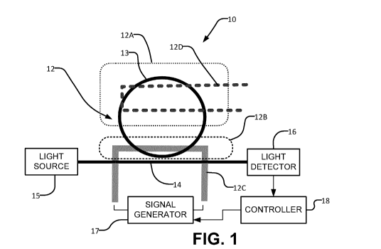
region
12B).
[0177] The phase shift modulator (whether heater 12C or another mechanism) is
controllable to modulate the phase shift provided in phase shift region 12B
over a
range. Preferably the range of modulation of the phase shift provided by phase
shift
region 12B is at least 2-rr radians (which corresponds to the free spectral
range
("FSR") of resonator 12) since this ensures that the range of modulation will
include at
least one instance of any particular peak (e.g. 31A, 31B, 31C, 31D). In some
embodiments the range of the phase shift modulator is sufficient to permit
both small
shifts and shifts of up to several times the FSR.
[0178] Fig. 3 also shows that if the modulation of the phase has a large
enough range
then the same peak 31 may be encountered multiple times with different
instances of
peak 31 separated by phase shifts of 2-rr radians. Fig. 3 shows, for example,
peaks
31A' and 31D' which correspond respectively to peaks 31A and 31D.
[0179] Fig. 4 shows another example apparatus 40 which is similar to apparatus
10
except that waveguide 13 has been replaced with a sub-wavelength light guide
43. A
subwavelength light guide is a waveguide that is divided into small segments
having a
scale substantially smaller than the wavelength of light propagating in the
waveguide
(e.g. substantially smaller than the wavelength of the light emitted by light
source 15).
Sub-wavelength waveguides are described for example in Robert Halir et al.
Waveguide sub-wavelength structures: a review of principles and applications
Laser
Photonics Rev. 9, No. 1, 25-49 (2015) / DOI 10.1002/Ipor.201400083 and in Han
Yun
et al., Broadband 2 x 2 adiabatic 3 dB coupler using silicon-on-insulator sub-
wavelength grating waveguides Optics Letters Vol. 41, Issue 13, pp. 3041-3044
(2016) https://doi.org/10.1364/0L.41.003041.
22
CA 03174690 2022-09-07
WO 2021/207834
PCT/CA2021/050497
[0180] The construction of subwavelength light guide 43 reduces thermal
crosstalk
between the portion of waveguide 43 in region 12B and the portion of waveguide
43
in region 12A. The use of sub-wavelength materials may also increase
sensitivity of
apparatus 40 (e.g. by providing increased surface area for functionalization).
In some
embodiments the sub-wavelength grating waveguide is a "fishbone" type in which
the
small waveguide segments are connected by a narrow spine.
[0181] Fig. 5 shows an example apparatus 50 which is similar to apparatus 10
of Fig.
1 except that heater 12C is shown to be an in-resonator photoconductive heater
(IRPH) 52 and signal generator 17 is replaced with a circuit 57 that is
configured to
drive IRPH 52 and to detect a signal representing optical power measured by
IRPH
52.
[0182] IRPHs are described, for example, in: Hasitha Jayatilleka et al.,
Wavelength
tuning and stabilization of microring-based filters using silicon in-resonator
photoconductive heaters Optics Express Vol. 23, Issue 19, pp. 25084-25097
(2015)
https://doi.org/10.1364/0E.23.02508452. and in Sahba Talebi Fard,et al.
Silicon-on-
insulator sensors using integrated resonance-enhanced defect-mediated
photodetectors Optics Express Vol. 22, Issue 23, pp. 28517-28529 (2014)
https://doi.ord/10.1364/0E.22.028517.
[0183] An IRPH can be applied to act as either or both of a heater and a light
detector. In some embodiments an IPRH is applied as both a heater and a light
detector. An IRPH enables the direct detection of optical power within
resonator 12.
The resonant frequency of resonator 12 may be determined as being at a maximum
of the detected power. Since IRPH 52 can act as an optical detector, an
optical
detector 16 is not required in apparatus 50.
[0184] In any embodiments of the present technology IPRH 52 may be implemented
in various ways. For example, IPRH 52 may be based on any of: a n+, n, n+
device; a
p+, p, p+ device; a p, i, n device; or a reverse-biased PN junction.
Electrical current
flow at the IPRH may be transverse to waveguide 13 but this is not necessary.
An
IPRH may have any other orientation relative to waveguide 13 that is practical
in the
circumstances of a particular embodiment. . Also, while an IPRH device may be
located at a coupling region (e.g. a region where light is coupled between a
waveguide 14 and a resonator 12, this is not mandatory, in any embodiment
described herein an IPRH may have other positions along a resonator 12.
Locating
23
CA 03174690 2022-09-07
WO 2021/207834
PCT/CA2021/050497
and IPRH 52 at or near a coupling region can be convenient for facilitating
physical
separation between phase shift region 12B which may include the IPRH 52 and a
sensing region 12A of the resonator.
[0185] Figure 6 shows example electrical signals measured by IRPH 52 as a
function
of IRPH heater power. The electrical signals represent optical power in
resonator 12
for different concentrations of an analyte.
[0186] In operation, the voltage (or current) supplied to IRPH 52 is
modulated. The
electrical current passing through IRPH 52 causes heating, thereby modulating
the
phase and modulating the resonant frequency of resonator 12. The change in the
current (or voltage) is related to the intensity of the light in resonator 12,
which is
detected by IRPH 52. Thus, IRPH 52 returns an output that may be used as a
proxy
for the optical spectrum, where the independent wavelength variable is
replaced by
the heater power, which is modulated in time.
[0187] Fig. 6 shows four example curves 60. A first curve 60 corresponding to
no
analyte concentration includes peaks 60A and 60A'. Other curves 60
respectively
include peaks 60B, 60C and 60D which respectively correspond to increasing
analyte
concentrations as well as other corresponding peaks at heater power levels
corresponding to phase shifts of multiples of 2-rr.
[0188] Fig. 7 shows example apparatus 70 that is similar to apparatus 50 of
Fig. 5
except that solid core waveguide 13 is replaced by a waveguide 73 that
includes a
sub-wavelength material part 73A and a solid core part 73B. Sub-wavelength
part
73A extends through region 12A and solid core part 73B is provided at least in
the
part of waveguide 73 that includes IRPH 52. Waveguide converters may be
provided
where parts 73A and 73B connect to one another.
[0189] Fig. 7A shows an example transition region 77 which serves as a
waveguide
converter.. Waveguide converters are described for example in: Han Yun et
al.(cited
above). The use of sub-wavelength materials for the part of waveguide 73 that
is in
contact with a fluid to be tested for analyte(s) of interest increases the
sensitivity of
apparatus 70, and provides improved thermal isolation between regions 12A and
12B.
[0190] Fig. 8 shows an example apparatus 80 which is the same as apparatus 70
except that the shape of resonator 12 has been altered so that sub-wavelength
24
CA 03174690 2022-09-07
WO 2021/207834
PCT/CA2021/050497
waveguide part 73A is straight rather than curved. This construction reduces
optical
losses.
[0191] Fig. 9 shows an example apparatus 90 which is similar to apparatus 80
except
that waveguide 73 has been replaced by a waveguide 93 that include low loss
waveguide portions 93A and 93B that connect waveguide portions 73A and 73B.
This
construction can provide increased physical separation between region 12A and
region 12B. Separating region 12A which senses an analyte from region 12B
which is
heated to tune the resonant frequency of resonator 12 has the advantage of
reducing
or eliminating thermal heating of sensing region 12A (thermal crosstalk).
Heater
region 12B can be in a location that is not in proximity to the analyte,
thereby reducing
heating effects on the analyte.
[0192] Fig.9A shows an example layout for a resonator of the general type
illustrated
in Fig. 9 in which a sensing region 12A is separated from a phase modulation
region
12B by a relatively large distance. Low-loss waveguides 93A and 93B connect
parts
of the structure associated with region 12A and parts of the structure in
region 12B
that are associated with phase modulation and light detection.
[0193] The addition of low-loss waveguide portions 93A and 93B may increase
the
total length of resonator 12. This will decrease the free spectral range.
However,
because the quality factor Q is increased while the FSR is simultaneously
decreased,
the net result is that the Finesse remains approximately constant. Therefore,
the
sensitivity may be reduced, but the linewidth of resonator 12 can
correspondingly also
be reduced. This means that the same limit of detection may be achieved, but
with
the advantage of thermal isolation.
[0194] Low-loss waveguide portions 93A, 93B may, for example, be implemented
using a wide waveguide as described for example in Miguel A. Guillen-Torres,
et al.
Effects of backscattering in high-Q, large-area silicon-on-insulator ring
resonators
Optics Letters Vol. 41, Issue 7, pp. 1538-1541 (2016)
https://doi.orq/10.1364/0L.41.001538 and/or by making low loss waveguide
portions
93A, 93B of a low-loss material such as silicon nitride.
[0195] An advantage of including low-loss waveguides in resonator 12 is that
doing
so can increase the quality factor (Q) of resonator 12 as described for
example in
Miguel A. Guillen-Torres, et al. (cited above). If it is desired to increase
the sensitivity
of the apparatus described herein (with "sensitivity" defined as the change in
the
CA 03174690 2022-09-07
WO 2021/207834
PCT/CA2021/050497
resonant wavelength versus the change in concentration of an analyte of
interest) one
can both increase the length of the part of resonator 12 that senses the
analyte of
interest and also increase the quality factor Q of resonator 12, for example
by using
low-loss materials and construction for resonator 12.
[0196] Fig. 10 shows an apparatus 100 that is similar to apparatus 90 except
that
instead of an IRPH it includes a heater external to resonator 12.
[0197] Fig. 11 shows example apparatus 110 that is similar to apparatus 80 of
Fig. 8,
except that apparatus 110 includes a tunable directional optical coupler 119
between
waveguide 14 and resonator 12. Directional coupler 119 may, for example be
based
on a Mach-Zehnder interferometer. Directional coupler 119 may, for example be
thermally adjustable. Directional coupler 119 permits adjustment of the
coupling
coefficient between waveguide 14 and resonator 12. This is especially useful
when
the losses due to fabrication or due to the analyte are unknown a-priori. Such
losses
may be accounted for during the measurement. A variable directional coupler
119
may be used together with other resonators as described herein. For example in
apparatus of the types illustrated in any of Figures 1, 4, 5, 7, 8 or 9.
[0198] Fig. 12 shows example apparatus 120 which is similar to apparatus 40
except
that resonator 12 is replaced with a contra-directional coupler (CDC) 122.
CDCs are
described for example in: Wei Shi, et al. Silicon photonic grating-assisted,
contra-
directional couplers Optics Express Vol. 21, Issue 3, pp. 3633-3650 (2013)
https://doi.org/10.1364/0E.21.003633. CDC 122 incudes first and second
waveguides
123A and 123B optically connected by a grating 123C. In apparatus 120 a shift
in
grating 123C creates a resonator. A portion 12A of the resonator is
functionalized and
exposed to a fluid that may contain an analyte of interest. A separate portion
12B of
the resonator is located to receive heat from a heater 12C.
[0199] As in other embodiments, the intensity of light present in an optical
output
123D, in this case waveguide 123B, has a functional relationship to a
concentration of
an analyte of interest that is captured in portion 12A. Two or more of
apparatus 120
may be cascaded (e.g. connected in series).
[0200] CDC 122 may be made with solid-core waveguides, or sub-wavelength
grating
waveguides.
[0201] Figure 13 schematically illustrates another example apparatus 130 that
is
26
CA 03174690 2022-09-07
WO 2021/207834
PCT/CA2021/050497
operable to detect an analyte of interest. Apparatus 130 is based on an
interferometric principle. Apparatus 130 comprises an interferometer 132 (in
this
example a Mach Zehnder interferometer). Interferometer 132 includes optical
waveguides arranged to provide a sensor branch 132A and a reference branch
132B.
Coherent light incident at an input 133A is split at 134A into branches 132A
and
132B. Light from branches 132A and 132B is recombined at 134B. The recombined
light interferes and is carried to output 133B.
[0202] Sensor branch 132A includes a region 12A in which the waveguide of
sensor
branch 132A is functionalized and exposed to a sample. Reference branch 132B
includes a phase modulation region 12B in which the waveguide of reference
branch
132B is controllably heated by a heater 12C.
[0203] The light output at output 133B depends on the relative optical path
lengths of
sensor branch 132A and reference branch 132B. The optical path length of
sensor
branch 132A is affected by the presence and concentration of an analyte of
interest in
region 12A. The optical path length of reference branch 132B is affected by
the
temperature of the waveguide in region 12B. By varying the temperature in
region
12B using heater 12C one can sweep the optical path length of reference branch
132B such that the variation of light output at 133B with temperature in
region 12B (or
equivalently with the output of heater 12C) provides a signal that contains
information
regarding the presence and concentration of an analyte of interest in region
12A.
[0204] Apparatus 130 may be varied in many ways, for example, by placing phase
modulation region 12B and sample region 12A in the same branch (e.g. a phase
modulation region may be provided at location 12B' in branch 132A. Other
example
variations include different constructions for phase modulation region 12 as
described
herein, different constructions for waveguides etc.. In some embodiments
branches
132A and 132B are routed such that regions 12A and 12B are physically
separated
by a relatively large distance. This may have the effect of reducing thermal
crosstalk
between region 12B and other parts of apparatus 130. For example a heater may
be
placed in a region that is not in proximity to analyte, thereby reducing
heating effects
on the analyte.
[0205] Apparatus according to the present invention may combine plural
sensors.
Different ones of the plural sensors may, for example, may be configured to
detect
different analytes (e.g. by providing different functionalization in region
12A). In some
27
CA 03174690 2022-09-07
WO 2021/207834
PCT/CA2021/050497
embodiments, one or more of the plural sensors is configured to detect
reference
analyte(s) or no analytes at all. Such sensors may be used for calibration of
the
apparatus (e.g. to take account of factors such as ambient temperature,
dilution of
samples, common-mode noise, etc.).
[0206] Figs. 14 and 15 show non-limiting examples of apparatus that includes
plural
resonators 12 (individually identified as 12-1, 12-2 etc.). Such apparatus may
deliver
light to plural resonators 12 from a single light source (e.g. a single
laser). Such
apparatus optionally include a single detector connected to detect output
light
modulated by plural resonators 12.
[0207] Fig. 14 shows example apparatus 140 which comprises a plurality of
cascaded
sensors 141-1 ... 141-N (collectively or generally sensors 141). N may be any
suitable number of sensors 141 such as 2, 3, 4, 10, 20 etc. Fig.14 illustrates
the case
where all of sensors 141 are monitored by a single light detector 16. Sensors
141
may, for example, be of any of the types illustrated in Figs.1, 4, 7, 8, 9, 10
or 11 or
any variation thereof. In apparatus 140 phase modulation for sensors 141 is
provided
by a heater 12C. However, other mechanisms for phase modulation of sensors 141
are also possible.
[0208] Different ones of sensors 141 may be exposed to the same or different
fluids.
For example, in some embodiments, parts 12A of some or all different sensors
141
may be in different chambers which may contain different samples for analysis
and/or
calibration fluids. In some embodiments sensing regions 12A of a group of two
or
more sensors 141 or of all sensors 141 are located in a common chamber that
can
receive a sample for testing (e.g. a blood sample).
[0209] To facilitate separate readout of different sensors 141, sensors 141-1
to 141-N
may be configured to be resonant with the wavelength of light from a light
source 15
at different times. For example, in the absence of phase modulation applied in
region
12B, sensors 141-1 to 141-N may have different resonant wavelengths. This may
be
achieved for example by making resonators 12 of sensors 141-1 to 141-N to have
different dimensions and/or of different materials (e.g. differently doping
the material
of resonators 12). This facilitates use of a single light detector 16 to
detect outputs
from each of sensors 141-1 to 141-N.
[0210] In apparatus 140 sensors 141-1 to 141-N share a single heater 12C that
controls the phase shift applied in regions 12B so that the resonant
wavelengths of
28
CA 03174690 2022-09-07
WO 2021/207834
PCT/CA2021/050497
resonators 12 of sensors 141-1 to 141-N can be controlled to shift
simultaneously my
modulating power delivered by heater 12C. Detector 16 thus measures
simultaneously a proxy to the optical spectra of resonators 12 of each of
sensors 141-
1 to 141-N, where the independent wavelength variable is replaced by the
heater
power, which is modulated in time. The output signal of light detector 16 may
then be
analyzed to determine the shift in the resonant wavelength for each resonator
12,
thereby extracting information about the analytes to which each sensor 141 is
exposed in region 12A.
[0211] In some embodiments, heater 12C is configured to affect different ones
of
sensors 141-1 to 141-N differently, for example the length of a waveguide of
different
resonators 12 that are heated by heater 12C may be different so that for the
same
temperature of heater 12C different phase shifts are applied to different ones
of
resonators 12. This construction may be applied to help separate features
corresponding to resonances of individual sensors 141 in the light detected by
light
detector 16.
[0212] In some embodiments, the phase shifts applied to individual sensors 141
is
individually controllable (e.g. by providing separate phase shifting
mechanisms such
as separate heaters, separate IPRH devices or other suitable phase shifting
mechanisms including those described elsewhere herein). In such embodiments
the
phase shift modulation applied to sensors 141-1 to 141-N may be coordinated to
cause features (e.g. resonant peaks or valleys) in optical output signals of
different
ones of sensors 141-1 to 141-N to be presented at detector 16 at different
times.
[0213] Fig. 15 shows another example apparatus 150 that is similar to
apparatus 140
and includes cascaded sensors 151-1 to 151-N (collectively or generally
sensors
151). Each of sensors 151 may include a resonator according to any of the
examples
described herein and variations thereof that is optically coupled to waveguide
14 that
carries light from a light source 15 as described herein (not shown in Fig.
15). The
light may be supplied at laser input 14A.
[0214] Apparatus 150 differs from apparatus 140 in that heater 12C is replaced
with
individual IPRH 52 (labelled 52-1 to 52-N). Each IPRH 52-1 to 52-N may be
operated
to control the resonant wavelength of the resonator 12 of the corresponding
sensor
151 (e.g. by modulating a phase shift provided by a corresponding one of
regions
12B-1, , 12B-N). Each IPRH 52-1 to 52-N may optionally be operated to read
out
29
CA 03174690 2022-09-07
WO 2021/207834
PCT/CA2021/050497
the corresponding sensor 151.
[0215] In apparatus 140 and apparatus 150 it is desirable that the resonance
frequencies of different ones of resonators 12 be distinct and not spectrally
overlapping, otherwise it tends to become difficult to extract the information
from
individual sensors. This is because when resonant frequencies of different
resonators
12 in apparatus 140 or 150 are too close there will be cross-talk between the
different
sensor readings. The crosstalk arises from a mechanism similar to what happens
in a
ring resonator-based data communication system as described, for example, in
[H.
Jayatilleka et al, Crosstalk in SO! Microring Resonator-Based Filters, IEEE
JLT Vol.
34, Issue 12, pp. 2886-2896 (2016).
[0216] The maximum practical number of sensors in a multiplexed system of the
types illustrated in Figs. 14 and 15 is related to the Finesse of the
resonators, where
Finesse is the ratio of a resonator's free spectral range (FSR) to the
resonator's
optical linewidth.
[0217] In some embodiments that include three or more cascaded sensors,
outputs
from some of the sensors are read out using a combined detector 16 while
outputs of
one or more of the sensors is read out using a separate detector (e.g. a
corresponding IPRH 52). In some embodiments outputs of one or more sensors may
be read out both by a shared detector 16 and a dedicated detector (e.g. an
IPRH 52).
[0218] In some embodiments, a system of multiplexed or cascading sensors as
described herein (e.g. a system as illustrated in Fig. 14 or 15) includes one
or more
tunable couplers (e.g. a tunable coupler 119 as illustrated in Fig. 11) that
optically
couple resonators of different sensors to a waveguide 14 that carries light
from a light
source. A single control input may control coupling to two or more resonators.
For
example, a common heater may control coupling of two or more different
resonators
to a waveguide 14. Providing optical couplers under common control for two or
more
sensors can be particularly useful in the case where each of the sensors are
sensing
analytes from the same source (e.g. the same sample of blood or other fluid).
[0219] Fig. 16 illustrates an example testing apparatus 160. Apparatus 160
comprises
a chip or substrate 161 that accommodates one or more sensors according to any
embodiment described herein. The illustrated embodiment comprises a light
source
15 comprising a laser 165 formed on substrate 161.
CA 03174690 2022-09-07
WO 2021/207834
PCT/CA2021/050497
[0220] An output of laser 15 is optically connected to a waveguide 14. Such
connections may for example be provided by integrated photonic circuits or
using
photonic wirebonding (PWB) techniques. An advantage of integrating laser 15 on
chip
161, either monolithically or attached through techniques such as photonic
wire
bonding advantageously can reduce noise due to mechanical vibration and may
improve the system limit of detection.
[0221] One or more resonators12 (12-1 to 12-4 are shown by way of
illustration) are
formed on substrate 161. Portions of resonators 12 project into a fluid
environment
suitable for bringing a sample and/or calibration fluids and/or
functionalizing agents
into contact with sensing portions of resonators 12. In the illustrated
embodiment the
fluid environment is provided by a microfluidic channel 167 into which a
sample that
may contain one or more analytes maybe delivered. The portions of different
ones of
resonators 12 that project into channel 167 may be functionalized to bind to
or
otherwise interact with corresponding different analytes.
[0222] In some embodiments, apparatus 160 is configured with electrical
contacts to
interface to a control system configured to control and read out sensors of
apparatus
160 as described herein. Apparatus 160 comprise a disposable item. Apparatus
160
may be used for testing fluids such as blood, environmental samples,
industrial
samples etc. Apparatus 160 may have any suitable arrangement of microfluidic
passages 167 to bring samples, calibration fluids or the like to one or more
sensors
on substrate 161 with any desired timing.
[0223] In some embodiments apparatus 160 includes on-board electronics which
may
be integrated into chip 161 and/or packaged in another way (e.g. on a circuit
board or
other electronics platform electrically connected to chip 161). The
electronics may
control operation of the sensors and/or process data from the sensors to
determine
whether certain analyte(s) are present in a sample and if so what are the
concentration(s) of the analyte(s). In some embodiments the onboard
electronics
monitor changes over a time span which permits analysis of kinetics of an
interaction
between an analyte and functionalization on resonators 12 (e.g. kinetics of
binding or
other detection reaction of an analyte to the functionalization of a specific
resonator
12) In some embodiments apparatus 160 includes a wireless data transmitter
operable to transmit data and/or results for a sample to one or more other
devices.
[0224] Fig. 16A is a block and schematic diagram showing another example
31
CA 03174690 2022-09-07
WO 2021/207834
PCT/CA2021/050497
apparatus 160A that includes a laser and plural sensors as described herein
integrated with circuits configured to control the sensors, acquire data from
the
sensors and process the acquired data.
[0225] Apparatus 160A is an example of apparatus which includes two sensors as
described herein. A first sensor 12-1 acts as a sample sensor and is exposed
to a
sample to be analyzed for one or more analytes. A second sensor 12-2 acts as a
reference sensor and is exposed to a reference fluid such as distilled water.
Sensors
12-1 and 12-2 may otherwise be the same. Outputs of sensors 12-1 and 12-2 are
respectively detected by light detectors 16-1 and 16-2. Outputs of light
detectors 16-1
and 16-2 are amplified by a differential trans impedance amplifier and
digitized by an
analog to digital converter. Any type of sensors as described herein may be
used as a
reference sensor and corresponding sample sensor.
[0226] Apparatus 160A includes one or more data processors (Digital Unit)
configured to process the digitized differential output signal.
[0227] Apparatus 160A includes one or more wireless communication transmitters
169 that may be operated to transmit data and/or results obtained by
processing the
data to an external device such as a smart phone 168 or another networked
computing device.
[0228] Sensors as described herein may be calibrated using known
concentrations of
analytes of interest. The timing of detected features in detected light (e.g.
peaks or
valleys) may be measured relative to the phase shift control signal (e.g. an
electrical
current driving a heater 12C). In this manner one can obtain measurements
which
show the timing of the peaks or other features of the detected light for
various
concentrations of the analyte of interest. A calibration function or lookup
table may be
constructed from these values.
[0229] Precise times for the features (peaks) may be determined by fitting a
function
e.g. a Lorentzian lineshape function to the peaks. Shifts in the timing of
peaks may be
correlated to analyte concentraions.
[0230] In some embodiments the timing of readout features (peaks) may be
measured for two or more sensors. For example, an active sensor may be exposed
to
a certain concentration of an analyte of interest and another "calibration"
sensor may
be exposed to a calibration substance such as distilled water. The relative
timing of
32
CA 03174690 2022-09-07
WO 2021/207834
PCT/CA2021/050497
peaks from the two sensors may be measured and used for calibration. Using the
relative timing of an active sensor and a calibration sensor may be
advantageous
since changes in factors such as ambient temperature, heater sweep rate, etc.
may
affect both the active sensor and the calibration sensor equally such that
measurements based on that relative timing may be relatively insensitive to
such
changes.
[0231] In some embodiments calibration information such as a calibration
function or
lookup table are stored in a data store accessible to a controller as
described herein.
Such data may for example be stored in a data store on substrate 161 of
apparatus
160.
[0232] In some embodiments apparatus as described herein may be applied to
obtain
"sensorgrams" which measure dynamic changes in sensor readouts as the sensors
are exposed to an analyte. A sensorgram may be obtained by measuring
variations in
the timing of a peak from a sensor at various times after a sample has been
applied
to the sensor.
[0233] In some embodiments outputs from one or more sensors as described
herein
may be input to an artificial intelligence such as a neural network (NN) that
has been
trained to associate patterns (e.g. sensorgrams, comparisons of output signals
from
different sensors etc.) in the sensor outputs with different analytes of
interest and/or
different concentrations of analytes of interest. This may help to rapidly or
accurately
(or both) determine whether a particular analyte of interest is present or not
present.
Use of a trained NN may also help to process data from multiple sensors that
are
configured to detect multiple different analytes of interest.
[0234] Various optical detection schemes may optionally be applied to improve
the
accuracy of apparatus as described herein. Some examples of such schemes are
described below. Figs. 17A and 17B show example apparatus 170 that is similar
to
apparatus 10 of Fig. 1 with the addition of a readout system 171 and an
optical switch
in Fig. 17B. The optical switch may, for example, be implemented by a Mach-
Zehnder
interferometer, ring resonator, etc. Fig. 17B shows an implementation with a
switch
175 based on a Mach-Zehnder interferometer configuration. Readout system 171
may also be used in combination with other apparatus as described herein.
[0235] Readout system 171 functions in a manner similar to a lock-in
amplifier. A
periodic signal Vch1(t) is applied to drive a heater (e.g. heater 12C) in a
portion of the
33
CA 03174690 2022-09-07
WO 2021/207834
PCT/CA2021/050497
sensor (Fig. 17A) or in an optical switch 175 after the sensor (Fig. 17B). A
lock-in
signal Vch2(t) is derived from Vch1(t). The lock-in signal Vch2(t) has a set
phase
relationship to Vch1(t) (Fig. 17A) or is the same as Vch1(t) (Fig. 17B). Lock-
in signal
Vch2(t) may, for example be a train of short square pulses. The lock-in signal
Vch2(t)
is then applied together with the output signal from the light detector 16 to
a mixing
circuit 174 whose output is integrated over a plurality of (in some
embodiments a
large number of) cycles of Vch1(t). This reduces the noise due to mechanical
vibrations, electronic circuits, etc.
[0236] This may be repeated with different phase relationships of Vch2(t) to
Vch1(t) to
obtain integrated output values corresponding to different phase shifts. The
resulting
outputs may be processed to detect peaks corresponding to the presence of an
analyte at a particular concentration level.
[0237] In the embodiments illustrated in Fig. 17A and 17B, light output from
the
sensor is detected at photodetector 16. An electrical current signal output by
photodetector 16 is converted to a voltage signal by transimpedance amplifier
173.
The voltage signal output by transimpedance amplifier 173 is combined at mixer
174
with signal Vch2(t).
[0238] Some embodiments apply coherent light detection. Coherent light
detection
can detect both phase of detected light relative to a reference phase and
amplitude of
the detected light. Detecting both phase and amplitude (coherent detection)
can
reduce or eliminate the sensitivity fading and directional ambiguity issues
that are
typically associated with readouts of interferometric sensors. Coherent
detectors are
described, for example in I. Molina-Fernandez et al, Fundamental limit of
detection of
photonic biosensors with coherent phase read-out, Optics express, vol. 27, no.
9, Apr.
2019, 12616-12629.
[0239] Coherent light detection typically does not perform well for detecting
output of
sensors which include ring resonators driven by fixed wavelength light unless
the ring
resonator is close to being resonant with the fixed wavelength light and the
coupling
between the ring resonator and the waveguide that provides the light is close
to
critical coupling.
[0240] Fig. 18 shows an example apparatus 180 which implements an example
coherent detection arrangement. In apparatus 180, light from laser light
source 15 is
split into a reference beam carried by reference waveguide 181 and a sensor
beam
34
CA 03174690 2022-09-07
WO 2021/207834
PCT/CA2021/050497
carried by sensor waveguide 184. Sensor waveguide 184 is optically coupled to
a ring
resonator 12 (which may be configured according to any embodiment described
herein).
[0241] Both reference waveguide 181 and sensor waveguide 184 deliver light to
a
coherent detector 185. To improve performance of coherent detector 185, a
phase
shift mechanism is used to bring the resonant frequency of resonator 12 close
to the
frequency of the light from laser light source 15. This may be achieved, for
example,
by applying a constant bias current to a heater that heats the material of a
part of a
waveguide of ring resonator 12. In some embodiments the same heater 12C is
used
to modulate (e.g. sweep) the phase shift applied in portion 12B of resonator
12 to an
optimum phase shift selected to adjust the resonant frequency of ring
resonator 12
relative to the frequency of the light supplied by laser light source 15 for
proper
functioning of coherent detector 185.
[0242] A tunable coupler 119 (see e.g. Fig.11) may optionally be provided in
apparatus 180 to adjust optical coupling of ring resonator 12 to sensor
waveguide 181
for optimal performance of coherent detector 185.
[0243] Apparatus that employs coherent detection (e.g. apparatus like
apparatus 180
of Fig. 18 optionally includes noise reduction circuitry similar to that shown
in Fig. 17.
[0244] Fig. 19 shows an example apparatus 190 that includes a phase shift
mechanism that is configured to vary a phase shift applied to signal waveguide
191
according to a signal Vch1(t). Signal Vch1(t) may, for example, control or
correspond
to a signal driving a heater. A lock-in signal Vch2(t) is derived from signal
Vch1(t).
[0245] Coherent detector 195 is like coherent detector 185 with the addition
of mixers
1901 and 190Q. Lock-in signal Vch2(t) is mixed with inphase and quadrature
signals
at mixers 1901 and 190Q respectively.
[0246] Fig 20 shows example apparatus 200 that has a coherent detector 195
like
that of apparatus 190 except the sensor has a configuration like that of
apparatus 180
(Fig. 18). Signal Vch1(t) may, for example, control or correspond to a signal
driving a
heater at the waveguide 191 or 194. A lock-in signal Vch2(t) is derived from
signal
Vch1(t).
[0247] In some embodiments apparatus as described herein comprises one or more
additional heaters. The additional heaters may include a sensor heater that is
located
CA 03174690 2022-09-07
WO 2021/207834
PCT/CA2021/050497
and controllable to selectively heat sensor region 12A and/or a sample heater
disposed to selectively heat a sample being introduced into the sensor region
of
apparatus as described herein. The additional heater(s) may, for example
comprise a
resistive heater comprising a metallic material or doped semiconductor through
which
an electrical current can be passed to heat the sensor region. An example
additional
heater 12D is schematically illustrated in Fig. 1. Any other embodiment as
described
herein may include one or more additional heaters. Additional heaters may be
integrated within sensing region 12A or elsewhere in a fluid path by way of
which
samples and or reference fluids are delivered to sensing region 12A.i
[0248] Local heating of the waveguide surface or sample may be used to monitor
the
thermal stability of functionalized waveguide surfaces (e.g., assessing the
thermal
stability of new or existing specific detection receptors such as antibodies
and/or
aptamers). For example an additional heater 12D may be operated to raise a
temperature of a functionalized waveguide to a temperature in the range of
about.,
20-90 C. At a temperature of interest, instability of functionalized surfaces
of
waveguide 13 may be detected by analysis of resonance peak shifts indicative
of
removal/desorption of the functionalization chemistry, or change/denaturation
of the
functionalization chemistry, either of which may result in a refractive index
change
(e.g., removal of antibody or aptamer from the waveguide surface would result
in a
negative peak shift by decreasing the effective refractive index).
[0249] Instability of functionalization of waveguide 13 or temperature
dependent
behavior of one or more analytes in a sample may also be assessed as a
function of
temperature. This may be done, for example by monitoring a difference in
output of a
sensor as described herein connected to receive a sample in sensor region 12B
and
another sensor, preferably of the same type that has a reference fluid (e.g.
distilled
water, a buffer or the like) in sensor region 12B. Operating conditions of
both the
sample sensor and the reference sensor may be kept the same. Data from the
sample and reference sensors may be processed to assess stability of the
functionalization of waveguide 13.
[0250] Local heating may also be applied to analyze molecular conformation or
other
properties of biological molecules in a sample (e.g., through DNA or aptamer
melting
curve analysis). For example heat induced changes in an analyte of interest
(e.g.
"melting") may be monitored by varying (e.g. sweeping) a temperature of sensor
36
CA 03174690 2022-09-07
WO 2021/207834
PCT/CA2021/050497
region 12A. For example, temperatures in the range of about 40, 50 or 60 C to
about
98 C may be used to obtain additional information about analytes that are
biological
molecules. Specific temperature ranges may be selected for the specific
analyte(s) of
interest. In such applications, melting temperatures (e.g., of DNA or aptamer)
may be
assessed by monitoring changes in resonance peak shifts (which can result from
changes in the effective refractive index of waveguide 13 introduced by
melting of an
analyte that is bound to or otherwise interacting with waveguide 13). Melting
temperature analysis can aid understanding of the structure and stability of
the
analyte(s) of interest.
[0251] Principles of melting temperature analysis are described, for example
in: Luo
et al. Developing a combined strategy for monitoring the progress of aptamer
selection. Analyst, 2017, 142, 3136; and Ririe, Rasmussen, and Wittwer.
Product
Differentiation by Analysis of DNA Melting Curves during the Polymerase Chain
Reaction. Analytical Biochemistry, 1997, 245, 154-160.
[0252] Sample heating may also be beneficial in characterizing temperature-
dependent reactions of an analyte of interest.
[0253] In applications where the temperature of sensing region 12B is varied
(e.g. by
sweeping) it can be necessary to separate the effects on the optical output of
a
sensor (any sensor as described herein) which result from changes in the
functionalization chemistry and/or the analyte of interest or the interaction
of the
functionalization chemistry and/or the analyte of interest with the waveguide
from
other effects on the optical output of the sensor that result from the change
of
temperature of the waveguide. Various approaches may be taken to provide such
correction or compensation.
[0254] One approach is to use the combination of a reference sensor with a
sample
sensor as described above. The differential output of the reference and sample
sensors may be monitored and processed.
[0255] Another approach operates a phase shift modulator (e.g., heater),
external to
sensing region 12B (e.g. a heater 12C or equivalently an IPRH) to isolate
surface/sample-induced effects on the resonance of a resonator from resonance
changes which arise from the changes of temperature of the waveguide in
sensing
region 12B. With this approach, the phase shift modulator external to sensing
region
12B may be operated to compensate for phase shift arising from heating within
37
CA 03174690 2022-09-07
WO 2021/207834
PCT/CA2021/050497
sensing region 12B.
[0256] Another approach applies multi-dimensional calibration information
which
includes temperature of sensing region 12B to correct for any effect of the
heating of
sensing region 12B on the resonant behavior of a resonator 12. Such
calibration
information may be provided in a calibration function or lookup table and/or
may be
embodied in a trained neural network which takes a temperature of sensing
region
12A or a surrogate for the temperature of sensor region 12A (e.g. a heater
control
current or other heater control signal) as one input together with other data
to be
processed (e.g readings from one or more light detectors.
Interpretation of Terms
[0257] Unless the context clearly requires otherwise, throughout the
description and
the claims:
= "comprise", "comprising", and the like are to be construed in an
inclusive
sense, as opposed to an exclusive or exhaustive sense; that is to say, in the
sense of "including, but not limited to";
= "connected", "coupled", or any variant thereof, means any connection or
coupling, either direct or indirect, between two or more elements; the
coupling
or connection between the elements can be physical, logical, or a combination
thereof;
= "herein", "above", "below", and words of similar import, when used to
describe
this specification, shall refer to this specification as a whole, and not to
any
particular portions of this specification;
= "or", in reference to a list of two or more items, covers all of the
following
interpretations of the word: any of the items in the list, all of the items in
the
list, and any combination of the items in the list;
= the singular forms "a", "an", and "the" also include the meaning of any
appropriate plural forms.
[0258] Words that indicate directions such as "vertical", "transverse",
"horizontal",
"upward", "downward", "forward", "backward", "inward", "outward", "left",
"right", "front",
"back", "top", "bottom", "below", "above", "under", and the like, used in this
description
and any accompanying claims (where present), depend on the specific
orientation of
the apparatus described and illustrated. The subject matter described herein
may
assume various alternative orientations. Accordingly, these directional terms
are not
38
CA 03174690 2022-09-07
WO 2021/207834
PCT/CA2021/050497
strictly defined and should not be interpreted narrowly.
[0259] Controllers for example embodiments of the invention may be implemented
using specifically designed hardware, configurable hardware, programmable data
processors configured by the provision of software (which may optionally
comprise
"firmware") capable of executing on the data processors, special purpose
computers
or data processors that are specifically programmed, configured, or
constructed to
perform one or more steps in a method as explained in detail herein and/or
combinations of two or more of these. Examples of specifically designed
hardware
are: logic circuits, application-specific integrated circuits ("ASICs"), large
scale
integrated circuits ("LSIs"), very large scale integrated circuits ("VLSIs"),
and the like.
Examples of configurable hardware are: one or more programmable logic devices
such as programmable array logic ("PALs"), programmable logic arrays ("PLAs"),
and
field programmable gate arrays ("FPGAs"). Examples of programmable data
processors are: microprocessors, digital signal processors ("DSPs"), embedded
processors, graphics processors, math co-processors, general purpose
computers,
server computers, cloud computers, mainframe computers, computer workstations,
and the like. For example, one or more data processors in a control circuit
for a
device may implement methods as described herein by executing software
instructions in a program memory accessible to the processors.
[0260] Where a component (e.g. a light source, waveguide, software module,
light
detector, processor, assembly, device, circuit, etc.) is referred to above,
unless
otherwise indicated, reference to that component (including a reference to a
"means")
should be interpreted as including as equivalents of that component any
component
which performs the function of the described component (i.e., that is
functionally
equivalent), including components which are not structurally equivalent to the
disclosed structure which performs the function in the illustrated exemplary
embodiments of the invention.
[0261] Specific examples of systems, methods and apparatus have been described
herein for purposes of illustration. These are only examples. The technology
provided
herein can be applied to systems other than the example systems described
above.
Many alterations, modifications, additions, omissions, and permutations are
possible
within the practice of this invention. This invention includes variations on
described
embodiments that would be apparent to the skilled addressee, including
variations
39
CA 03174690 2022-09-07
WO 2021/207834
PCT/CA2021/050497
obtained by: replacing features, elements and/or acts with equivalent
features,
elements and/or acts; mixing and matching of features, elements and/or acts
from
different embodiments; combining features, elements and/or acts from
embodiments
as described herein with features, elements and/or acts of other technology;
and/or
omitting combining features, elements and/or acts from described embodiments.
[0262] Various features are described herein as being present in "some
embodiments". Such features are not mandatory and may not be present in all
embodiments. Embodiments of the invention may include zero, any one or any
combination of two or more of such features. All possible combinations of such
features are contemplated by this disclosure even where such features are
shown in
different drawings and/or described in different sections or paragraphs. This
is limited
only to the extent that certain ones of such features are incompatible with
other ones
of such features in the sense that it would be impossible for a person of
ordinary skill
in the art to construct a practical embodiment that combines such incompatible
features. Consequently, the description that "some embodiments" possess
feature A
and "some embodiments" possess feature B should be interpreted as an express
indication that the inventors also contemplate embodiments which combine
features
A and B (unless the description states otherwise or features A and B are
fundamentally incompatible).
[0263] It is therefore intended that the following appended claims and claims
hereafter introduced are interpreted to include all such modifications,
permutations,
additions, omissions, and sub-combinations as may reasonably be inferred. The
scope of the claims should not be limited by the preferred embodiments set
forth in
the examples, but should be given the broadest interpretation consistent with
the
description as a whole.