Note: Descriptions are shown in the official language in which they were submitted.
Attorney Docket 50760-0016CA1
POLARIZATION-DIVERSITY OPTICAL POWER SUPPLY
CROSS-REFERENCE TO RELATED APPLICATION
111 This application claims priority to U.S. provisional patent
application 63/245,011, filed
on September 16, 2021.
BACKGROUND
Field
[2] Various example embodiments relate to optical communication equipment
and, more
specifically but not exclusively, to optical power supplies.
Description of the Related Art
[3] This section introduces aspects that may help facilitate a better
understanding of the
disclosure. Accordingly, the statements of this section are to be read in this
light and are not
to be understood as admissions about what is in the prior art or what is not
in the prior art.
[4] As the input/output (I/0) capacities of electronic processing chips
increase, electrical
signals may not provide sufficient I/O capacity across the limited size of a
practically viable
electronic chip package. A feasible alternative may be to interconnect
electronic chip
packages using optical signals, which can typically be delivered with a much
higher I/O
capacity per unit area compared to electrical I/0s.
SUMMARY OF THE INVENTION
151 Disclosed herein are various embodiments of an optical communication
system including
an optical power supply that has an eye-safety feature. In some examples, the
optical power
supply transmits light (e.g., laser light) to one or more transponder modules
through one or
more optical fibers. Each of the transponder modules reflect or redirect a
portion of the light
back to the optical power supply through the corresponding optical fiber. The
optical power
supply measures the reflected or redirected light from the optical fiber to
evaluate a condition
1
Date Recue/Date Received 2022-09-16
Attorney Docket 50760-0016CA1
of the optical fiber, such as whether the optical fiber is intact or broken.
The optical power
supply reduces the power level of, or shuts off, the light transmitted to the
optical fiber in
response to a determination that the optical fiber is likely broken. This
prevents high power
light from emitting out of a broken end of the optical fiber, thereby reducing
the risk to a
human operator of the optical communication system.
[6] In an apparatus that includes an optical power supply, a power supply
light source
configured to generate power supply light, at least one optical input/output
port, at least one
photodetector, and a coupling module configured to receive the power supply
light from the
power supply light source and output the power supply light through the
optical input/output
port, receive reflected light through the optical input/output port, and
transmit the reflected
light to the photodetector. The apparatus includes the photodetector that is
configured to detect
the reflected light and generate a signal representing a level of the
reflected light, and a
controller that is configured to compare the level of the detected reflected
light with a
threshold value, and upon determining that the level of the detected reflected
light is less than
the threshold value, reduce or turn off the power supply light that is
provided to the optical
input/output port.
[7] In some implementations, the apparatus includes the reflected light that
includes a portion
of the power supply light that is output from the optical input/output port
and reflected back to
the optical input/output port. The controller of the apparatus is configured
to control the light
source to reduce or turn off the power supply light generated by the light
source upon
determining that the level of the detected reflected light is less than the
threshold value. In
some implementations, the controller is configured to control an optical
shutter or attenuator
to reduce or block the power supply light that is provided to the optical
input/output port.
[8] In some implementations, the apparatus includes a transponder module that
that includes a
reflector and a data modulator, in which the reflector is configured to
receive the power supply
light, transmit a first portion of the power supply light to the data
modulator, and reflect a
second portion of the power supply light back to the optical power supply. The
data
2
Date Recue/Date Received 2022-09-16
Attorney Docket 50760-0016CA1
modulator is configured to modulate the first portion of the power supply
light according to
electrical data and generate a modulated optical signal.
[9] In some implementations, the apparatus includes an optical fiber optically
coupled
between the optical power supply and the transponder module, in which the
reflector is
configured to receive the power supply light from the optical fiber and
reflect the second
portion of the power supply light back to the optical power supply through the
optical fiber. In
some implementations, the optical fiber that includes a plurality of segments
of optical fibers
that are optically coupled by connectors, slices, and optical elements, and
the threshold value
is selected to be higher than a sum of all reflected light that is reflected
back to the optical
power supply by the connectors, splices, and optical elements and reflected
light due to the
Fresnel reflection from a broken optical fiber, when the power supply light
source outputs the
power supply light at a normal operation level. In some implementations, the
normal
operational level is inferred from a measurement of a portion of the power
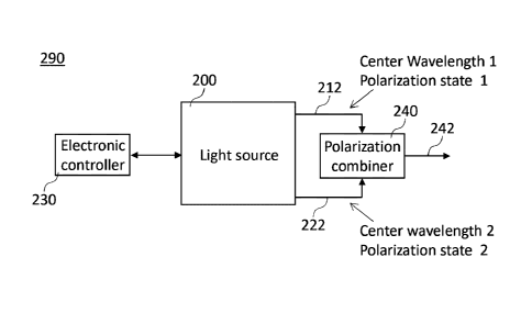
supply light that is
output from the optical input/output port using a second photodetector.
[10] In some implementations, the apparatus includes the optical shutter or
attenuator
positioned between the power supply light source and the coupling module,
wherein the
controller is configured to control the optical shutter or attenuator to
selectively operate in a
first state that allows the power supply light to pass to the coupling module,
or in a second
state that blocks or reduces the power supply light that is provided to the
coupling module.
1111 In some implementations, the apparatus includes a monitor light source
that is
configured to generate monitor light, in which the coupling module is
configured to combine
the power supply light and the monitor light to generate combined light, and
provide the
combined light to the optical input/output port. The reflected light includes
reflected monitor
light, and the coupling module is configured to direct the reflected monitor
light to the
photodetector. The coupling module includes a wavelength
multiplexer/demultiplexer that is
configured to receive the power supply light and the monitor light, combine
the power supply
light and the monitor light to generate the combined light, and provide the
combined light to
the optical input/output port.
3
Date Recue/Date Received 2022-09-16
Attorney Docket 50760-0016CA1
[12] In some implementations, the power supply light of the apparatus has a
first set of one
or more discrete wavelengths or wavelength ranges, the monitor light has a
second set of one
or more discrete wavelengths or wavelength ranges, and at least 10% of optical
power in the
power supply light and at least 10% of optical power in the monitor light are
contained in
disjoint frequency bands. In some implementations, at least 50% of optical
power in the power
supply light and at least 50% of optical power in the monitor light are
contained in disjoint
frequency bands. In some implementations, at least 90% of optical power in the
power supply
light and at least 90% of optical power in the monitor light are contained in
disjoint frequency
bands.
[13] In some implementations, the coupling module of the apparatus includes an
optical
circulator that is positioned between the monitor light source and the
wavelength
multiplexer/demultiplexer, The optical circulator includes a first port, a
second port, and a
third port. The first port is optically coupled to the monitor light source,
the second port is
optically coupled to the wavelength multiplexer/demultiplexer, and the third
port is optically
coupled to the photodetector. The optical circulator is configured to receive
the monitor light
at the first port and output the monitor light at the second port. The optical
circulator is
configured to receive the reflected light at the second port and output the
reflected light at the
third port.
[14] In some implementations, the coupling module of the apparatus includes an
optical
circulator that is positioned between the monitor light source and the
wavelength
multiplexer/demultiplexer. The optical circulator is configured to direct the
monitor light from
the monitor light source to the wavelength multiplexer/demultiplexer, and the
optical
circulator is configured to direct the reflected light to the photodetector.
In some
implementations, the coupling module includes an optical circulator that is
positioned between
the wavelength multiplexer/demultiplexer and the optical input/output port.
The optical
circulator that includes a first port, a second port, and a third port. The
first port is optically
coupled to the wavelength multiplexer/demultiplexer, the second port is
optically coupled to
the optical input/output port, and the third port is optically coupled to the
photodetector. The
optical circulator is configured to receive the combined light at the first
port and output the
4
Date Recue/Date Received 2022-09-16
Attorney Docket 50760-0016CA1
combined light at the second port. The optical circulator is configured to
receive the reflected
light at the second port and output the reflected light at the third port.
[15] In some implementations, the coupling module of the apparatus includes an
optical
circulator that is positioned between the wavelength multiplexer/demultiplexer
and the optical
input/output port. The optical circulator is configured to direct the light
from the wavelength
multiplexer/demultiplexer to the optical input/output port. The optical
circulator is configured
to direct the reflected light to the photodetector.
[16] In some implementations, the coupling module of the apparatus includes an
optical
splitter and an optical circulator. The optical circulator is positioned
between the monitor light
source and the optical splitter. The optical circulator is configured to
direct the monitor light
from the monitor light source to the optical splitter. The optical splitter
includes a first port
and a second port. The optical splitter is configured to split the power
supply light into a first
portion and a second portion, split the monitor light into a first portion and
a second portion,
send the first portion of the power supply light and the first portion of the
monitor light to the
first port of the optical splitter, and send the second portion of the power
supply light and the
second portion of the monitor light to the second port of the optical
splitter.
[17] In some implementations, the optical splitter of the apparatus is
configured to split first
reflected light from the first port of the optical splitter into a first
portion and a second portion,
split second reflected light from the second port of the optical splitter into
a first portion and a
second portion, send the first portion of the first reflected light and the
first portion of the
second reflected light to the optical circulator. The optical circulator is
configured to send the
reflected light from the optical splitter to the photodetector.
[18] In some implementations, the coupling module of the apparatus includes an
optical
splitter and an optical circulator. The optical splitter includes a first port
and a second port.
The optical splitter and the optical circulator are configured to provide a
first portion of power
supply light and a first portion of monitor light to the first port of the
optical splitter, and
provide a second portion of power supply light and a second portion of monitor
light to the
second port of the optical splitter. The optical splitter and the optical
circulator are configured
Date Recue/Date Received 2022-09-16
Attorney Docket 50760-0016CA1
to provide at least a portion of reflected light received at the first port of
the optical splitter and
at least a portion of reflected light received at the second port of the
optical splitter to the
photodetector.
[19] In some implementations, the optical power supply of the apparatus is
configured to
monitor conditions of a first optical fiber optically coupled to the first
port of the optical
splitter and a second optical fiber optically coupled to the second port of
the optical splitter. In
some implementations, the optical power supply is configured to reduce or shut
off the power
supply light provided to the first and second optical fibers upon determining
that the level of
the reflected light detected by the photodetector is less than the threshold
value.
[20] In some implementations, the coupling module of the apparatus includes a
narrow band
optical filter positioned between the optical circulator and the
photodetector, the narrow band
optical filter is configured to allow a larger percentage of the monitor light
to pass and a
smaller percentage of the power supply light to pass.
[21] In some implementations, the apparatus includes at least one optical
input/output port
includes a first optical input/output port and a second optical input/output
port. The at least
one photodetector includes a first photodetector and a second photodetector.
The coupling
module includes an optical splitter, a first optical circulator, and a second
optical circulator.
The optical splitter includes a first output and a second output. The first
optical circulator is
configured to direct light from the first output of the optical splitter to
the first optical
input/output port, and direct reflected light from the first optical
input/output port to the first
photodetector. The second optical circulator is configured to direct light
from the second
output of the optical splitter to the second optical input/output port, and
direct reflected light
from the second optical input/output port to the second photodetector.
[22] In some implementations, the apparatus includes the first optical
circulator is
positioned between the first output of the optical splitter and the first
optical input/output port.
The second optical circulator is positioned between the second output of the
optical splitter
and the second optical input/output port. The first optical circulator
includes a first port, a
second port, and a third port, the first port is optically coupled to the
first output of the optical
6
Date Recue/Date Received 2022-09-16
Attorney Docket 50760-0016CA1
splitter, the second port is optically coupled to the first optical
input/output port, and the third
port is optically coupled to the first photodetector. The second optical
circulator includes a
first port, a second port, and a third port, the first port is optically
coupled to the second output
of the optical splitter, the second port is optically coupled to the second
optical input/output
port, and the third port is optically coupled to the second photodetector.
[23] In some implementations, the optical splitter of the apparatus is
configured to split the
power supply light into a first portion and a second portion, split the
monitor light into a first
portion and a second portion, send the first portion of the power supply light
and the first
portion of the monitor light to the first port of the optical splitter, and
send the second portion
of the power supply light and the second portion of the monitor light to the
second port of the
optical splitter. The first optical circulator is configured to receive the
first portion of the
power supply light and the first portion of the monitor light at the first
port, and output the first
portion of the power supply light and the first portion of the monitor light
at the second port.
The second optical circulator is configured to receive the second portion of
the power supply
light and the second portion of the monitor light at the first port, and
output the second portion
of the power supply light and the second portion of the monitor light at the
second port. The
first optical circulator is configured to receive, at the second port,
reflected light from the first
input/output port, and output the reflected light at the third port, and the
second optical
circulator is configured to receive, at the second port, reflected light from
the second
input/output port, and output the reflected light at the third port.
[24] In some implementations, the coupling module of the apparatus is
configured to
provide the combined light to two or more optical fibers, receive reflected
monitor light from
the two or more optical fibers, and transmit the reflected monitor light from
each optical fiber
to a corresponding photodetector. The reflected monitor light from different
optical fibers are
detected by different photodetectors to enable each optical fiber to be
monitored individually.
[25] In an aspect, the apparatus includes a transponder module that includes a
selective
reflector and a data modulator, in which the selective reflector is configured
to receive the
combined light, transmit the power supply light to the data modulator, and
reflect the monitor
7
Date Recue/Date Received 2022-09-16
Attorney Docket 50760-0016CA1
light back to the optical power supply. The data modulator is configured to
modulate the
power supply light according to electrical data and generate a modulated
optical signal.
[26] In some implementations, the apparatus includes an optical fiber
optically coupled
between the optical power supply and the transponder module, in which the
selective reflector
is configured to receive the combined light from the optical fiber and reflect
the monitor light
back to the optical power supply through the optical fiber.
[27] In some implementations, the coupling module of the apparatus includes an
optical
circulator having a first port, a second port, and a third port. The optical
circulator is
configured to receive the power supply light at the first port and transmit
the power supply
light from the second port to the optical input/output port. The optical
circulator is configured
to receive reflected power supply light at the second port and transmit the
reflected power
supply light from the third port to the photodetector.
[28] In some implementations, the coupling module of the apparatus includes an
optical
splitter having a first port, a second port, a third port, and a fourth port.
The optical splitter is
configured to receive the power supply light at the first port, transmit a
first portion of the
power supply light out of the third port, transmit a second portion of the
power supply light
out of the fourth port, receive first reflected power supply light at the
third port, receive
second reflected power supply light at the fourth port, and transmit a portion
of the first
reflected power supply light and a portion of the second reflected power
supply light out of the
second port to the photodetector.
[29] In some implementations, the optical splitter of the apparatus includes
an optical 50/50
splitter. The coupling module includes an optical splitter having a first
port, a second port, and
a third port. The optical splitter is configured to receive the power supply
light at the first port,
transmit a first portion of the power supply light out of the third port,
receive first reflected
power supply light at the third port, and transmit a portion of the first
reflected power supply
light out of the second port to the photodetector.
8
Date Recue/Date Received 2022-09-16
Attorney Docket 50760-0016CA1
[30] In some implementations, the optical splitter of the apparatus includes
an optical a/(1-
a) splitter, 0 < a <1, and a 0.5. The optical splitter of the apparatus
transmits power supply
light having a power a-P out of the third port, receives reflected power
supply light having a
power PR at the third port, and transmits a portion of the reflected power
supply light having a
power (1-a)-PR out of the second port to the photodetector.
[31] In some implementations, the apparatus includes a transponder module
configured to
receive the power supply light, with or without monitor light, from the
optical power supply
through a first optical fiber, in which the transponder module includes a data
modulator and
mechanism for reflecting a portion of the power supply light or the monitor
light received
from the first optical fiber, either modulated or not modulated, back to the
first optical fiber.
The data modulator is configured to modulate at least a portion of the power
supply light
based on electrical data to generate a modulated optical signal.
[32] In some implementations, the power supply light of the apparatus includes
continuous-
wave light. The power supply light includes one or more trains of periodic
optical pulses. In
some implementations, the power supply light includes one or more trains of
non-periodic
optical pulses. The power supply light includes a sequence of optical frame
templates.
[33] In an aspect, an apparatus includes a transponder module configured to
receive
combined light includes power supply light and monitor light from a first
optical fiber, at least
10% of optical power in the power supply light and at least 10% of optical
power in the
monitor light are contained in disjoint frequency bands. The transponder
module includes a
selective reflector and a data modulator. The selective reflector is
configured to receive the
combined light from the first optical fiber, transmit the power supply light
to the data
modulator, and reflect the monitor light back to the first optical fiber. The
data modulator is
configured to modulate the power supply light based on electrical data to
generate a
modulated optical signal. The selective reflector includes a wavelength
selective
multiplexer/demultiplexer and a minor. The wavelength selective
multiplexer/demultiplexer
includes a first port, a second port, and a third port, the first port is
configured to receive the
combined light from the first optical fiber, the second port is configured to
output the power
9
Date Recue/Date Received 2022-09-16
Attorney Docket 50760-0016CA1
supply light to the data modulator, and the third port is configured to output
the monitor light
to the minor and receive reflected monitor light from the mirror. The
wavelength selective
multiplexer/demultiplexer is configured to transmit the reflected monitor
light back to the first
optical fiber. The selective reflector includes a thin film filter configured
to receive the
combined light from the first optical fiber, transmit the power supply light
to the data
modulator, and reflect the monitor light back to reflected monitor light back
to the first optical
fiber.
[34] In an aspect, an apparatus includes a transponder module configured to
receive power
supply light, with or without additional monitor light, from a first optical
fiber, in which the
transponder module includes a data modulator and a reflecting/redirecting
module. The
reflecting/redirecting module is configured to reflect or redirect a first
portion of the light
received from the first optical fiber, either with or without modulation, back
to the first optical
fiber, the first portion of the light having a power level greater than a
power level of reflected
light caused by a breakage in the first optical fiber. The data modulator is
configured to
modulate at least a portion of the power supply light based on electrical data
to generate a
modulated optical signal. In some implementations, the transponder module is
configured to
receive the power supply light without the additional monitor light, and the
reflecting/redirecting module is configured to reflect or redirect a portion
of the power supply
light back to the first optical fiber. The transponder module includes an
optical circulator and a
data modulator. The data modulator includes an input port, a first output
port, and a second
output port. The optical circulator is configured to receive the power supply
light from the first
optical fiber, transmit the power supply light to the data modulator. In some
implementations,
the data modulator is configured to modulate the power supply light according
to electrical
data and generate a first modulated optical signal and a second modulated
optical signal, and
send the second modulated optical signal to the optical circulator. The
optical circulator is
configured to send the second modulated optical signal to the first optical
fiber.In some
implementations, the data modulator has a Mach-Zehnder interferometer
configuration.
[35] In some implementations, the transponder module of the apparatus includes
a data
modulator, the data modulator includes a first port and a second port, the
data modulator is
Date Recue/Date Received 2022-09-16
Attorney Docket 50760-0016CA1
configured to modulate the power supply light according to electrical data and
generate a first
modulated optical signal and a second modulated optical signal. The data
modulator is
configured to send the second modulated optical signal to the first optical
fiber. In some
implementations, the data modulator has a reflective Mach-Zehnder
interferometer
configuration. The reflecting/redirecting module is configured to receive the
power supply
light with the additional monitor light, and reflect or redirect at least a
portion of the monitor
light back to the first optical fiber.
[36] In an aspect, an apparatus includes a transponder module configured to
receive power
supply light from a first optical fiber, in which the transponder module
includes a partially
reflective device and a data modulator. The partially reflective device is
configured to receive
the power supply light from the first optical fiber, transmit a first portion
of the power supply
light to the data modulator, and reflect a second portion of the power supply
light back to the
first optical fiber. The data modulator is configured to modulate the power
supply light based
on electrical data to generate a modulated optical signal.
[37] In some implementations, the partially reflective device of the apparatus
includes an
optical splitter and a minor. The optical splitter includes a first port, a
second port, and a third
port, the third port is optically coupled to the minor. The optical splitter
is configured to
receive the power supply light at the first port from the first optical fiber,
transmit a first
portion of the power supply light out of the second port, transmit a second
portion of the
power supply light from the third port to the minor, receive reflected power
supply light from
the minor at the third port, and transmit a portion of the reflected power
supply light out of the
first port to the first optical fiber. The optical splitter includes an
optical a/(1-a) splitter, 0 < a
<1, and a 0.5. the optical splitter receives power supply light having a power
P at the first
port, transmits power supply light having a power a-P out of the second port,
sends power
supply light having a power (1-a)-P from the third port to the minor, receives
at the third port
reflected power supply light that is reflected by the mirror, and transmits a
portion of the
reflected power supply light out of the first port to the first optical fiber.
11
Date Recue/Date Received 2022-09-16
Attorney Docket 50760-0016CA1
[38] In an aspect, an apparatus includes a transponder module configured to
receive power
supply light from a first optical fiber, in which the transponder module
includes an optical
circulator and a data modulator. The data modulator includes an input port, a
first output port,
and a second output port. The optical circulator is configured to receive the
power supply light
from the first optical fiber, and transmit the power supply light to the data
modulator. The data
modulator is configured to modulate the power supply light according to
electrical data and
generate a first modulated optical signal and a second modulated optical
signal, the data
modulator is configured to send the second modulated optical signal to the
optical circulator,
and the optical circulator is configured to send the second modulated optical
signal to the first
optical fiber. In some implementations, the data modulator has a configuration
corresponding
to a Mach-Zehnder interferometer.
[39] In another aspect, the apparatus includes a transponder module configured
to receive
power supply light from a first optical fiber, in which the transponder module
includes a data
modulator configured as a reflective Mach-Zehnder interferometer. The
reflective Mach-
Zehnder interferometer includes an optical splitter, a first phase modulator,
a second phase
modulator, a first mirror, and a second mirror. The optical splitter is
configured to direct a first
portion of the power supply light along a first optical path that travels the
first phase
modulator in a forward direction, is reflected by the first mirror, and
travels the first phase
modulator in a reverse direction back to the optical splitter. The optical
splitter is configured
to direct a second portion of the power supply light along a second optical
path that travels the
second phase modulator in a forward direction, is reflected by the second
mirror, and travels
the second phase modulator in a reverse direction back to the optical
splitter. The optical
splitter is configured to process the reflected first portion and the
reflected second portion of
the power supply light to generate a first modulated optical signal and a
second modulated
optical signal. The optical splitter is configured to send the second
modulated optical signal to
the first optical fiber.
[40] In an aspect, an apparatus includes an optical power supply configured to
generate first
light, a transponder module configured to modulate a portion of the first
light to generate a
modulated optical signal. The apparatus includes an optical fiber configured
to transmit the
12
Date Recue/Date Received 2022-09-16
Attorney Docket 50760-0016CA1
first light from the optical power supply to the transponder module. The
transponder module is
configured to redirect a portion of the first light back to the optical fiber,
and the optical fiber
is configured to transmit the redirected first light to the optical power
supply when the optical
fiber is intact. The optical power supply is configured to control a power
level of the first light
transmitted to the optical fiber based on measurements of the redirected first
light received
from the optical fiber.
[41] In an aspect, an apparatus includes a first module configured to generate
first light, a
second module configured to receive the first light, a medium configured to
transmit the first
light from the first module to the second module. The second module is
configured to redirect
a portion of the first light back to the medium, and the medium is configured
to transmit the
redirected first light to the first module when the medium is in a first
state. The second module
is configured to control a power level of the first light transmitted to the
medium based on
measurements of the redirected first light received from the medium.
[42] In an aspect, an apparatus includes a transponder module that includes a
reflector and a
data modulator, in which the reflector is configured to receive a light from
an input optical
fiber, transmit a first portion of the light to the data modulator, and
reflect a second portion of
the light back to the input optical fiber. The data modulator is configured to
modulate the first
portion of the light according to electrical data and generate a modulated
optical signal. In
some implementations, the optical power of the second portion of the light is
at least 5% of the
optical power of the light. In some implementations, the optical power of the
second portion of
the light is at least 10% of the optical power of the light. In some
implementations, the optical
power of the second portion of the light is at least 20% of the optical power
of the light.
[43] In some implementations, the reflector is configured to transmit a first
portion of the
light within a first optical frequency range and reflect a second portion of
the light within a
second optical frequency range. In some implementations, the power of the
first portion is at
least 95% of the optical power of the light. In some implementations, the
power of the first
portion is at least 90% of the optical power of the light In some
implementations, the power
of the first portion is at least 80% of the optical power of the light. In
some implementations,
13
Date Recue/Date Received 2022-09-16
Attorney Docket 50760-0016CA1
the power of the second portion is at least 20% of the optical power of the
light. In some
implementations, the power of the second portion is at least 50% of the
optical power of the
light. In some implementations, the power of the second portion is at least
80% of the optical
power of the light.
[44] In a general aspect, an apparatus includes an optical power supply
including a power
supply light source configured to generate power supply light; at least one
optical input/output
port; at least one photodetector; a coupling module; and a controller. The
coupling module is
configured to receive the power supply light from the power supply light
source and output the
power supply light through the optical input/output port, receive reflected
light through the
optical input/output port, and transmit the reflected light to the
photodetector. The
photodetector is configured to detect the reflected light and generate a
signal representing a
level of the reflected light. The controller is configured to compare the
level of the detected
reflected light with a threshold value, and upon determining that the level of
the detected
reflected light is less than the threshold value, reduce or turn off the power
supply light that is
provided to the optical input/output port.
[45] In a general aspect, an apparatus includes an optical power supply
including: a power
supply light source configured to generate power supply light; at least one
optical input/output
port; at least one photodetector; a coupling module; and a controller. The
coupling module is
configured to receive the power supply light from the power supply light
source and output the
power supply light through the optical input/output port, receive reflected
light through the
optical input/output port, and transmit the reflected light to the
photodetector. The
photodetector is configured to detect the reflected light and generate a
signal representing a
level of the reflected light. The controller is configured to compare the
level of the detected
reflected light with a threshold value, and upon determining that the level of
the detected
reflected light is less than the threshold value, reduce or turn off the power
supply light that is
provided to the optical input/output port.
14
Date Recue/Date Received 2022-09-16
Attorney Docket 50760-0016CA1
[46] Implementations can include one or more of the following features. The
reflected light
can include a portion of the power supply light that is output from the
optical input/output port
and reflected back to the optical input/output port.
[47] The controller can be configured to control the light source to reduce or
turn off the
power supply light generated by the light source upon determining that the
level of the
detected reflected light is less than the threshold value.
[48] The controller can be configured to control an optical shutter or
attenuator to reduce or
block the power supply light that is provided to the optical input/output
port.
[49] The apparatus can include a transponder module that includes a reflector
and a data
modulator, in which the reflector can be configured to receive the power
supply light, transmit
a first portion of the power supply light to the data modulator, and reflect a
second portion of
the power supply light back to the optical power supply. The data modulator
can be
configured to modulate the first portion of the power supply light according
to electrical data
and generate a modulated optical signal.
[50] The apparatus can include an optical fiber optically coupled between the
optical power
supply and the transponder module. The reflector can be configured to receive
the power
supply light from the optical fiber and reflect the second portion of the
power supply light
back to the optical power supply through the optical fiber.
[51] The optical fiber can include a plurality of segments of optical fibers
that are optically
coupled by connectors, and the threshold value can be selected to be higher
than a sum of all
reflected light that is reflected back to the optical power supply by the
connectors, and
reflected light due to the Fresnel reflection from a broken optical fiber,
when the power supply
light source outputs the power supply light at a normal operation level.
[52] The apparatus can include the optical shutter or attenuator positioned
between the
power supply light source and the coupling module. The controller can be
configured to
control the optical shutter or attenuator to selectively operate in a first
state that allows the
Date Recue/Date Received 2022-09-16
Attorney Docket 50760-0016CA1
power supply light to pass to the coupling module, or in a second state that
blocks or reduces
the power supply light that is provided to the coupling module.
[53] The apparatus can include a monitor light source that is configured to
generate monitor
light. The coupling module can be configured to combine the power supply light
and the
monitor light to generate combined light, and provide the combined light to
the optical
input/output port. The reflected light can include reflected monitor light,
and the coupling
module can be configured to direct the reflected monitor light to the
photodetector.
[54] The coupling module can include a wavelength multiplexer/demultiplexer
that is
configured to receive the power supply light and the monitor light, combine
the power supply
light and the monitor light to generate the combined light, and provide the
combined light to
the optical input/output port.
[55] The power supply light can have a first set of one or more discrete
wavelengths or
wavelength ranges, and the monitor light can have a second set of one or more
discrete
wavelengths or wavelength ranges. In some examples, at least 10% of optical
power in the
power supply light and at least 10% of optical power in the monitor light can
be contained in
disjoint frequency bands.
[56] In some examples, at least 50% of optical power in the power supply light
and at least
50% of optical power in the monitor light can be contained in disjoint
frequency bands.
[57] In some examples, at least 90% of optical power in the power supply light
and at least
90% of optical power in the monitor light can be contained in disjoint
frequency bands.
[58] The coupling module can include an optical circulator that is positioned
between the
monitor light source and the wavelength multiplexer/demultiplexer. The optical
circulator can
include a first port, a second port, and a third port. The first port can be
optically coupled to
the monitor light source, the second port can be optically coupled to the
wavelength
multiplexer/demultiplexer, and the third port can be optically coupled to the
photodetector.
The optical circulator can be configured to receive the monitor light at the
first port and output
16
Date Recue/Date Received 2022-09-16
Attorney Docket 50760-0016CA1
the monitor light at the second port. The optical circulator can be configured
to receive the
reflected light at the second port and output the reflected light at the third
port.
[59] The coupling module can include an optical circulator that is positioned
between the
monitor light source and the wavelength multiplexer/demultiplexer. The optical
circulator can
be configured to direct the monitor light from the monitor light source to the
wavelength
multiplexer/demultiplexer. The optical circulator can be configured to direct
the reflected light
to the photodetector.
[60] The coupling module can include an optical circulator that is positioned
between the
wavelength multiplexer/demultiplexer and the optical input/output port. The
optical circulator
can include a first port, a second port, and a third port. The first port can
be optically coupled
to the wavelength multiplexer/demultiplexer, the second port can be optically
coupled to the
optical input/output port, and the third port can be optically coupled to the
photodetector. The
optical circulator can be configured to receive the combined light at the
first port and output
the combined light at the second port. The optical circulator can be
configured to receive the
reflected light at the second port and output the reflected light at the third
port.
[61] The coupling module can include an optical circulator that is positioned
between the
wavelength multiplexer/demultiplexer and the optical input/output port. The
optical circulator
can be configured to direct the light from the wavelength
multiplexer/demultiplexer to the
optical input/output port. The optical circulator can be configured to direct
the reflected light
to the photodetector.
[62] The coupling module can include an optical splitter and an optical
circulator. The
optical circulator can be positioned between the monitor light source and the
optical splitter.
The optical circulator can be configured to direct the monitor light from the
monitor light
source to the optical splitter. The optical splitter can include a first port
and a second port. The
optical splitter can be configured to split the power supply light into a
first portion and a
second portion, split the monitor light into a first portion and a second
portion, send the first
portion of the power supply light and the first portion of the monitor light
to the first port of
the optical splitter, and send the second portion of the power supply light
and the second
17
Date Recue/Date Received 2022-09-16
Attorney Docket 50760-0016CA1
portion of the monitor light to the second port of the optical splitter. The
optical splitter can be
configured to split first reflected light from the first port of the optical
splitter into a first
portion and a second portion, split second reflected light from the second
port of the optical
splitter into a first portion and a second portion, send the first portion of
the first reflected light
and the first portion of the second reflected light to the optical circulator.
The optical
circulator can be configured to send the reflected light from the optical
splitter to the
photodetector.
[63] The coupling module can include an optical splitter and an optical
circulator. The
optical splitter can include a first port and a second port. The optical
splitter and the optical
circulator can be configured to provide a first portion of power supply light
and a first portion
of monitor light to the first port of the optical splitter, and provide a
second portion of power
supply light and a second portion of monitor light to the second port of the
optical splitter. The
optical splitter and the optical circulator can be configured to provide at
least a portion of
reflected light received at the first port of the optical splitter and at
least a portion of reflected
light received at the second port of the optical splitter to the
photodetector.
[64] The optical power supply can be configured to monitor conditions of a
first optical
fiber optically coupled to the first port of the optical splitter and a second
optical fiber
optically coupled to the second port of the optical splitter, and reduce or
shut off the power
supply light provided to the first and second optical fibers upon determining
that the level of
the reflected light detected by the photodetector is less than the threshold
value.
[65] The coupling module can include a narrow band optical filter positioned
between the
optical circulator and the photodetector, and the narrow band optical filter
can be configured
to allow a larger percentage of the monitor light to pass and a smaller
percentage of the power
supply light to pass.
BRIEF DESCRIPTION OF THE DRAWINGS
18
Date Recue/Date Received 2022-09-16
Attorney Docket 50760-0016CA1
[66] Other aspects, features, and benefits of various disclosed embodiments
will become
more fully apparent, by way of example, from the following detailed
description and the
accompanying drawings, in which:
[67] FIG. 1 shows a block diagram of an optical communication system in which
at least
some embodiments may be practiced;
[68] FIG. 2 shows a block diagram of an optical power supply module that can
be used in
the optical communication system of FIG. 1 according to an example embodiment;
[69] FIGs. 3A-3E illustrate some features of the light generated by an optical
power supply
in the optical communication system of FIG. 1 according to some embodiments;
[70] FIGs. 4A-4F illustrate optical power supplies, one or more of which may
be used in the
optical communication system of FIG. 1 according to some embodiments;
[71] FIG. 5 shows a block diagram of an example distributed optical
transmitter of the
optical communication system of FIG. 1 employing an optical power supply
module of FIG. 2
according to an embodiment;
[72] FIG. 6 shows a block diagram of an optical transmitter that can be used
in the optical
communication system of FIG. 1 according to an embodiment;
[73] FIGs. 7A-7D graphically show some example use cases illustrating
polarization-
rotation independent optical-power splitting that may be implemented in the
optical
communication system of FIG. 1 according to some embodiments; and
[74] FIG. 8 graphically illustrates some signals used/generated in the optical
transmitter of
FIG. 5 and the corresponding electrical signals recovered by a corresponding
optical receiver
according to an example embodiment.
[75] FIGS. 9 to 13A are diagrams of examples of optical communications
systems.
[76] FIG. 13B is a diagram of an example of an optical cable assembly used in
the optical
communication system of FIG. 13A.
[77] FIG. 13C is an enlarged diagram of the optical cable assembly of FIG.
13B.
[78] FIG. 13D is an enlarged diagram of the upper portion of the optical cable
assembly of
FIG. 13B.
[79] FIG. 13E is an enlarged diagram of the lower portion of the optical cable
assembly of
FIG. 13B.
19
Date Recue/Date Received 2022-09-16
Attorney Docket 50760-0016CA1
[80] FIGS. 14 and 15A are diagrams of examples of optical communication
systems.
[81] FIG. 15B is a diagram of an example of an optical cable assembly.
[82] FIG. 15C is an enlarged diagram of the optical cable assembly of FIG.
15B.
[83] FIG. 15D is an enlarged diagram of the upper portion of the optical cable
assembly of
FIG. 15B.
[84] FIG. 15E is an enlarged diagram of the lower portion of the optical cable
assembly of
FIG. 15B.
[85] FIGS. 16 and 17A are diagrams of examples of optical communication
systems.
[86] FIG. 17B is a diagram of an example of an optical cable assembly.
[87] FIG. 17C is an enlarged diagram of the optical cable assembly of FIG.
17B.
[88] FIGS. 18 to 20B are diagrams of examples of data processing systems.
[89] FIG. 21 is a diagram of an example of a system that includes an optical
power supply
that transmits power supply light (with or without monitor light at a
different wavelength) to
transponder modules.
[90] FIGS. 22A and 22B are diagrams of examples of optical power supplies and
transponder modules.
[91] FIG. 23 is a diagram of examples conditions of an optical fiber optically
coupled
between an optical power supply and a transponder module.
[92] FIGS. 24A to 24C are graphs of examples of wavelength ranges of power
supply light
and monitor light.
[93] FIGS. 25A to 25D are diagrams of examples of coupling modules of optical
power
supplies.
[94] FIGS. 26A and 26B are diagrams of examples of selective reflectors of
transponder
modules.
[95] FIGS. 27A to 27C are diagrams of examples of coupling modules of optical
power
supplies.
[96] FIG. 28 is a diagram of an example of a partially reflecting device of a
transponder
module.
[97] FIG. 29 is a diagram of an example of a transponder module.
Date Recue/Date Received 2022-09-16
Attorney Docket 50760-0016CA1
[98] FIG. 30 is a diagram of an example of a data modulator of the transponder
module of
FIG. 29.
[99] FIG. 31 is a diagram of an example of a transponder module.
[100] FIG. 32 is a diagram of an example of a reflective data modulator of the
transponder
module of FIG. 31.
[101] FIGS. 33 and 34 are flow diagrams of examples of processes for operating
optical
power supplies.
[102] FIG. 35 is a diagram of an example of thin film filter selective
reflector.
[103] FIG. 36 is splitter network.
[104] FIG. 37 is a coupling module.
DETAILED DESCRIPTION OF SOME EMBODIMENTS
[105] At least some embodiments may benefit from the use of a light source
configured to
supply pulsed light for local optical modulation and/or as a clock reference
within a
corresponding island of synchronicity, e.g., as disclosed in U.S. patent
application 16/847,705.
[106] Emerging optical interconnects aim to co-package and even co-integrate
optical
transponders with electronic processing chips, which necessitates transponder
solutions that
consume relatively low power and that are sufficiently robust against
significant temperature
variations as may be found within an electronic processing chip package. Of
significant
interest are massively spatially parallel optical interconnect solutions that
multiplex
information onto relatively few wavelengths and use a relatively large number
of parallel
spatial paths for chip-to-chip interconnection. In such systems, it may be
beneficial to place
the light source outside the package housing the corresponding photonic and
electronic
processing chips, and to connect the light source to the package via one or
more optical fibers.
In some such systems, the light source may be placed at a separate location
optically
connected to the package by, e.g., by at least one meter of optical fiber.
[107] In some such systems, at least some photonic components within the
package may be
polarization sensitive, i.e., may only accept or may only properly process
light of a certain
polarization state. For example, a one-dimensional vertical grating coupler,
which may serve
as a coupling interface to the optical fiber connecting the light source to
the package, may only
21
Date Recue/Date Received 2022-09-16
Attorney Docket 50760-0016CA1
couple light of one particular polarization from the fiber to the photonic
processing chip while
rejecting, deflecting, or dissipating other light. In another example, an
optical modulator
integrated within a package may effectively modulate only light in one
particular polarization
state. In such systems, it may therefore be beneficial to connect the light
source with the
corresponding electronic and photonic processing chips using polarization-
maintaining optical
fiber (PMF). However, some systems employing PMF may be more difficult and/or
more
expensive to manufacture than systems employing standard, non-polarization-
maintaining
optical fiber (SF), e.g., because PMF may be more expensive than SF, and PMF
may require
rotationally aligned optical fiber connections. SF, however, may not preserve
the polarization
state of the light upon its transmission from the light source to the package
housing.
[108] Some systems that use SF to connect the light source with a photonic
chip may
therefore require either an active optical polarization control mechanism or a
polarization-
diversity setup. In some such systems, polarization diversity may be
implemented by
doubling the number of data modulators within the package, e.g., as disclosed
in U.S. Patent
No. 5,654,818. In some such systems, polarization diversity may be implemented
by using
more-complex optical data modulator structures, e.g., a 4-port optical
modulator disclosed in
U.S. Patent No. 10,222,676.
[109] U.S. Patent Nos. 6,959,152 and 7,106,970 disclose some systems
configured to use
temporally interleaved and orthogonally polarized trains of optical pulses at
the same optical
wavelength. However, such temporal interleaving may lead to a significant
timing jitter
and/or pulse broadening at the modulator due to random polarization rotations
within the
corresponding SF.
[110] At least some of the above-indicated problems in the state of the art
can be addressed
by the use of various embodiments employing a polarization-diversity optical
power supply,
e.g., as outlined in this specification. For example, a need for PMF may
beneficially be
circumvented.
[111] FIG. 1 shows a block diagram of a communication system 100 in which at
least some
embodiments may be practiced. As shown, system 100 comprises nodes 1011-1016,
which in
some embodiments may each comprise one or more of: optical communication
devices,
electronic and/or optical switching devices, electronic and/or optical routing
devices, network
22
Date Recue/Date Received 2022-09-16
Attorney Docket 50760-0016CA1
control devices, traffic control devices, synchronization devices, computing
devices, and data
storage devices. Nodes 1011-1016 may be suitably interconnected by optical
fiber links 1021_-
10212 establishing communication paths between the communication devices
within the nodes.
System 100 may also comprise one or more optical power supply modules 103
producing one
or more light supply outputs.
[112] As used herein, a "light supply" or "supplied light" is light intended
for use as a
modulation carrier in one or more of the optical communication devices of the
nodes 101--
1016 whose complex optical field amplitude is "steady." Herein, light is
referred to as being
"steady" either if said light comprises one or more continuous-wave (CW)
optical fields or if
said light comprises one or more optical pulse trains of period Ti (where
pulse repetition rate
Ri = 1/Ti), each of the pulse trains having a substantially constant
respective optical-pulse
amplitude and a substantially constant respective optical-pulse duration over
a time interval
that is significantly longer (e.g., at least by a factor of 100) than the
duration Ts of a
modulation symbol used for optical communication in system 100. (Hereafter, Rs
= llTs is
referred to as the modulation symbol rate.)
[113] As used herein, light is called "continuous-wave (CW)" if the complex
amplitude of
the optical field of said light is approximately (e.g., to within 20%)
constant over a duration
Tcw that is much longer than a minimum characteristic duration used by
communication
signals within system 100. In some embodiments, light may be referred to as
being CW light
if the complex amplitude of the optical field of said light is approximately
constant over at
least 100 times the duration Ts of a modulation symbol, i.e., Tcw? 100 Ts. In
some
embodiments, light may be referred to as being CW light if the complex
amplitude of the
optical field of said light is approximately constant over a at least Tcw?
1000 Ts. In some
embodiments, the term "continuous-wave" (or CW) may also be applicable to an
optical field
affected by random noise, random drifts, or small analog dither modulations
using one or
more sinewave dither tones at frequencies much lower than Rs, e.g., at
frequencies smaller
than Rs/1000, as long as the effect of noise, drift, or dither is not so
strong as to induce optical
intensity variations, e.g., exceeding 20% of the average optical intensity
within a duration
Tcw.
23
Date Recue/Date Received 2022-09-16
Attorney Docket 50760-0016CA1
[114] As used herein, the phrase an "optical pulse train of period Ti" refers
to an optical field
whose optical intensity waveform 1(t) = 1E 0(012 is periodic with the time
period Ti. In some
embodiments, the complex amplitude Eo(t) of the optical field of an optical
pulse train may be
periodic with an integer multiple of Ti, i.e., with a period of n T1, where n
= 1, 2, 3, ... .
[115] As used herein, the term "periodic" refers to a waveform characterized
by a parameter
or feature (or a change of a parameter or feature) that is repeated every time
period T within a
duration of time TD, where TD is significantly larger than T, e.g., TD? 100 T.
In some cases,
the term "periodic" may also be applicable to a waveform affected by random
noise, random
drifts, or small analog dither modulations using one or more sinewave dither
tones at
frequencies much lower than 11T, e.g., at frequencies smaller than 1/(1000 T),
as long as the
effect of noise, drift, or dither is not so strong as to obscure (e.g., make
substantially
undetectable) the waveform periodicity.
[116] In some embodiments, a light supply may also comprise control
information. Control
information may be used by other network elements of system 100, e.g., as
described in the
above-cited U.S. Patent Application No. 16/847,705. As used herein, the term
"control
information" refers to information imprinted by optical power supply module
130 onto one or
more light supplies for the purpose of controlling, managing, and/or
monitoring one or more
network elements of system 100, and/or for facilitating various
synchronization operations
within one or more network elements of system 100. In some embodiments,
control
information may comprise one or more of: a clock frequency, a clock phase, a
synchronization time stamp, a frame delimiter, a frame counter, status
information, a heartbeat
signal, and a command that may be used to control the behavior of other
network elements,
such as a master/slave assignment or a reset command.
[117] For illustration purposes, only one such optical power supply module 103
is shown in
FIG. 1. A person of ordinary skill in the art will understand that some
embodiments may have
more than one optical power supply module 103 appropriately distributed over
system 100 and
that such multiple optical power supply modules may be synchronized, e.g.,
using some of the
techniques disclosed in the above-cited U.S. Patent Application No.
16/847,705.
[118] Some end-to-end communication paths may pass through an optical power
supply
module 103 (e.g., see the communication path between nodes 1012 and 1016). For
example,
24
Date Recue/Date Received 2022-09-16
Attorney Docket 50760-0016CA1
the communication path between nodes 1012 and 1016 may be jointly established
by optical
fiber links 1027 and 1028, whereby light supplied by optical power supply
module 103 is
multiplexed onto optical fiber links 1027 and 1028.
[119] Some end-to-end communication paths may pass through one or more optical
multiplexing units 104 (e.g., see the communication path between nodes 1012
and 1016). For
example, the communication path between nodes 1012 and 1016 may be jointly
established by
optical fiber links 10219 and 10211. Multiplexing unit 104 is also connected,
through link 1029,
to receive light supplied by optical power supply module 103 and, as such, may
be operated to
multiplex said received light supply onto optical fiber links 102io and 10211.
[120] Some end-to-end communication paths may pass through one or more optical
switching units 105 (e.g., see the communication path between nodes 1011 and
1014). For
example, the communication path between nodes 1011 and 1014 may be jointly
established by
optical fiber links 1023 and 10212, whereby light from optical fiber links
1023 and 1024 is
either statically or dynamically directed to optical fiber link 10212.
[121] As used herein, the term "network element" refers to any element that
generates,
modulates, processes, or receives light within system 100 for the purpose of
communication.
Example network elements include a node 101, an optical power supply module
103, an
optical multiplexing unit 104, and an optical switching unit 105.
[122] Some light supply distribution paths may pass through one or more
network elements.
For example, optical power supply module 103 may supply light to node 1014 via
optical fiber
links 1027, 1024, and 10212, letting the supply light pass through network
elements 1012 and
105.
[123] FIG. 2 shows a block diagram of an optical power supply 290 that may be
used as part
of optical power supply module 103 to create a light supply for use in system
100 according to
an example embodiment. Optical power supply 290 comprises: (i) a light source
200
possessing two light outputs 212 and 222, each in a single state of
polarization; (ii) an
electronic controller 230 configured to control light source 200 such as to
establish
time/frequency orthogonality between light output 212 and light output 222;
and a polarization
combiner 240 configured to multiplex light outputs 212 and 222 onto two
orthogonal
polarization states at its output 242.
Date Recue/Date Received 2022-09-16
Attorney Docket 50760-0016CA1
[124] Herein, a "polarization combiner" is an optical device having two input
ports (e.g.,
connected to 212 and 222) and at least one output port (e.g. 242) and
configured to multiplex
light in a first polarization state at its first input port onto a first
polarization state of light on
one of its output ports, and light in a second polarization state at its
second input port onto a
second polarization state of light on the same output port, the second
polarization state at
output port 242 being approximately orthogonal to the first polarization state
at output port
242. In some embodiments, the two orthogonal polarization states at output
port 242 may be
horizontally and vertically linearly polarized, respectively. In some other
embodiments, the
two orthogonal polarization states at output port 242 may be left-handed and
right-handed
circularly polarized, respectively. In some other embodiments, the two
orthogonal
polarization states at output port 242 may be relatively orthogonally,
elliptically polarized
states. In some embodiments, the polarization states at input ports 212 and
222 may be
identical. In some other embodiments, the polarization states at input ports
212 and 222 may
be orthogonal. In some embodiments, polarization combiner 240 may include
polarization-
sensitive optical elements, e.g., be implemented as a polarization beam
combiner. In some
other embodiments, polarization combiner 240 may not include any polarization-
sensitive
elements, e.g., be implemented as a polarization-maintaining optical power
combiner or as a
polarization-maintaining wavelength multiplexer.
[125] The concept of "polarization state" is graphically illustrated in FIG.
7A. For example,
light in a linear polarization state may be represented by a complex
electrical field vector
E(t) = Ec, (t) exp(j2rr f 0 0,,
(1)
wherein the unit vector 6 may maintain its direction along a linear Cartesian
axis (e.g., the x-
axis as defined with respect to the fixed coordinate system of light source
200) to an accuracy
of, e.g., within 20 degrees over a relatively long duration, e.g., about one
hour. In some
embodiments, the unit vector 6 may maintain its direction along a linear
Cartesian axis to
within an accuracy of, e.g., 20 degrees for the duration of typical normal
operation of optical
power supply 290. In the above expression, Eo(t) is the constant or time-
varying complex
amplitude of the complex electrical field vector, f is the optical frequency,
t denotes the time
variable and j = .N./.. In another example, a circular polarization state may
be represented by
a complex electrical field vector
26
Date Recue/Date Received 2022-09-16
Attorney Docket 50760-0016CA1
E(t) = E0(t)/s/ exp(j2rr f + exp(jrr/2) e'y , (2)
wherein the unit vector e'y is orthogonal to 6 and both unit vectors maintain
their directions
along two orthogonal linear Cartesian axis to within an accuracy of, e.g., 20
degrees over a
relatively long duration of, e.g., about one hour. As used herein, the term
"polarized light"
denotes light in some well defined polarization state.
[126] As used herein, two optical fields are said to be "time/frequency
orthogonal" if the
degree of orthogonality 17 of the two optical fields' complex amplitudes Ei(t)
and E2(1),
defined as
= 1¨ ftt+T
(T)E2* (T)dr 2 / f t-FT
t I
E icor dr f t+T
t 1E2(012 dr)
(3)
is close to 1, e.g., has a value between 0.8 and 1. Herein, the integration
time interval [t, t +
represents the time interval during which time/frequency orthogonality is to
be determined. If
at least one of the optical fields Ei(t) and E2(1) has a non-periodic complex
amplitude, the
integration time interval is chosen to be long compared to a characteristic
time duration within
system 100, for example, duration T may be chosen to be at least 10 times a
duration Ts of a
modulation symbol, at least 10 times a duration of an information packet, or
at least 10 times a
duration of an optical frame template. If both optical fields have periodic
complex amplitudes
Ei(t) or E2(1) with period T, then the time duration T may be chosen as the
duration over which
the above integrals are being taken. In some embodiments, two fields may be
called
time/frequency orthogonal if 17 is greater than 0.8. In some embodiments two
fields may be
called time/frequency orthogonal if q is greater than 0.9. In some embodiments
two fields
may be called time/frequency orthogonal if ri is greater than 0.99. The degree
of
orthogonality q may also be expressed in the frequency domain as
co o
= 1 ¨
El(f)E2*(f)dfl2 l(f 00 001Ea)12df f c001E2(f)12df)- (4)
[127] From the above two definitions (see Eqs. (3) and (4)), it may be seen
that two optical
fields are time-frequency orthogonal, e.g., if they are: (i) spectrally
disjoint, i.e., if the spectral
contents of the two fields are primarily located at mutually exclusive optical
frequencies;
and/or (ii) temporally disjoint, i.e., the complex amplitudes of the two
optical fields differ
from zero primarily at mutually exclusive times. In some embodiments, two
optical fields
27
Date Recue/Date Received 2022-09-16
Attorney Docket 50760-0016CA1
may be time/frequency orthogonal if they overlap both in time and in
frequency, provided that
their degree of orthogonality is close to 1, e.g., as indicated by the example
values/ranges of q
mentioned above.
[128] In some embodiments, light source 200 produces light of different
respective optical
center frequencies for light outputs 212 and 222. As used herein, the term
"optical center
frequency" refers to the center of mass of the power spectral density of an
optical field. In
some embodiments, controller 230 may operate to control the optical frequency
separation of
light outputs 212 and 222 generated by light source 200, e.g., the difference
between the two
light sources' optical center frequencies.
[129] In some embodiments, light source 200 may operate to generate two
continuous-wave
(CW) light outputs.
[130] In some embodiments, light source 200 may be configured to let light
outputs 212 and
222 comprise optical pulse trains of approximately (e.g., to within 1%) the
same period
In some embodiments, the shape of the optical pulses of the pulse train on
light output 212
may differ from the shape of the optical pulses of the pulse train on light
output 222. In some
embodiments, the shape of the optical pulses of the pulse train on light
output 212 may be
approximately the same as the shape of the optical pulses of the pulse train
on light output
222. In some embodiments, controller 230 may be configured to phase-lock said
optical pulse
trains with respect to one another. In some embodiments, controller 230 may be
configured to
synchronize said optical pulse trains such that the centers of the optical
pulses on light output
212 are temporally aligned with the centers of the pulses on light output 222.
As used herein,
the term "center of a pulse" refers to a time corresponding to the center of
mass of a pulse's
intensity waveform. In some embodiments, controller 230 may be configured to
synchronize
said optical pulse trains such that the centers of the optical pulses on light
output 212 are
temporally offset from the centers of the pulses on light output 222 by a
fixed amount AT. In
some embodiments, AT< Ti /2. In some embodiments, AT< Ti/ 4.
[131] In some embodiments, controller 230 may invoke light outputs 212 and 222
to carry
control information. Control information may be used by other network elements
of system
100, e.g., as described in the above-cited U.S. Patent Application No.
16/847,705. As used
herein, the term "control information" refers to information imprinted by
optical power supply
28
Date Recue/Date Received 2022-09-16
Attorney Docket 50760-0016CA1
290 onto one or both of light outputs 212 and 222 (e.g., equally or unequally)
for the purpose
of controlling, managing, and/or monitoring one or more network elements of
system 100,
and/or for facilitating various synchronization operations within one or more
network
elements of system 100. In some embodiments, control information may comprise
one or
more of: a clock frequency, a clock phase, a synchronization time stamp, a
frame delimiter, a
frame counter, status information, a heartbeat signal, and a command that may
be used to
control the behavior of other network elements, such as a master/slave
assignment or a reset
command. Different types of control information may be imprinted equally or
unequally onto
both light outputs 212 and 222 using different features thereof. For example,
some types of
control information may be imprinted using any suitable data modulation
equally or unequally
imprinted on both light outputs 212 and 222. In various embodiments, control
information
may be imprinted using an approximately equal change of intensity, phase,
frequency, or
polarization of light 212 and 222.
[132] FIGs. 3A-3E illustrate various features of light outputs 212 and 222 of
optical power
supply 290 according to some embodiments. FIG. 3A illustrates intensity-versus-
time plots of
some embodiments of light outputs 212 and 222. In these particular
embodiments, light
outputs 212 and 222 may be CW at different optical frequenciesfi = c/Xi andfi
= c/X2,
respectively, where Xi and X2 are the wavelengths associated with optical
frequenciesfi andfi
and c is the speed of light in the medium in which the wavelengths are being
measured.
[133] FIG. 3B illustrates the optical power-spectral densities (PSDs) of light
outputs 212 and
222. In some embodiments, the optical frequency difference Af =
between light output
212 and light output 222 may be significantly larger than the symbol rate Rs
used for
communication by a transmitter of node 101 that receives light for modulation
from optical
power supply 290, i.e., Af >> Rs. In some embodiments, Af > 2 Rs. In some
other
embodiments, Af > 5 Rs. In some other embodiments, the frequency difference
4/may be
chosen to be approximately (e.g., to within 10%) an integer multiple of Rs,
i.e., Afz--, n Rs,
with n = 1, 2, 3, ... . In some embodiments, Afz, Rs. In some embodiments,
Afz, 2 Rs
[134] FIG. 3C shows intensity-versus-time plots of light outputs 212 and 222
for some
example embodiments. In these embodiments, light outputs 212 and 222 may, each
on a
different respective optical center frequencyfi f2, carry an optical pulse
train of period Ti and
29
Date Recue/Date Received 2022-09-16
Attorney Docket 50760-0016CA1
pulse duration Tp. In some embodiments, Tp may be defined as the full-width-at-
half height of
a pulse's optical intensity waveform. In other embodiments, Tp may be defined
as the
reciprocal of the 3-dB bandwidth of the optical pulse spectrum. In some
embodiments, Tp
may be approximately equal to one half of the pulse train period Ti, i.e., Tp
c=,' T112. In some
embodiments, the pulse train of light output 212 may be temporally offset by
an amount of
time AT relative to the pulse train of light output 222. In some embodiments,
the temporal
offset AT may be larger than 1.5 times the full-width-at-half-height of the
pulses constituting
the pulse trains. In some other embodiments, the temporal offset AT may be
larger than 2
times the full-width-at-half-height of the pulses constituting the pulse
trains. In some
embodiments, the temporal offset may be significantly smaller than T// 2. In
some
embodiments, the two pulse trains may be temporally aligned, i.e., AT,---- 0.
In some
embodiments, temporal alignment may imply AT< Tp /10. In some embodiments,
temporal
alignment may imply AT < Tp /100. In some embodiments, temporal alignment may
imply AT
< Ti /10. In some embodiments, temporal alignment may imply AT< Ti /100.
11351 FIGs. 3D and 3E illustrate optical spectra of light outputs 212 and 222
according to
some example embodiments. In some embodiments, the frequency separation Af =
Ifi ¨fil
may be significantly larger than the pulse repetition rate Ri = 1/Ti, i.e., Af
>> Ri. In some
other embodiments, Af > 5 R. In some other embodiments, the frequency
difference 4/may
be chosen to be approximately (e.g., to within 10%) an integer multiple of
Ri, i.e., At---- n RI,
with n =2, 3, 4, ... . In some embodiments, At---- 2 Ri. In some embodiments,
At---- 3 Ri. In
some embodiments, visualized in FIG. 3E, the complex amplitude of light output
212 and
light output 222 may each have a sinusoidal time dependence of period R1/ 2,
i.e., the spectra
of light output 212 and light output 222 each comprise two tones spaced by Ri.
The resulting
temporal intensity waveforms are therefore proportional to sin2(n Ri t) for
the corresponding
pulse trains at light outputs 212 and 222. In various embodiments, the center
frequencies of
light outputs 212 and 222 may be spaced by 2 Ri, i.e., the four tones jointly
making up light
outputs 212 and 222 are all spaced by Ri. In various embodiments, the optical
phase
difference between spectrally adjacent tones is constant, e.g., the phase
difference between the
tone at frequencyfi ¨Ri / 2 and the tone at frequencyfi + Ri / 2 is the same
as the phase
Date Recue/Date Received 2022-09-16
Attorney Docket 50760-0016CA1
difference between the tone at frequencyfi¨Ri/ 2 and the tone at frequencyfi +
Ri/ 2. Such a
constant phase progression may ensure that the temporal skew between pulse
trains at light
outputs 212 and 222 is approximately zero, e.g., AT= 0. In some embodiments,
the tone at
frequencyfi + R/ / 2 and the tone at frequencyfi ¨Ri/ 2 may also have the same
as the phase
difference as the phase difference between the tone at frequencyfi ¨ Ri/ 2 and
the tone at
frequencyfi + R/ / 2.
[136] FIGs. 4A-4F illustrate various embodiments of optical power supply 290.
Various
embodiments corresponding to FIGs. 4A-4C implement some of the schemes
described above
in reference to FIGs. 3A-3B. In the example embodiment shown in FIG. 4A, two
CW laser
sources 410 and 420 operate to emit polarized light (i.e., light in respective
specific
polarization states) at different respective wavelengths Xi and X2 that may be
optically
amplified using polarization-maintaining optical amplifiers 413 and 423. The
two sources of
CW light may be polarization-combined using optical polarization combiner 440,
configured
to combine polarized light on its two input ports 412 and 422 onto two
orthogonal polarization
states at its output port 441. Spectral characteristics of optical
polarization combiner 440 are
such that light of both wavelengths Xi and X2 can be passed through with
little attenuation. In
some embodiments, polarization combiner 440 may be a polarization beam
combiner. In
some other embodiments, polarization combiner 440 may be a polarization-
maintaining
optical power combiner. In yet some other embodiments, polarization combiner
440 may be a
polarization-maintaining wavelength multiplexer. Polarization combiner 440 may
be followed
by a polarization-independent optical amplifier 443. Lasers 410 and 420 may be
wavelength-
controlled by a wavelength controller 430.
[137] In the embodiment of optical power supply 290 shown in FIG. 4B, CW laser
source
410 at wavelength X1 may be free-running or may be wavelength-locked by a
wavelength
controller 431 and configured to emit polarized light. Light generated by
laser source 410
may be amplified by polarization-maintaining optical amplifier 413 before
being split by an
optical splitter 414. In some embodiments, optical splitter 414 may be a
polarization-
maintaining optical power splitter. In some other embodiments, optical
splitter 414 may be a
polarization beam splitter configured to split polarized light incident on its
input 415 into two
orthogonally polarized parts at its two outputs 416 and 426. In some
embodiments, optical
31
Date Recue/Date Received 2022-09-16
Attorney Docket 50760-0016CA1
splitter 414 may be a linear polarization splitter oriented at 45 degrees
relative to the linear
polarization state of the incident laser light on its input 415. A portion 416
of the split light at
wavelength Xi may be passed directly to combiner 440, while a portion 426 of
the split light
may be frequency-shifted using an optical frequency shifter 424, driven by,
e.g., a sinusoidal
electrical reference signal 432. In some embodiments, frequency shifter 424
includes one of:
an acousto-optic modulator, a single-sideband modulator, and a Mach-Zehnder
modulator. In
some embodiments, frequency shifter 424 may be followed by an optional optical
bandpass
filter 425 that may pass only one of the several tones that may be generated
by the upstream
frequency shifter 424. An additional optical amplifier 423 may be used to
compensate for
optical losses. Frequency-shifted light at port 422 may be polarization-
combined with
frequency un-shifted light at port 412 in combiner 440.
[138] In the embodiment of optical power supply 290 shown in FIG. 4C, CW laser
source
410 may be free-running or wavelength-controlled by wavelength controller 431.
The output
of laser source 410 may be modulated by an optical modulator 417 driven by an
electrical
signal generator 433. Modulator 417 may be configured to split a CW optical
field at its input
into two spectral tones at its output. For example, modulator 417 may be a
Mach-Zehnder
modulator biased at its transmission null and driven by a sinusoidal
electrical signal whose
amplitude is substantially smaller than the modulator's half-wave voltage and
whose period is
T. This mode of operation is known to suppress the incoming CW tone at optical
frequencyfo
and to produce two spectral tones atfi,2 =fo Tat the modulator output. The
two tones
constituting an optical field 418 may be frequency-split by an optical
frequency splitter 419
into portions 416 and 426. In some embodiments, optical frequency splitter 419
may be
implemented using an optical (de)interleaver. Portions 416 and 426 may then be
polarization-
orthogonally combined using combiner 440. In some embodiments, modulator 417
may
further be configured to imprint control information on optical field 418. For
example,
modulator 417 may be configured to periodically extinguish light of optical
field 418 for a
brief amount of time. In some embodiments, modulator 417 may be configured to
extinguish
light of optical field 418 for a duration of 2 Ts once per period of duration
1000 Ts. In some
embodiments, modulator 417 may be configured to modulate a time stamp onto
light 418 for a
duration of 10 Ts once per period of duration 10000 Ts.
32
Date Recue/Date Received 2022-09-16
Attorney Docket 50760-0016CA1
[139] Various embodiments shown in FIGs. 4D-4F implement some of the schemes
described above in reference to FIGs. 3C-3E. In the embodiment of optical
power supply 290
shown in FIG. 4D, two laser sources 410 and 420 may emit polarized light at
different
wavelengths Xi and X2. In some embodiments, wavelengths Xi and X2 and/or their
difference
may be controlled by wavelength controller 430. In some embodiments, lasers
410 and 420
may emit CW light. In some other embodiments, light emitted by one or both of
lasers 410
and 420 may comprise an optical pulse train. In some embodiments, light
emitted by lasers
410 and 420 may be modulated using optical modulators 417 and 427, driven by
respective
electrical signals generated by signal generator 433. In some embodiments,
laser 410 and
modulator 417, as well as laser 420 and modulator 427, together with signal
generator 433,
may be configured such that modulated optical fields 456 and 457 each comprise
an optical
pulse train with period Ti. In various embodiments, modulators 417 and 427 may
be electro-
absorption modulators, ring modulators, Mach-Zehnder modulators, or in-
phase/quadrature
(IQ) modulators. In some embodiments, modulators 417 and 427 and signal
generator 433
may be configured to generate optical fields 456 and 457 that are periodically
modulated in
both amplitude and phase, including chirped and arbitrarily pre-distorted
optical fields, e.g.,
dispersion pre-distorted optical fields. In some embodiments, the
functionalities of light
generation and modulation provided by laser 410 and modulators 417 as well as
by laser 420
and modulators 427 may each be implemented using a single direct-modulated
laser or a
mode-locked laser. In some embodiments, the output of modulator 427 may be
delayed by an
optical delay element 419. In some embodiments, delay element 419 may be
implemented
using a length of optical fiber. In some other embodiments, delay element 419
may be a
lumped free-space optical delay element. In some embodiments, the delay AT
imposed by
delay element 419 onto optical pulse train 457 relative to optical pulse train
456 may be less
than half the period of the optical pulse train, i.e., AT< T112. In some other
embodiments, the
delay imposed by delay element 419 onto optical pulse train 457 relative to
optical pulse train
456 may be less than half the period of the optical pulse train modulo an
integer multiple of Ti,
i.e., AT + k Ti, with k = 1, 2, 3, .... In some embodiments, individual
pulses of optical
pulse trains 456 and 457 may have substantially similar intensity waveforms.
In some other
embodiments, individual pulses of optical pulse trains 456 and 457 may have
different
33
Date Recue/Date Received 2022-09-16
Attorney Docket 50760-0016CA1
intensity waveforms. Optical pulse trains 456 and 457 may be polarization-
combined using
combiner 440, configured to combine light on its two input ports onto
orthogonal polarizations
at its output port. In some embodiments, a chromatic-dispersion-compensating
optical
element 470 may pre-disperse polarization-multiplexed optical pulse trains. In
some
embodiments, chromatic-dispersion-compensating optical element 470 may be a
grating-based
or an etalon-based optical dispersion compensator. In some other embodiments,
chromatic-
dispersion-compensating optical element 470 may be implemented using a length
of
dispersion-compensating optical fiber. In some embodiments, modulators 417 and
427 may
further be configured to imprint control information on optical pulse trains
456 and 457. For
example, modulators 417 and 427 may be configured to periodically extinguish
light 456 and
457 for a brief amount of time. In some embodiments, modulators 417 and 427
may be
configured to extinguish light 456 and 457 for a duration of 2 Ts once per
period of duration
1000 Ts. In some embodiments, modulators 417 and 427 may be configured to
modulate a
time stamp onto light 456 and 457 for a duration of 10 Ts once per period of
duration 10000
Ts.
[140] In the embodiment of optical power supply 290 shown in FIG. 4E, two
laser sources
410 and 420 may emit polarized light at different respective wavelengths Xi
and X2. In some
embodiments, wavelengths Xi and X2 and/or their difference may be controlled
by wavelength
controller 430. Light generated by laser 410 and laser 420 may be combined by
a
polarization-maintaining optical combiner 428. In some embodiments,
polarization-
maintaining optical combiner 428 may be a polarization-maintaining optical
power combiner.
In some embodiments, polarization-maintaining optical combiner 428 may be a
polarization-
maintaining optical wavelength multiplexer. Combined light may be modulated by
optical
modulator 417 driven by electrical signal generator 433 to generate at each of
wavelengths X1
and X2 an optical pulse train at modulator output 418. The light outputted by
modulator 417
may be split into two portions 456 and 457 using splitter 414. In some
embodiments, portion
456 may be passed directly to combiner 440 while portion 457 of may be
optically delayed by
delay element 419. Optionally relatively delayed portions 456 and 457 may be
polarization-
combined using combiner 440, configured to combine light on its two input
ports onto
orthogonal polarizations at its output port. In some embodiments, chromatic-
dispersion-
34
Date Recue/Date Received 2022-09-16
Attorney Docket 50760-0016CA1
compensating optical element 470 may pre-disperse polarization-multiplexed
optical pulse
trains. In some embodiments, modulator 417 may further be configured to
imprint control
information on light output 418. For example, modulator 417 may be configured
to
periodically extinguish light 418 for a brief amount of time. In some
embodiments, modulator
417 may be configured to extinguish light 418 for a duration of 2 Ts once per
period of
duration 1000 Ts. In some embodiments, modulator 417 may be configured to
modulate a
time stamp onto light 418 for a duration of 10 Ts once per period of duration
10000 Ts.
[141] In the embodiment of optical power supply 290 shown in FIG. 4F, CW laser
source
410 may be free-running or wavelength-controlled by wavelength controller 431.
The output
of laser source 410 may be modulated by optical modulator 417 driven by
electrical signal
generator 433. Modulator 417 may be a polarization-diversity in-
phase/quadrature (IQ)
modulator (PDM-IQM), comprising a total of four Mach-Zehnder modulators
(labeled Ix-
MZM, Qx-MZM, Iy-MZM, and Qy-MZM, FIG. 4F) in a nested configuration, with the
"Q"
paths having built-in an optical phase shift of 90 degrees relative to the "I"
paths. PDM-IQM
417 and signal generator 433 may be configured to produce the spectrum shown
in FIG. 3E,
e.g., as follows: Signals 433h, 433Qx, 433h, and 433Qy are configured to be
electrical signals
with a voltage swing that is not significantly larger than the half-wave
voltage of each Mach-
Zehnder modulator, and with a temporal dependence of, respectively, cos(n Ri
t) + cos(3n Ri t),
¨ sin(7r Ri t) ¨ sin(3n Ri t), cos(7r Ri t) + cos(3n Ri t), and sin(7r Ri t) +
sin(3n Ri t). In some
embodiments, electrical signals 433h, 433Qx, 433h, and 433y may be generated
using digital-
to-analog converters (not explicitly shown in FIG. 4F). In some embodiments,
modulator 417
may further be configured to imprint control information on light 456 and 457.
For example,
modulator 417 may be configured to periodically extinguish light 456 and 457
for a brief
amount of time. In some embodiments, modulator 417 may be configured to
extinguish light
456 and 457 for a duration of 2 Ts once per period of duration 1000 Ts. In
some embodiments,
modulator 417 may be configured to modulate a time stamp onto light 456 and
457 for a
duration of 10 Ts once per period of duration 10000 Ts.
[142] FIG. 5 shows a block diagram of a distributed optical transmitter 500
that can be used
in optical communication system 100 of FIG. 1 according to an embodiment.
Transmitter 500
comprises optical power supply 290 and a transmit module 504. As indicated in
FIG. 5,
Date Recue/Date Received 2022-09-16
Attorney Docket 50760-0016CA1
optical power supply 290 may be a part of optical power supply module 103. In
operation,
optical power supply 290 may generate a light supply on output 242, e.g., as
described in
reference to one or more of FIGs. 3A-3E. Output 242 of optical power supply
290 is optically
coupled to transmit module 504 by way of an optical fiber 543, which can be a
part of, e.g.,
fiber link 1026. In different embodiments, transmit module 504 may be a part
of different
network elements of system 100. For illustration purposes and without any
implied limitation,
transmit module 504 is described herein in reference to an embodiment in which
said transmit
element is a part of node 101i.
[143] In some embodiments, optical fiber 543 may include one or more sections
of non-
polarization-maintaining optical fiber. In such embodiments, light supplied by
optical power
supply module 103 to node 1011 may experience random polarization rotation
upon
propagation through optical fiber 543. Owing to this random polarization
rotation, light
supplied by optical fiber 543 may arrive at node 1011 such that the two
polarized components
of light output 242 are in two random, but relatively orthogonal states of
polarization when
entering transmit module 504 via an optical interface 510 thereof. The
relative orthogonality
may be maintained, e.g., because both of the two polarized components of light
output 242 are
subjected to substantially the same (albeit random) polarization rotations in
the one or more
sections of non-polarization-maintaining optical fiber.
[144] In some embodiments, optical interface 510 may comprise one or more
optical
connectors, one or more edge-coupling mechanisms to a photonic integrated
circuit (PIC), one
or more vertical coupling mechanisms to a PIC, etc. Optical interface 510 is
connected to an
optical polarization splitter 515. In some embodiments, the polarization
splitting function of
optical polarization splitter 515 may be integrated into optical interface
510. For example, in
some embodiments, a polarization-diversity vertical grating coupler may be
configured to
simultaneously act as a polarization splitter 515 and as a part of optical
interface 510. In some
other embodiments, an optical connector comprising a polarization-diversity
arrangement may
simultaneously act as an optical interface 510 and as a polarization splitter
515.
[145] Owing to the polarization-multiplexed nature as well as the
time/frequency
orthogonality of the light generated by optical power supply 290 on output
242, any arbitrary
polarization rotation within fiber link 1026 results in a substantially equal
optical power split
36
Date Recue/Date Received 2022-09-16
Attorney Docket 50760-0016CA1
between output ports 516 and 517 of optical polarization splitter 515 (e.g.,
see a detailed
description of FIGs. 7A-7D below). Therefore, light on ports 516 and 517 can
be used as a
relatively stable optical power supply for optical modulation within transmit
module 504,
which is independent of random polarization rotations that might be occurring
within link
1026.
[146] Optical modulators 5301 and 5302 receive supply light on respective
polarization
splitter outputs 516 and 517 and modulate data onto said light using one or
more electrical
drive signals 5311 and 5312, thereby producing respective modulated optical
signals on
modulator outputs 5321 and 5312, respectively. In various embodiments,
modulation may be
done in any one or more of intensity, phase, polarization, and frequency. In
some
embodiments, modulation may be done at a modulation symbol rate 1/Ti. In some
embodiments, a polarization rotator 506 may be employed to convert orthogonal
output
polarization states at polarization splitter outputs 516 and 517 to equal
polarization states on
ports 516 and 517' for subsequent modulation. For example, polarization
splitter 515 may
split light incident on its input port into transversal-magnetic (TM) and
transversal-electric
(TE) polarizations at its two outputs 516 and 517, respectively. If modulators
530 are both
designed for modulating TE-polarized light, then polarization rotator 506 may
be used to
rotate TM-polarized light on port 517 to TE-polarized light on port 517'. In
some
embodiments, polarization rotator 506 may be a part of polarization splitter
515.
[147] Modulated light on modulator output ports 5321 and 5322 may be passed to
different
respective fibers of link 1021 for communication of information to another
node of system
100, which in the example case shown in FIG. 5 is node 1012. Some example
signals that may
be used and/or generated in transmitter 500 are described below in reference
to FIG. 8.
[148] FIG. 6 shows a block diagram of an optical transmit module 600 that can
be used in
system 100 according to an embodiment. Transmit module 600 can be implemented
using
some of the same elements as transmit module 504, e.g., as indicated by the
corresponding
matching reference numerals in FIGs. 5 and 6. In different embodiments,
transmit module
600 may be a part of different network elements of system 100. For
illustration purposes and
without any implied limitation, transmit module 600 is described below in
reference to an
embodiment in which said transmit module is a part of node 101i.
37
Date Recue/Date Received 2022-09-16
Attorney Docket 50760-0016CA1
[149] In operation, transmit module 600 may receive light from optical port
242 of optical
power supply 290 contained within optical power supply module 103 via optical
interface 510
and optical link 1026 (also see FIGs. 1 and 5). Optical interface 510 is
connected to optical
polarization splitter 515. In some embodiments, the polarization splitting
function of optical
polarization splitter 515 may be integrated into optical interface 510. In
some embodiments,
optical polarization splitter 515 may further be connected to one or more
(e.g., cascaded)
optical splitters 620, only two of which are shown in FIG. 6 for illustration
purposes. In
various embodiments, an optical splitter 620 may be constructed, e.g., as
known in the
pertinent art, using one or more of: optical power splitters, wavelength
splitters, and spatial-
distribution splitters, such as spatial-mode splitters or multi-core-fiber
fanouts.
[150] Optical modulators 530 of transmit module 600 receive light on
respective optical-
splitter outputs 622 and modulate data onto said light using one or more
electrical drive
signals 531, thereby producing respective modulated optical signals on
modulator outputs 532.
In various embodiments, modulation may be done in any one or more of
intensity, phase,
polarization, and frequency. In some embodiments, modulation may be done at a
modulation
symbol rate Rs = Ri = 1/Ti.
[151] In some embodiments, one or more modulators 530 may at times not
modulate
information onto light of outputs 622. Alternatively or in addition, one or
more of the shown
modulators 530 may be omitted from (i.e., not present in) the structure of
transmit module
600. In such cases, light of the corresponding output(s) 622 may be passed
through transmit
module 600 on to other network elements of system 100, e.g., in accordance
with the above-
provided functional description of certain aspects of system 100 (FIG. 1). In
some
embodiments, some of such passed-on light 622 may be used by other network
elements of
system 100 as an optical power supply. In some embodiments, some of such
passed-on light
622 may be received by other network elements of system 100 to extract control
information
therefrom.
[152] In some embodiments, some modulators 530 of transmit module 600 may be
configured to use more than one electrical drive signal 531 to modulate light
received from the
corresponding output 622. Examples of such modulators 530 include but are not
limited to in-
phase/quadrature (IQ) modulators and segmented-electrode modulators. In
various
38
Date Recue/Date Received 2022-09-16
Attorney Docket 50760-0016CA1
embodiments, opto-electronic modulators 530 may comprise electro-absorption
modulators,
ring modulators, or Mach-Zehnder modulators. In various embodiments, opto-
electronic
modulators 530 may be made of semiconductor materials, materials used in
Silicon Photonics,
polymer materials, or Lithium Niobate. In some embodiments, opto-electronic
modulators
530 may at least partially be integrated in one or more PICs (not explicitly
shown in FIG. 6).
In various embodiments, electrical drive signals 531 may be binary or
multilevel. In some
embodiments, electrical drive signals 531 may be suitably pulse-shaped or may
be pre-
distorted using digital or analog filters, or may be electrically amplified
using electrical driver
amplifiers.
[153] In some embodiments, some of the light on optical splitter outputs 622
may be detected
using one or more optical receivers 680 to extract information contained
therein. Such
information may include, without limitation, one or more frequency components,
one or more
time skew or clock phase values, and one or more pieces of control information
embedded
within the supply light generated by optical power supply module 103.
[154] In some embodiments, information extracted by optical receivers 680 may
be provided
to devices external to transmit module 600 on an output port 681 thereof for
further use within
system 100, such as for network traffic
synchronization/arbitration/scheduling, database time-
stamping, local clock synchronization, etc. In some embodiments, information
extracted by
optical receiver(s) 680 may be fed into an electronic signal processor 612. In
some
embodiments, electronic signal processor 612 may receive one or more
electrical signals 614
and may pre-process those electrical signals to generate electrical drive
signals 531 for
modulators 530. In some embodiments, pre-processing may comprise any form of
analog,
digital, or mixed-signal manipulation, including but not limited to retiming,
de-skewing,
buffering, bit stuffing, bit removal, forward error correction coding, line
coding, framing,
insertion of pilots and packet headers, time-stamping, linear and nonlinear
pre-compensation,
pre-equalization, pre-emphasis, and pre-distortion.
[155] In some embodiments, modulated light on modulator outputs 532 may be
multiplexed
in wavelength, polarization, or spatial distribution of the optical field
using one or more
multiplexers 624 to generate one or more optical multiplexed signals 652.
Multiplexed signals
652 may then be transmitted via one or more output interfaces 650 to one or
more optical
39
Date Recue/Date Received 2022-09-16
Attorney Docket 50760-0016CA1
fibers 1021. In some embodiments, output interfaces 650 may be implemented,
e.g., as one or
more optical fiber connectors, one or more edge couplers from PIC to fibers,
or one or more
vertical couplers from PIC to fibers. In some embodiments, certain
multiplexing functions of
multiplexer 624 may be integrated into certain output interfaces 650. For
example, in some
embodiments, a polarization-diversity vertical grating coupler may
simultaneously act as a
polarization multiplexer of multiplexer 624 and as a part of an output
interface 650. In some
other embodiments, an optical connector comprising a polarization-diversity
arrangement may
simultaneously act as an output interface 650 and as a polarization
multiplexer 624.
[156] In some embodiments, each modulator output 532 may be passed directly to
a
corresponding optical fiber or to a corresponding optical fiber core of fiber
link 1021 via a
corresponding output interface 650, i.e., without undergoing any multiplexing
therebetween.
In other words, multiplexer 624 or some parts thereof may not be present in
some
embodiments.
[157] FIGs. 7A-7D graphically show some example use cases, e.g., illustrating
the
polarization-rotation independent optical power splitting within transmit
modules 504 and
600, that may be implemented based on embodiments of optical power supply 290
within
optical power supply module 103.
[158] FIG. 7A shows a Poincare sphere, conventionally used to visualize
polarization states
of light. Mutually orthogonal polarization states are found at diametrically
opposed locations
on the sphere. For example, linear polarization states are found on the
equator of the sphere,
with one orthogonal pair including horizontal linear polarization (HLP) and
vertical linear
polarization (VLP), and another orthogonal pair including 45-degree (LP 45-
deg) linear
polarizations being indicated in FIG. 7A. The orthogonal pair of right-
circular polarization
(RCP) and left-circular polarization (LCP) is found on the two poles of the
Poincare sphere, as
is also indicated in FIG. 7A.
[159] FIG. 7B shows intensity-versus-time plots of the light at the two output
ports 516 and
517 of polarization splitter 515 (also see FIGs. 5 and 6) for an example case,
wherein optical
power supply 103 transmits CW wavelength Xi in HLP and CW wavelength X2 in VLP
(also
see FIGs. 3A-3B). Time intervals (A), (B), and (C), which are neither implied
to occur in the
shown temporal succession nor to be characterized by sharp transitions
therebetween,
Date Recue/Date Received 2022-09-16
Attorney Docket 50760-0016CA1
correspond to three different example instantiations of random polarization
rotations, wherein:
during time interval (A), fiber link 1026 does not rotate the polarization;
during time interval
(B), fiber link 1026 rotates the polarizations to the LP 45-deg states; and
during time interval
(C), fiber link 1026 rotates the polarizations to the RCP/LCP states. As
optical power supply
290 is configured to transmit two time/frequency-orthogonal optical fields in
two orthogonal
polarization states, the light intensities at output ports 516 and 517 of
polarization splitter 515
will be approximately constant, irrespective of random polarization rotations
at the
polarization splitter input.
[160] For the time interval (A), polarization splitter 515 operates to: (i)
direct light of
wavelength Xi substantially exclusively to output port 516; and (ii) direct
light of wavelength
X2 substantially exclusively to output port 517. For the time interval (B),
polarization splitter
515 operates to cause each of output ports 516 and 517 to have an
approximately equal
amount of light at wavelength Xi and at wavelength X2. Likewise, for the time
interval (C),
polarization splitter 515 operates to cause each of output ports 516 and 517
to have an
approximately equal amount of light at wavelength Xi and at wavelength X2. Not
shown in
FIG. 7B, for time intervals (B) and (C), are possible beat frequency
oscillations at the
difference frequency 4f= fi ¨J between the two CW tones at wavelengths X1 and
X2.
However, as long as 4/ is chosen sufficiently large compared to the symbol
rate Rs, these
oscillations may average out within each modulation symbol of transmitter 500
and, as such,
may not significantly affect the performance. Choosing 4/ smaller than Rs may
result in slow
fading of the light output at each individual port 516 and 517. More
specifically, light
incident at polarization splitter 515 may periodically transition between
appearing entirely on
output port 516 (with no light appearing on output port 517) and appearing
entirely on output
port 517 (with no light appearing on output port 516). This periodic
transition of light
between ports 516 and 517 may occur at a period AI, and if 4/ is significantly
smaller than Rs
may lead to some modulation time slots on each polarization splitter output
port receiving no
or insufficient light to modulate information onto. Choosing 4/to be
significantly larger than
Rs lets the light transitions between ports 516 and 517 occur multiple times
per symbol period,
so that every symbol time slot always receives half the light supplied by
optical power supply
41
Date Regue/Date Received 2022-09-16
Attorney Docket 50760-0016CA1
103. Choosing 4/ equal to Rs may result in either constant power during the
time interval (A)
or in sin2(7r Rs t) shaped pulses during the time intervals (B) and (C) at
ports 516 and 517.
This particular configuration may be useful for some modes of operation.
Similarly, choosing
4/ equal to an integer multiple of Rs (Af = n Rs, n = 1, 2, 3, ...) may be a
beneficial mode of
operation.
[161] FIG. 7C shows the optical power at the two output ports 516 and 517 of
polarization
splitter 515 for the example use case, wherein optical power supply 103
operates to transmit
temporally partially overlapping pulse trains (i.e., AT< Tp) at wavelengths Xi
and X2 in HLP
and VLP (also see FIG. 3C). Time intervals (A), (B), and (C) correspond to the
same three
instantiations of random polarization fluctuations as in FIG. 7B. For the time
interval (A),
polarization splitter 515 operates to: (i) direct the pulse train at
wavelength Xi substantially
exclusively to output port 516; and (ii) direct the pulse train at wavelength
X2 substantially
exclusively to output port 517. For the time interval (B), polarization
splitter 515 operates to
cause each of output ports 516 and 517 to have an approximately equal amount
of the pulse
train at wavelength X1 and the pulse train at wavelength X2. Likewise, for the
time interval
(C), polarization splitter 515 operates to cause each of output ports 516 and
517 to have an
approximately equal amount of the pulse train at wavelength X1 and the pulse
train at
wavelength X2. Not shown in FIG. 7C, for time intervals (B) and (C), are
possible beat
frequency oscillations at the difference frequency Af = fi ¨f21 during times
when pulses at
wavelength X1 temporally overlap with pulses at wavelength X2. However, as
long as 4/ is
chosen sufficiently large compared to the symbol rate Rs, these oscillations
may average out
within each modulation symbol of transmitter 500 and, as such, may not
significantly affect
the performance. More precisely, the total optical energy within a time period
corresponding
to twice the total optical pulse duration Tp measured at the polarization-
splitting interface 515
may remain approximately constant, irrespective of the polarization state at
the input to
polarization splitter 515.
[162] FIG. 7D shows the optical power at the two output ports 516 and 517 of
polarization
splitter 515 for the example use case, wherein optical power supply 103
operates to transmit
four tones separated by Ri, two in HLP and two in VLP (also see FIG. 3E). Time
intervals
42
Date Recue/Date Received 2022-09-16
Attorney Docket 50760-0016CA1
(A), (B), and (C) correspond to the same three instantiations of random
polarization
fluctuations as in FIG. 7B. For the time interval (A), polarization splitter
515 operates to: (i)
direct the two lower-frequency tones at frequenciesfi ¨ Ri /2 andfi + Ri /2
substantially
exclusively to output port 516; and (ii) direct the two higher-frequency tones
at frequenciesfi
¨ Ri /2 andfi + R/ /2 substantially exclusively to output port 517. In the
time domain, output
ports 516 and 517 may therefore exhibit time-aligned sin2-shaped optical
intensity pulses. For
the time interval (B), polarization splitter 515 operates to cause each of
output ports 516 and
517 to have an approximately equal amount of the four tones shown in FIG. 3E.
Likewise, for
the time interval (C), polarization splitter 515 operates to cause each of
output ports 516 and
517 to have an approximately equal amount of the four tones shown in FIG. 3E.
Owing to the
close spacing of the two lower-frequency tones and the two higher-frequency
tones, beat
oscillations may be clearly visible in (B) and (C). However, due to the
specific nature of the
four-tone dual-polarization optical field, the pulse energy may always stay
well confined near
a common center-of-mass line, e.g., 710, irrespective of polarization
rotations. This
confinement of pulse energies at a specific temporal location within a symbol
period
irrespective of polarization rotations on fiber link 1026 may be beneficial
for modulation
within transmit module 504.
[163] As exemplified by the results graphically shown in FIGs. 7B-7D, the use
of various
embodiments of optical power supply module 103 beneficially causes
polarization splitter 515
to passively perform a substantially equal-power split between output ports
516 and 517
thereof regardless of polarization rotations within one or more sections of
non-polarization-
maintaining optical fiber disposed between optical power supply module 103 and
the host
device (e.g., transmit module 504, FIG. 5) of polarization splitter 515. This
passive, equal-
power split in polarization splitter 515 is enabled, e.g., by the above-
described example
configurations of optical power supply module 103, according to which the
light outputted at
output port 242 thereof has two components that are both time/frequency
orthogonal to one
another and polarization-orthogonal. The latter characteristic of the received
light then causes
polarization splitter 515 to perform the substantially equal-power split
between output ports
516 and 517 thereof passively, i.e., without the use of any tuning or active
power-control
mechanisms. The light produced at output ports 516 and 517 can then
advantageously be
43
Date Recue/Date Received 2022-09-16
Attorney Docket 50760-0016CA1
used, e.g., as an optical carrier onto which data information can be modulated
by transmit
module 504.
[164] As a result of the above-described operation of polarization splitter
515, during some
time intervals (e.g., time interval (A)) optical modulator 5302 may receive
supply light at a
first optical center frequency but not at a second optical center frequency,
and modulator 5302
may receive supply light at the second optical center frequency but not at the
first optical
center frequency; during some time intervals (not explicitly shown in FIG. 7)
optical
modulator 5302 may receive supply light at the second optical center frequency
but not at the
first optical center frequency, and modulator 5302 may receive supply light at
the first optical
center frequency but not at the second optical center frequency; during some
time intervals
(e.g., time intervals (B) and (C)) optical modulator 5302 may receive supply
light at both the
first optical center frequency and the second optical center frequency, and
modulator 5302
may also receive supply light at both the first optical center frequency and
the second optical
center frequency.
[165] FIG. 8 graphically illustrates some signals used/generated in optical
transmitter 500
(FIG. 5) and the corresponding electrical signals recovered by a corresponding
optical data
receiver according to an example embodiment. More specifically, the following
time-
dependent signals are shown in FIG. 8:
(i) light supply waveforms at ports 516 and 517, respectively, corresponding
to the
embodiment of FIG. 3E. These waveforms are shown for three different
polarization rotations
in optical fiber 543, i.e., for time intervals (A), (B), and (C), as per FIG.
7D;
(ii) electrical drive signals 5312 and 5312 driving optical modulators 5302
and 5302,
FIG. 5. For illustration purposes, the modulation format imprinted onto the
supply light is
binary on/off keying (00K) in this example embodiment (a person of ordinary
skill in the art
will understand that any other optical modulation format may also be imprinted
onto the
supply light, including multi-level and multi-dimensional formats using any
physical
modulation dimension of the supply light's optical field, such as its
amplitude, phase, in-
phase/quadrature components, frequency, and polarization). The exemplary
binary data
sequence represented by electrical drive signal 5312 is
[01101010...01101010...01101010].
The exemplary binary data sequence represented by electrical drive signal 5312
is
44
Date Regue/Date Received 2022-09-16
Attorney Docket 50760-0016CA1
[01011100...01011100...01011100];
(iii) modulated optical output signals 5321 and 5322 generated by transmit
module 504
in response to the shown electrical drive signals 5311 and 5312, respectively;
and
(iv) electrical signals 801 and 802 generated by a direct-detection optical
receiver in
response to the shown modulated optical output signals 5321 and 5322,
respectively. The
direct-detection optical receiver is modeled to have a first-order Gaussian
low-pass
characteristic of an electrical bandwidth equal to the symbol rate.
The accurate and substantially jitter-free reconstruction of electrical data
signals 5311 and 5322
by electrical signals 801 and 802 is evident, irrespective of the polarization
rotation exerted by
optical fiber 543.
[166] FIG. 9 shows an optical communications system 900 that includes an
optical power
supply (also referred to as an external photon supply) 902, a first data
processing apparatus
904, and a second data processing apparatus 906. The first data processing
apparatus 904
includes a first chip 905, and the second data processing apparatus 906
includes a second chip
908. The system 900 enables high-speed communications between the first chip
905 and the
second chip 908 using co-packaged optical interconnect modules 910 similar to
those shown
in, e.g., FIGS. 2-5 and 17 of U.S. application 63/145,368. Each of the first
and second chips
906, 908 can be a high-capacity chip, e.g., a high bandwidth Ethernet switch
chip.
[167] The first and second chips 906, 908 communicate with each other through
an optical
fiber interconnection cable 912 that includes a plurality of optical fibers.
In some
implementations, the optical fiber interconnection cable 912 can include
optical fiber cores
that transmit data and control signals between the first and second chips 906,
908. The optical
fiber interconnection cable 912 also includes one or more optical fiber cores
that transmit
optical power supply light from the optical power supply or photon supply 902
to the photonic
integrated circuits in the co-packaged optical interconnect modules 910 that
provide
optoelectronic interfaces for the first and second chips 906, 908.
[168] The optical fiber interconnection cable 912 can include single-core
fibers or multi-core
fibers. Each single-core fiber includes a cladding and a core, typically made
from glasses of
different refractive indices such that the refractive index of the cladding is
lower than the
refractive index of the core to establish a dielectric optical waveguide. Each
multi-core optical
Date Recue/Date Received 2022-09-16
Attorney Docket 50760-0016CA1
fiber includes a cladding and multiple cores, typically made from glasses of
different
refractive indices such that the refractive index of the cladding is lower
than the refractive
index of the core. More complex refractive index profiles, such as index
trenches, multi-index
profiles, or gradually changing refractive index profiles can also be used.
More complex
geometric structures such as non-circular cores or claddings, photonic crystal
structures,
photonic bandgap structures, or nested antiresonant nodeless hollow core
structures can also
be used.
[169] The example of FIG. 9 illustrates a switch-to-switch use case. The
external optical
power supply or photon supply 902 provides optical power supply signals, which
can be, e.g.,
continuous-wave light, one or more trains of periodic optical pulses, or one
or more trains of
non-periodic optical pulses. The power supply light is provided from the
photon supply 902 to
the co-packaged optical interconnect modules 910 through optical fibers 914
and 916,
respectively. For example, the optical power supply 902 can provide continuous
wave light, or
both pulsed light for data modulation and synchronization, as described in
U.S. patent
application 16/847,705. This allows the first chip 905 to be synchronized with
the second chip
908.
[170] For example, the photon supply 902 can correspond to the optical power
supply 103 of
FIG. 1. The pulsed light from the photon supply 902 can be provided to the
link 1026 of the
data processing system 200 of FIG. 20 of U.S. application 63/145,368. In some
implementations, the photon supply 902 can provide a sequence of optical frame
templates, in
which each of the optical frame templates includes a respective frame header
and a respective
frame body, and the frame body includes a respective optical pulse train. The
modulators 417
of FIG. 20 of U.S. application 63/145,368 can load data into the respective
frame bodies to
convert the sequence of optical frame templates into a corresponding sequence
of loaded
optical frames that are output through optical fiber link 1021.
[171] FIG. 10 shows an example of an optical communications system 1000
providing high-
speed communications between a high-capacity chip 1002 (e.g., an Ethernet
switch chip) and
multiple lower-capacity chips 1004a, 1004b, 1004c, e.g., multiple network
interface chips
attached to computer servers using co-packaged optical interconnect modules
910 similar to
those shown in FIG. 9. The high-capacity chip 1002 communicates with the lower-
capacity
46
Date Recue/Date Received 2022-09-16
Attorney Docket 50760-0016CA1
chips 1004a, 1004b, 1004c through a high-capacity optical fiber
interconnection cable 1008
that later branches out into several lower-capacity optical fiber
interconnection cables 1010a,
1010b, 1010c that are connected to the lower-capacity chips 1004a, 1004b,
1004c,
respectively. This example illustrates a switch-to-servers use case.
[172] An external optical power supply or photon supply 1012 provides optical
power supply
signals, which can be continuous-wave light, one or more trains of periodic
optical pulses, or
one or more trains of non-periodic optical pulses. The power supply light is
provided from the
photon supply 1012 to the optical interconnect modules 1006 through optical
fibers 1014,
1016a, 1016b, 1016c, respectively. For example, the optical power supply 1012
can provide
both pulsed light for data modulation and synchronization, as described in
U.S. patent
application 16/847,705. This allows the high-capacity chip 1002 to be
synchronized with the
lower-capacity chips 1004a, 1004b, and 1004c.
[173] FIG. 11 shows an optical communications system 1100 providing high-speed
communications between a high-capacity chip 1102 (e.g., an Ethernet switch
chip) and
multiple lower-capacity chips 1104a, 1104b, e.g., multiple network interface
chips, attached to
computer servers using a mix of co-packaged optical interconnect modules 901
similar to
those shown in FIG. 9 as well as conventional pluggable optical interconnect
modules 1108.
[174] An external optical power supply or photon supply 1106 provides optical
power supply
signals, which can be continuous-wave light, one or more trains of periodic
optical pulses, or
one or more trains of non-periodic optical pulses. For example, the optical
power supply 1106
can provide both pulsed light for data modulation and synchronization, as
described in U.S.
patent application 16/847,705. This allows the high-capacity chip 1102 to be
synchronized
with the lower-capacity chips 1104a and 1104b.
[175] FIGS. 9 to 11 show examples of optical communications systems 900, 1000,
1100 in
which in each system an optical power supply or photon supply provides optical
power supply
light to photonic integrated circuits hosted in multiple communication devices
(e.g., optical
transponders), and the optical power supply is external to the communication
devices. The
optical power supply can have its own housing, electrical power supply, and
control circuitry,
independent of the housings, electrical power supplies, and control circuitry
of the
communication devices. This allows the optical power supply to be serviced,
repaired, or
47
Date Recue/Date Received 2022-09-16
Attorney Docket 50760-0016CA1
replaced independent of the communication devices. Redundant optical power
supplies can be
provided so that a defective external optical power supply can be repaired or
replaced without
taking the communication devices off-line. The external optical power supply
can be placed at
a convenient centralized location with a dedicated temperature environment (as
opposed to
being crammed inside the communication devices, which may have a high
temperature). The
external optical power supply can be built more efficiently than individual
power supply units,
as certain common parts such as monitoring circuitry and thermal control units
can be
amortized over many more communication devices. The following describes
implementations
of the fiber cabling for remote optical power supplies.
[176] FIG. 12 is a system functional block diagram of an example of an optical
communication system 1200 that includes a first communication transponder 1202
and a
second communication transponder 1204. Each of the first and second
communication
transponders 1202, 1204 can include one or more co-packaged optical modules
described
above. Each communication transponder can include, e.g., one or more data
processors, such
as network switches, central processing units, graphics processor units,
tensor processing
units, digital signal processors, and/or other application specific integrated
circuits (ASICs). In
this example, the first communication transponder 1202 sends optical signals
to, and receives
optical signals from, the second communication transponder 1204 through a
first optical
communication link 1206. The one or more data processors in each communication
transponder 1202, 1204 process the data received from the first optical
communication link
1206 and outputs processed data to the first optical communication link 1206.
The optical
communication system 1200 can be expanded to include additional communication
transponders. The optical communication system 1200 can also be expanded to
include
additional communication between two or more external photon supplies, which
can
coordinate aspects of the supplied light, such as the respectively emitted
wavelengths or the
relative timing of the respectively emitted optical pulses.
[177] A first external photon supply 1208 provides optical power supply light
to the first
communication transponder 1202 through a first optical power supply link 1210,
and a second
external photon supply 1212 provides optical power supply light to the second
communication
transponder 1204 through a second optical power supply link 1214. In one
example
48
Date Recue/Date Received 2022-09-16
Attorney Docket 50760-0016CA1
embodiment, the first external photon supply 1208 and the second external
photon supply
1212 provide continuous wave laser light at the same optical wavelength. In
another example
embodiment, the first external photon supply 1208 and the second external
photon supply
1212 provide continuous wave laser light at different optical wavelengths. In
yet another
example embodiment, the first external photon supply 1208 provides a first
sequence of
optical frame templates to the first communication transponder 1202, and the
second external
photon supply 1212 provides a second sequence of optical frame templates to
the second
communication transponder 1204. For example, as described in U.S. patent
16/847,705, each
of the optical frame templates can include a respective frame header and a
respective frame
body, and the frame body includes a respective optical pulse train. The first
communication
transponder 1202 receives the first sequence of optical frame templates from
the first external
photon supply 1208, loads data into the respective frame bodies to convert the
first sequence
of optical frame templates into a first sequence of loaded optical frames that
are transmitted
through the first optical communication link 1206 to the second communication
transponder
1204. Similarly, the second communication transponder 1204 receives the second
sequence of
optical frame templates from the second external photon supply 1212, loads
data into the
respective frame bodies to convert the second sequence of optical frame
templates into a
second sequence of loaded optical frames that are transmitted through the
first optical
communication link 1206 to the first communication transponder 1202.
[178] FIG. 13A is a diagram of an example of an optical communication system
1300 that
includes a first switch box 1302 and a second switch box 1304. Each of the
switch boxes
1302, 1304 can include one or more data processors, such as network switches.
The first and
second switch boxes 1302, 1304 can be separated by a distance greater than,
e.g., 1 foot, 3
feet, 10 feet, 100 feet, or 1000 feet. The figure shows a diagram of a front
panel 1306 of the
first switch box 1302 and a front panel 1308 of the second switch box 1304. In
this example,
the first switch box 1302 includes a vertical ASIC mount grid structure 1310,
similar to the
grid structure 870 of FIG. 43 of U.S. application 63/145,368. A co-packaged
optical module
1312 is attached to a receptor of the grid structure 1310. The second switch
box 1304 includes
a vertical ASIC mount grid structure 1314, similar to the grid structure 870
of FIG. 43 of U.S.
application 63/145,368. A co-packaged optical module 1316 is attached to a
receptor of the
49
Date Recue/Date Received 2022-09-16
Attorney Docket 50760-0016CA1
grid structure 1314. The first co-packaged optical module 1312 communicates
with the second
co-packaged optical module 1316 through an optical fiber bundle 1318 that
includes multiple
optical fibers. Optional fiber connectors 1320 can be used along the optical
fiber bundle 1318,
in which shorter sections of optical fiber bundles are connected by the fiber
connectors 1320.
[179] In some implementations, each co-packaged optical module (e.g., 1312,
1316) includes
a photonic integrated circuit configured to convert input optical signals to
input electrical
signals that are provided to a data processor, and convert output electrical
signals from the
data processor to output optical signals. The co-packaged optical module can
include an
electronic integrated circuit configured to process the input electrical
signals from the
photonic integrated circuit before the input electrical signals are
transmitted to the data
processor, and to process the output electrical signals from the data
processor before the
output electrical signals are transmitted to the photonic integrated circuit.
In some
implementations, the electronic integrated circuit can include a plurality of
serializers/deserializers configured to process the input electrical signals
from the photonic
integrated circuit, and to process the output electrical signals transmitted
to the photonic
integrated circuit. The electronic integrated circuit can include a first
serializers/deserializers
module having multiple serializer units and deserializer units, in which the
first
serializers/deserializers module is configured to generate a plurality of sets
of first parallel
electrical signals based on a plurality of first serial electrical signals
provided by the photonic
integrated circuit, and condition the electrical signals, in which each set of
first parallel
electrical signals is generated based on a corresponding first serial
electrical signal. The
electronic integrated circuit can include a second serializers/deserializers
module having
multiple serializer units and deserializer units, in which the second
serializers/deserializers
module is configured to generate a plurality of second serial electrical
signals based on the
plurality of sets of first parallel electrical signals, and each second serial
electrical signal is
generated based on a corresponding set of first parallel electrical signals.
The plurality of
second serial electrical signals can be transmitted toward the data processor.
[180] The first switch box 1302 includes an external optical power supply 1322
(i.e., external
to the co-packaged optical module) that provides optical power supply light
through an optical
connector array 1324. In this example, the optical power supply 1322 is
located internal of the
Date Recue/Date Received 2022-09-16
Attorney Docket 50760-0016CA1
housing of the switch box 1302. Optical fibers 1326 are optically coupled to
an optical
connector 1328 (of the optical connector array 1324) and the co-packaged
optical module
1312. The optical power supply 1322 sends optical power supply light through
the optical
connector 1328 and the optical fibers 1326 to the co-packaged optical module
1312. For
example, the co-packaged optical module 1312 includes a photonic integrated
circuit that
modulates the power supply light based on data provided by a data processor to
generate a
modulated optical signal, and transmits the modulated optical signal to the co-
packaged
optical module 1316 through one of the optical fibers in the fiber bundle
1318.
[181] In some examples, the optical power supply 1322 is configured to provide
optical
power supply light to the co-packaged optical module 1312 through multiple
links that have
built-in redundancy in case of malfunction in some of the optical power supply
modules. For
example, the co-packaged optical module 1312 can be designed to receive N
channels of
optical power supply light (e.g., Ni continuous wave light signals at the same
or at different
optical wavelengths, or Ni sequences of optical frame templates), Ni being a
positive integer,
from the optical power supply 1322. The optical power supply 1322 provides
Nl+Ml
channels of optical power supply light to the co-packaged optical module 1312,
in which M1
channels of optical power supply light are used for backup in case of failure
of one or more of
the Ni channels of optical power supply light, M1 being a positive integer.
[182] The second switch box 1304 receives optical power supply light from a co-
located
optical power supply 1330, which is, e.g., external to the second switch box
1304 and located
near the second switch box 1304, e.g., in the same rack as the second switch
box 1304 in a
data center. The optical power supply 1330 includes an array of optical
connectors 1332.
Optical fibers 1334 are optically coupled to an optical connector 1336 (of the
optical
connectors 1332) and the co-packaged optical module 1316. The optical power
supply 1330
sends optical power supply light through the optical connector 1336 and the
optical fibers
1334 to the co-packaged optical module 1316. For example, the co-packaged
optical module
1316 includes a photonic integrated circuit that modulates the power supply
light based on
data provided by a data processor to generate a modulated optical signal, and
transmits the
modulated optical signal to the co-packaged optical module 1312 through one of
the optical
fibers in the fiber bundle 1318.
51
Date Recue/Date Received 2022-09-16
Attorney Docket 50760-0016CA1
[183] In some examples, the optical power supply 1330 is configured to provide
optical
power supply light to the co-packaged optical module 1316 through multiple
links that have
built-in redundancy in case of malfunction in some of the optical power supply
modules. For
example, the co-packaged optical module 1316 can be designed to receive N2
channels of
optical power supply light (e.g., N2 continuous wave light signals at the same
or at different
optical wavelengths, or N2 sequences of optical frame templates), N2 being a
positive integer,
from the optical power supply 1322. The optical power supply 1322 provides
N2+M2
channels of optical power supply light to the co-packaged optical module 1312,
in which M2
channels of optical power supply light are used for backup in case of failure
of one or more of
the N2 channels of optical power supply light, M2 being a positive integer.
[184] FIG. 13B is a diagram of an example of an optical cable assembly 1340
that can be
used to enable the first co-packaged optical module 1312 to receive optical
power supply light
from the first optical power supply 1322, enable the second co-packaged
optical module 1316
to receive optical power supply light from the second optical power supply
1330, and enable
the first co-packaged optical module 1312 to communicate with the second co-
packaged
optical module 1316. FIG. 13C is an enlarged diagram of the optical cable
assembly 1340
without some of the reference numbers to enhance clarity of illustration.
[185] The optical cable assembly 1340 includes a first optical fiber connector
1342, a second
optical fiber connector 1344, a third optical fiber connector 1346, and a
fourth optical fiber
connector 1348. The first optical fiber connector 1342 is designed and
configured to be
optically coupled to the first co-packaged optical module 1312. For example,
the first optical
fiber connector 1342 can be configured to mate with a connector part of the
first co-packaged
optical module 1312, or a connector part that is optically coupled to the
first co-packaged
optical module 1312. The first, second, third, and fourth optical fiber
connectors 1342, 1344,
1346, 1348 can comply with an industry standard that defines the
specifications for optical
fiber interconnection cables that transmit data and control signals, and
optical power supply
light.
[186] The first optical fiber connector 1342 includes optical power supply
(PS) fiber ports,
transmitter (TX) fiber ports, and receiver (RX) fiber ports. The optical power
supply fiber
ports provide optical power supply light to the co-packaged optical module
1312. The
52
Date Recue/Date Received 2022-09-16
Attorney Docket 50760-0016CA1
transmitter fiber ports allow the co-packaged optical module 1312 to transmit
output optical
signals (e.g., data and/or control signals), and the receiver fiber ports
allow the co-packaged
optical module 1312 to receive input optical signals (e.g., data and/or
control signals). An
example of the arrangement of the optical power supply fiber ports, the
transmitter ports, and
the receiver ports in the first optical fiber connector 1342 are shown in FIG.
13D.
[187] FIG. 13D shows an enlarged upper portion of the diagram of FIG. 13B,
with the
addition of an example of a mapping of fiber ports 1750 of the first optical
fiber connector
1342 and a mapping of fiber ports 1752 of the third optical fiber connector
1346. The mapping
of fiber ports 1750 shows the positions of the transmitter fiber ports (e.g.,
1753), receiver fiber
ports (e.g., 1755), and power supply fiber ports (e.g., 1751) of the first
optical fiber connector
1342 when viewed in the direction 1754 into the first optical fiber connector
1342. The
mapping of fiber ports 1752 shows the positions of the power supply fiber
ports (e.g., 1757) of
the third optical fiber connector 1346 when viewed in the direction 1756 into
the third optical
fiber connector 1346.
[188] The second optical fiber connector 1344 is designed and configured to be
optically
coupled to the second co-packaged optical module 1316. The second optical
fiber connector
1344 includes optical power supply fiber ports, transmitter fiber ports, and
receiver fiber ports.
The optical power supply fiber ports provide optical power supply light to the
co-packaged
optical module 1316. The transmitter fiber ports allow the co-packaged optical
module 1316
to transmit output optical signals, and the receiver fiber ports allow the co-
packaged optical
module 1316 to receive input optical signals. An examples of the arrangement
of the optical
power supply fiber ports, the transmitter ports, and the receiver ports in the
second optical
fiber connector 1344 are shown in FIG. 13E.
[189] FIG. 13E shows an enlarged lower portion of the diagram of FIG. 13B,
with the
addition of an example of a mapping of fiber ports 1760 of the second optical
fiber connector
1344 and a mapping of fiber ports 1762 of the fourth optical fiber connector
1348. The
mapping of fiber ports 1760 shows the positions of the transmitter fiber ports
(e.g., 1763),
receiver fiber ports (e.g., 1765), and power supply fiber ports (e.g., 1761)
of the second optical
fiber connector 1344 when viewed in the direction 1764 into the second optical
fiber
connector 1344. The mapping of fiber ports 1762 shows the positions of the
power supply
53
Date Recue/Date Received 2022-09-16
Attorney Docket 50760-0016CA1
fiber ports (e.g., 1767) of the fourth optical fiber connector 1348 when
viewed in the direction
1766 into the fourth fiber connector 1348.
[190] The third optical connector 1346 is designed and configured to be
optically coupled to
the power supply 1322. The third optical connector 1346 includes optical power
supply fiber
ports (e.g., 1757) through which the power supply 1322 can output the optical
power supply
light. The fourth optical connector 1348 is designed and configured to be
optically coupled to
the power supply 1330. The fourth optical connector 1348 includes optical
power supply fiber
ports (e.g., 1762) through which the power supply 1322 can output the optical
power supply
light.
[191] In some implementations, the optical power supply fiber ports, the
transmitter fiber
ports, and the receiver fiber ports in the first and second optical fiber
connectors 1342, 1344
are designed to be independent of the communication devices, i.e., the first
optical fiber
connector 1342 can be optically coupled to the second switch box 1304, and the
second
optical fiber connector 1344 can be optically coupled to the first switch box
1302 without any
re-mapping of the fiber ports. Similarly, the optical power supply fiber ports
in the third and
fourth optical fiber connectors 1346, 1348 are designed to be independent of
the optical power
supplies, i.e., if the first optical fiber connector 1342 is optically coupled
to the second switch
box 1304, the third optical fiber connector 1346 can be optically coupled to
the second optical
power supply 1330. If the second optical fiber connector 1344 is optically
coupled to the first
switch box 1302, the fourth optical fiber connector 1348 can be optically
coupled to the first
optical power supply 1322.
[192] The optical cable assembly 1340 includes a first optical fiber guide
module 1350 and a
second optical fiber guide module 1352. The optical fiber guide module
depending on context
is also referred to as an optical fiber coupler or splitter because the
optical fiber guide module
combines multiple bundles of fibers into one bundle of fibers, or separates
one bundle of
fibers into multiple bundles of fibers. The first optical fiber guide module
1350 includes a first
port 1354, a second port 1356, and a third port 1358. The second optical fiber
guide module
1352 includes a first port 1360, a second port 1362, and a third port 1364.
The fiber bundle
1318 extends from the first optical fiber connector 1342 to the second optical
fiber connector
1344 through the first port 1354 and the second port 1356 of the first optical
fiber guide
54
Date Recue/Date Received 2022-09-16
Attorney Docket 50760-0016CA1
module 1350 and the second port 1362 and the first port 1360 of the second
optical fiber guide
module 1352. The optical fibers 1326 extend from the third optical fiber
connector 1346 to the
first optical fiber connector 1342 through the third port 1358 and the first
port 1354 of the first
optical fiber guide module 1350. The optical fibers 1334 extend from the
fourth optical fiber
connector 1348 to the second optical fiber connector 1344 through the third
port 1364 and the
first port 1360 of the second optical fiber guide module 1352.
[193] A portion (or section) of the optical fibers 1318 and a portion of the
optical fibers 1326
extend from the first port 1354 of the first optical fiber guide module 1350
to the first optical
fiber connector 1342. A portion of the optical fibers 1318 extend from the
second port 1356 of
the first optical fiber guide module 1350 to the second port 1362 of the
second optical fiber
guide module 1352, with optional optical connectors (e.g., 1320) along the
paths of the optical
fibers 1318. A portion of the optical fibers 1326 extend from the third port
1358 of the first
optical fiber connector 1350 to the third optical fiber connector 1346. A
portion of the optical
fibers 1334 extend from the third port 1364 of the second optical fiber
connector 1352 to the
fourth optical fiber connector 1348.
[194] The first optical fiber guide module 1350 is designed to restrict
bending of the optical
fibers such that the bending radius of any optical fiber in the first optical
fiber guide module
1350 is greater than the minimum bending radius specified by the optical fiber
manufacturer
to avoid excess optical light loss or damage to the optical fiber. For
example, the minimum
bend radii can be 2 cm, 1 cm, 5 mm, or 2.5 mm. Other bend radii are also
possible. For
example, the fibers 1318 and the fibers 1326 extend outward from the first
port 1354 along a
first direction, the fibers 1318 extend outward from the second port 1356
along a second
direction, and the fibers 1326 extend outward from the third port 1358 along a
third direction.
A first angle is between the first and second directions, a second angle is
between the first and
third directions, and a third angle is between the second and third
directions. The first optical
fiber guide module 1350 can be designed to limit the bending of optical fibers
so that each of
the first, second, and third angles is in a range from, e.g., 30 to 180 .
[195] For example, the portion of the optical fibers 1318 and the portion of
the optical fibers
1326 between the first optical fiber connector 1342 and the first port 1354 of
the first optical
fiber guide module 1350 can be surrounded and protected by a first common
sheath 1366. The
Date Recue/Date Received 2022-09-16
Attorney Docket 50760-0016CA1
optical fibers 1318 between the second port 1356 of the first optical fiber
guide module 1350
and the second port 1362 of the second optical fiber guide module 1352 can be
surrounded
and protected by a second common sheath 1368. The portion of the optical
fibers 1318 and the
portion of the optical fibers 1334 between the second optical fiber connector
1344 and the first
port 1360 of the second optical fiber guide module 1352 can be surrounded and
protected by a
third common sheath 1369. The optical fibers 1326 between the third optical
fiber connector
1346 and the third port 1358 of the first optical fiber guide module 1350 can
be surrounded
and protected by a fourth common sheath 1367. The optical fibers 1334 between
the fourth
optical fiber connector 1348 and the third port 1364 of the second optical
fiber guide module
1352 can be surrounded and protected by a fifth common sheath 1370. Each of
the common
sheaths can be laterally flexible and/or laterally stretchable, as described
in, e.g., U.S. patent
application 16/822,103.
[196] One or more optical cable assemblies 1340 (FIGS. 13B, 13C) and other
optical cable
assemblies (e.g., 1400 of FIG. 15B, 15C, 1490 of FIG. 17B, 17C) described in
this document
can be used to optically connect switch boxes that are configured differently
compared to the
switch boxes 1302, 1304 shown in FIG. 13A, in which the switch boxes receive
optical power
supply light from one or more external optical power supplies. For example, in
some
implementations, the optical cable assembly 1340 can be attached to a fiber-
optic array
connector mounted on the outside of the front panel of an optical switch, and
another fiber-
optic cable then connects the inside of the fiber connector to a co-packaged
optical module
that is mounted on a circuit board positioned inside the housing of the switch
box. The co-
packaged optical module (which includes, e.g., a photonic integrated circuit,
optical-to-
electrical converters, such as photodetectors, and electrical-to-optical
converters, such as laser
diodes) can be co-packaged with a switch ASIC and mounted on a circuit board
that can be
vertically or horizontally oriented. For example, in some implementations, the
front panel is
mounted on hinges and a vertical ASIC mount is recessed behind it. See the
examples in
FIGS. 77A, 77B, and 78 of U.S. application 63/145,368. The optical cable
assembly 1340
provides optical paths for communication between the switch boxes, and optical
paths for
transmitting power supply light from one or more external optical power
supplies to the switch
boxes. The switch boxes can have any of a variety of configurations regarding
how the power
56
Date Recue/Date Received 2022-09-16
Attorney Docket 50760-0016CA1
supply light and the data and/or control signals from the optical fiber
connectors are
transmitted to or received from the photonic integrated circuits, and how the
signals are
transmitted between the photonic integrated circuits and the data processors.
[197] One or more optical cable assemblies 1340 and other optical cable
assemblies (e.g.,
1400 of FIG. 15B, 15C, 1490 of FIG. 17B, 17C) described in this document can
be used to
optically connect computing devices other than switch boxes. For example, the
computing
devices can be server computers that provide a variety of services, such as
cloud computing,
database processing, audio/video hosting and streaming, electronic mail, data
storage, web
hosting, social network, supercomputing, scientific research computing,
healthcare data
processing, financial transaction processing, logistics management, weather
forecast, or
simulation, to list a few examples. The optical power light required by the
optoelectronic
modules of the computing devices can be provided using one or more external
optical power
supplies. For example, in some implementations, one or more external optical
power supplies
that are centrally managed can be configured to provide the optical power
supply light for
hundreds or thousands of server computers in a data center, and the one or
more optical power
supplies and the server computers can be optically connected using the optical
cable
assemblies (e.g., 1340, 1400, 1490) described in this document and variations
of the optical
cable assemblies using the principles described in this document.
[198] FIG. 14 is a system functional block diagram of an example of an optical
communication system 1380 that includes a first communication transponder 1282
and a
second communication transponder 1284. The first communication transponder
1282 sends
optical signals to, and receives optical signals from, the second
communication transponder
1284 through a first optical communication link 1290. The optical
communication system
1380 can be expanded to include additional communication transponders.
[199] An external photon supply 1382 provides optical power supply light to
the first
communication transponder 1282 through a first optical power supply link 1384,
and provides
optical power supply light to the second communication transponder 1284
through a second
optical power supply link 1386. In one example, the external photon supply
1282 provides
continuous wave light to the first communication transponder 1282 and to the
second
communication transponder 1284. In one example, the continuous wave light can
be at the
57
Date Recue/Date Received 2022-09-16
Attorney Docket 50760-0016CA1
same optical wavelength. In another example, the continuous wave light can be
at different
optical wavelengths. In yet another example, the external photon supply 1282
provides a first
sequence of optical frame templates to the first communication transponder
1282, and
provides a second sequence of optical frame templates to the second
communication
transponder 1284. Each of the optical frame templates can include a respective
frame header
and a respective frame body, and the frame body includes a respective optical
pulse train. The
first communication transponder 1282 receives the first sequence of optical
frame templates
from the external photon supply 1382, loads data into the respective frame
bodies to convert
the first sequence of optical frame templates into a first sequence of loaded
optical frames that
are transmitted through the first optical communication link 1290 to the
second
communication transponder 1284. Similarly, the second communication
transponder 1284
receives the second sequence of optical frame templates from the external
photon supply
1382, loads data into the respective frame bodies to convert the second
sequence of optical
frame templates into a second sequence of loaded optical frames that are
transmitted through
the first optical communication link 1290 to the first communication
transponder 1282.
[200] FIG. 15A is a diagram of an example of an optical communication system
1390 that
includes a first switch box 1302 and a second switch box 1304, similar to
those in FIG. 13A.
The first switch box 1302 includes a vertical ASIC mount grid structure 1310,
and a co-
packaged optical module 1312 is attached to a receptor of the grid structure
1310. The second
switch box 1304 includes a vertical ASIC mount grid structure 1314, and a co-
packaged
optical module 1316 is attached to a receptor of the grid structure 1314. The
first co-packaged
optical module 1312 communicates with the second co-packaged optical module
1316 through
an optical fiber bundle 1318 that includes multiple optical fibers.
[201] As discussed above in connection with FIGS. 13A to 13E, the first and
second switch
boxes 1302, 1304 can have other configurations. For example, horizontally
mounted ASICs
can be used. A fiber-optic array connector attached to a front panel can be
used to optically
connect the optical cable assembly 1340 to another fiber-optic cable that
connects to a co-
packaged optical module mounted on a circuit board inside the switch box. The
front panel
can be mounted on hinges and a vertical ASIC mount can be recessed behind it.
The switch
boxes can be replaced by other types of server computers.
58
Date Recue/Date Received 2022-09-16
Attorney Docket 50760-0016CA1
[202] In an example embodiment, the first switch box 1302 includes an external
optical
power supply 1322 that provides optical power supply light to both the co-
packaged optical
module 1312 in the first switch box 1302 and the co-packaged optical module
1316 in the
second switch box 1304. In another example embodiment, the optical power
supply can be
located outside the switch box 1302 (cf. 1330, FIG. 13A). The optical power
supply 1322
provides the optical power supply light through an optical connector array
1324. Optical fibers
1392 are optically coupled to an optical connector 1396 and the co-packaged
optical module
1312. The optical power supply 1322 sends optical power supply light through
the optical
connector 1396 and the optical fibers 1392 to the co-packaged optical module
1312 in the first
switch box 1302. Optical fibers 1394 are optically coupled to the optical
connector 1396 and
the co-packaged optical module 1316. The optical power supply 1322 sends
optical power
supply light through the optical connector 1396 and the optical fibers 1394 to
the co-packaged
optical module 1316 in the second switch box 1304.
[203] FIG. 15B shows an example of an optical cable assembly 1400 that can be
used to
enable the first co-packaged optical module 1312 to receive optical power
supply light from
the optical power supply 1322, enable the second co-packaged optical module
1316 to receive
optical power supply light from the optical power supply 1322, and enable the
first co-
packaged optical module 1312 to communicate with the second co-packaged
optical module
1316. FIG. 15C is an enlarged diagram of the optical cable assembly 1400
without some of the
reference numbers to enhance clarity of illustration.
[204] The optical cable assembly 1400 includes a first optical fiber connector
1402, a second
optical fiber connector 1404, and a third optical fiber connector 1406. The
first optical fiber
connector 1402 is similar to the first optical fiber connector 1342 of FIGS.
13B, 13C, 13D,
and is designed and configured to be optically coupled to the first co-
packaged optical module
1312. The second optical fiber connector 1404 is similar to the second optical
fiber connector
1344 of FIGS. 13B, 13C, 13E, and is designed and configured to be optically
coupled to the
second co-packaged optical module 1316. The third optical connector 1406 is
designed and
configured to be optically coupled to the power supply 1322. The third optical
connector 1406
includes first optical power supply fiber ports (e.g., 1770, FIG. 15D) and
second optical power
supply fiber ports (e.g., 1772). The power supply 1322 outputs optical power
supply light
59
Date Recue/Date Received 2022-09-16
Attorney Docket 50760-0016CA1
through the first optical power supply fiber ports to the optical fibers 1392,
and outputs optical
power supply light through the second optical power supply fiber ports to the
optical fibers
1394. The first, second, and third optical fiber connectors 1402, 1404, 1406
can comply with
an industry standard that defines the specifications for optical fiber
interconnection cables that
transmit data and control signals, and optical power supply light.
[205] FIG. 15D shows an enlarged upper portion of the diagram of FIG. 15B,
with the
addition of an example of a mapping of fiber ports 1774 of the first optical
fiber connector
1402 and a mapping of fiber ports 1776 of the third optical fiber connector
1406. The mapping
of fiber ports 1774 shows the positions of the transmitter fiber ports (e.g.,
1778), receiver fiber
ports (e.g., 1780), and power supply fiber ports (e.g., 1782) of the first
optical fiber connector
1402 when viewed in the direction 1784 into the first optical fiber connector
1402. The
mapping of fiber ports 1776 shows the positions of the power supply fiber
ports (e.g., 1770,
1772) of the third optical fiber connector 1406 when viewed in the direction
1786 into the
third optical fiber connector 1406. In this example, the third optical fiber
connector 1406
includes 8 optical power supply fiber ports.
[206] In some examples, optical connector array 1324 of the optical power
supply 1322 can
include a first type of optical connectors that accept optical fiber
connectors having 4 optical
power supply fiber ports, as in the example of FIG. 13D, and a second type of
optical
connectors that accept optical fiber connectors having 8 optical power supply
fiber ports, as in
the example of FIG. 15D. In some examples, if the optical connector array 1324
of the optical
power supply 1322 only accepts optical fiber connectors having 4 optical power
supply fiber
ports, then a converter cable can be used to convert the third optical fiber
connector 1406 of
FIG. 15D to two optical fiber connectors, each having 4 optical power supply
fiber ports, that
is compatible with the optical connector array 1324.
[207] FIG. 15E shows an enlarged lower portion of the diagram of FIG. 15B,
with the
addition of an example of a mapping of fiber ports 1790 of the second optical
fiber connector
1404. The mapping of fiber ports 1790 shows the positions of the transmitter
fiber ports (e.g.,
1792), receiver fiber ports (e.g., 1794), and power supply fiber ports (e.g.,
1796) of the second
optical fiber connector 1404 when viewed in the direction 1798 into the second
optical fiber
connector 1404.
Date Recue/Date Received 2022-09-16
Attorney Docket 50760-0016CA1
[208] The port mappings of the optical fiber connectors shown in FIGS. 13D,
13E, 15D, and
15E are merely examples. Each optical fiber connector can include a greater
number or a
smaller number of transmitter fiber ports, a greater number or a smaller
number of receiver
fiber ports, and a greater number or a smaller number of optical power supply
fiber ports, as
compared to those shown in FIGS. 13D, 13E, 15D, and 15E. The arrangement of
the relative
positions of the transmitter, receiver, and optical power supply fiber ports
can also be different
from those shown in FIGS. 13D, 13E, 15D, and 15E.
[209] The optical cable assembly 1400 includes an optical fiber guide module
1408, which
includes a first port 1410, a second port 1412, and a third port 1414. The
optical fiber guide
module 1408 depending on context is also referred as an optical fiber coupler
(for combining
multiple bundles of optical fibers into one bundle of optical fiber) or an
optical fiber splitter
(for separating a bundle of optical fibers into multiple bundles of optical
fibers). The fiber
bundle 1318 extends from the first optical fiber connector 1402 to the second
optical fiber
connector 1404 through the first port 1410 and the second port 1412 of the
optical fiber guide
module 1408. The optical fibers 1392 extend from the third optical fiber
connector 1406 to the
first optical fiber connector 1402 through the third port 1414 and the first
port 1410 of the
optical fiber guide module 1408. The optical fibers 1394 extend from the third
optical fiber
connector 1406 to the second optical fiber connector 1404 through the third
port 1414 and the
second port 1412 of the optical fiber guide module 1408.
[210] A portion of the optical fibers 1318 and a portion of the optical fibers
1392 extend
from the first port 1410 of the optical fiber guide module 1408 to the first
optical fiber
connector 1402. A portion of the optical fibers 1318 and a portion of the
optical fibers 1394
extend from the second port 1412 of the optical fiber guide module 1408 to the
second optical
fiber connector 1404. A portion of the optical fibers 1394 extend from the
third port 1414 of
the optical fiber connector 1408 to the third optical fiber connector 1406.
[211] The optical fiber guide module 1408 is designed to restrict bending of
the optical fibers
such that the radius of curvature of any optical fiber in the optical fiber
guide module 1408 is
greater than the minimum radius of curvature specified by the optical fiber
manufacturer to
avoid excess optical light loss or damage to the optical fiber. For example,
the optical fibers
1318 and the optical fibers 1392 extend outward from the first port 1410 along
a first
61
Date Recue/Date Received 2022-09-16
Attorney Docket 50760-0016CA1
direction, the optical fibers 1318 and the optical fibers 1394 extend outward
from the second
port 1412 along a second direction, and the optical fibers 1392 and the
optical fibers 1394
extend outward from the third port 1414 along a third direction. A first angle
is between the
first and second directions, a second angle is between the first and third
directions, and a third
angle is between the second and third directions. The optical fiber guide
module 1408 is
designed to limit the bending of optical fibers so that each of the first,
second, and third angles
is in a range from, e.g., 300 to 180 .
[212] For example, the portion of the optical fibers 1318 and the portion of
the optical fibers
1392 between the first optical fiber connector 1402 and the first port 1410 of
the optical fiber
guide module 1408 can be surrounded and protected by a first common sheath
1416. The
optical fibers 1318 and the optical fibers 1394 between the second optical
fiber connector
1404 and the second port 1412 of the optical fiber guide module 1408 can be
surrounded and
protected by a second common sheath 1418. The optical fibers 1392 and the
optical fibers
1394 between the third optical fiber connector 1406 and the third port 1414 of
the optical fiber
guide module 1408 can be surrounded and protected by a third common sheath
1420. Each of
the common sheaths can be laterally flexible and/or laterally stretchable.
[213] FIG. 16 is a system functional block diagram of an example of an optical
communication system 1430 that includes a first communication transponder
1432, a second
communication transponder 1434, a third communication transponder 1436, and a
fourth
communication transponder 1438. Each of the communication transponders 1432,
1434, 1436,
1438 can be similar to the communication transponders 1202, 1204 of FIG. 12.
The first
communication transponder 1432 communicates with the second communication
transponder
1434 through a first optical link 1440. The first communication transponder
1432
communicates with the third communication transponder 1436 through a second
optical link
1442. The first communication transponder 1432 communicates with the fourth
communication transponder 1438 through a third optical link 1444.
[214] An external photon supply 1446 provides optical power supply light to
the first
communication transponder 1432 through a first optical power supply link 1448,
provides
optical power supply light to the second communication transponder 1434
through a second
optical power supply link 1450, provides optical power supply light to the
third
62
Date Recue/Date Received 2022-09-16
Attorney Docket 50760-0016CA1
communication transponder 1436 through a third optical power supply link 1452,
and provides
optical power supply light to the fourth communication transponder 1438
through a fourth
optical power supply link 1454.
[215] FIG. 17A is a diagram of an example of an optical communication system
1460 that
includes a first switch box 1462 and a remote server array 1470 that includes
a second switch
box 1464, a third switch box 1466, and a fourth switch box 1468. The first
switch box 1462
includes a vertical ASIC mount grid structure 1310, and a co-packaged optical
module 1312 is
attached to a receptor of the grid structure 1310. The second switch box 1464
includes a co-
packaged optical module 1472, the third switch box 1466 includes a co-packaged
optical
module 1474, and the third switch box 1468 includes a co-packaged optical
module 1476. The
first co-packaged optical module 1312 communicates with the co-packaged
optical modules
1472, 1474, 1476 through an optical fiber bundle 1478 that later branches out
to the co-
packaged optical modules 1472, 1474, 1476.
[216] In one example embodiment, the first switch box 1462 includes an
external optical
power supply 1322 that provides optical power supply light through an optical
connector array
1324. In another example embodiment, the optical power supply can be located
external to
switch box 1462 (cf. 1330, FIG. 13A). Optical fibers 1480 are optically
coupled to an optical
connector 1482, and the optical power supply 1322 sends optical power supply
light through
the optical connector 1482 and the optical fibers 1480 to the co-packaged
optical modules
1312, 1472, 1474, 1476.
[217] FIG. 17B shows an example of an optical cable assembly 1490 that can be
used to
enable the optical power supply 1322 to provide optical power supply light to
the co-packaged
optical modules 1312, 1472, 1474, 1476, and enable the co-packaged optical
module 1312 to
communicate with the co-packaged optical modules 1472, 1474, 1476. The optical
cable
assembly 1490 includes a first optical fiber connector 1492, a second optical
fiber connector
1494, a third optical fiber connector 1496, a fourth optical fiber connector
1498, and a fifth
optical fiber connector 1500. The first optical fiber connector 1492 is
configured to be
optically coupled to the co-packaged optical module 1312. The second optical
fiber connector
1494 is configured to be optically coupled to the co-packaged optical module
1472. The third
optical fiber connector 1496 is configured to be optically coupled to the co-
packaged optical
63
Date Recue/Date Received 2022-09-16
Attorney Docket 50760-0016CA1
module 1474. The fourth optical fiber connector 1498 is configured to be
optically coupled to
the co-packaged optical module 1476. The fifth optical fiber connector 1500 is
configured to
be optically coupled to the optical power supply 1322. FIG. 17C is an enlarged
diagram of the
optical cable assembly 1490.
[218] Optical fibers that are optically coupled to the optical fiber
connectors 1500 and 1492
enable the optical power supply 1322 to provide the optical power supply light
to the co-
packaged optical module 1312. Optical fibers that are optically coupled to the
optical fiber
connectors 1500 and 1494 enable the optical power supply 1322 to provide the
optical power
supply light to the co-packaged optical module 1472. Optical fibers that are
optically coupled
to the optical fiber connectors 1500 and 1496 enable the optical power supply
1322 to provide
the optical power supply light to the co-packaged optical module 1474. Optical
fibers that are
optically coupled to the optical fiber connectors 1500 and 1498 enable the
optical power
supply 1322 to provide the optical power supply light to the co-packaged
optical module 1476.
[219] Optical fiber guide modules 1502, 1504, 1506, and common sheaths are
provided to
organize the optical fibers so that they can be easily deployed and managed.
The optical fiber
guide module 1502 is similar to the optical fiber guide module 1408 of FIG.
15B. The optical
fiber guide modules 1504, 1506 are similar to the optical fiber guide module
1350 of
FIG. 13B. The common sheaths gather the optical fibers in a bundle so that
they can be more
easily handled, and the optical fiber guide modules guide the optical fibers
so that they extend
in various directions toward the devices that need to be optically coupled by
the optical cable
assembly 1490. The optical fiber guide modules restrict bending of the optical
fibers such that
the bending radiuses are greater than minimum values specified by the optical
fiber
manufacturers to prevent excess optical light loss or damage to the optical
fibers.
[220] The optical fibers 1480 that extend from the include optical fibers that
extend from the
optical 1482 are surrounded and protected by a common sheath 1508. At the
optical fiber
guide module 1502, the optical fibers 1480 separate into a first group of
optical fibers 1510
and a second group of optical fibers 1512. The first group of optical fibers
1510 extend to the
first optical fiber connector 1492. The second group of optical fibers 1512
extend toward the
optical fiber guide modules 1504, 1506, which together function as an optical
1:3 splitter that
separates the optical fibers 1512 into a third group of optical fibers 1514, a
fourth group of
64
Date Recue/Date Received 2022-09-16
Attorney Docket 50760-0016CA1
optical fibers 1516, and a fifth group of optical fibers 1518. The group of
optical fibers 1514
extend to the optical fiber connector 1494, the group of optical fibers 1516
extend to the
optical fiber connector 1496, and the group of optical fibers 1518 extend to
the optical fiber
connector 1498. In some examples, instead of using two 1:2 split optical fiber
guide modules
1504, 1506, it is also possible to use a 1:3 split optical fiber guide module
that has four ports,
e.g., one input port and three output ports. In general, separating the
optical fibers in a 1:N
split (N being an integer greater than 2) can occur in one step or multiple
steps.
[221] FIG. 18 is a diagram of an example of a data processing system (e.g.,
data center) 1520
that includes N servers 1522 spread across K racks 1524. In this example,
there are 6 racks
1524, and each rack 1524 includes 15 servers 1522. Each server 1522 directly
communicates
with a tier 1 switch 1526. The left portion of the figure shows an enlarged
view of a portion
1528 of the system 1520. A server 1522a directly communicates with a tier 1
switch 1526a
through a communication link 1530a. Similarly, servers 1522b, 1522c directly
communicate
with the tier 1 switch 1526a through communication links 1530b, 1530c,
respectively. The
server 1522a directly communicates with a tier 1 switch 1526b through a
communication link
1532a. Similarly, servers 1522b, 1522c directly communicate with the tier 1
switch 1526b
through communication links 1532b, 1532c, respectively. Each communication
link can
include a pair of optical fibers to allow bi-directional communication. The
system 1520
bypasses the conventional top-of-rack switch and can have the advantage of
higher data
throughput. The system 1520 includes a point-to-point connection between every
server 1522
and every tier 1 switch 1526. In this example, there are 4 tier 1 switches
1526, and 4 fiber
pairs are used per server 1522 for communicating with the tier 1 switches
1526. Each tier-1
switch 1526 is connected to N servers, so there are N fiber pairs connected to
each tier-1
switch 1526.
[222] Referring to FIG. 19, in some implementations, a data processing system
(e.g., data
center) 1540 includes tier-1 switches 1526 that are co-located in a rack 1540
separate from the
N servers 1522 that are spread across K racks 1524. Each server 1522 has a
direct link to each
of the tier-1 switches 1526. In some implementations, there is one fiber cable
1542 (or a small
number <<N/K of fiber cables) from the tier-1 switch rack 1540 to each of the
K server racks
1524.
Date Recue/Date Received 2022-09-16
Attorney Docket 50760-0016CA1
[223] FIG. 20A is a diagram of an example of a data processing system 1550
that includes
N=1024 servers 1552 spread across K=32 racks 1554, in which each rack 1554
includes
N/K=1024/32=32 servers 1552. There are 4 tier-1 switches 1556 and an optical
power supply
1558 that is co-located in a rack 1560.
[224] Optical fibers connect the servers 1552 to the tier-1 switches 1556 and
the optical
power supply 1558. In this example, a bundle of 9 optical fibers is optically
coupled to a co-
packaged optical module 1564 of a server 1552, in which 1 optical fiber
provides the optical
power supply light, and 4 pairs of (a total of 8) optical fibers provide 4 bi-
directional
communication channels, each channel having a 100 Gbps bandwidth, for a total
of 4 x 100
Gbps bandwidth in each direction. Because there are 32 servers 1552 in each
rack 1554, there
are a total of 256 + 32 = 288 optical fibers that extend from each rack 1554
of servers 1552, in
which 32 optical fibers provide the optical power supply light, and 256
optical fibers provide
128 bi-directional communication channels, each channel having a 100 Gbps
bandwidth.
[225] For example, at the server rack side, optical fibers 1566 (that are
connected to the
servers 1552 of a rack 1554) terminate at a server rack connector 1568. At the
switch rack
side, optical fibers 1578 (that are connected to the switch boxes 1556 and the
optical power
supply 1558) terminate at a switch rack connector 1576. An optical fiber
extension cable 1572
is optically coupled to the server rack side and the switch rack side. The
optical fiber extension
cable 1572 includes 256 + 32 = 288 optical fibers. The optical fiber extension
cable 1572
includes a first optical fiber connector 1570 and a second optical fiber
connector 1574. The
first optical fiber connector 1570 is connected to the server rack connector
1568, and the
second optical fiber connector 1574 is connected to the switch rack connector
1576. At the
switch rack side, the optical fibers 1578 include 288 optical fibers, of which
32 optical fibers
1580 are optically coupled to the optical power supply 1558. The 256 optical
fibers that carry
128 bi-directional communication channels (each channel having a 100 Gbps
bandwidth in
each direction) are separated into four groups of 64 optical fibers, in which
each group of 64
optical fibers is optically coupled to a co-packaged optical module 1582 in
one of the switch
boxes 1556. The co-packaged optical module 1582 is configured to have a
bandwidth of 32 x
100 Gbps = 3.2 Tbps in each direction (input and output). Each switch box 1556
is connected
66
Date Recue/Date Received 2022-09-16
Attorney Docket 50760-0016CA1
to each server 1552 of the rack 1554 through a pair of optical fibers that
carry a bandwidth of
100 Gbps in each direction.
[226] The optical power supply 1558 provides optical power supply light to co-
packaged
optical modules 1582 at the switch boxes 1556. In this example, the optical
power supply
1558 provides optical power supply light through 4 optical fibers to each co-
packaged optical
module 1582, so that a total of 16 optical fibers are used to provide the
optical power supply
light to the 4 switch boxes 1556. A bundle of optical fibers 1584 is optically
coupled to the co-
packaged optical module 1582 of the switch box 1556. The bundle of optical
fibers 1584
includes 64 + 16 = 80 fibers. In some examples, the optical power supply 1558
can provide
additional optical power supply light to the co-packaged optical module 1582
using additional
optical fibers. For example, the optical power supply 1558 can provide optical
power supply
light to the co-packaged optical module 1582 using 32 optical fibers with
built-in redundancy.
[227] Referring to FIG. 20B, the data processing system 1550 includes an
optical fiber guide
module 1590 that helps organize the optical fibers so that they are directed
to the appropriate
directions. The optical fiber guide module 1590 also restricts bending of the
optical fibers to
be within the specified limits to prevent excess optical light loss or damage
to the optical
fibers. The optical fiber guide module 1590 includes a first port 1592, a
second port 1594, and
a third port 1596. The optical fibers that extend outward from the first port
1592 are optically
coupled to the switch rack connector 1576. The optical fibers that extend
outward from the
second port 1594 are optically coupled to the switch boxes. The optical fibers
that extend
outward from the third port 1596 are optically coupled to the optical power
supply 1558.
[228] In some implementations, each of the optical power supply or external
photon supply
902 of FIG. 9, 1012 of FIG. 10, 1106 of FIG. 11, 1208, 1212 of FIG. 12, 1322,
1330 of
FIG. 13A, 1382 of FIG. 14, 1322 of FIG. 15A, 1446 of FIG. 16, 1322 of FIG.
17A, and 1558
of FIGS. 20A and 20B can have a configuration similar to any one of the
optical power
supplies shown in FIGS. 2 and 4A to 4F. In some implementations, each of the
optical fibers
914 and 916 of FIG. 9, 1014, 1016a, 1016b, 1016c of FIG. 10, 1210 and 1214 of
FIG. 12,
1384 and 1386 of FIG. 14, 1394 of FIG. 15A, 1448, 1450, 1452, 1454 of FIG. 16,
and 1580 of
FIG. 20A that is optically coupled to the optical power supply can include one
or more
sections of non-polarization-maintaining optical fiber. Light supplied by
optical power supply
67
Date Recue/Date Received 2022-09-16
Attorney Docket 50760-0016CA1
module may experience random polarization rotation upon propagation through
the optical
fiber.
[229] In some implementations, each of the co-packaged optical interconnect
modules 910 of
FIGS. 9 to 11, the communication transponders 1202 and 1204 of FIG. 12, the co-
packaged
optical modules 1312 and 1316 of FIG. 13A, the communication transponders 1282
and 1284
of FIG. 14, the co-packaged optical modules 1312 and 1316 of FIG. 15A, the
communication
transponders 1432, 1434, 1436, and 1438 of FIG. 16, the co-packaged optical
modules 1312,
1472, 1474, and 1476 of FIG. 17A, the co-packaged optical module 1564 and 1582
of FIG.
20A, can have one or more optical transmit modules similar to the optical
transmit module
504 of FIG. 5 or 600 of FIG. 6.
[230] Remote or external optical power supplies, e.g., laser sources that
provide light
(continuous wave or pulsed) to a transmitter module via an exposed optical
fiber, represent an
eye safety risk. If the optical power supply fiber breaks, servicing
technicians may be exposed
to unacceptably high optical power levels, e.g., as standardized by IEC 60825-
1. To mitigate
the eye safety risk to service technicians, the system can be designed to keep
power levels
within eye-safe limits. Because every transmitter-to-receiver (TX 4 RX) link
fed by the
power supply requires a certain minimum optical supply power to properly
operate, keeping
supply power levels low results in the need for a large number of optical
supply fibers, in the
worst case one supply fiber per TX modulator. From a system design point of
view, it is
desirable to minimize the number of optical power supply fibers feeding a
single switch box or
a single CPO module. Thus, it is preferable to increase the optical power per
supply fiber as
much as possible, possibly beyond applicable eye-safety limits. The high
optical power fed
from the optical power supply to the remote transponder module is then split
into N paths at or
near the transponder module, and each split path supplies an individual
transmit modulator.
Increasing the aggregate optical supply power allows feeding as many transmit
modulators as
possible. In some implementations, active system monitoring/control schemes
are
implemented that quickly reduce the optical power feeding a power supply link
whenever that
link is broken, e.g., due to disconnected connectors or broken fibers.
[231] In some examples, a system can monitor fiber breaks or other disruptions
of optical
paths by monitoring the optical power received on the far-side of the laser
source and inform
68
Date Recue/Date Received 2022-09-16
Attorney Docket 50760-0016CA1
the laser source via a control feedback path of a potential fiber break so the
laser source can be
shut down to prevent eye injuries. In some examples, dedicated optical fiber
strands are used
to check for continuity. These techniques may (a) require extra optical power
(which goes
against the desire to design a power-efficient link) and/or (b) will only
detect entire cable
breaks, but will not detect a break of just the optical supply fiber strand
within a cable.
Further, if multiple power supply fibers are being used, it is desirable to
only power down
those lasers that are feeding the actually broken fiber strand(s), and not the
entire cable or
system, which allows for continued partial operation of the unaffected portion
of the system.
[232] Referring to FIG. 21, in some implementations, a system 2100 includes an
optical
power supply 2112 that transmits power supply light (with or without monitor
light at a
different wavelength) to transponder modules, e.g., 2102a and 2012b
(collectively referenced
as 2102), which can be part of nodes, e.g., 1011 and 1012, respectively,
through optical fibers,
and monitors returned light (e.g., reflected or redirected light, either with
or without
modulation) in the same optical fibers to evaluate the conditions of the
optical fibers, such as
whether one or more of the optical fibers are broken. If the optical power
supply 2112
determines that a particular optical fiber is broken, the optical power supply
quickly reduces
the level of the power supply light or shuts off the power supply light sent
to the particular
optical fiber to prevent harm to technicians operating or maintaining the
system 2100.
[233] For example, the optical power supply 2112 transmits power supply light
(with or
without additional monitor light at a different wavelength) to the transponder
module 2102a
through an optical link 1026, which can include one or more optical fibers or
fiber strands,
such as optical fibers 2104a1 and 2104a2 (collectively referenced as 2104a).
The optical
power supply 2112 transmits power supply light (with or without the additional
monitor light
at the different wavelength) to the transponder module 2102b through an
optical link 1027,
which can include one or more optical fibers or fiber strands, such as optical
fibers 2104b1
and 2104b2 (collectively referenced as 2104b). The optical power supply 2112
uses reflected
or redirected light, either with or without modulation, in the optical links
1026 and 1027 to
evaluate the condition of the optical fibers in the optical links 1026 and
1027.
69
Date Recue/Date Received 2022-09-16
Attorney Docket 50760-0016CA1
[234] For example, the optical power supply 2112 transmits forward propagating
power
supply light 2106a1 (shown in a solid line) through the optical fiber 2104a1
to the transponder
module 2102a, and a portion of the power supply light is reflected or
redirected back to
become back-reflected light 2108a1 (shown in a dashed line). The optical power
supply 2112
monitors the back-reflected light) 2108a1, and lowers or shuts off the forward
propagating
power supply light 2106a1 if there is an indication that the optical fiber
2104a1 is broken. The
transponder module 2102a modulates the power supply light received from the
optical fiber
2104a1 and transmits modulated light on an optical fiber 2110a1, which can be
part of the
optical link 1022.
[235] For example, the optical power supply 2112 transmits forward propagating
power
supply light 2106a2 (shown in a solid line) through the optical fiber 2104a2
to the transponder
module 2102a, and a portion of the power supply light is reflected back to
become back-
reflected light 2108a2 (shown in a dashed line). The optical power supply 2112
monitors the
back-reflected light 2108a2, and lowers or shuts off the forward propagating
power supply
light 2106a2 if there is an indication that the optical fiber 2104a2 is
broken. The transponder
module 2102a modulates the power supply light received from the optical fiber
2104a2 and
transmits modulated light on an optical fiber 2110a2, which can be part of the
optical link
1022.
[236] In this example, two optical power supply fibers 2104a1 and 2104a2
provide optical
power to the transponder module 2102a. Each optical power supply fiber 2104a1
or 2104a2 is
monitored individually so that if one of the optical power supply fibers
breaks, the other
optical power supply fiber can continue to transmit optical power to the
transponder module
2102a. The same principle applies when the optical link 1026 includes three or
more optical
power supply fibers or fiber strands.
[237] In this example, reflected light is monitored to evaluate the condition
of the optical
power supply fiber. In some examples, the light can be redirected back to the
optical fiber, and
not necessarily reflected back to the optical fiber. See the example of FIG.
27, in which a
transponder module includes an optical splitter that sends one of the output
signals to an
optical circulator that directs the output signal back to the power supply
optical fiber, in which
Date Recue/Date Received 2022-09-16
Attorney Docket 50760-0016CA1
the transponder does not use a reflecting surface to reflect the forward
propagating light from
the optical fiber.
[238] In a similar manner, the optical power supply 2112 transmits forward
propagating
power supply light 2106b1 through the optical fiber 2104b1 to the transponder
module 2102b,
monitors back-reflected light 2108b1, and lowers or shuts off the forward
propagating power
supply light 2106b1 if there is an indication that the optical fiber 2104b1 is
broken. The
optical power supply 2112 transmits forward propagating power supply light
2106b2 to the
transponder module 2102b, monitors the back-reflected light 2108b2, and lowers
or shuts off
the forward propagating power supply light 2106b2 if there is an indication
that the optical
fiber 2104b2 is broken. The transponder module 2102b modulates the received
power supply
light and transmits modulated light on optical fibers in the optical link
1025.
[239] For example, the optical power supply 2112 and the optical links 1022,
1025, 1026, and
1027 in FIG. 21 can be used as the optical power supply 103 and the optical
links 1022, 1025,
1026, and 1027, respectively, in FIG. 1. The transponder modules 2102 in FIG.
21 can be part
of the nodes such as 101i, 1012 in FIG. 1.
[240] In some implementations, the optical power supply 2112 uses light
reflected directly
from within the CPO module back to the laser source as an indicator for fiber
continuity. If the
reflected light is above a certain threshold, the exact fiber strand that
transports the supply
light is deemed intact. The threshold is determined such that unwanted
reflections from
connectors or Fresnel reflections from a broken fiber will not provide enough
reflected power
to cross the threshold. As soon as no or not enough reflected light is
detected at the laser
source, the corresponding laser is shut down.
[241] The technique of monitoring reflected or redirected light to evaluate
whether the fiber
is intact or broken can be used in any system that transmits optical power
from an optical
power supply to a transmitter module through a medium, such as an optical
fiber. For
example, this technique can be used in the systems described in U.S. patent
application
16/816,171, PCT patent application PCT/US2021/021953, U.S. patent application
16,822,103,
PCT patent application PCT/US2021/022730, U.S. patent application 16/847,705,
U.S. patent
application 17/375,361, PCT application PCT/U52021/027306, U.S. patent
application
71
Date Regue/Date Received 2022-09-16
Attorney Docket 50760-0016CA1
16,888,890, PCT application PCT/US2021/035179, and U.S. provisional patent
application
63/017,211.
[242] For example, U.S. patent application 16/847,705, U.S. patent application
17/375,361,
and PCT application PCT/U52021/027306, describe various examples of optical
communication systems that include optical communication devices and optical
power
supplies each configured to generate a sequence of optical frame templates
directed to one or
more optical communication devices. The optical communication device can use
the received
optical frame templates as a light source for generating data-loaded optical
frames and/or can
extract from the optical frame templates control information encoded in the
optical frame
templates using one or more headers of the optical frame templates.
[243] Referring to FIG. 22A in some implementations, the optical power supply
2112
includes a high-power power supply light source 2200 that generates power
supply light 2202
that can be or include, e.g., a continuous wave, optical pulses, or a sequence
of optical frame
templates in which each frame template can optionally include a header. In the
normal
operating mode (as shown in the upper diagram of FIG. 23), the power supply
light source
2200 emits power supply light 2202 at wavelength WL1 that is transmitted to a
coupling
module 2204 that outputs the power supply light 2202 through an optical
input/output port
2226 to a fiber strand, e.g., the power supply optical fiber 2104, of the
optical link 1026. In
some implementations, the optical power supply 2112 sends power supply light
having the
wavelength WL1 to a transponder module 2102 through the optical fiber 2104,
the
transponder module 2102 reflects a portion of the power supply light back to
the optical
input/output port 2226 of the optical power supply 2112 through the optical
fiber 2104, and
the optical power supply 2112 monitors the reflected power supply light having
the
wavelength WL1 to evaluate whether the optical fiber 2104 is intact or broken.
[244] For example, the coupling module 2204 can be a directional coupler that
transmits the
power supply light 2202 at the wavelength WL1 received from the power supply
light source
2200 to the optical fiber 2104, and transmits the reflected power supply light
at the
wavelength WL1 received from the optical fiber 2104 to a monitor photodetector
2212 that
detects the level of the reflected power supply light. The output of the
monitor photodetector
2212 is provided to a controller 2224 that includes electronic circuitry for
performing
72
Date Recue/Date Received 2022-09-16
Attorney Docket 50760-0016CA1
threshold detection. For example, the controller 2224 can be implemented using
an integrated
circuit or discrete electronic components.
[245] In some implementations, the transponder module 2102 includes a
partially reflecting
device 2206 and a data modulator 2208. The partially reflecting device 2206
transmits a first
portion of the power supply light to the data modulator 2208 for data
modulation and
subsequent data transmission on the optical link 1022, and reflects a second
portion of the
power supply light (at wavelength WL1) back to the optical fiber 2104. In a
normal operating
mode, a substantial fraction of the light at the wavelength WL1 propagating
from the optical
power supply 2112 to the transponder module 2102 is reflected back towards the
optical
power supply 2112 within the same fiber 2104 by the partially reflecting
device 2206. The
partially reflecting device 2206 is configured such that the amount of
reflected light is greater
than the sum of all the light that can potentially be reflected by other
sources of reflections
(Psi), such as at connectors (e.g., 2300 and 2302 in FIG. 23) that each
optically couple two
segments of the optical fiber.
[246] In some examples, the partially reflecting device 2206 can be a native
part of the data
modulator, see the examples shown in FIGS. 27A to 27D for details. The
directional coupler
2204 in the optical power supply 2112 directs the reflected light towards the
monitor
photodetector 2212 to perform threshold detection. If the reflected light is
below a certain
threshold, which indicates there is a break in the optical fiber 2104 as shown
in the lower
diagram of FIG. 23, the controller 2224 substantially reduces or shuts off the
power supply
light output from the optical power supply 2112. This can be achieved by,
e.g., substantially
reducing or turning off one or more supply currents to the power supply light
source 2200, or
activating an optical shutter/attenuator mechanism 2214 to substantially
reduce or block the
power supply light that reaches the directional coupler 2204.
[247] In some examples, the optical power can be split into multiple paths,
each having their
own shutter/ attenuator, coupling module, and supply fiber. This allows the
optical power
supply 2112 to provide power supply light to multiple data modulators, and
monitor the
condition of the supply fibers using a fraction of the power supply light at
the wavelength
WL1.
73
Date Recue/Date Received 2022-09-16
Attorney Docket 50760-0016CA1
[248] Each power supply optical fiber corresponds to an input/output port.
Thus, if the
optical power supply provides power supply light to N power supply optical
fibers, there are N
input/output ports that correspond to the N power supply optical fibers. In
the example in
which reflected power supply light is used to monitor the condition of the
optical fiber, the
power supply light is transmitted through the input/output port to the
corresponding power
supply optical fiber, and the reflected power supply light is transmitted back
through the same
power supply optical fiber and the corresponding input/output port to the
optical power
supply. In the example in which reflected monitor light is used to monitor the
condition of the
optical fiber, the combined light including power supply light and monitor
light is transmitted
through the input/output port to the corresponding power supply optical fiber,
and the
reflected monitor light is transmitted back through the same power supply
optical fiber and the
corresponding input/output port to the optical power supply.
[249] The threshold for the reflective light is set such that spurious
reflections from optical
connectors (e.g., 2300 and 2302 in FIG. 23) that are used to connect multiple
segments of the
optical fiber 2104, or Fresnel reflections from a fiber break on the optical
fiber 2104, will not
be able to produce enough reflected light to cross the threshold, i.e., the
light power PR
reflected by the partially reflecting surface 2206 in normal operation is
substantially larger
than the sum of all the light potentially reflected by other sources of
reflections (Psi).
[250] In some implementations, the partially reflecting surface 2206 is placed
at a location
within the transponder module 2102 such that no failure downstream of the
partially reflecting
device 2206 can expose harmful optical radiation to humans in normal operation
mode. The
"normal operation mode" here includes, e.g., connecting or disconnecting CPO
modules to
substrates, circuit boards, or optical fibers. For example, the link 2222
between the partially
reflecting device 2206 and the data modulator 2208 is designed such that the
link 2222 is not
exposed to humans in normal operation mode. For example, the link 2222 can be
optically
shielded such that if the link 2222 breaks or becomes loosened from the
partially reflecting
device 2206 or the data modulator 2208, harmful optical radiation, if any,
will be blocked by
the optical shield. For example, the data modulator 2208, the partially
reflecting device 2206,
and the link 2222 can be placed in a housing that includes panels that are
held together by
screws. A warning label can be placed on the exterior of the housing to warn
of potential
74
Date Recue/Date Received 2022-09-16
Attorney Docket 50760-0016CA1
exposure to harmful radiation if the housing is opened. In some
implementations, warning
labels are provided at locations in the system 2100 to warn of potential
exposure to harmful
radiation if certain modules are opened or taken apart.
[251] Referring to FIG. 22B, in some implementations, the power supply module
2112
monitors the reflected monitor light having the wavelength WL2 to evaluate
whether the
optical fiber 2104 is intact or broken. The optical power supply 2112 includes
a monitor light
source 2210 that generates monitor light 2216 having wavelength WL2. A
coupling module
2218 combines the power supply light 2202 at the wavelength WL1 with the
monitor light
2216 at the wavelength WL2 to generate combined light that is transmitted to
the transponder
module 2102 through an optical input/output port 2226 and the optical fiber
2104.
[252] The transponder module 2102a includes a selective reflector 2220 and a
data modulator
2208. The selective reflector 2220 is designed such that substantially all
light (e.g., with less
than 0.1 dB or less than 0.5 dB or less than 1 dB or less than 3 dB loss) at
the wavelength
WL1 passes through the selective reflector 2220 to the data modulator 2208 for
data
modulation and subsequent data transmission on the link 1022. In normal
operating mode,
substantially all (or a substantial fraction) of the monitor light at the
wavelength WL2 is
reflected back towards the optical input/output port 2226 of the optical power
supply 2112
through the same fiber by the selective reflector 2220. The selective
reflector 2220 is
configured such that the amount of reflected light at the wavelength WL2 is
greater than the
sum of all the light that can potentially be reflected by other sources of
reflections (Psi), such
as at connectors (e.g., 2300 and 2302 in FIG. 23) that each optically couple
two segments of
the optical fiber.
[253] The coupling module 2218 sends the reflected monitor light at the
wavelength WL2 to
the monitor photodetector 2212 to perform threshold detection. If the
reflected light at the
wavelength WL2 is below a certain threshold, which indicates there is a break
in the optical
fiber 2104 as shown in the lower diagram of FIG. 23, the controller 2224
substantially reduces
or shuts off the power supply light output at the wavelength WL1 from the
optical power
supply 2112. This can be achieved by, e.g., substantially reducing or turning
off one or more
supply currents to the power supply light source 2200, or activating an
optical
shutter/attenuator mechanism 2214 to substantially reduce or block the power
supply light that
Date Recue/Date Received 2022-09-16
Attorney Docket 50760-0016CA1
reaches the coupling module 2218. In some examples, the optical power can be
split into
multiple paths, each having their own shutter/ attenuator, wavelength coupling
module, and
supply fiber. This allows the optical power supply 2112 to provide power
supply light to
multiple data modulators, and monitor the condition of the supply fibers using
the monitor
light at the wavelength WL2.
[254] The threshold for the reflective light at the wavelength WL2 is set such
that spurious
reflections from optical connectors (e.g., 2300 and 2302 in FIG. 23) that can
be part of the
optical fiber 2104 or Fresnel reflections from a fiber break on the optical
fiber 2104 will not be
able to produce enough reflected light at the wavelength WL2 to cross the
threshold, i.e., the
light power PR reflected by the partially reflecting surface 2206 in normal
operation is
substantially larger than the sum of all the light potentially reflected by
other sources of
reflections (Psi). In some implementations, the selective reflector 2220 is
placed at a location
within the transponder module 2102 such that no failure downstream of the
selective reflector
2220 can expose harmful optical radiation to humans in normal operation mode.
For example,
the link 2222 between the selective reflector 2220 and the data modulator 2208
is designed
such that the link 2222 is not exposed to humans in normal operation mode. For
example, the
link 2222 can be optically shielded such that if the link 2222 breaks or
becomes loosened from
the selective reflector 2220 or the data modulator 2208, harmful optical
radiation, if any, will
be blocked by the optical shield. For example, the data modulator 2208, the
selective reflector
2220, and the link 2222 can be placed in a housing that includes panels that
are held together
by screws. A warning label can be placed on the exterior of the housing to
warn of potential
exposure to harmful radiation if the housing is opened. In some
implementations, warning
labels are provided at locations in the system 2100 to warn of potential
exposure to harmful
radiation if certain modules are opened or taken apart.
[255] FIG. 23 shows in an upper diagram 2304 an example of normal operation of
the system
in which the optical fiber 2104 is intact without breakage. The optical fiber
2104 includes two
fiber connectors 2300 and 2302 that optically couple three segments of the
optical fiber 2104.
The fiber connector 2300 reflects a portion of the light that is directed
towards the fiber
connector 2300, in which the reflected light is represented by Psi. The fiber
connector 2302
reflects a portion of the light that is directed at the fiber connector 2302,
in which the reflected
76
Date Recue/Date Received 2022-09-16
Attorney Docket 50760-0016CA1
light is represented by Ps2. A lower diagram 2306 of FIG. 23 shows an example
in which a
segment of the optical fiber 2104 is broken 2308, and the reflected light due
to the Fresnel
reflection from the fiber break is represented by PS3.
[256] The partially reflecting device 2206 (FIG. 22A) is configured such that
the amount of
reflected light at the wavelength WL1, represented by PR, is greater than the
sum of all the
light at the wavelength WL1 that can potentially be reflected by other sources
of reflections
(Psi), e.g., PR > (PS1 PS2 PS3). The selective reflector 2220 (FIG. 22B)
is configured such
that the amount of reflected light at the wavelength WL2, represented by PR,
is greater than
the sum of all the light at the wavelength WL2 that can potentially be
reflected by other
sources of reflections (Psi), e.g., PR > (PS1 PS2 PS3).
[257] Referring to FIGS. 24A to 24C, in some implementations, the wavelength
WL1 has a
first set of one or more discrete wavelengths or wavelength ranges, and the
wavelength WL2
has a second set of one or more discrete wavelengths or wavelength ranges. The
wavelengths
WL1 and WL2 need not be strictly frequency-disjoint as long as the majority of
optical power
is contained in disjoint frequency bands.
[258] In the example of FIG. 24A, the wavelength WL1 has a first wavelength
range 2400
and the wavelength WL2 has a second wavelength range 2402, in which the first
wavelength
range 2400 does not overlap the second wavelength range 2402. In the example
of FIG. 24B,
the wavelength WL1 has a first set of wavelength ranges 2404 and the
wavelength WL2 has a
second wavelength range 2406, in which the first set of wavelength ranges 2404
do not
overlap the second wavelength range 2406. In the example of FIG. 24C, the
wavelength WL1
has a first set of discrete wavelengths 2408 and the wavelength WL2 has a
second wavelength
range 2410. Some of the discrete wavelengths in the first set of discrete
wavelengths 2408
overlap the second wavelength range 2410. However, the majority of optical
power in the first
set of discrete wavelengths 2408 and the majority of optical power in the
second wavelength
range 2410 are contained in disjoint frequency bands.
[259] In some examples, at least 10% of optical power in the power supply
light and at least
10% of optical power in the monitor light are contained in disjoint frequency
bands. In some
examples, at least 50% of optical power in the power supply light and at least
50% of optical
77
Date Recue/Date Received 2022-09-16
Attorney Docket 50760-0016CA1
power in the monitor light are contained in disjoint frequency bands. In some
examples, at
least 90% of optical power in the power supply light and at least 90% of
optical power in the
monitor light are contained in disjoint frequency bands.
[260] In some examples, the selective reflector 2220 reflects a small portion
of the power
supply light at the wavelength WL1 back to the optical power supply 2112. The
coupling
module 2218 separates the reflected monitor light having the wavelength WL2
(which is the
reflected monitor light) from the reflected light having the wavelength WL1
(which is the
reflected power supply light), and sends the reflected monitor light having
the wavelength
WL2 to the monitor photodetector 2212 to perform threshold detection.
[261] The following describes various examples of the coupling module 2218
that combines
the power supply light 2202 and the monitor light 2216. Referring to FIG. 25A,
in some
implementations, the coupling module 2218 of the optical power supply 2112
includes a
wavelength multiplexer/demultiplexer 2500 that receives the power supply light
2202
(wavelength WL1) through a first optical fiber 2502, and receives the monitor
light 2216
(wavelength WL2) through a second optical fiber 2504. An optical circulator
2506 including
ports A, B, and C is coupled to the second optical fiber 2504. The optical
circulator 2506
transmits the monitor light 2216 from port A to port B, which is optically
coupled to the
wavelength multiplexer/demultiplexer 2500. The wavelength
multiplexer/demultiplexer 2500
multiplexes or combines the power supply light 2202 (wavelength WL1) with the
monitor
light 2216 (wavelength WL2) and sends the combined light to the optical link
1026, which is
optically coupled to the transponder module 2102.
[262] While FIGS. 25A to 25D show that the combined light is transmitted to
the optical link
102x, in which x = 6, k, or n, it is understood that the optical link 102x can
include one or more
strands of optical fibers. If the combined light is transmitted to a
particular optical fiber of the
optical link 102, the monitor light is reflected back in the same optical
fiber, and the reflected
monitor light is used to monitor the condition of that particular optical
fiber.
[263] The monitor light at the wavelength WL2 is reflected back to the
wavelength
multiplexer/demultiplexer 2500 through the same optical link 1026, or more
specifically, the
same optical fiber in the optical link 1026. The wavelength
multiplexer/demultiplexer 2500
78
Date Recue/Date Received 2022-09-16
Attorney Docket 50760-0016CA1
sends the reflected monitor light to the optical fiber 2504. The optical
circulator 2410
transmits the reflected monitor light from port B to port C, which is
optically coupled to the
monitor photodetector 2212. The output of the monitor photodetector 2212 can
be used to
determine whether the optical fiber in the optical link 1026 is intact or
broken. Using this
design, the majority of the power supply light 2202 can be used for data
modulation. It is not
necessary to use a portion of the power supply light 2202 for the purpose of
monitoring
whether there is a breakage in the optical fiber of the optical link 1026.
[264] Referring to FIG. 25B, in some implementations, the coupling module 2218
of the
optical power supply 2112 includes a wavelength multiplexer/demultiplexer 2500
that
receives the power supply light 2202 (wavelength WL1) through a first optical
fiber 2502, and
receives the monitor light 2216 (wavelength WL2) through a second optical
fiber 2504. The
wavelength multiplexer/demultiplexer 2500 multiplexes or combines the power
supply light
2202 (wavelength WL1) with the monitor light 2216 (wavelength WL2) and sends
the
combined light to port A of an optical circulator 2506 (which has ports A, B,
and C). The
optical circulator 2506 transfers the combined light from port A to port B,
which is optically
coupled to the optical link 1026.
[265] In some implementations, the monitor light at the wavelength WL2 is
reflected back to
port B of the optical circulator 2506 through the same optical link 1026. The
optical circulator
2506 sends the reflected monitor light from port B to port C, which is
optically coupled to the
monitor photodetector 2212. The output of the monitor photodetector 2212 can
be used to
determine whether the optical link 1026 is intact or broken. Using this
design, the majority of
the power supply light 2202 can be used for data modulation. It is not
necessary to use a
portion of the power supply light 2202 for the purpose of monitoring whether
there is a
breakage in the optical link 1026.
[266] Referring to FIG. 25C, in some implementations, the coupling module 2218
of the
optical power supply 2112 includes an optical 50/50 splitter 2508 that
receives power supply
light 2202 (wavelength WL1) from a first optical fiber 2502 and monitor light
2216
(wavelength WL2) from a second optical fiber 2504. An optical circulator 2506
including
ports A, B, and C is coupled to the second optical fiber 2504. The optical
circulator 2506
79
Date Recue/Date Received 2022-09-16
Attorney Docket 50760-0016CA1
transfers the monitor light 2216 from port A to port B, which is optically
coupled to the
optical 50/50 splitter 2508. The optical 50/50 splitter 2508 sends half of the
power supply light
2202 and half of the monitor light 2216 to a first optical link 102k, and
sends the other half of
the power supply light 2202 and the other half of the monitor light 2216 to a
second optical
link 102n, in which k = n or k n.
[267] In the example of FIG. 25C, the optical 50/50 splitter is optically
coupled to two
optical links 102k and 102n through two optical input/output ports.
[268] In some implementations, the first optical link 102k transmits the first
combined light
to a first transponder module that modulates the power supply light
(wavelength WL1) and
reflects the monitor light (wavelength WL2) back to the first optical link
102k. The second
optical link 102n transmits the second combined light to a second transponder
module that
modulates the power supply light (wavelength WL1) and reflects the monitor
light
(wavelength WL2) back to the second optical link 102n. The optical 50/50
splitter 2508 sends
half of the reflected monitor light from the first optical link 102k and half
of the reflected
monitor light from the second optical link 102n to port B of the optical
circulator 2506, which
sends the reflected monitor light to port C that is optically coupled to the
monitor photodiode
2212. In some examples, an optical filter 2514 that allows light having the
wavelength WL2 to
pass is provided to remove light having the wavelength WL1 if in an optical
band different
from that of the wavelength WL2.
[269] The output of the monitor photodetector 2212 is compared with a first
threshold and
the result of the comparison is used to monitor the conditions of both optical
links 102k and
102n. If either one, or both, of the optical links 102k and 102n break, the
amount of reflected
monitor light will be reduced, and the output of the monitor photodetector
2212 will be less
than the first threshold. When the output of the monitor photodetector 2212 is
less than the
first threshold, the optical power supply 2112 is quickly adjusted to reduce
or stop the power
supply light from being transmitted from the optical power supply 2112 to the
optical link
102k and 102n.
Date Recue/Date Received 2022-09-16
Attorney Docket 50760-0016CA1
[270] Referring to FIG. 25D, in some implementations, the coupling module 2218
of the
optical power supply 2112 includes an optical 50/50 splitter 2508 that
receives the power
supply light 2202 (wavelength WL1) through a first optical fiber 2502, and
receives the
monitor light 2216 (wavelength WL2) through a second optical fiber 2504. The
optical 50/50
splitter 2508 sends first combined light that includes half of the power
supply light 2202 and
half of the monitor light 2216 to a first optical link 102k, and sends second
combined light that
includes the other half of the power supply light 2202 and the other half of
the monitor light
2216 to a second optical link 102, in which k = n or k n.
[271] A first optical circulator 2514 including ports A, B, and C transmits
the first combined
light from port A to port B, which is optically coupled to the first optical
link 102k. The first
optical circulator 2514 transmits reflected monitor light from port B to port
C, which is
optically coupled to a first monitor photodetector 2212a. A second optical
circulator 2516
including ports A, B, and C transmits the second combined light from port A to
port B, which
is optically coupled to the second optical link 102n. The second optical
circulator 2516
transmits reflected monitor light from port B to port C, which is optically
coupled to a second
monitor photodetector 2212b. In some examples, an optical filter 2514a is
provided to allow
light having the wavelength WL2 to pass to the first monitor photodetector
2212a and remove
light having the wavelength WL1 (if in an optical band different from that of
the wavelength
WL2). An optical filter 2514b is provided to allow light having the wavelength
WL2 to pass to
the second monitor photodetector 2212b and remove light having the wavelength
WL1 (if in
an optical band different from that of the wavelength WL2).
[272] The output of the first monitor photodetector 2212a is compared with a
threshold, and
the result of the comparison is used to determine whether the first optical
link 102k is intact or
broken. The output of the second monitor photodetector 2212b is compared with
a threshold,
and the result of the comparison is used to determine whether the second
optical link 102n is
intact or broken. This design allows the optical links 102k and 102n to be
monitored
independently and makes it possible to determine which one of the optical
links 102k, 102n is
broken.
81
Date Recue/Date Received 2022-09-16
Attorney Docket 50760-0016CA1
[273] The following describes examples of the selective reflector 2220 in the
transponder
module 2102 of FIG. 22B. Referring to FIG. 26A, in some implementations, the
selective
reflector 2220 includes a wavelength selective multiplexer/demultiplexer 2600
that receives
the combined light (including the power supply light 2202 having wavelength
WL1 and the
monitor light 2216 having wavelength WL2) from the optical link 1026, sends
the power
supply light 2202 to the data modulator 2208, and sends the monitor light 2216
to a minor
2602. The minor 2602 reflects the monitor light 2216 (wavelength WL2) back to
the
wavelength selective multiplexer/demultiplexer 2600, which sends the reflected
monitor light
back to the optical link 1026.
[274] Referring to FIG. 26B, in some implementations, the selective reflector
2220 includes
thin film filter 2604 that receives the combined light (including the power
supply light 2202
having wavelength WL1 and the monitor light 2216 having wavelength WL2) from
the optical
link 1026, transmits the power supply light 2202 having wavelength WL1 to the
data
modulator 2208, and reflects the monitor light 2216 having wavelength WL2 back
to the
optical link 1026.
[275] Each of the optical circulators 2506 shown in FIGS. 25A to 25D and 29
can also be
implemented as an "a/(1 - a) directional coupler" 2700 as shown in FIG. 27C,
which may be
cheaper at the expense of loss.
[276] The following describes examples of the coupling module 2204 (FIG. 22A)
of the
optical power supply 2112 that does not use a dedicated monitoring light
source at wavelength
WL2 but instead uses either a fraction of the power supply light at wavelength
WL1 (which
induces losses to the power supply light) or light of a second output port of
an interference-
based data modulator, such as a Mach-Zehnder based modulator. Such modulators
essentially
act as switches, switching input light to either one of their output ports and
thereby modulating
one output port with "data" and the other output port with "inverted data."
One of them is used
for subsequent data transmission onto, e.g., links 1022 or 1025. The other
output is otherwise
not used for data transmission and hence can be beneficially used as a
reflective signal
towards the optical light supply. This solution is particularly useful for
reflective modulators
as shown below.
82
Date Recue/Date Received 2022-09-16
Attorney Docket 50760-0016CA1
[277] Referring to FIG. 27A, in some implementations, the coupling module 2204
(FIG. 22A) includes an optical circulator 2506 having ports A, B, and C. The
power supply
light 2202 (wavelength WL1) is transmitted from the power supply light source
2200 to port A
of the optical circulator 2506, from port A to port B, and from port B to the
optical link 1026.
The power supply light 2202 is transmitted to the transponder module 2102,
which reflects a
portion of the power supply light 2202 back to the optical link 1026. The
reflected power
supply light is transmitted from the optical link 1026 to port B of the
optical circulator 2506,
from port B to port C, and from port C to a monitor photodetector 2212.
[278] Referring to FIG. 27B, in some implementations, the coupling module 2204
(FIG. 22A) includes an optical 50/50 splitter 2508 that includes ports A, B,
C, and D. The
optical 50/50 splitter 2508 receives the power supply light 2202 (wavelength
WL1) at port A,
sends half of the power supply light 2202 from port A to port C, and from port
C to the optical
link 102k. The optical 50/50 splitter 2508 sends the other half of the power
supply light 2202
from port A to port D, and from port D to the optical link 102, in which k = n
or k n. The
optical link 102k sends the power supply light 2202 to a first transponder
module that reflects
a portion of the power supply light 2202 back to the optical link 102k.
[279] The optical 50/50 splitter 2508 receives the reflected power supply
light from the
optical link 102k at port C and sends half of the reflected power supply light
from port C to
port B, and from port B to a monitor photodetector 2212. The optical 50/50
splitter 2508
receives the reflected power supply light from the optical link 102n at port D
and sends half of
the reflected power supply light from port D to port B, and from port B to the
monitor
photodetector 2212. In this example, the conditions of two power supply
optical links 102k
and 102n are monitored simultaneously.
[280] Referring to FIG. 27C, in some implementations, the coupling module 2204
(FIG. 22A) includes an a/(1 - a) optical splitter 2700 that includes ports A,
B, C, and D. The
a/(1-a) optical splitter 2700 receives the power supply light 2202 (wavelength
WL1, power P)
at port A, sends a portion of the power supply light 2202 from port A to port
C, and from port
C to the optical link 102k, in which the power supply light output from port C
has power a-P.
83
Date Recue/Date Received 2022-09-16
Attorney Docket 50760-0016CA1
The reflected power supply light in the optical link 102k has power PR. The
a/(1 - a) optical
splitter 2700 sends a portion of the reflected power supply light from port C
to port B, and
from port B to a monitor photodetector 2212, in which the reflected power
supply light output
from port B has power (1 ¨ a)-PR.
[281] The a/(1 - a) optical splitter 2700 sends a portion of the power supply
light from port A
to port D, in which the power supply light output from port D has power (1 -
a)-P. In some
examples, the power supply light output from port D is not used.
[282] The following describes an example of the partially reflecting device
2206 of the
transponder module 2102 in FIG. 22A. Referring to FIG. 28, in some
implementations, the
partially reflecting device 2206 includes an a/(1 - a) optical splitter 2700
(that has ports A, C,
and D) and a minor 2602. The al(1 - a) optical splitter 2700 receives the
power supply light
2202 having power P from the optical link 1026 at port A, sends a portion of
the power supply
light 2202 having power a-P from port A to port C and to the data modulator
2208, and sends
the remaining portion of the power supply light 2202 having power (1 - a)-P to
the minor
2602. The minor 2602 reflects the power supply light 2202 back to port D, and
the reflected
power supply light is sent from port D to port A, and from port A to the
optical link 1026.
[283] The following describes examples in which data modulators are designed
to have two
output signals, the first output signal is used as the modulated data signal,
and the second
output signal is directed back to the optical power supply through the optical
fiber for use in
monitoring the condition of the optical fiber (e.g., whether the optical fiber
is intact or
broken).
[284] Referring to FIG. 29, in some implementations, the transponder module
2102 includes
an optical circulator 2506 (having ports A, B, and C) and a data modulator
2900. The data
modulator 2900 has an input port (port A) and two output ports (ports B and
C). The power
supply light 2202 is transmitted from the optical link 1026 to port A of the
optical circulator
2506, from port A to port B of the optical circulator 2506, and from port B of
the optical
circulator 2506 to port A of the data modulator 2900.
[285] The data modulator 2900 modulates the power supply light 2202 according
to electrical
data and generates a first modulated output signal 01 at port B and a second
modulated output
84
Date Recue/Date Received 2022-09-16
Attorney Docket 50760-0016CA1
signal 02 at port C. The first modulated output signal 01 is transmitted to
the optical link
1022. The second modulated output signal 02 is transmitted to port C of the
optical circulator
2506, from port C to port A of the optical circulator 2506, and from port A of
the optical
circulator 2506 back to the optical link 1026. The second modulated output
signal 02 is
detected by the monitor photodetector 2212 of the optical power supply 2112 to
monitor the
condition of the optical link 1026.
[286] FIG. 30 is a diagram of an example of the data modulator 2900, which can
be
implemented using a configuration similar to a Mach-Zehnder interferometer.
The data
modulator 2900 includes an optical 1:2 splitter 3000 that receives at port A
the power supply
light 2202. The optical 1:2 splitter 3000 splits the power supply light 2202
and sends the two
halves of the power supply light 2202 to two phase modulators 3002a and 3002b.
The phase
modulator 3002a modulates the power supply light according to electrical data
3004a, and the
phase modulator 3002b modulates the power supply light according to inverted
electrical data
3004b. The outputs of the phase modulators 3002a and 3002b are sent to an
optical 2:2 splitter
3006, which splits the output signals from each of the phase modulators 3002a
and 3002b. The
output signals of the phase modulators 3002a and 3002b interfere at the
optical 2:2 splitter to
generate the first modulated output signal 01 at port B and the second
modulated output signal
02 at port C of the data modulator 2900.
[287] Referring to FIG. 31, in some implementations, the transponder module
2102 includes
a reflective data modulator 3100 that has a first port 3102 and a second port
3104. The data
modulator 3100 receives the power supply light 2202 at the first port 3102
from the optical
link 1026, and generates a first modulated output signal 01 that is output
through the second
port 3104 to the optical link 1022. The data modulator 3100 generates a second
modulated
output signal 02 that is output through the first port 3102 and sent through
the optical link
1026 to the optical power supply 2112. The second modulated output signal 02
is detected by
the monitor photodetector 2212 of the optical power supply 2112 to monitor the
condition of
the optical link 1026.
[288] FIG. 32 is a diagram of an example of the data modulator 3100, which can
be
implemented using a configuration similar to a reflective Mach-Zehnder
interferometer. The
Date Recue/Date Received 2022-09-16
Attorney Docket 50760-0016CA1
data modulator 3100 includes an optical 2:2 splitter 3200 that receives, at
the first port 3102,
input power supply light 2202. The optical 2:2 splitter splits the power
supply light 2202 and
sends the two halves of the power supply light 2202 to two phase modulators
3002a and
3002b. The phase modulator 3002a modulates the power supply light according to
electrical
data 3004a, and the phase modulator 3002b modulates the power supply light
according to
inverted electrical data 3004b. The phase modulator 3002a generates a first
signal that is sent
to a first minor 3202a, which reflects the first signal back to the phase
modulator 3002a. The
phase modulator 3002b generates a second signal that is sent to a second minor
3202b, which
reflects the second signal back to the phase modulator 3002b. The reflected
first and second
signals are further modulated by the phase modulators 3002a and 3002b to
generate a first
modulated signal and a second modulated signal, respectively. The phase
modulators 3002a
and 3002b send the first and second modulated signals to the optical 2:2
splitter 3200. The
first and second modulated signals interfere at the optical 2:2 splitter 3200
to generate the first
modulated output signal 01 at the second port 3104 and the second modulated
output signal
02 at the first port 3102. The second modulated output signal 02 is sent back
into the optical
link 1026.
[289] The following describes examples of processes of operating an optical
power supply
(e.g., 2112 of FIG. 21) to ensure safety of the operators. We first describe
an example process
for controlling the current provided to the light source (e.g., 2200 of FIG.
22A) to reduce or
shut off the power supply light in case of failure of the power supply optical
fiber. We then
describe an example process for controlling a shutter (e.g., 2214 of FIGS. 22A
and 22B) to
reduce or shut off the power supply light in case of failure of the power
supply optical fiber
(e.g., 2104 of FIGS. 21 to 22B).
[290] FIG. 33 is a flow diagram of an example of a process 3300 for operating
an optical
power supply by controlling the current provided to the light source to reduce
or shut off the
power supply light in case of failure of the power supply optical fiber. The
process 3300
includes the following steps.
[291] Step 3302: Start up the optical power supply, and turning on the optical
power supply
to a power level a = P that results in eye-safe power levels within any
accessible distribution
fiber.
86
Date Recue/Date Received 2022-09-16
Attorney Docket 50760-0016CA1
[292] The optical power supply normally operates at power P. For example, the
optical
power supply can be the optical power supply 2112 of FIGS. 21 to 22B. For
example, a can be
in a range from 0.001 to 0.5.
[293] Step 3304: Monitor reflections back into the optical power supply.
[294] For example, the monitor photodetector 2212 and the controller 2224 of
FIGS. 22A
and 22B can be used to monitor the reflections back into the optical power
supply. For
example, the reflections can be the reflected monitor light 2108a1, 2108a2,
2108b1, 2108b2 of
FIG. 21, the power supply light reflected by the partially reflecting device
2206 into the
optical fiber 2104 of FIG. 22A, or the monitor light reflected by the
selective reflector 2220
into the optical fiber 2104 of FIG. 22B. The reflections can be the reflected
light sent from
port C of the optical circulator 2506 to the monitor photodetector 2212 in
FIGS. 25A to 25C.
The reflections can be the reflected light sent from port C of the optical
circulator 2514 to the
monitor photodetector 2212a or the reflected light sent from port C of the
optical circulator
2516 to the monitor photodetector 2212b of FIG. 25D. The reflections can be
the monitor light
reflected by the minor 2602 of FIG. 26A, or the monitor light reflected by the
thin film filter
2604 of FIG. 26B, The reflections can be the reflected power supply light sent
from port C of
the optical circulator 2506 to the monitor photodetector 2212 of FIG. 27A, the
reflected power
supply light sent from port B of the optical 50/50 splitter 2508 to the
monitor photodetector
2212 of FIG. 27B, or the reflected power supply light sent from port B of the
optical a/(1-a)
splitter 2700 to the monitor photodetector 2212 of FIG. 27C. The reflections
can be the power
supply light reflected by the minor 2602 back to the optical link 1026 of FIG.
28. The
reflections can be the second modulated output signal 02 sent back to the
optical link 1026 of
FIGS. 29 and 31.
[295] Step 3306: Only turn up the optical supply power level beyond its
initial value aP if
the reflections from the far-end module exceed aPth, in which Pth is the power
threshold in
normal operation at normal power P. (Pth is chosen higher than the sum of all
reflections from
connectors plus Fresnel reflections at a fiber break.)
87
Date Recue/Date Received 2022-09-16
Attorney Docket 50760-0016CA1
[296] Step 3308: As soon as the reflections back into the optical power supply
fall below a
threshold Pth, reduce the supply current to the optical power supply such that
only power level
a = P that results in eye-safe power levels is fed into any accessible
distribution fiber.
[297] For example, the controller 2224 can be used to reduce the supply
current to the optical
power supply.
[298] FIG. 34 is a flow diagram of an example of a process 3400 for operating
an optical
power supply by controlling a shutter or attenuator to reduce or shut off the
power supply light
provided to a power supply optical fiber in case of failure of the power
supply optical fiber.
An advantage of this configuration is that a common optical power supply can
provide power
supply light to multiple optical fibers, each optical fiber can be associated
with a shutter. If a
particular power supply optical fiber fails, only the shutter corresponding to
the failed optical
fiber needs to be activated to block the power supply light provided to the
failed optical fiber.
The optical power supply can continue to provide power supply light to the
other power
supply optical fibers that are intact.
[299] The process 3400 includes the following steps. Step 3402: Start up the
optical power
supply, and open each individual shutter/attenuator to a point in which the
shutter/attenuator
passes a power level a = P that results in eye-safe power levels within any
accessible
distribution fiber.
[300] The optical power supply normally operates at power P. For example, the
optical
power supply can be the optical power supply 2112 of FIGS. 21 to 22B. For
example, a can be
in a range from 0.001 to 0.5.
[301] Step 3404: Monitor reflections back into the optical power supply.
[302] For example, the monitor photodetector 2212 and the controller 2224 of
FIGS. 22A
and 22B can be used to monitor the reflections back into the optical power
supply. For
example, the reflections can be the reflected monitor light 2108a1, 2108a2,
2108b1, 2108b2 of
FIG. 21, the power supply light reflected by the partially reflecting device
2206 into the
optical fiber 2104 of FIG. 22A, or the monitor light reflected by the
selective reflector 2220
into the optical fiber 2104 of FIG. 22B. The reflections can be the reflected
light sent from
port C of the optical circulator 2506 to the monitor photodetector 2212 in
FIGS. 25A to 25C.
The reflections can be the reflected light sent from port C of the optical
circulator 2514 to the
88
Date Recue/Date Received 2022-09-16
Attorney Docket 50760-0016CA1
monitor photodetector 2212a or the reflected light sent from port C of the
optical circulator
2516 to the monitor photodetector 2212b of FIG. 25D. The reflections can be
the monitor light
reflected by the minor 2602 of FIG. 26A, or the monitor light reflected by the
thin film filter
2604 of FIG. 26B, The reflections can be the reflected power supply light sent
from port C of
the optical circulator 2506 to the monitor photodetector 2212 of FIG. 27A, the
reflected power
supply light sent from port B of the optical 50/50 splitter 2508 to the
monitor photodetector
2212 of FIG. 27B, or the reflected power supply light sent from port B of the
optical a/(1-a)
splitter 2700 to the monitor photodetector 2212 of FIG. 27C. The reflections
can be the power
supply light reflected by the minor 2602 back to the optical link 1026 of FIG.
28. The
reflections can be the second modulated output signal 02 sent back to the
optical link 1026 of
FIGS. 29 and 31.
[303] Step 3406: Separately for each optical supply fiber, only open each
shutter/attenuator
for each individual supply fiber beyond its initial value a = P if the
anticipated reflections from
the corresponding far-end module exceed a = Pth, in which Pth is the power
threshold in
normal operation at normal power P. (Pth is chosen higher than the sum of all
reflections from
connectors plus Fresnel reflections at a fiber break.)
[304] Step 3408: As soon as the reflections back into the optical power supply
fall below a
threshold Pth, close the shutter/attenuator such that only power level a = P
that results in eye-
safe power levels is fed into any accessible distribution fiber.
[305] For example, the controller 2224 can be used to reduce the supply
current to the optical
power supply.
[306] FIG. 35 is a diagram of an example module 3500 (e.g., a transponder
module) that uses
of a thin-film filter as a selective reflector. In this example, the selective
reflector is within an
enclosure that is not accessible to individuals (e.g., technicians) in normal
operation (e.g.,
within the module lid) such that a link failure (e.g., a broken fiber) at a
location accessible to
individuals would always interrupt the respective high-reflectivity optical
path.
[307] FIG. 36 graphically illustrates that optical splitting may be expanded
in some
implementations beyond a 1:2 split. For example, splitting operations may be
performed to
send light to eight optical links for providing eight simultaneously monitored
power supply
89
Date Recue/Date Received 2022-09-16
Attorney Docket 50760-0016CA1
fibers 102k to 102, with k = n or k n. In the illustrated example (and with
reference to FIG.
25C and FIG. 25D), a network of 50/50 splitters 3600 is presented that
includes three splitter
stages provide the eight-way split. In this example, a first splitter stage
3602 includes a single
50/50 splitter that creates two outputs. The first stage 3602 is followed by a
second splitter
stage 3604 (e.g., that includes two 50/50 splitters) and then followed by a
third splitter stage
3606 (e.g., that includes four 50/50 splitters), which provides the eight
optical links. In this
example, the 50/50 splitter of the first stage 3602 provides a light signal to
a monitor
photodetector to detect the level of reflected power supply light. As
mentioned above, the
monitor photodetector can be provided to a controller to perform threshold
detection. In this
example, the 50/50 splitters of the second splitter stage 3604 and the third
splitter stage 3606
can optionally output to optional further photodetectors to also monitor.
While this example
illustrates one implementation for an eight way split, other implementations
may be realized to
provide this functionality. Further, splitting beyond eight may be achieved
using similar or
different implementations.
[308] FIG. 37 illustrates an example in which multiple thresholds may be
utilized to monitor
and detect reflected power supply light. In this example, module 3700 is shown
and includes a
50/50 splitter 3702 (similar to the splitter 2508 shown in FIG. 25C). In this
example, the
splitter 3702 allows for two simultaneously monitored power supply fibers 102k
and 102,
with k = n or k n. Power supply light is split and provided to the fibers and
reflected power
comes from selective reflectors, for example, and is received at the splitter
3702. The
selective reflectors can be implemented with different reflectivities for
identifying which path
yielded a particular reflectivity, or one or more different techniques may be
utilized (e.g., via
calibration such as a system calibration) to identify which path yielded a
particular reflectivity.
In this example, if only one reflection of the two reflections is detected,
the detector can
identify which link has failed (e.g., as determined from the light provided to
a monitor
photodetector). Various implementations may be realized in which multiple
thresholds are
utilized; for example, based on the light output by the splitter (e.g.,
splitter 3702, a network of
splitters, etc.), different reflectivities may be provided to the monitor
photodetector and used
to identify one or more failed links.
Date Recue/Date Received 2022-09-16
Attorney Docket 50760-0016CA1
[309] Additional details of the fiber cables that can be used to transmit
light from the optical
power supplies to photonic integrated circuits that include modulators that
can modulate the
light, and fiber-to-photonic integrated circuit connects that can be used to
couple the light
from the fibers to the photonic integrated circuits, can be found in, e.g.,
U.S. patent application
16/816,171, PCT application PCT/US2021/021953, U.S. patent application
16/822,103, PCT
application PCT/US2021/022730, and PCT application PCT/US2021/027306.
Additional
details related to the photonic integrated circuits that include modulators
that can modulate the
light provided by the optical power supplies can be found in, e.g., U.S.
provisional patent
application 63/080,528. Additional details for fiber connectors that can
assist in the connection
of optical fiber cables to the optical power supplies and the photonic
integrated circuits can be
found in, e.g., U.S. provisional patent application 63/088,914.
[310] According to an example embodiment disclosed above, e.g., in the summary
section
and/or in reference to any one or any combination of some or all of FIGs. 1-8,
provided is an
apparatus (e.g., 100, FIG. 1) for communicating optical signals modulated at a
symbol rate
(e.g., Rs), the apparatus comprising an optical power supply (e.g., 290, FIG.
2) that comprises:
a light source (e.g., 200, FIG. 2) and an electronic controller (e.g., 230,
FIG. 2) connected to
the light source to cause the light source to generate a first light output
having a first optical
frequency (e.g., 212, FIGs. 2 and 3) and a second light output having a second
optical
frequency (e.g., 222, FIGs. 2 and 3) different from the first optical
frequency, each of the first
and second light outputs being steady during a time interval that is
significantly longer (e.g.,
by a factor of 100) than one over the symbol rate; and a polarization combiner
(e.g., 240, FIG.
2) connected to receive the first and second light outputs of the light source
at different
respective input ports thereof, the polarization combiner being configured to
generate, at an
output port thereof, an optical output in which first and second mutually
orthogonal
polarization components carry light of the first and second light outputs,
respectively.
[311] In some embodiments of the above apparatus, the electronic controller is
configured to
cause the first light output and the second light output to be mutually
time/frequency
orthogonal (e.g., as per Eqs. (3) and (4)).
[312] In some embodiments of any of the above apparatus, a degree to which the
first light
output and the second light output are time/frequency orthogonal is greater
than 0.8.
91
Date Recue/Date Received 2022-09-16
Attorney Docket 50760-0016CA1
[313] In some embodiments of any of the above apparatus, the degree is greater
than 0.9.
[314] In some embodiments of any of the above apparatus, the degree is greater
than 0.99.
[315] In some embodiments of any of the above apparatus, the first light
output comprises a
first continuous-wave optical field at the first optical frequency, and the
second light output
comprises a second continuous-wave optical field at the second optical
frequency.
[316] In some embodiments of any of the above apparatus, a difference between
the first
optical frequency and the second optical frequency is greater than five times
the symbol rate
(e.g., Af = fi ¨f21> 5 Ri, 212, 222, FIG. 3D).
[317] In some embodiments of any of the above apparatus, a difference between
the first
optical frequency and the second optical frequency is approximately an integer
multiple of the
symbol rate (i.e., At---- n RI, with n = 2,3,4,...).
[318] In some embodiments of any of the above apparatus, the first light
output comprises a
first optical pulse train of a first period, and the second light output
comprises a second optical
pulse train of the first period.
[319] In some embodiments of any of the above apparatus, pulses of the first
and second
optical pulse trains have a same intensity waveform (e.g., 212, 222, FIG. 3C).
[320] In some embodiments of any of the above apparatus, pulses of the first
and second
optical pulse trains have different respective intensity waveforms.
[321] In some embodiments of any of the above apparatus, the first and second
optical pulse
trains are phase-locked with respect to one another.
[322] In some embodiments of any of the above apparatus, centers of pulses of
the first
optical pulse train are temporally aligned with centers of corresponding
pulses of the second
optical pulse train (e.g., AT 0, 212, 222, FIG. 3C).
[323] In some embodiments of any of the above apparatus, centers of pulses of
the first
optical pulse train are temporally offset from centers of corresponding pulses
of the second
optical pulse train by a nonzero time shift (e.g., AT, 212, 222, FIG. 3C).
[324] In some embodiments of any of the above apparatus, the nonzero time
shift is smaller
than one half the first period (e.g., AT< T1/2, 212, 222, FIG. 3C).
[325] In some embodiments of any of the above apparatus, the nonzero time
shift is smaller
than one quarter of the first period (e.g., AT< Ti /4, 212, 222, FIG. 3C).
92
Date Recue/Date Received 2022-09-16
Attorney Docket 50760-0016CA1
[326] In some embodiments of any of the above apparatus, the difference
between the first
optical frequency and the second optical frequency is twice the pulse
repetition rate (i.e., Af c=,'
2 Ri, 212, 222, FIG. 3E).
[327] In some embodiments of any of the above apparatus, the difference
between the first
optical frequency and the second optical frequency is three times the pulse
repetition rate (i.e.,
Af c=,' 3 Ri).
[328] In some embodiments of any of the above apparatus (e.g., 212, 222, FIG.
3E; 516, 517,
FIG. 6D) a spectrum of the first pulse train has two first optical frequency
tones; and a
spectrum of the second pulse train has two second optical frequency tones
different from the
two first optical frequency tones.
[329] In some embodiments of any of the above apparatus, the first and second
optical
frequency tones are equidistantly spaced by an integer multiple of the symbol
rate.
[330] In some embodiments of any of the above apparatus, the integer multiple
is two.
[331] In some embodiments of any of the above apparatus, the electronic
controller is further
configured to imprint first control information on the first light output of
the light source and
second control information on the second light output of the light source.
[332] In some embodiments of any of the above apparatus, the first control
information is
identical to the second control information.
[333] In some embodiments of any of the above apparatus, the electronic
controller imprints
the first and second control information using one or more of: an intensity, a
phase, a
frequency, and a polarization of the first light output and the second light
output.
[334] In some embodiments of any of the above apparatus, the light source
comprises a first
CW laser oscillating at the first optical frequency (e.g., 410, FIG. 4A), and
a second CW laser
oscillating at the second optical frequency (e.g., 420, FIG. 4A).
[335] In some embodiments of any of the above apparatus, the electronic
controller is
configured to control the first CW laser and the second CW laser (e.g., 430,
FIG. 4A) to
controllably set a frequency difference between the first and second optical
frequencies.
[336] In some embodiments of any of the above apparatus, the polarization
combiner
comprises one or more of: a polarization beam combiner, a polarization-
maintaining optical
power combiner, and a polarization-maintaining wavelength multiplexer.
93
Date Recue/Date Received 2022-09-16
Attorney Docket 50760-0016CA1
[337] In some embodiments of any of the above apparatus, the light source
comprises a CW
laser and an optical modulator optically connected to the CW laser, the
optical modulator
configured to generate a first modulation tone at the first optical frequency
(e.g., 424, FIG. 4B;
417, FIG. 4C).
[338] In some embodiments of any of the above apparatus, the electronic
controller (e.g.,
432, FIG. 4B; 433, FIG. 4C) is configured to control an optical frequency of
the first
modulation tone.
[339] In some embodiments of any of the above apparatus, the optical modulator
is further
configured to generate a second modulation tone at the second optical
frequency (e.g., 417,
FIG. 4B).
[340] In some embodiments of any of the above apparatus, the light source
comprises an
optical amplitude modulator configured to generate an optical pulse train
(e.g., 417, 427, FIG.
4D; 417, FIG. 4E).
[341] In some embodiments of any of the above apparatus, the light source
comprises a
pulsed laser configured to generate an optical pulse train (e.g., 410 and 417,
420 and 427, FIG.
4C).
[342] In some embodiments of any of the above apparatus, the light source
comprises an
optical delay element configured to delay the first light output with respect
to the second light
output (e.g., 419, FIGs. 4D and 4E).
[343] In some embodiments of any of the above apparatus, the optical power
supply
comprises an optical dispersion-compensating element (e.g., 470, FIGs. 4D and
4E).
[344] In some embodiments of any of the above apparatus, the light source
comprises a
polarization-diversity in-phase/quadrature modulator (e.g., 417, FIG. 4F).
[345] In some embodiments of any of the above apparatus (e.g., 212, 222, FIG.
3E): the
polarization-diversity in-phase/quadrature modulator is configured to generate
two tones in a
first polarization and two tones in a second polarization orthogonal to the
first polarization;
wherein frequency spacing between the two tones in the first polarization and
frequency
spacing between the two tones in the second polarization are equal to one
another; and
wherein frequency spacing between a tone in the first polarization and a tone
in the second
polarization is an integer multiple of said equal frequency spacing.
94
Date Recue/Date Received 2022-09-16
Attorney Docket 50760-0016CA1
[346] In some embodiments of any of the above apparatus, the phase difference
between the
two tones in the first polarization is equal to the phase difference between
the two tones in the
second polarization.
[347] In some embodiments of any of the above apparatus, the apparatus further
comprises
an optical transmit module (e.g., 504, FIG. 5; 600, FIG. 6) optically end-
connected to the
output port of the polarization combiner (e.g., 242, FIG. 2) via one or more
sections of optical
fiber (e.g., 1026, 543, FIG. 5), the transmit module comprising: a
polarization splitter (e.g.,
515, FIG. 5) having an input port thereof optically connected to an end of one
of the sections
of the optical fiber to receive light of the optical output; a first optical
data modulator (e.g.,
5302, FIG. 5) connected to a first output of the polarization splitter; and a
second optical data
modulator (e.g., 5302, FIG. 5) connected to a second output of the
polarization splitter.
[348] In some embodiments of any of the above apparatus, at least one of the
first and second
optical data modulators is configured to modulate received light at the symbol
rate.
[349] In some embodiments of any of the above apparatus, at least one of the
one or more
sections of the optical fiber is non-polarization-maintaining.
[350] In some embodiments of any of the above apparatus, the optical fiber is
at least one
meter long.
[351] In some embodiments of any of the above apparatus, the optical fiber is
at least ten
meters long.
[352] According to another example embodiment disclosed above, e.g., in the
summary
section and/or in reference to any one or any combination of some or all of
FIGs. 1-8,
provided is an apparatus comprising an optical transmitter (e.g., 500, FIG. 5)
that comprises: a
passive polarization splitter (e.g., 515, FIG. 5) having an optical input port
and first (e.g., 516,
FIG. 5) and second (e.g., 517, FIG. 5) optical output ports, the optical input
port being
optically connected to receive an optical input signal having first and second
polarization
components (e.g., FIGs. 3A-3E), the first polarization component carrying
light of a first
optical frequency, the second polarization component carrying light of a
second optical
frequency different from the first optical frequency, the first and second
polarization
components being mutually orthogonal and jointly undergoing a state-of-
polarization change
during a time interval (e.g., intervals (A), (B), (C), FIGs. 7B-7D), the
passive polarization
Date Recue/Date Received 2022-09-16
Attorney Docket 50760-0016CA1
splitter causing light of a first fixed polarization to be directed from the
optical input port to
the first optical output port and also causing light of a second fixed
polarization to be directed
from the optical input port to the second optical output port, the first and
second fixed
polarizations being orthogonal to one another, the state-of-polarization
change causing
respective spectral compositions of the lights directed to the first and
second optical ports to
change during said time interval (e.g., FIGs. 7B-7D); and a first optical
modulator (e.g., 5301,
FIG. 5) connected to the first optical output port and configured to modulate
the light of the
first fixed polarization received therefrom (e.g., 516, FIG. 5) in response to
a first data signal
(e.g., Data 1, FIG. 5).
[353] In some embodiments of the above apparatus, the optical transmitter
further comprises
a second optical modulator (e.g., 5302, FIG. 5) connected to the second
optical output port and
configured to modulate the light of the second fixed polarization received
therefrom (e.g., 517,
FIG. 5) in response to a second data signal (e.g., Data 2, FIG. 5).
[354] In some embodiments of any of the above apparatus, the first and second
optical
modulators are connected to transmit the respective modulated lights (e.g., on
ports 5321 and
5322, FIG. 5) through different respective optical fibers.
[355] In some embodiments of any of the above apparatus, at some times of said
time
interval (e.g., interval (A), FIGs. 7B-7D), the first optical modulator
receives from the first
output port the first optical frequency but not the second optical frequency;
and at some other
times of said time interval, the first optical modulator receives from the
first output port the
second optical frequency but not the first optical frequency.
[356] In some embodiments of any of the above apparatus, at yet some other
times of said
time interval, the first optical modulator receives from the first output port
a mix of the first
and second optical frequencies (e.g., intervals (B), (C), FIGs. 7B-7D).
[357] In some embodiments of any of the above apparatus, the optical input
port is optically
connected to receive the optical input signal from a proximate end of a
section of optical fiber
(e.g., 543, FIG. 5), the optical fiber including at least one section that is
non-polarization-
maintaining.
[358] In some embodiments of any of the above apparatus, the state-of-
polarization change is
due to time-varying polarization rotation in said at least one section.
96
Date Recue/Date Received 2022-09-16
Attorney Docket 50760-0016CA1
[359] In some embodiments of any of the above apparatus, the time-varying
polarization
rotation is random.
[360] In some embodiments of any of the above apparatus, the optical
transmitter further
comprises an optical power supply (e.g., 290, FIG. 5) optically connected to
apply the optical
input signal through the optical fiber to the passive polarization splitter.
[361] In some embodiments of any of the above apparatus, the optical power
supply
comprises: a light source (e.g., 200, FIG. 2) and an electronic controller
(e.g., 230, FIG. 2)
connected to the light source to cause the light source to generate a first
light output having the
first optical frequency (e.g., 212, FIGs. 2 and 3) and a second light output
having the second
optical frequency (e.g., 222, FIGs. 2 and 3), each of the first and second
light outputs being
steady during said time interval; and a polarization combiner (e.g., 240, FIG.
2) connected to
receive the first and second light outputs of the light source at different
respective input ports
thereof, the polarization combiner being configured to generate, at an output
port thereof, an
optical output that is coupled into the optical fiber to cause the optical
input port of the
polarization splitter to receive the optical input signal.
[362] In some embodiments of any of the above apparatus, the first optical
modulator is a
polarization-sensitive device designed to modulate optical signals having the
first fixed
polarization.
[363] In some embodiments of any of the above apparatus, the first optical
modulator is
unsuitable for modulating optical signals having the second fixed
polarization.
[364] In some embodiments of any of the above apparatus, the second optical
modulator is a
polarization-sensitive device designed to modulate optical signals having the
second fixed
polarization.
[365] In some embodiments of any of the above apparatus, the second optical
modulator is
unsuitable for modulating optical signals having the first fixed polarization.
[366] While this disclosure includes references to illustrative embodiments,
this specification
is not intended to be construed in a limiting sense. Various modifications of
the described
embodiments, as well as other embodiments within the scope of the disclosure,
which are
apparent to persons skilled in the art to which the disclosure pertains are
deemed to lie within
the principle and scope of the disclosure, e.g., as expressed in the following
claims.
97
Date Recue/Date Received 2022-09-16
Attorney Docket 50760-0016CA1
[367] Some embodiments may be implemented as circuit-based processes,
including possible
implementation on a single integrated circuit.
[368] Unless explicitly stated otherwise, each numerical value and range
should be
interpreted as being approximate as if the word "about" or "approximately"
preceded the value
or range.
[369] It will be further understood that various changes in the details,
materials, and
arrangements of the parts which have been described and illustrated in order
to explain the
nature of this disclosure may be made by those skilled in the art without
departing from the
scope of the disclosure, e.g., as expressed in the following claims.
[370] The use of figure numbers and/or figure reference labels in the claims
is intended to
identify one or more possible embodiments of the claimed subject matter in
order to facilitate
the interpretation of the claims. Such use is not to be construed as
necessarily limiting the
scope of those claims to the embodiments shown in the corresponding figures.
[371] Although the elements in the following method claims, if any, are
recited in a
particular sequence with corresponding labeling, unless the claim recitations
otherwise imply
a particular sequence for implementing some or all of those elements, those
elements are not
necessarily intended to be limited to being implemented in that particular
sequence.
[372] Reference herein to "one embodiment" or "an embodiment" means that a
particular
feature, structure, or characteristic described in connection with the
embodiment can be
included in at least one embodiment of the disclosure. The appearances of the
phrase "in one
embodiment" in various places in the specification are not necessarily all
referring to the same
embodiment, nor are separate or alternative embodiments necessarily mutually
exclusive of
other embodiments. The same applies to the term "implementation."
[373] Unless otherwise specified herein, the use of the ordinal adjectives
"first," "second,"
"third," etc., to refer to an object of a plurality of like objects merely
indicates that different
instances of such like objects are being referred to, and is not intended to
imply that the like
objects so referred-to have to be in a corresponding order or sequence, either
temporally,
spatially, in ranking, or in any other manner.
[374] Also for purposes of this description, the terms "couple," "coupling,"
"coupled,"
"connect," "connecting," or "connected" refer to any manner known in the art
or later
98
Date Regue/Date Received 2022-09-16
Attorney Docket 50760-0016CA1
developed in which energy is allowed to be transferred between two or more
elements, and the
interposition of one or more additional elements is contemplated, although not
required.
Conversely, the terms "directly coupled," "directly connected," etc., imply
the absence of such
additional elements.
[375] As used herein in reference to an element and a standard, the term
compatible means
that the element communicates with other elements in a manner wholly or
partially specified
by the standard, and would be recognized by other elements as sufficiently
capable of
communicating with the other elements in the manner specified by the standard.
The
compatible element does not need to operate internally in a manner specified
by the standard.
[376] The described embodiments are to be considered in all respects as only
illustrative and
not restrictive. In particular, the scope of the disclosure is indicated by
the appended claims
rather than by the description and figures herein. All changes that come
within the meaning
and range of equivalency of the claims are to be embraced within their scope.
[377] The description and drawings merely illustrate the principles of the
disclosure. It will
thus be appreciated that those of ordinary skill in the art will be able to
devise various
arrangements that, although not explicitly described or shown herein, embody
the principles of
the disclosure and are included within its spirit and scope. Furthermore, all
examples recited
herein are principally intended expressly to be only for pedagogical purposes
to aid the reader
in understanding the principles of the disclosure and the concepts contributed
by the
inventor(s) to furthering the art, and are to be construed as being without
limitation to such
specifically recited examples and conditions. Moreover, all statements herein
reciting
principles, aspects, and embodiments of the disclosure, as well as specific
examples thereof,
are intended to encompass equivalents thereof.
[378] The functions of the various elements shown in the figures, including
any functional
blocks labeled or referred to as "processors" and/or "controllers," may be
provided through
the use of dedicated hardware as well as hardware capable of executing
software in
association with appropriate software. When provided by a processor, the
functions may be
provided by a single dedicated processor, by a single shared processor, or by
a plurality of
individual processors, some of which may be shared. Moreover, explicit use of
the term
"processor" or "controller" should not be construed to refer exclusively to
hardware capable of
99
Date Recue/Date Received 2022-09-16
Attorney Docket 50760-0016CA1
executing software, and may implicitly include, without limitation, digital
signal processor
(DSP) hardware, network processor, application specific integrated circuit
(ASIC), field
programmable gate array (FPGA), read only memory (ROM) for storing software,
random
access memory (RAM), and non volatile storage. Other hardware, conventional
and/or
custom, may also be included. Similarly, any switches shown in the figures are
conceptual
only. Their function may be carried out through the operation of program
logic, through
dedicated logic, through the interaction of program control and dedicated
logic, or even
manually, the particular technique being selectable by the implementer as more
specifically
understood from the context.
[379] As used in this application, the term "circuitry" may refer to one or
more or all of the
following: (a) hardware-only circuit implementations (such as implementations
in only analog
and/or digital circuitry); (b) combinations of hardware circuits and software,
such as (as
applicable): (i) a combination of analog and/or digital hardware circuit(s)
with
software/firmware and (ii) any portions of hardware processor(s) with software
(including
digital signal processor(s)), software, and memory(ies) that work together to
cause an
apparatus, such as a mobile phone or server, to perform various functions);
and (c) hardware
circuit(s) and or processor(s), such as a microprocessor(s) or a portion of a
microprocessor(s),
that requires software (e.g., firmware) for operation, but the software may
not be present when
it is not needed for operation." This definition of circuitry applies to all
uses of this term in
this application, including in any claims. As a further example, as used in
this application, the
term circuitry also covers an implementation of merely a hardware circuit or
processor (or
multiple processors) or portion of a hardware circuit or processor and its (or
their)
accompanying software and/or firmware. The term circuitry also covers, for
example and if
applicable to the particular claim element, a baseband integrated circuit or
processor integrated
circuit for a mobile device or a similar integrated circuit in server, a
cellular network device,
or other computing or network device.
[380] It should be appreciated by those of ordinary skill in the art that any
block diagrams
herein represent conceptual views of illustrative circuitry embodying the
principles of the
disclosure.
100
Date Recue/Date Received 2022-09-16