Note: Descriptions are shown in the official language in which they were submitted.
WO 2021/217256 PCT/CA2021/050579
1
SHORT-WAVE INFRARED AND MID-WAVE INFRARED OPTOELECTRONIC DEVICE AND
METHODS FOR MANUFACTURING THE SAME
TECHNICAL FIELD
The technical field generally relates to optoelectronic devices and methods
for producing the same, and
more particularly to short-wave infrared and mid-wave infrared optoelectronic
devices, including light-
emitting diodes and photodetectors, as well as methods for manufacturing the
same.
BACKGROUND
Existing detectors operating in the short-wave infrared and mid-wave infrared
range include and II-
VI compounds, such as, for example: InSb (operating from about 2 tm to about
5.5 HgCdTe (operating
from about 3 pim to 7 pm), and PbSc (operating from about 1 pim to 5.2 gm).
These detectors typically need
cooling and vacuum-packaging to reach sufficient signal-to-noise ratio (SNR).
In addition, these
technologies are difficult or even impossible to integrate with silicon
photonics. The existing short-wave
infrared and mid-wave infrared detectors are also associated with high costs,
which may be attributed
primarily to the high cost of materials used. The overall costs of a megapixel
mid-wave infrared detector
may exceed tens of thousands of dollars. Furthermore, the poor or limited
integrability of the existing
technologies limits their compactness arid thus their deployability. These
limitations hinder the broad
adoption of short-wave infrared and mid-wave infrared technologies, especially
in the civilian markets.
Challenges still exist in the field of short-wave infrared and mid-wave
infrared optoelectronic devices, and
their implementation in different devices, as well as methods for
manufacturing the same.
SUMMARY
In accordance with one aspect, there is provided an optoelectronic device
having an operation range
extending above 4 vim and that may be operated at room temperature or at a
cryogenic temperature. The
optoelectronic device includes a silicon substrate or a silicon-based
substrate and a heterostructure at least
partially extending over the substrate. The heterostructure includes a stack
of coextending photoactive layers
and each photoactive layer includes one or two group IV elements. The
photoactive layers are configured
for absorbing and/or emitting short-wave infrared and mid-wave infrared
radiation. In some embodiments,
the short-wave infrared and mid-wave infrared radiation is included in a
wavelength range extending from
about 1 im to about least 8 pm.
In accordance with another aspect, there is provided an optoelectronic device,
including:
a silicon-based substrate;
CA 03177142 2022- 10- 27
WO 2021/217256
PCT/CA2021/050579
2
a heterostructure at least partially extending over the silicon-based
substrate, the heterostructure
including a stack of coextending photoactive layers, each photoactive layer
including at least two
group IV elements and being configured for absorbing short-wave infrared and
mid-wave infrared
radiation, the short-wave infrared and mid-wave infrared radiation being in a
wavelength range
extending from about 1 pm to about 8 pm; and
electrodes operatively connected to the heterostructure.
In some embodiments, said at least two group IV elements are selected from the
group consisting of: Si, Ge
and Sn.
In some embodiments, the wavelength range extends from about 2 pm to about 8
pm.
In some embodiments, the wavelength range extends from about 1 vun to about
1.7 vtm.
In some embodiments, the wavelength range extends from about 1 pin to about
2.7 p.m.
In some embodiments, the wavelength range extends from about 1 p.m to about
3.3 pm.
In some embodiments, the wavelength range extends from about 1 ttm to about
3.5 pm.
In some embodiments, the stack of coextending photoactive layers includes at
least one GeSn-based layer.
In some embodiments, the stack of coextending photoactive layers includes at
least two Ge Sn-based layers,
each of said at least two GeSn-based layers having a different chemical
composition one from another.
In some embodiments, the different chemical composition includes an Sn
content.
In some embodiments, the Sn content of said at least two GeSn-based layers is
included in a range extending
between 1 at% and 25 at%.
In some embodiments, each of said at least two GeSn-based layers has a
different lattice strain one from
another.
In some embodiments, the optoelectronic device, further includes a Ge virtual
substrate extending over the
silicon-based substrate.
In some embodiments, the optoelectronic device is operable at room
temperature.
In some embodiments, the optoelectronic device is operable at a cryogenic
temperature.
In some embodiments, the cryogenic temperature is equal or greater than about
77 K.
In some embodiments, each photoactive layer has a strain included in a range
extending between about -
2 % to about +2%.
In accordance with another aspect, there is provided a photodetector,
including:
CA 03177142 2022- 10- 27
WO 2021/217256
PCT/CA2021/050579
3
a silicon-based substrate;
a heterostructure at least partially extending over the silicon-based
substrate, the heterostructure
including a stack of coextending photoactive layers, each photoactive layer
including at least two
group IV elements and being configured for detecting short-wave infrared and
mid-wave infrared
radiation, the short-wave infrared and mid-wave infrared radiation being in a
wavelength range
extending from about 1 um to about 8 um; and
electrodes operatively connected to the heterostructure.
In some embodiments, said at least two group IV elements are selected from the
group consisting of: Si, Ge
and Sn.
In some embodiments, the wavelength range extends from about 2 1...un to about
8 urn.
In some embodiments, the wavelength range extends from about 1 um to about 1.7
um.
In some embodiments, the wavelength range extends from about 1 um to about 2.7
um.
In some embodiments, the wavelength range extends from about 1 um to about 3.3
um.
In some embodiments, the wavelength range extends from about 1 um to about 3.5
um.
In some embodiments, the stack of coextending photoactivc layers includes at
least one GeSn-based layer.
In some embodiments, the stack of coextending photoactive layers includes at
least two Ge Sn-based layers,
each of said at least two GeSn-based layers having a different chemical
composition one from another.
In some embodiments, the different chemical composition includes an Sn
content.
In some embodiments, the Sn content of said at least two GeSn-based layers is
included in a range extending
between 1 at% and 25 at%.
In some embodiments, each of said at least two GeSn-based layers has a
different lattice strain one from
another.
In some embodiments, the photodetector, further includes a Ge virtual
substrate extending over the silicon-
based substrate.
In some embodiments, the photodetector is operable at room temperature.
In some embodiments, the optoelectronic device is operable at a cryogenic
temperature.
In some embodiments, the cryogenic temperature is equal or greater than about
77 K.
In some embodiments, each photoactive layer has a strain included in a range
extending between about -
2 % to about +2%.
CA 03177142 2022- 10- 27
WO 2021/217256
PCT/CA2021/050579
4
In accordance with another aspect, there is provided a light-emitting diode,
including:
a silicon-based substrate;
a heterostructure at least partially extending over the silicon-based
substrate, the heterostructure
including a stack of coextending photoactive layers, each photoactive layer
including at least two
group IV elements and being configured for emitting short-wave infrared and
mid-wave infrared
radiation, the short-wave infrared and mid-wave infrared radiation being in a
wavelength range
extending from about 1 nm to about 8 pm; and
electrodes operatively connected to the heterostructure.
In some embodiments, said at least two group IV elements are selected from the
group consisting of: Si, Ge
and Sn.
In some embodiments, wavelength range extends from about 2 iam to about 8 pm.
In some embodiments, the wavelength range extends from about 1 lam to about
1.7 lam.
In some embodiments, the wavelength range extends from about 1 lam to about
2.7 p.m.
In some embodiments, the wavelength range extends from about 1 lam to about
3.3 lam.
In some embodiments, the wavelength range extends from about 1 vim to about
3.5 vim.
In some embodiments, the stack of coextending photoactive layers includes at
least one GeSn-based layer.
In some embodiments, the stack of coextending photoactive layers includes at
least two GeSn-based layers,
each of said at least two GeSn-based layers having a different chemical
composition one from another.
In some embodiments, the different chemical composition includes an Sn
content.
In some embodiments, the Sn content of said at least two GeSn-based layers is
included in a range extending
between 1 at% and 25 at%.
In some embodiments, each of said at least two GeSn-based layers has a
different lattice strain one from
another.
In some embodiments, the light-emitting diode further includes a Ge virtual
substrate extending over the
silicon-based substrate.
In some embodiments, the light-emitting diode is operable at room temperature.
In some embodiments, the optoelectronic device is operable at a cryogenic
temperature.
In some embodiments, the cryogenic temperature is equal or greater than about
77 K.
CA 03177142 2022- 10- 27
WO 2021/217256
PCT/CA2021/050579
In some embodiments, each photoactive layer has a strain included in a range
extending between about -
2 % to about +2%.
In accordance with another aspect, there is provided an optoelectronic
platform, including:
a silicon-based substrate;
a heterostructure at least partially extending over the silicon-based
substrate, the heterostructure
including a stack of coextending photoactive layers, each photoactive layer
including at least two
group IV elements and being configured to perform at least one of:
emitting short-wave infrared and mid-wave infrared radiation; and
detecting the short-wave infrared and mid-wave infrared radiation,
wherein the short-wave infrared and mid-wave infrared radiation is in a
wavelength range
extending from about 1 pm to about 8 pm; and
electrodes operatively connected to the heterostructure.
In some embodiments, said at least two group IV elements are selected from the
group consisting of: Si, Ge
and Sn.
In some embodiments, the wavelength range extends from about 2 jim to about 8
m.
In some embodiments, the wavelength range extends from about 2 jim to about
2.8 m.
In some embodiments, the wavelength range extends from about 1 ti.rn to about
1.7 jam.
In some embodiments, the wavelength range extends from about 1 p.m to about
2.7 p.m.
In some embodiments, the wavelength range extends from about 1 Jim to about
3.3 pm.
In some embodiments, the wavelength range extends from about 1 p.m to about
3.5 Jim.
In some embodiments, the stack of coextending photoactive layers includes at
least one GeSn-based layer.
In some embodiments, the stack of coextending photoactive layers includes at
least two GeSn-based layers,
each of said at least two GeSn-based layers having a different chemical
composition one from another.
In some embodiments, the different chemical composition includes an Sn
content.
In some embodiments, the Sn content of said at least two GeSn-based layers is
included in a range extending
between 1 at% and 25 at%.
In some embodiments, each of said at least two GeSn-based layers has a
different lattice strain one from
another.
CA 03177142 2022- 10- 27
WO 2021/217256
PCT/CA2021/050579
6
In some embodiments, the optoelectronic platform further includes a Ge virtual
substrate extending over the
silicon-based substrate.
In some embodiments, the optoelectronic platform is operable at room
temperature.
In some embodiments, the optoelectronic device is operable at a cryogenic
temperature.
In some embodiments, the cryogenic temperature is equal or greater than about
77 K.
In some embodiments, each photoactive layer has a strain included in a range
extending between about -
2 % to about +2%.
In accordance with another aspect, there is provided a method for
manufacturing an optoelectronic device,
including:
conditioning a reactor chamber to reach initial growth conditions;
forming a heterostructure on a substrate provided inside the reactor chamber,
including:
forming a first group IV alloy layer by exposing the substrate to the initial
growth conditions;
conditioning the reactor chamber to reach subsequent growth conditions; and
forming at least one subsequent group IV alloy layer on the group IV alloy
layer by exposing
the first group IV alloy layer to the subsequent growth conditions, each group
IV alloy layer in
the heterostructure having a different or relatively similar Sn content one
from another;
releasing the heterostructure from the substrate to form a relaxed membrane;
and
transferring the relaxed membrane on a host substrate.
In some embodiments, the group IV alloy layers includes at least two group IV
elements selected from the
group consisting of Si, Ge and Sn.
In some embodiments, the method further includes n-doping at least one of the
group IV alloy layers.
In some embodiments, the method further includes p-doping at least one of the
group IV alloy layers.
In some embodiments, the method further includes forming group IV alloy multi-
quantum wells.
In some embodiments, the method further includes patterning the
heterostructure to obtain an array of
structures.
In some embodiments, the substrate includes a virtual substrate layer
extending over an original substrate
layer and wherein said releasing the heterostructure from the substrate
includes etching portions of the
heterostructure and the virtual substrate until the heterostructure collapses
on the original substrate.
In some embodiments, said etching the portions of the heterostructure and the
virtual substrate includes:
CA 03177142 2022- 10- 27
WO 2021/217256
PCT/CA2021/050579
7
anisotropically etching the portions of the heterostructure and portions of
the virtual substrate with
C12; and
isotropically etching remaining portions of the virtual substrate with CF4.
In some embodiments, the method further includes forming a metallic contact
operatively connecting the
heterostructure with the substrate.
In some embodiments, said forming the heterostructure includes forming at
least one GeSn-based layers.
In some embodiments, said forming the heterostructure includes forming at
least two GeSn-based layers,
each of said at least two GeSn-based layers having a different chemical
composition one from another.
In some embodiments, the different chemical composition includes an Sn content
In some embodiments, the Sn content of said at least two GeSn-based layers is
included in a range extending
between 1 at% and 25 at%.
In some embodiments, each of said at least two GeSn-based layers has a
different lattice strain one from
another.
In some embodiments, there is provided an optoelectronic device manufactured
according to the method
herein described.
In accordance with another aspect, there is provided a method for
manufacturing an optoelectronic device,
including:
forming a heterostructure on a substrate provided inside a reactor chamber,
including:
forming a first group IV alloy layer by exposing the substrate to initial
growth conditions; and
forming at least one subsequent group IV alloy layer on the group IV alloy
layer; and
varying a precursor concentration inside the reactor chamber while forming the
heterostructure to
obtain subsequent growth conditions, such that each group IV alloy layer in
the heterostructure has a
different Sn content one from another upon exposure to the subsequent growth
conditions.
In some embodiments, the group IV alloy layers includes at least two group IV
elements selected from the
group consisting of Si, Ge and Sn.
In some embodiments, the method further includes n-doping at least one of the
group IV alloy layers.
In some embodiments, the method further includes p-doping at least one of the
group IV alloy layers.
In some embodiments, the method further includes forming group IV alloy multi-
quantum wells.
In some embodiments, the method further includes patterning the
heterostructure to obtain an array of
structures.
CA 03177142 2022- 10- 27
WO 2021/217256
PCT/CA2021/050579
8
In some embodiments, the method further includes forming a metallic contact
operatively connecting the
heterostructure with the substrate.
In some embodiments, said forming the heterostructure includes forming at
least one GeSn-based layers.
In some embodiments, said forming the heterostructure includes forming at
least two GeSn-based layers,
each of said at least two GeSn-based layers having a different chemical
composition one from another.
In some embodiments, the different chemical composition includes an Sn
content.
In some embodiments, the Sn content of said at least two GeSn-based layers is
included in a range extending
between 1 at% and 25 at%.
In some embodiments, each of said at least two GeSn-based layers has a
different lattice strain one from
another.
In some embodiments, there is provided an optoelectronic device manufactured
according to the mcthod
herein described.
In accordance with another aspect, there is provided a light-emitting diode,
including:
a silicon-based substrate;
a heterostructure at least partially extending over the silicon-based
substrate, the heterostructure
including a stack of coextending photoactive layers, each photoactive layer
including at least two
group IV elements and being configured for emitting short-wave infrared and
mid-wave infrared
radiation, the short-wave infrared and mid-wave infrared radiation being in a
wavelength range
extending from about 2 pm to about 2.8 p.m; and
electrodes operatively connected to the heterostructure.
In some embodiments, the light-emitting diode has a diameter of about 40 um.
In some embodiments, the stack of coextending photoactive layers includes at
least one GeSn-based layer.
In some embodiments, the stack of coextending photoactive layers includes at
least two GeSn-based layers,
each of said at least two GeSn-based layers having a different chemical
composition one from another.
In some embodiments, the different chemical composition includes an Sn
content.
In some embodiments, the Sn content of said at least two GeSn-based layers is
included in a range extending
between 1 at% and 25 at%.
In some embodiments, each of said at least two GeSn-based layers has a
different lattice strain one from
another.
CA 03177142 2022- 10- 27
WO 2021/217256
PCT/CA2021/050579
9
In some embodiments, each of said at least two GeSn-based lavers has a
different thickness one from
another.
In some embodiments, the light-emitting diode further includes a Ge virtual
substrate extending over the
silicon-based substrate.
In some embodiments, the light-emitting diode is operable at room temperature.
In some embodiments, the optoclectronic device is operable at a cryogenic
temperature.
In some embodiments, the cryogenic temperature is equal or greater than about
77 K.
In some embodiments, each photoactive layer has a strain included in a range
extending between about -
2 % to about +2%.
In accordance with another aspect, there is provided a photodetector,
including:
a silicon-based substrate;
a heterostructure at least partially extending over the silicon-based
substrate, the heterostructure
including a stack of coextending photoactive layers, each photoactive layer
including at least two
group IV elements and being configured for detecting short-wave infrared and
mid- wave infrared
radiation, the short-wave infrared and mid- wave infrared radiation being in a
wavelength range
extending from about 1 jam to about 2.6 pm; and
electrodes operatively connected to the heterostructure.
In some embodiments, the photodetector has a diameter included in a range
extending from about 20 jam to
about 160 nm.
In some embodiments, the stack of coextending photoactive layers includes at
least onc GeSn-based layer.
In some embodiments, the stack of coextending photoactive layers includes at
least two GeSn-based layers,
each of said at least two GeSn-based layers having a different chemical
composition one from another.
In some embodiments, the different chemical composition includes an Sn
content.
In some embodiments, the Sn content of said at least two GeSn-based layers is
included in a range extending
between 1 at% and 25 at%.
In some embodiments, each of said at least two GeSn-based layers has a
different lattice strain one from
another.
In some embodiments, the photodetector further includes a Ge virtual substrate
extending over the silicon-
based substrate.
In some embodiments, the photodetector is operable at room temperature.
CA 03177142 2022- 10- 27
WO 2021/217256
PCT/CA2021/050579
In some embodiments, the optoelectronic device is operable at a cryogenic
temperature.
In some embodiments, the cryogenic temperature is equal or greater than about
77 K.
In some embodiments, each photoactive layer has a strain included in a range
extending between about -
2 % to about +2%.
In accordance with another aspect, there is provided a method for
manufacturing an optoelectronic device,
including:
conditioning a reactor chamber to reach initial growth conditions;
forming a heterostructure on a substrate provided inside the reactor chamber,
including:
forming a first group IV alloy layer by exposing the substrate to the initial
growth conditions;
conditioning the reactor chamber to reach subsequent growth conditions; and
forming at least one subsequent group IV alloy layer on the group IV alloy
layer by exposing
the first group IV alloy layer to the subsequent growth conditions, each group
IV alloy layer in
the heterostructure having a different or relatively similar Sn content one
from another;
patterning the heterostructure and etching the heterostructure to expose a
portion of the substrate;
patterning the heterostructure and etching the heterostructure to expose a
portion of one of the first
group IV alloy layer and said at least one subsequent group IV alloy layer;
passivating the heterostructure;
etching contacts holes on the substrate through the heterostructure; and
depositing metal in the contact holes to form electrical contacts of the
optoelectronic device.
In some embodiments, the group IV alloy layers includes at least two group IV
elements selected from the
group consisting of Si, Ge and Sn.
In some embodiments, the method further includes n-doping at least one of the
group IV alloy layers with
a group V clement.
In some embodiments, the method further includes p-doping at least one of the
group IV alloy layers with
a group III element.
In some embodiments, the method further includes forming group IV alloy multi-
quantum wells.
In some embodiments, the method further includes patterning the
heterostructure to obtain an array of
structures.
CA 03177142 2022- 10- 27
WO 2021/217256
PCT/CA2021/050579
11
In some embodiments, the method further includes forming a metallic contact
operatively connecting the
heterostructure with the substrate.
In some embodiments, said forming the heterostructure includes forming at
least one GeSn-based layer.
In some embodiments, said forming the heterostructure includes forming at
least two GeSn-based layers,
each of said at least two GeSn-based layers having a different chemical
composition one from another.
In somc cmbodimcnts, thc diffcrcnt chemical composition includcs an Sn
contcnt.
In some embodiments, the Sn content of said at least two GeSn-based layers is
included in a range extending
between 1 at% and 25 at%.
In some embodiments, each of said at least two GeSn-based layers has a
different thickness and lattice strain
one from another.
In some embodiments, there is provided an optoclectronic device manufactured
according to the mcthod
herein described.
In accordance with another aspect, there is provided a method for
manufacturing a waveguide, including:
conditioning a reactor chamber to reach initial growth conditions;
forming a heterostructure on a substratc provided inside the rcactor chamber,
including:
forming a first group IV alloy layer by exposing the substrate to the initial
growth conditions;
conditioning the reactor chamber to reach subsequent growth conditions; and
forming at least one subsequent group IV alloy layer on the group IV alloy
layer by exposing
the first group IV alloy layer to the subsequent growth conditions, each group
IV alloy layer in
the heterostructure having a different or relatively similar Sn content one
from another;
patterning the heterostructure and etching the heterostructure to expose a
portion of the substrate;
patterning the heterostructure and etching the heterostructure to expose a
portion of one of the first
group W alloy layer and said at least one subsequent group IV alloy layer;
In some embodiments, the group IV alloy layers includes at least one group IV
element selected from the
group consisting of Si, Ge and Sn.
In some embodiments, the method further includes n-doping at least one of the
group IV alloy layers with
a group V clement.
In some embodiments, the method further includes p-doping at least one of the
group IV alloy layers with
a group III element.
In some embodiments, the method further includes forming group IV alloy
heterostructures.
CA 03177142 2022- 10- 27
WO 2021/217256
PCT/CA2021/050579
12
In some embodiments, the method further includes forming group IV alloy multi-
quantum wells.
In some embodiments, the substrate includes a virtual substrate layer
extending over an original substrate
layer, the method further including forming a waveguide by etching portions of
the heterostructure and the
virtual substrate.
In some embodiments, said etching the portions of the heterostructure and the
virtual substrate includes
isotropically etching the portions of the heterostructure and portions of the
virtual substrate with C12.
In some embodiments, said etching the portions of the heterostmcture and the
virtual substrate includes
isotropically etching portions of the heterostructure and portions of the
virtual substrate with CF4.
In accordance with another aspect, there is provided a monolithic platform for
on-chip emission and
detection of infrared light, including:
a silicon-based substrate;
a light-emitting diode as herein described;
a photodetector as herein described; and
a waveguide connecting the light-emitting diode and the photodetector.
In some embodiments, the wavelength range extends from about 1 um to about 8
um.
In some embodiments, the monolithic platform is operable at room temperature.
In some embodiments, the optoelectronic device is operable at a cryogenic
temperature.
In some embodiments, the cryogenic temperature is equal or greater than about
77 K.
In accordance with another aspect, there is provided a method for
manufacturing a light-emitting diode,
including:
conditioning a reactor chamber to reach initial growth conditions;
forming a heterostructure on a substrate provided inside the reactor chamber,
including:
forming a first group IV alloy layer by exposing the substrate to the initial
growth conditions;
conditioning the reactor chamber to reach subsequent growth conditions; and
forming at least one subsequent group IV alloy layer on the group IV alloy
layer by exposing
the first group IV alloy layer to the subsequent growth conditions, each group
IV alloy layer in
the heterostructure having a different or relatively similar Sn content one
from another;
releasing the heterostructure from the substrate to form a relaxed membrane;
and
transferring the relaxed membrane on a host substrate.
CA 03177142 2022- 10- 27
WO 2021/217256
PCT/CA2021/050579
13
In some embodiments, the group IV alloy layers includes at least two group IV
elements selected from the
group consisting of Si, Ge and Sn.
In some embodiments, the method further includes n-doping at least one of the
group IV alloy layers.
In some embodiments, the method further includes p-doping at least one of the
group IV alloy layers.
In some embodiments, the method further includes forming group IV alloy multi-
quantum wells.
In some embodiments, the method further includes patterning the
heterostructure to obtain an array of
structures.
In some embodiments, the substrate includes a virtual substrate layer
extending over an original substrate
layer and wherein said releasing the heterostructure from the substrate
includes etching portions of the
heterostructure and the virtual substrate until the heterostructure collapses
on the original substrate.
In some embodiments, said etching the portions of the heterostructure and the
virtual substrate includes:
anisotropically etching the portions of the heterostructure and portions of
the virtual substrate with
C12; and
isotropically etching remaining portions of the virtual substrate with CFI.
In some embodiments, the method further includes forming a metallic contact
operatively connecting the
heterostructure with the substrate.
In some embodiments, said forming the heterostructure includes forming at
least one GeSn-based layer.
In some embodiments, said forming the heterostructure includes forming at
least two GeSn-based layers,
each of said at least two GeSn-based layers having a different chemical
composition one from another.
In some embodiments, the different chemical composition includes an Sn
content.
In some embodiments, the Sn content of said at least two GeSn-based layers is
included in a range extending
between 1 at% and 25 at%.
In some embodiments, each of said at least two GeSn-based layers has a
different lattice strain one from
another.
In some embodiments, there is provided a light-emitting diode manufactured
according to the method herein
described.
In accordance with another aspect, there is provided a method for
manufacturing a photodctcctor, including:
conditioning a reactor chamber to reach initial growth conditions;
forming a heterostructure on a substrate provided inside the reactor chamber,
including:
CA 03177142 2022- 10- 27
WO 2021/217256
PCT/CA2021/050579
14
forming a first group IV alloy layer by exposing the substrate to the initial
growth conditions;
conditioning the reactor chamber to reach subsequent growth conditions; and
forming at least one subsequent group IV alloy layer on the group IV alloy
layer by exposing
the first group IV alloy layer to the subsequent growth conditions, each group
IV alloy layer in
the heterostructure having a different or relatively similar Sn content one
from another;
releasing the heterostructure from the substrate to form a relaxed membrane;
and
transferring the relaxed membrane on a host substrate.
In some embodiments, the group IV alloy layers includes at least two group IV
elements selected from the
group consisting of Si, Ge and Sn.
In some embodiments, the method further includes n-doping at least one of the
group IV alloy layers.
In some embodiments, the method further includes p-doping at least one of the
group IV alloy layers.
In some embodiments, the method further includes forming group IV alloy multi-
quantum wells.
In some embodiments, the method further includes patterning the
heterostructure to obtain an array of
structures.
In some embodiments, substrate includes a virtual substrate layer extending
over an original substrate layer
and wherein said releasing the heterostructure from the substrate includes
etching portions of the
heterostructure and the virtual substrate until the heterostructure collapses
on the original substrate.
In some embodiments, said etching the portions of the heterostructure and the
virtual substrate includes:
anisotropically etching the portions of the heterostructure and portions of
the virtual substrate with
C12; and
isotropically etching remaining portions of the virtual substrate with CF4.
In some embodiments, the method further includes forming a metallic contact
operatively connecting the
heterostructure with the substrate.
In some embodiments, said forming the heterostructure includes forming at
least one GeSn-based layer.
In some embodiments, said forming the heterostructure includes forming at
least two GeSn-based layers,
each of said at least two GeSn-based layers having a different chemical
composition one from another.
In some embodiments, the different chemical composition includes an Sn
content.
In some embodiments, the Sn content of said at least two GeSn-based layers is
included in a range extending
between 1 at% and 25 at%.
CA 03177142 2022- 10- 27
WO 2021/217256
PCT/CA2021/050579
In some embodiments, each of said at least two GeSn-based layers has a
different lattice strain one from
another.
In some embodiments, there is provided a photodetector manufactured according
to the method herein
described.
In accordance with another aspect, there is provided an optoelectronic device,
including:
a silicon-based substrate;
a heterostructure at least partially extending over the silicon-based
substrate, the heterostructure
including one or more photoactive layers, each photoactive layer including at
least one group IV
element and being configured for absorbing short-wave infrared and mid-wave
infrared radiation, the
short-wave infrared and mid-wave infrared radiation being in a wavelength
range extending from
about 1 pm to about 8 p.m; and
electrodes operatively connected to the heterostructure.
In some embodiments, said one or more photoactive layers includes a first
layer made of Ge and a second
layer made of GeSn, the second layer at least partially extending over the
first layer.
In one implementation, there is provided a method for room-temperature
detection of short-wave infrared
and mid-wave infrared radiation at wavelengths exceeding 4 [tm using a
heterostructure including layers
made of at least two group IV semiconductors grown on large silicon wafers.
In one implementation, there is provided a method for manufacturing a
photodetector. The method may
include a relatively precise engineering of the lattice parameter during the
epitaxial growth of layers
composed of at least two group IV elements at compositions and lattice strain
yielding direct band gap
semiconductors in the short-wave infrared and mid-wave infrared range. In some
embodiments, the group
IV elements are silicon, germanium and/or tin. In some embodiments, the
semiconductors may have an
indirect bandgap in the short-wave infrared and mid-wave infrared range.
In one implementation, there is provided a method for post-growth processing
epitaxially grown layers or a
heterostructure to further engineer the lattice strain and allow a significant
relaxation to cover longer
wavelengths in the short-wave infrared and mid-wave infrared range.
Optoelectronic devices resulting from
this method may include undoped and doped heterostructures, undoped and doped
released nanomembranes,
strained semiconductor(s), and relaxed semiconductor(s). The produced
optoelectronic devices are
compatible with silicon-based technologies and techniques. The ability to
detect mid-wave infrared on a
silicon platform creates a wealth of opportunities for sensing and imaging
technologies. In some
implementations, the compatibility with silicon will allow this novel family
of mid-wave infrared
CA 03177142 2022- 10- 27
WO 2021/217256
PCT/CA2021/050579
16
optoelectronic devices to benefit from the complementary metal oxide
semiconductor (CMOS) processing
leading to a full exploitation of the current microelectronic and
optoelectronic technologies.
In one implementation, there is provided a method for detaching photodetectors
from an initial growth
substrate and transferring the detached photodetectors onto a host substrate.
In some embodiments, the host
substrate may be transparent, flexible and/or curved substrate and/or a
biological surface.
Other features will be better understood upon reading of embodiments thereof
with reference to the
appended drawings.
BRIEF DESCRIPTION OF THE DRAWINGS
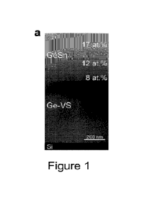
Figures 1(a-e). (a) Cross-sectional TEM image along the [110] zone axis of the
GeSn 17/12/8 at.%
(TL/ML/BL) multi-layer stacking grown on the Ge-VS/Si substrate. (b) XRD-RSM
around the
asymmetrical (224) reflection for the as-grown Geo 83Sno 17 sample. (c)
Schematics of the microdisk
fabrication process. (d) SEM image of the Geo 83Sil0 17 micro-disks (37.5
tilting angle). (e) Raman spectra
for Geo 83Sno 17 acquired on the as-grown (blue curve) and on the central
portion of the microdisk (red curve).
Figure 2. Schematic depicting the GeSn under-etch-induced relaxation and flake
transfer onto semi-
insulating substrate.
Figures 3(ac). Optical images of as-grown GcSn heterostructurc (a), as-
transferred GcSn membrane (b). (c)
and (d) show the corresponding Raman maps recorded using Ge-Ge mode; (e)
Individual Ge-Ge spectra
measured for as-grown heterostructure (black curve), partially detached
membrane (red curve), and fully
detached membrane (blue curve).
Figures 4. Optical image of as-transferred membrane along with Ge-Ge Raman
mode map, the strain
distribution and the calculated bandgap energy map.
Figure 5. Scanning electron microscopy image of as-transferred GeSn membranes
(top). Optical image of a
photodetector fabricated using transferred GeSn membrane (bottom). Inset: A
close-up image showing the
membrane underneath the contact fingers.
Figures 6(a-b). (a) IV curves for the total current and the photocurrent of
the photodetector. (b) The spectral
responsivity for the relaxed transferred PD compared to another PD made of as
grown GeSn.
Figure 7. Performance of a variety of GeSn short-wave infrared and mid-wave
infrared photodetectors
fabricated using layers at different Sn content and lattice strain.
CA 03177142 2022- 10- 27
WO 2021/217256
PCT/CA2021/050579
17
Figures 8(a-b). (a) PL spectra and absorption coefficient squared (A2) at 300
K for the as-grown Geo 83SnO 17
and (b) micro-disk samples. In the A2 curves, the intercept of the straight
dashed line extrapolates the energy
of the optical transition(s).
Figures 9(a-d). (a-b) SEM images the Geo 83Sno 17 micro-disk arrays (37.5
tilting angle) showing few micro-
disks that are detached from the Ge-VS and redeposited in a different
location. (c) Raman maps indicating
the complete GeSn and Ge-VS removal in between the micro-disks and (d) the
peak position across the
individual micro-disks.
Figure 10. Schematics of the optical setup use for transmission measurements.
A supercontinuum laser has
been used as a white light source with emission up to 4.1 JAM or has been
replaced by the internal glow bar
of the FTIR system for measurements further in the infrared. The emission of
the source was then coupled
through the interferometer and focused onto the sample which was placed at the
entrance of a gold-coated
integrating sphere. The light was collected from the integrating sphere
through a baffled port and focused
onto an HgCdTe-detector. Background measurements have been performed directly
before each
transmission measurement and the total transmission was determined as Ttot =
IT
ems, - background-
Figures 11(a-b). Schematics of all reflections taken into account for the
dctcrmination of thc total
transmission Ttot. Where in (a) only the reflections at the outside of the
samples are taken into account (see
equation S4) and in (b) the additional reflection on the germanium-silicon
interface (see equation S5). In
this figure tx is a transmission through a respective medium, Rx is a
reflection between two media and R.;
and T; are the effective reflection and transmission through a layer taking
into account multiple reflections.
Figures 12(a-b). (a) Relation between the measured transmission Tt0t and the
transmission due to non-
absorbed light ttot and the relation between Ttot and (b) the absorbance
(equation S3) of the measured GcSn
samples. In these graphs no reflections at interfaces are taken into account
(black line), only reflections at
the air-sample interfaces are taken into account (solid blue line, equation
S4) and air-sample interfaces and
the Ge-Si interface inside the sample are taken into account (orange dashed
line and see equation S5). All
graphs are calculated using refractive indices of n3=3 .4 and nGe=4.2.
Figures 13(a-c). (a) The transmittance and absorbance of the as-grown Geo
83Snoi7 sample, measured using
a supercontinuum source. (b) The transmittance and absorbance of the Geo
83Sil0.17 micro-disks, measured
using a glow bar. (c) The transmittance and absorbance of the as-grown
Ge0863Sno137 sample, measured
using a supercontinuum source. The A2 curve is a derived function from
transmission data according to the
procedure described in the supporting information.
CA 03177142 2022- 10- 27
WO 2021/217256
PCT/CA2021/050579
18
Figures 14(a-b). Extrapolated 8-band kp band gap value at 300 K based on the
temperature dependence of
the PL emission (shown in Figures 4 and 5) for strained and relaxed (a) Geo
83Sno 17 and (b) Geo 88SnO 12.
Figures 15(a-c). (a) PL spectra acquired using excitation power densities from
6.9 W/cm2 to 5.4 kW/cm2.
Plot of the (b) integrated PL intensity and (c) emission energy as a function
of the excitation power density.
Figure 16. Mass spectrum extracted from the APT measurements of Gen 83SI10 17.
Figure 17. Micrograph of a light-emitting diode.
Figure 18. Signal intensity compared for EL and PL from a fabricated LED
device and PL from an as-grown
sample.
Figure 19. Micrograph of a GeSn PIN photodetector.
Figure 20(a-c). (a) Spectral responsivity for GeSn PIN device at RT and 78 K
along with RT PL for the as-
grown sample; (b) detectivity comparison of the Ex-InGaAs at RT with GeSn
device at RT and 78 K; and
(c) IV for dark current for various devices diameters at 78 K compared to Ex-
InGaAs at RT.
DETAILED DESCRIPTION
In the following description, similar features in the drawings have been given
similar reference numerals.
In order to not unduly encumber the figures, some elements may not be
indicated on some figures if they
were already mentioned in preceding figures. It should also be understood
herein that the elements of the
drawings are not necessarily drawn to scale and that the emphasis is instead
being placed upon clearly
illustrating the elements and structures of the present embodiments.
The terms -an" and -one" are defined herein to mean -at least one",
that is, these terms do not exclude
a plural number of items, unless stated otherwise.
Terms such as "substantially", "generally" and "about", that modify a value,
condition or characteristic of
a feature of an exemplary embodiment, should be understood to mean that the
value, condition or
characteristic is defined within tolerances that are acceptable for the proper
operation of this exemplary
embodiment for its intended application.
Unless stated otherwise, the terms "connected- and "coupled", and derivatives
and variants thereof, refer
herein to any structural or functional connection or coupling, either direct
or indirect, between two or more
elements. For example, the connection or coupling between the elements may be
acoustical, mechanical,
optical, electrical, logical, or any combination thereof
CA 03177142 2022- 10- 27
WO 2021/217256
PCT/CA2021/050579
19
In the present description, the terms "light" and "optical", and variants and
derivatives thereof, are used to
refer to radiation in any appropriate region of the electromagnetic spectrum.
The terms "light" and "optical"
are therefore not limited to visible light, but can also include, without
being limited to, the infrared region
of the electromagnetic spectrum. For example, in some implementations, the
present techniques can be used
with electromagnetic signals having wavelengths ranging from about 700 nm to
about 30 nm (referred to as
the "infrared portion of the electromagnetic spectrum"), and more particularly
from about 1 nm to
about 8 nm (referred to as the "short-wave infrared and mid-wave infrared
portion of the electromagnetic
spectrum"). However, this range is provided for illustrative purposes only and
some implementations of the
present techniques may operate outside this range. Also, the skilled person
will appreciate that the definition
of the ultraviolet, visible and infrared ranges in terms of spectral ranges,
as well as the dividing lines between
them, may vary depending on the technical field or the definitions under
consideration, and are not meant
to limit the scope of applications of the present techniques.
The expression "heterostructure" will be used throughout the description and
refers to a structure including
at layers with different composition, lattice strain and/or electronic
properties. In some implementations,
the heterostructure may include at least two group W alloy-based lavers.
The expression "device" refers to a component or an assembly associated with a
functionality. For example,
an -optoelectronic device" is a device that can accomplish a specific
functionality involving the use or
manipulation of both charge carriers and photons (e.g., lasers, light emitting
diodes, photodetectors, solar
cells, sensors and imagers, and others). Many other types of devices exist,
such as, and without being
limitative ultrafast transistors, quantum information devices, spintronics
devices, energy conversion
devices, sensors and imagers, and hybrid photonics-electronics devices.
The expression "strained lattice" will be used when the lattice parameter in
at least one crystallographic
direction is different than the value at equilibrium. In this context, the
lattice is said to be "stretched" when
the lattice parameter is larger than the value at equilibrium, and the lattice
is said to be "compressed" when
the lattice parameter is smaller than the value at equilibrium. As such, the
expression "strain- will be used
to reflect a relative change in lattice parameter with respect to its
equilibrium value. It is to be noted that the
expressions "lattice constant" and "lattice parameter", which will be used
interchangeably, refer to the
equilibrium interatomic distance along a specific crystallographic direction
in a crystalline material. A layer
or a heterostnicture is said to be relaxed when its lattice parameters undergo
a transition from strained state
to reach values close or equal to those at the equilibrium. This transition
may occur during growth or by
post-growth release.
The group IV elements are the elements of column IV of the periodic table,
e.g., C, Si, Ge, Sn and Pb and
their stable isotopes.
CA 03177142 2022- 10- 27
WO 2021/217256
PCT/CA2021/050579
The term "alloy" refers to a material or a composition including at least two
different elements. For example,
and without being limitative, an alloy could include two, three or four
different elements. In some
implementations, the alloys may include at least two group IV elements.
The term "p-type doping" refers to the incorporation of an impurity in the
growing layer to create an excess
of positive charges known as holes. The term "n-type doping" refers to the
incorporation of an impurity in
the growing layer to create an excess of negative charges known as electrons.
The term -intrinsic doping
(i)- refers to the case where a semiconductor layer has no excess negative or
positive charges.
The terms "p-n junction" or "n-p junction" refer to two successive layers,
wherein one layer is p-type doped
and the other one is n-type doped. The terms "p-i-n junction" or
junction" refer to three successive
layers, wherein one layer is p-type doped, one is intrinsic, and one is n-type
doped.
Theoretical context
Free-space optical communications, infrared harvesting, biological and
chemical sensing, and imaging
technologies would strongly benefit from the availability of scalable, cost-
effective, and silicon- (Si-)
compatible short-wave infrared and mid-wave infrared optoelectronic devices.
With this perspective, Sn-
containing group IV semiconductors, such as, for example GeSn grown on Si
wafers have recently been the
subject of extensive investigations, as exemplified in references 1 to 5. At
the core of these expended efforts
is the ability to harness the relatively efficient direct band gap emission
from these emerging
semiconductors, which can be achieved at a Sn content around 10 at.% in fully
relaxed layers. It is, however,
noteworthy that this critical content is significantly above the about 1 at.%
equilibrium solubility of Sn in
Ge, which calls for a precise control of the growth kinetics to prevent phase
separation and avoid Sn
segregation and material degradation. Moreover, the epitaxial growth of GeSn
is typically achieved on Si
wafers using a Ge interlayer - commonly known as a "Ge virtual substrate-
(which will be referred to as
"Ge-VS" or "virtual substrate" in the present description), resulting in
inherently compressively strained
GeSn layer(s) [see references 6 and 71, thus increasing the Sn content
threshold for the indirect-to-direct
band gap crossover, and, as a result, the associated optical emission is
shifted to higher energies [see
references 8 to 101. In some cases, this behavior is also associated with a
broadening of the emission peak
and a decrease in its intensity as a result of the degradation in the material
quality at high Sn contents.
Moreover, the strain in the GeSn epitaxial layers was found to affect the
incorporation of Sn throughout the
growth, which can lead to graded composition as the layers grow thicker [see
references 6,71.
Among the strategies to circumvent the GeSn growth hurdles, lattice parameter
engineering using multi-
layer and step-graded growth has been shown to be effective in controlling the
Sn content and its uniformity.
This process was exploited in recent studies demonstrating room-temperature
optical emission and detection
CA 03177142 2022- 10- 27
WO 2021/217256
PCT/CA2021/050579
21
down to 0.36 eV (approximately 3.4 gm wavelength), see for example reference
4, as well as optically-
pumped lasing operating between about 3.1 gm to about 3.4 gm at temperatures
in the range of about 180
K to about 270 K (see for example references 11 to 13). In addition to lattice
parameter engineering during
the growth, post-growth control and manipulation of strain has also been
utilized to extend the emission
range as longer wavelengths can be achieved through relaxation and tensile
strain engineering.
Notwithstanding the contributions from these recent studies, the current GcSn-
based photodetector
technology is still limited to a range below 4 gm and with a very limited
performance at room temperature.
The technology and its advantages will become more apparent from the detailed
description and examples
that follow, which describe the various embodiments of the technology.
Short-wave infrared and mid-wave infrared optoelectronic device and related
methods
In accordance with one aspect, there is provided an optoelectronic device
having an operation range reaching
and exceeding 4 gm and operable at room temperature or at a cryogenic
temperature. Optoelectronic devices
such as described herein may include a silicon-based substrate and a
heterostructure extending over at least
a portion of the silicon-based substrate. The heterostructure may include a
stack of coextending photoactive
layers and each photoactive layer may include one or two group IV elements. In
some implementations, the
photoactive layers are configured for absorbing and/or emitting short-wave
infrared and mid-wave infrared
radiation. In some implementations, the short-wave infrared and mid-wave
infrared radiation is in a
wavelength range extending from 1 gm to-8 gm. In some embodiments, the group
IV elements are selected
from the group consisting of: Si, Ge and Sn. In some embodiments, the
wavelength range extends from
about 2 gm to about 8 gm. In some embodiments, the wavelength range extends
from about 1 gm to about
1.7 vim. In some embodiments, the wavelength range extends from about 1 vim to
about 2.7 gm. In some
embodiments, the wavelength range extends from about 1 gm to about 3.3 gm. In
some embodiments, the
wavelength range extends from about 1 gm to about 3.5 gm. In some embodiments,
the wavelength range
extends from about 1 vim to about 4.7 vim.
In accordance with another aspect, there is provided a method for
manufacturing an optoelectronic device.
The method includes conditioning a reactor chamber to reach initial growth
conditions. The method includes
forming a heterostructure on a substrate provided inside the reactor chamber,
which may include forming a
first GeSn layer by exposing the substrate to the initial growth conditions,
conditioning the reactor chamber
to reach subsequent growth conditions and forming at least one subsequent GeSn
layer on the GeSn layer
by exposing the first GeSn layer to the subsequent growth conditions, each
GeSn layer in the heterostructure
having a different Sn content one from another. The method includes releasing
the heterostructure from the
substrate to form a relaxed membrane and transferring the relaxed membrane on
a host substrate. In some
embodiments, the method includes patterning the heterostructure to obtain an
array of structures. In one
CA 03177142 2022- 10- 27
WO 2021/217256
PCT/CA2021/050579
22
nonlimitative example, the array of structures is an array of micro-disks. In
some embodiments, the substrate
includes a virtual substrate layer extending over an original substrate layer
and the step of releasing the
heterostructure from the substrate includes etching portions of the
heterostructure and the virtual substrate
until the heterostructure collapses on the original substrate. In some
embodiments, the step of etching the
portions of the heterostructure and the virtual substrate includes
anisotropically etching the portions of the
heterostructure and portions of the virtual substrate with C12, and
anisotropically etching remaining portions
of the virtual substrate with CF4. In some embodiments, the method includes
forming a metallic contact
operatively connecting the heterostructure with the substrate.
In some implementations, the optoelectronic device is a GeSn-based
photodetector on a Si substrate. For
example, the photodetector may include (Si)GeSn-based heterostructure(s),
which may either be undoped
or doped, and forming p-i-n junctions.
In some implementations, the optoelectronic device is a Ge Sn-based light-
emitting diode on a Si substrate.
Optoelectronic devices as described herein are examples of group IV integrated
optoelectronic or photonic
devices operating in the short-wave infrared and mid-wave infrared range that
may serve as platforms for
scalable, compact, and silicon-compatible technologies. In some
implementations, the photodetectors may
be incorporated in sensors and imaging devices.
In accordance with another aspect, there is also provided a method for
manufacturing such optoelectronic
devices and photodetectors. The method may include strain-engineering the
heterostructure, either during
the epitaxial growth or after the epitaxial growth, i.e., during the
processing of the optoelectronic device or
photodetector. In some implementations, the method may include releasing the
heterostructure from the
substrate to form membrane photodetectors. In some implementations, the method
may include transferring
the membrane photodetectors on a host substrate, i.e., a substrate different
than the substrate on which the
heterostructure has been grown onto. Examples of host substrates include, but
are not limited to oxidized
surfaces, transparent substrates, biological surfaces, and/or flexible
substrates. In some implementations,
the method may include independently engineering the strain and the
composition of the heterostructure. In
some implementations, the method may be used for manufacturing photodetectors
on silicon, the
photodetectors having a wavelength cut-off exceeding 4 um at room temperature.
The method as described
herein is a silicon-compatible technology and may be associated with a wealth
of opportunities for relatively
low-cost and relatively high-performance short-wave infrared and mid-wave
infrared sensing and imaging
applications.
In accordance with another aspect, there is provided an optoelectronic device
including a silicon-based
substrate, a heterostructure at least partially extending over the silicon-
based substrate and electrodes
CA 03177142 2022- 10- 27
WO 2021/217256
PCT/CA2021/050579
23
operatively connected to the heterostructure. The heterostructure includes a
stack of coextending
photoactive layers, each photoactive layer including at least two group IV
elements and being configured
for absorbing short-wave infrared and mid-wave infrared radiation, the short-
wave infrared and mid-wave
infrared radiation being in a wavelength range extending from about 1 um to
about 8 um.
In some embodiments, said at least two group IV elements are selected from the
group consisting of: Si, Ge
and Sn. In some embodiments, the wavelength range extends from about 2 um to
about 8 um. In some
embodiments, the wavelength range extends from about 1 um to about 1.7 um. In
some embodiments, the
wavelength range extends from about 1 um to about 2.7 um. In some embodiments,
the wavelength range
extends from about 1 um to about 3.3 um. In some embodiments, the wavelength
range extends from about
1 um to about 3.5 11M. In some embodiments, the stack of coextending
photoactive layers includes at least
one GeSn-based layer. In some embodiments, the stack of coextending
photoactive layers includes at least
two GeSn-based layers, each of said at least two GeSn-based layers having a
different chemical composition
one from another. In some embodiments, the different chemical composition
includes an Sn content. In
some embodiments, the Sn content of said at least two Ge Sn-based layers is
included in a range extending
between 1 at% and 25 at%. In some embodiments, each of said at least two GeSn-
based layers has a different
lattice strain one from another. In some embodiments, the optoelectronic
device, further includes a Ge
virtual substrate extending over the silicon-based substrate. In some
embodiments, the optoelectronic device
is operable at room temperature. In some embodiments, the optoelectronic
device is operable at a cryogenic
temperature. In some embodiments, the cryogenic temperature is equal or
greater than about 77 K. In some
embodiments, each photoactive layer has a strain included in a range extending
between about -2 %to about
+2%.
In accordance with another aspect, there is provided a photodetector including
a silicon-based substrate, a
heterostructure at least partially extending over the silicon-based substrate
and electrodes operatively
connected to the heterostructure. The heterostructure includes a stack of
coextending photoactive layers,
each photoactive layer including at least two group IV elements and being
configured for detecting short-
wave infrared and mid-wave infrared radiation, the short-wave infrared and mid-
wave infrared radiation
being in a wavelength range extending from about to about 8 um.
In some embodiments, said at least two group IV elements are selected from the
group consisting of: Si, Ge
and Sn. In some embodiments, the wavelength range extends from about 2 um to
about 8 [an. In some
embodiments, the wavelength range extends from about 1 I1M to about 1.7 11M.
In some embodiments, the
wavelength range extends from about 1 ilM to about 2.7 11M. In some
embodiments, the wavelength range
extends from about 1 I1M to about 3.3 JAM. In some embodiments, the wavelength
range extends from about
1 um to about 3.5 um. In some embodiments, the stack of coextending
photoactive layers includes at least
one GeSn-based layer. In some embodiments, the stack of coextending
photoactive layers includes at least
CA 03177142 2022- 10- 27
WO 2021/217256
PCT/CA2021/050579
24
two Ge Sn-based layers, each of said at least two GeSn-based layers having a
different chemical composition
one from another. In some embodiments, the different chemical composition
includes an Sn content. In
some embodiments, the Sn content of said at least two Ge Sn-based layers is
included in a range extending
between 1 at% and 25 at%. In some embodiments, each of said at least two GeSn-
based layers has a different
lattice strain one from another. In some embodiments, the photodetector,
further includes a Ge virtual
substrate extending over the silicon-based substrate. In some embodiments, the
photodetector is operable at
room temperature. In some embodiments, the optoelectronic device is operable
at a cryogenic temperature.
In some embodiments, the cryogenic temperature is equal or greater than about
77 K. In some embodiments,
each photoactive layer has a strain included in a range extending between
about -2 % to about +2%.
In accordance with another aspect, there is provided a light-emitting diode,
including a silicon-based
substrate, a heterostructure at least partially extending over the silicon-
based substrate and electrodes
operatively connected to the heterostructure. The heterostructure includes a
stack of coextending
photoactive layers, each photoactive layer including at least two group IV
elements and being configured
for emitting short-wave infrared and mid-wave infrared radiation, the short-
wave infrared and mid-wave
infrared radiation being in a wavelength range extending from about 1 uni to
about g um.
In some embodiments, said at least two group IV elements are selected from the
group consisting of: Si, Ge
and Sn. In some embodiments, wavelength range extends from about 2 um to about
8 um. In some
embodiments, the wavelength range extends from about 1 um to about 1.7 um. In
some embodiments, the
wavelength range extends from about 1 um to about 2.7 um. In some embodiments,
the wavelength range
extends from about 1 tun to about 3.3 tun. In some embodiments, the wavelength
range extends from about
1 um to about 3.5 I1M . In some embodiments, the stack of coextending
photoactive layers includes at least
one GeSn-based layer. In some embodiments, the stack of coextending
photoactive layers includes at least
two Ge Sn-based layers, each of said at least two GeSn-based layers having a
different chemical composition
one from another. In some embodiments, the different chemical composition
includes an Sn content. In
some embodiments, the Sn content of said at least two GeSn-based layers is
included in a range extending
between 1 at% and 25 at%. In some embodiments, each of said at least two GeSn-
based layers has a different
lattice strain one from another. In some embodiments, the light-emitting diode
further includes a Ge virtual
substrate extending over the silicon-based substrate. In some embodiments, the
light-emitting diode is
operable at room temperature. In some embodiments, the optoelectronic device
is operable at a cryogenic
temperature. In some embodiments, the cryogenic temperature is equal or
greater than about 77 K. In some
embodiments, each photoactive layer has a strain included in a range extending
between about -2 %to about
+2%.
In accordance with another aspect, there is provided an optoelectronic
platform, including a silicon-based
substrate, a heterostructure at least partially extending over the silicon-
based substrate and electrodes
CA 03177142 2022- 10- 27
WO 2021/217256
PCT/CA2021/050579
operatively connected to the heterostructure. The heterostructure includes a
stack of coextending
photoactive layers, each photoactive layer including at least two group IV
elements and being configured to
perform at least one of emitting short-wave infrared and mid-wave infrared
radiation and detecting the short-
wave infrared and mid-wave infrared radiation. The short-wave infrared and mid-
wave infrared radiation is
in a wavelength range extending from about 1 p.m to about 8 p.m.
In some embodiments, said at least two group IV elements are selected from the
group consisting of: Si, Ge
and Sn. In some embodiments, the wavelength range extends from about 2 pm to
about 8 pm. In some
embodiments, the wavelength range extends from about 2 p.m to about 2.8 p.m.
In some embodiments, the
wavelength range extends from about 1 p.m to about 1.7 p.m. In some
embodiments, the wavelength range
extends from about 1 pm to about 2.7 p.m. In some embodiments, the wavelength
range extends from about
1 jam to about 3.3 p.m. In some embodiments, the wavelength range extends from
about 1 jam to about
3.5 nm. In some embodiments, the stack of coextending photoactive layers
includes at least one GeSn-based
layer. In some embodiments, the stack of coextending photoactive layers
includes at least two Ge Sn-based
layers, each of said at least two GeSn-based layers having a different
chemical composition one from
another. In some embodiments, the different chemical composition includes an
Sn content. In some
embodiments, the Sn content of said at least two GeSn-based layers is included
in a range extending between
1 at% and 25 at%. In some embodiments, each of said at least two GeSn-based
layers has a different lattice
strain one from another. In some embodiments, the optoelectronic platform
further includes a Ge virtual
substrate extending over the silicon-based substrate. In some embodiments, the
optoelectronic platform is
operable at room temperature. In some embodiments, the optoelectronic device
is operable at a cryogenic
temperature. In some embodiments, the cryogenic temperature is equal or
greater than about 77 K. In some
embodiments, each photoactive layer has a strain included in a range extending
between about -2 %to about
+2%.
In accordance with another aspect, there is provided a method for
manufacturing an optoelectronic device.
The method includes conditioning a reactor chamber to reach initial growth
conditions and forming a
heterostructure on a substrate provided inside the reactor chamber. The step
of forming the heterostructure
includes forming a first group IV alloy layer by exposing the substrate to the
initial growth conditions;
conditioning the reactor chamber to reach subsequent growth conditions; and
forming at least one
subsequent group IV alloy layer on the group IV alloy layer by exposing the
first group IV alloy layer to
the subsequent growth conditions, each group IV alloy layer in the
heterostructure having a different or
relatively similar Sn content one from another. The method further includes
releasing thc heterostructure
from the substrate to form a relaxed membrane and transferring the relaxed
membrane on a host substrate.
In some embodiments, the group IV alloy layers includes at least two group IV
elements selected from the
group consisting of Si, Ge and Sn. In some embodiments, the method further
includes n-doping at least one
CA 03177142 2022- 10- 27
WO 2021/217256
PCT/CA2021/050579
26
of the group IV alloy layers. In some embodiments, the method further includes
p-doping at least one of the
group IV alloy layers. In some embodiments, the method further includes
forming group IV alloy multi-
quantum wells. In some embodiments, the method further includes patterning the
heterostructure to obtain
an array of structures. In some embodiments, the substrate includes a virtual
substrate layer extending over
an original substrate layer and wherein said releasing the heterostructure
from the substrate includes etching
portions of the heterostructure and the virtual substrate until the
heterostructure collapses on the original
substrate. In some embodiments, said etching the portions of the
heterostructure and the virtual substrate
includes: anisotropically etching the portions of the heterostructure and
portions of the virtual substrate with
C12; and isotropically etching remaining portions of the virtual substrate
with CF4. In some embodiments,
the method further includes forming a metallic contact operatively connecting
the heterostructure with the
substrate. In some embodiments, said forming the heterostructure includes
forming at least one GeSn-based
layers. In some embodiments, said forming the heterostructure includes forming
at least two GeSn-based
layers, each of said at least two GeSn-based layers having a different
chemical composition one from
another. In some embodiments, the different chemical composition includes an
Sn content. In some
embodiments, the Sn content of said at least two GeSn-based layers is included
in a range extending between
1 at% and 25 at%. In some embodiments, each of said at least two GeSn-based
layers has a different lattice
strain one from another. In some embodiments, there is provided an
optoelectronic device manufactured
according to the method herein described.
In accordance with another aspect, there is provided a method for
manufacturing an optoelectronic device.
The method includes forming a heterostructure on a substrate provided inside a
reactor chamber. The step
of forming the heterostructure includes forming a first group IV alloy layer
by exposing the substrate to
initial growth conditions; and forming at least one subsequent group IV alloy
layer on the group IV alloy
layer. The method further includes varying a precursor concentration inside
the reactor chamber while
forming the heterostructure to obtain subsequent growth conditions, such that
each group IV alloy layer in
the heterostructure has a different Sn content one from another upon exposure
to the subsequent growth
conditions.
In some embodiments, the group IV alloy layers includes at least two group IV
elements selected from the
group consisting of Si, Ge and Sn. In some embodiments, the method further
includes n-doping at least one
of the group IV alloy layers. In some embodiments, the method further includes
p-doping at least one of the
group IV alloy layers. In some embodiments, the method further includes
forming group IV alloy multi-
quantum wells. In some embodiments, the method further includes patterning the
heterostructure to obtain
an array of structures. In some embodiments, the method further includes
forming a metallic contact
operatively connecting the heterostructure with the substrate. In some
embodiments, said forming the
heterostructure includes forming at least one GeSn-based layers. In some
embodiments, said forming the
heterostructure includes forming at least two Ge Sn-based layers, each of said
at least two GeSn-based layers
CA 03177142 2022- 10- 27
WO 2021/217256
PCT/CA2021/050579
27
having a different chemical composition one from another. In some embodiments,
the different chemical
composition includes an Sn content. In some embodiments, the Sn content of
said at least two GeSn-based
layers is included in a range extending between I at% and 25 at%. In some
embodiments, each of said at
least two GeSn-based layers has a different lattice strain one from another.
In some embodiments, there is
provided an optoelectronic device manufactured according to the method herein
described.
In accordance with another aspect, there is provided alight-emitting diode.
The light-emitting diode includes
a silicon-based substrate, a heterostructure at least partially extending over
the silicon-based substrate and
electrodes operatively connected to the heterostructure. The heterostructure
includes a stack of coextending
photoactive layers, each photoactive layer including at least two group IV
elements and being configured
for emitting short-wave infrared and mid-wave infrared radiation, the short-
wave infrared and mid-wave
infrared radiation being in a wavelength range extending from about 2 ttm to
about 2.8 ttm.
In some embodiments, the light-emitting diode has a diameter of about 40 ttm.
In some embodiments, the
stack of coextending photoactive layers includes at least one GeSn-based
layer. In some embodiments, the
stack of coextending photoactive layers includes at least two GeSn-based
layers, each of said at least two
GeSn-based layers having a different chemical composition one from another. In
some embodiments, the
different chemical composition includes an Sn content. In some embodiments,
the Sn content of said at least
two GeSn-based layers is included in a range extending between 1 at% and 25
at%. In some embodiments,
each of said at least two GeSn-based layers has a different lattice strain one
from another. In some
embodiments, each of said at least two GeSn-based layers has a different
thickness one from another. In
some embodiments, the light-emitting diode further includes a Ge virtual
substrate extending over the
silicon-based substrate. In some embodiments, the light-emitting diode is
operable at room temperature. In
some embodiments, the optoelectronic device is operable at a cryogenic
temperature. In some embodiments,
the cryogenic temperature is equal or greater than about 77 K. In some
embodiments, each photoactive
layer has a strain included in a range extending between about -2 % to about
+2%.
In accordance with another aspect, there is provided a photodetector. The
photodetector includes a silicon-
based substrate, a heterostructure at least partially extending over the
silicon-based substrate and electrodes
operatively connected to the heterostructure. The heterostructure includes a
stack of coextending
photoactive layers, each photoactive layer including at least two group IV
elements and being configured
for detecting short-wave infrared and mid- wave infrared radiation, the short-
wave infrared and mid- wave
infrared radiation being in a wavelength range extending from about 1 ttm to
about 2.6 ttm.
In some embodiments, the photodetector has a diameter included in a range
extending from about 20 tim to
about 160 tun. In some embodiments, the stack of coextending photoactive
layers includes at least one
GeSn-based layer. In some embodiments, the stack of coextending photoactive
layers includes at least two
GeSn-based layers, each of said at least two GeSn-based layers having a
different chemical composition
CA 03177142 2022- 10- 27
WO 2021/217256
PCT/CA2021/050579
28
one from another. In some embodiments, the different chemical composition
includes an Sn content. In
some embodiments, the Sn content of said at least two Ge Sn-based layers is
included in a range extending
between 1 at% and 25 at%. In some embodiments, each of said at least two GeSn-
based layers has a different
lattice strain one from another. In some embodiments, the photodetector
further includes a Ge virtual
substrate extending over the silicon-based substrate. In some embodiments, the
photodetector is operable at
room temperature. In some embodiments, the optoelectronic device is operable
at a cryogenic temperature.
In some embodiments, the cryogenic temperature is equal or greater than about
77 K. In some embodiments,
each photoactive layer has a strain included in a range extending between
about -2 % to about +2%.
In accordance with another aspect, there is provided a method for
manufacturing an optoelectronic device.
The method includes conditioning a reactor chamber to rcach initial growth
conditions and forming a
heterostructure on a substrate provided inside the reactor chamber. The step
of forming the heterostructure
includes forming a first group IV alloy layer by exposing the substrate to the
initial growth conditions;
conditioning the reactor chamber to reach subsequent growth conditions; and
forming at least one
subsequent group IV alloy layer on the group IV alloy layer by exposing the
first group IV alloy layer to
the subsequent growth conditions, each group IV alloy layer in the
heterostructure having a different or
relatively similar Sn content one from another. The method further includes
patterning the heterostructure
and etching the heterostructure to expose a portion of the substrate,
patterning the heterostructure and
etching the heterostructure to expose a portion of one of the first group IV
alloy layer and said at least one
subsequent group IV alloy layer, passivating the heterostructure, etching
contacts holes on the substrate
through the heterostructure and depositing metal in the contact holes to form
electrical contacts of the
optoelectronic device.
In some embodiments, the group IV alloy layers includes at least two group IV
elements selected from the
group consisting of Si, Ge and Sn. In some embodiments, the method further
includes n-doping at least one
of the group IV alloy layers with a group V element. In some embodiments, the
method further includes p-
doping at least one of the group IV alloy layers with a group III element. In
some embodiments, the method
further includes forming group IV alloy multi-quantum wells. In some
embodiments, the method further
includes patterning the heterostructure to obtain an array of structures. In
some embodiments, the method
further includes forming a metallic contact operatively connecting the
heterostructure with the substrate. In
some embodiments, said forming the heterostructure includes forming at least
one GeSn-based layer. In
some embodiments, said forming the heterostructure includes forming at least
two Ge Sn-based layers, each
of said at least two GeSn-based layers having a different chemical composition
one from anothcr. In some
embodiments, the different chemical composition includes an Sn content. In
some embodiments, the Sn
content of said at least two Ge Sn-based layers is included in a range
extending between I at% and 25 at%.
In some embodiments, each of said at least two GeSn-based layers has a
different thickness and lattice strain
CA 03177142 2022- 10- 27
WO 2021/217256
PCT/CA2021/050579
29
one from another. In some embodiments, there is provided an optoelectronic
device manufactured according
to the method herein described.
In accordance with another aspect, there is provided a method for
manufacturing a waveguide. The method
includes conditioning a reactor chamber to reach initial growth conditions and
forming a heterostructure on
a substrate provided inside the reactor chamber. The step of forming the
heterostructure includes forming
a first group IV alloy layer by exposing the substrate to the initial growth
conditions; conditioning the reactor
chamber to reach subsequent growth conditions; and forming at least one
subsequent group IV alloy layer
on the group IV alloy layer by exposing the first group IV alloy layer to the
subsequent growth conditions,
each group IV alloy layer in the heterostructure having a different or
relatively similar Sn content one from
anothcr. The method further includes patterning the heterostructure and
etching the hcterostructurc to expose
a portion of the substrate and patterning the heterostructure and etching the
heterostructure to expose a
portion of one of the first group IV alloy layer and said at least one
subsequent group IV alloy layer.
In some embodiments, the group IV alloy layers includes at least one group IV
element selected from the
group consisting of Si, Ge and Sn. In some embodiments, the method further
includes n-doping at least one
of the group IV alloy layers with a group V element. In some embodiments, the
method further includes p-
doping at least one of the group IV alloy layers with a group III element. In
some embodiments, the method
further includes forming group IV alloy heterostructures. In some embodiments,
the method further includes
forming group IV alloy multi-quantum wells. In some embodiments, the substrate
includes a virtual
substrate layer extending over an original substrate layer, the method further
including forming a waveguide
by etching portions of the heterostructure and the virtual substrate. In some
embodiments, said etching the
portions of the heterostructure and the virtual substrate includes
isotropically etching the portions of the
heterostructure and portions of the virtual substrate with C12. In some
embodiments, said etching the portions
of the heterostructure and the virtual substrate includes isotropically
etching portions of the heterostructure
and portions of the virtual substrate with CF4.
In accordance with another aspect, there is provided a monolithic platform for
on-chip emission and
detection of infrared light. The monolithic platform includes a silicon-based
substrate, a light-emitting diode
as herein described, a photodetector as herein described and a waveguide
connecting the light-emitting diode
and the photodetector.
In some embodiments, the wavelength range extends from about 1 p.m to about 8
p.m. In some embodiments,
the monolithic platform is operable at room temperature. In some embodiments,
the optoelectronic device
is operable at a cryogenic temperature. In some embodiments, the cryogenic
temperature is equal or greater
than about 77 K.
In accordance with another aspect, there is provided a method for
manufacturing a light-emitting diode. The
method includes conditioning a reactor chamber to reach initial growth
conditions and forming a
CA 03177142 2022- 10- 27
WO 2021/217256
PCT/CA2021/050579
heterostructure on a substrate provided inside the reactor chamber. The step
of forming the heterostructure
includes forming a first group IV alloy layer by exposing the substrate to the
initial growth conditions;
conditioning the reactor chamber to reach subsequent growth conditions; and
forming at least one
subsequent group IV alloy layer on the group IV alloy layer by exposing the
first group IV alloy layer to
the subsequent growth conditions, each group IV alloy layer in the
heterostructure having a different or
relatively similar Sn content one from another. The method further includes
releasing the heterostructure
from the substrate to form a relaxed membrane and transferring the relaxed
membrane on a host substrate.
In some embodiments, the group IV alloy layers includes at least two group IV
elements selected from the
group consisting of Si, Gc and Sn. In some embodiments, the method further
includes n-doping at least onc
of the group IV alloy layers. in some embodiments, the method further includes
p-doping at least onc of the
group IV alloy layers. In some embodiments, the method further includes
forming group IV alloy multi-
quantum wells. In some embodiments, the method further includes patterning the
heterostructure to obtain
an array of structures. In some embodiments, the substrate includes a virtual
substrate layer extending over
an original substrate layer and wherein said releasing the heterostructure
from the substrate includes etching
portions of the heterostructure and the virtual substrate until the
heterostructure collapses on the original
substrate. In some embodiments, said etching the portions of the
heterostructure and the virtual substrate
includes anisotropically etching the portions of the heterostructure and
portions of the virtual substrate with
C12; and isotropically etching remaining portions of the virtual substrate
with CF4. In some embodiments,
the method further includes forming a metallic contact operatively connecting
the heterostructure with the
substrate. In some embodiments, said forming the heterostructure includes
forming at least one GeSn-based
layer. In some embodiments, said forming the heterostructure includes forming
at least two GeSn-based
layers, each of said at least two GeSn-based layers having a different
chemical composition one from
another. In some embodiments, the different chemical composition includes an
Sn content.
In some embodiments, the Sn content of said at least two GeSn-based layers is
included in a range extending
between 1 at% and 25 at%. In some embodiments, each of said at least two GeSn-
based layers has a different
lattice strain one from another. In some embodiments, there is provided a
light-emitting diode manufactured
according to the method herein described.
In accordance with another aspect, there is provided a method for
manufacturing a photodetector. The
method includes conditioning a reactor chamber to reach initial growth
conditions. The method also includes
forming a heterostructure on a substrate provided inside the reactor chamber.
The step of forming the
heterostructure includes forming a first group IV alloy layer by exposing the
substrate to the initial growth
conditions; conditioning the reactor chamber to reach subsequent growth
conditions; and forming at least
one subsequent group IV alloy layer on the group IV alloy layer by exposing
the first group IV alloy layer
to the subsequent growth conditions, each group IV alloy layer in the
heterostructure having a different or
CA 03177142 2022- 10- 27
WO 2021/217256
PCT/CA2021/050579
31
relatively similar Sn content one from another. The method further includes
releasing the heterostructure
from the substrate to form a relaxed membrane and transferring the relaxed
membrane on a host substrate.
In some embodiments, the group IV alloy layers includes at least two group IV
elements selected from the
group consisting of Si, Ge and Sn. In some embodiments, the method further
includes n-doping at least one
of the group IV alloy layers. In some embodiments, the method further includes
p-doping at least one of the
group IV alloy layers. In some embodiments, the method further includes
forming group IV alloy multi-
quantum wells. In some embodiments, the method further includes patterning the
heterostructure to obtain
an array of structures. In some embodiments, substrate includes a virtual
substrate layer extending over an
original substrate layer and wherein said releasing the heterostructure from
the substrate includes etching
portions of the hetcrostructure and the virtual substratc until the
heterostructure collapses on the original
substrate. In some embodiments, said etching the portions of the
heterostructure and the virtual substrate
includes: anisotropically etching the portions of the heterostructure and
portions of the virtual substrate with
Cl?; and isotropically etching remaining portions of the virtual substrate
with CF4.In some embodiments,
the method further includes forming a metallic contact operatively connecting
the heterostructure with the
substrate. In some embodiments, said forming the heterostructure includes
forming at least one GeSn-based
layer. In some embodiments, said forming the heterostructure includes forming
at least two GeSn-based
layers, each of said at least two GeSn-based layers having a different
chemical composition one from
another. In some embodiments, the different chemical composition includes an
Sn content. In some
embodiments, the Sn content of said at least two GeSn-based layers is included
in a range extending between
1 at% and 25 at%. In some embodiments, each of said at least two GeSn-based
layers has a different lattice
strain one from another. In some embodiments, there is provided a
photodetector manufactured according
to the method herein described.
In accordance with another aspect, there is provided an optoelectronic device,
including a silicon-based
substrate, a heterostructure and electrodes. The heterostructure at least
partially extends over the silicon-
based substrate, and includes one or more photoactive layers, each photoactive
layer including at least one
group IV element and being configured for absorbing short-wave infrared and
mid-wave infrared radiation,
the short-wave infrared and mid-wave infrared radiation being in a wavelength
range extending from about
1 um to about 8 um. The electrodes are operatively connected to the
heterostructure.
In some embodiments, said one or more photoactive layers includes a first
layer made of Ge and a second
layer made of Ge Sn, the second layer at least partially extending over the
first layer.
Examples and results
The section below provides examples of embodiments of a mid-wave infrared
optoelectronic device and
related methods, as well as examples of results related to embodiments of the
mid-wave infrared
CA 03177142 2022- 10- 27
WO 2021/217256
PCT/CA2021/050579
32
optoelectronic device and related methods. The following section should not be
interpreted as being
'imitative and serves an illustrative purpose only.
Besides the ability to engineer optoelectronic devices, the availability of
high quality GeSn layers also
provides a rich playground to tune the electronic and optical properties by
exploiting various physical
parameters. For instance, lattice strain and composition are always
interrelated in epitaxial GeSn layers and
play a key role in shaping the device performance. In some implementations,
there is provided a method to
tune these two parameters during growth or after growth. The epitaxial growth
is performed on silicon
wafers in a low-pressure chemical vapor deposition (CVD) reactor using ultra-
pure H.-, carrier gas, and 10%
monogenna.ne (Getti) and tin-tetrachloride (SnC14) precursors, similar to a
recently developed growth
protocol, which is described in the U.S. Provisional Patent Application No.:
62/856,500, the content of
which is incorporated by reference in its entirety. N-type and p-type doping
is achieved using As1-13 and
B2H6 precursors, respectively.
Optimization of GeSn material properties
The method for manufacturing the GeSn photodetectors allows independently
engineering the Sn content
and the lattice strain, which enables a relatively precise control of the
optoelectronic properties of the GeSn
device structures (i.e., the heterostructures). Figures 1(a-e) display an
example of as-grown GeSn layers
with a Sn content reaching 17%. In Figure 1(a), a cross-sectional TEM image
along the [110] zone axis of
the GeSn is shown. In this illustrated embodiment, the content of Sn in the
GeSn heterostructure is 17/12/8
at.%, for the top layer (TL), the middle layer (ML) and the bottom layer (BL),
respectively, and the GeSn
heterostructure is grown on s Ge-VS/Si substrate. The composition of each
layer is estimated from
Reciprocal Space Mapping (RSM) around the asymmetrical (224) X-ray diffraction
(XRD) peak, as
illustrated in Figure 1(b). The data indicate that the TL is under an in-plane
biaxial compressive strain cop-
1.3 %.
The method may include a step of etching the Ge-VS to significantly relax this
residual strain and releasing
the GeSn layers. In some implementations, the grown layers may be patterned
and etched to form 2.5 x2.5
mm2 arrays of GeSn micro-disks, as illustrated in Figure 1(c). In some
implementations, the anisotropic
reactive ion etching (RIE) of the sidewalls of the micro-disks was achieved
using C12, followed by selective
etching of the Ge-VS substrate using CFI in RIB.
The scanning electron microscope (SEM) image in Figure 1(d) exhibits atypical
array of micro-disks having
a diameter of about 7 larn and a pitch of about 10 gm. The apparent change in
the contrast of the outer rim
(about 1 lam in width) may be due to a partial over-etching of the 17 at.% TL
during the CF4 processing,
resulting from a non-uniform wetting of the negative resist. The CE4 etching
time is typically selected to
CA 03177142 2022- 10- 27
WO 2021/217256
PCT/CA2021/050579
33
completely release the GeSn micro-disks until they collapse on the Si wafer.
It is to be noted that a small
residual thickness of the Ge-VS layer may be visible on the Si substrate under
the micro-disk after the
fabrication process, see the Appendix A - Supporting Information. It is to be
noted that the presence of the
small residual thickness of the Ge-VS layer does not substantially affect the
strain in the GeSn micro-disks
because they are detached from the substrate. Raman measurements were
performed on the micro-disk
arrays to evaluate the residual strain in the GeSn TL. It is to be noted that
Raman spectra are recorded from
the TL without any contribution form the underlaying layers as the penetration
depth of the 633 nin
excitation laser (<30 nm) is significantly smaller than the TL thickness
(about 160 nm). Figure 1(e) displays
Raman spectra acquired at the center of a single GeSn micro-disk (red curve).
As a reference, the Raman
spectrum of the as-grown Geo 83Sno 17 layer is also shown (blue curve). The Ge-
Ge LO mode of the as-grown
layer is centered at about 292 cm-1, whereas the same mode shifts down to
about 287 cm-1 upon under-
etching. The observed about 5 cm-1 shift corresponds to a strain relaxation
from the as-grown value of about
-1.3 % down to about -0.2% in the GeSn micro-disks. It will be noted that the
Raman spectra associated
with the area between the GeSn micro-disks only show the Si-Si LO mode at
about 520 cm-1 from the
substrate (see the Appendix A - Supporting Information), indicating that the
Ge-VS was completely etched
leading to the observed strain relaxation. It will be noted that the measured
residual strain (-0.2%) in the TL
even after the complete release of the micro-disks is expected because the
GeSn stack includes, in the
illustrated embodiment, three layers with a variable composition. This post-
etching strain analysis is
consistent with our systematic studies decoupling Sn content and strain
effects on GeSn Raman vibrational
modes.
A relatively accurate theoretical framework to evaluate the band structure of
these multilayers is highly
coveted to elucidate or better understand the interplay between the
composition, strain, and structural
parameters for the investigated GeSn heterostructures. For instance, in order
to be able to quantitatively
interpret any spectroscopic related transitions, the band gaps in each layer
of the GeSn heterostructure (i.e.,
the TL, ML and BL) need to be estimated as a function of their respective
strain and Sn content. The 8-band
k-p model together with envelope function approximation (EFA) may be used to
that end (see reference 17)
The strain implementation is based on the Bir-Pikus formalism (see reference
18). Additionally, the model
solid theory was adopted to estimate the conduction and valence band offset
profiles of various high
symmetry bands (see references 19 and 20). It will be noted that the linear
interpolation formulae are
inaccurate to estimate the band gaps of binary compounds due to significant
bowing effects in the L and F
Brillouin zone directions. To circumvent this limitation, the bowing
parameters (at 0 K) hr = 1.94 and
= 1.23 were used. The obtained diagrams demonstrate that the electron and
holes diffuse into the
upmost 17 at.% layer, as a result of the band offset with the 12 at.% ML being
higher than 30 meV for both
electrons and heavy holes (HE). Besides, the TL layer strain relaxation (from
about -1.3% to about -0.2%)
induces an increase of 4-1' (= E:Lg ¨ ED by about 83 mcV, which may enhance
band to band
CA 03177142 2022- 10- 27
WO 2021/217256
PCT/CA2021/050579
34
recombination. Furthennore, the LH-1-1I-1 splitting is reduced by about 80 meV
in the TL layer. The valence
(conduction) band offset between the ML and TL are reduced (increased) by
about 14 meV (about 56 meV)
due to strain relaxation. For instance, Low et al. have shown using empirical
pscudopotential method that
the band gaps for the unstrained Ge083Sno17 at F and L brillouin directions
were equal to 0.42 eV and 0.45
eV which compares fairly well with the current k-p parametrization which gives
0.421 eV and 0.525 eV,
respectively (see reference 21). Additionally, based on Gupta's work (see
reference 8), the as-grown ML
layer (12% at. Sn, -0.54% compressive strain) is predicted to have a direct
band gap of 0.54 eV, which in
perfect agreement with our current kp model where the ML direct gap transition
is 0.574 eV. These
calculated results are used in design and implementation of devices discussed
below.
Photodetector device processing and optimization
As described below, the strain and composition of the GeSn heterostructures
may be independently
engineered, which may enable more flexibility to tune the optical properties
of GcSn. Photodetectors or
similar devices may be developed using this material system.
A variety of photodetectors using the as-grown GeSn heterostructures directly
on silicon substrates, as well
as released and transferred GeSn heterostructures have been produced. The
latter allows for an additional
strain relaxation.
Some aspects of the method for manufacturing a GeSn photodetector will now be
described.
In some implementations, the GeSn photodetector fabrication started by spin
coating a photoresist mask for
chlorine etch using ICP Oxford Instruments PlasmaLab System100 etcher.
In some implementations, the etching may be done by flowing C12/N2/02 at
40/10/4 seem at 30 C, 20 mTorr
pressure and 100 W RF power for 3 minutes, which is generally sufficient to
etch all of the GeSn/Ge-VS
layers reaching to the Si substrate (i.e., exposing the Si substrate).
Following SEM inspection, the
photoresist may be stripped using 02 plasma asher at 400 seem and 500 W at
room temperature for 2
minutes. To under-etch and release the GeSn layers, the Ge-VS layer may be
etched using fluorine-based
etching, which has a relatively high selectivity in etching Ge and preserving
GeSn of rich Sn content. This
fluorine etch may be made by plasma asher flowing CF4 at 200 seem and 200 W
for 5 minutes. This fluorine
etch may completely release the GeSn layer(s), thereby leaving 20 um X 20 um
flakes that may be
subsequently transferred onto semiinsulating 5i02/p++-Si substrate with 90 nm
of SiO2. A transfer station
from Graphene-hq company may be used to transfer the GeSn flakes onto the semi-
insulating substrate
which has gold grid and align marks to help aligning the contacts to these
flakes later on. Polycarbonate
(PC, Sigma Aldrich, 6% dissolved in chloroform) atop PDMS may be used to help
picking up the flakes
that have been completely under-etched. The PC with the flakes may then be
released from the PDMS and
CA 03177142 2022- 10- 27
WO 2021/217256
PCT/CA2021/050579
dropped off onto the semi-insulating substrate and heated at 150 C to
increase the contact area of PC with
the SiO2 and melt the PC onto the substrate. The PC residue may be cleaned by
soaking the sample in
chloroform for 10 minutes, leaving the GcSn Flakes on top of the substrate.
HC1:D1 water 1:4 may be used
for cleaning of the transferred flakes to reduce the GeSn native oxide and
this may be followed by spin
coating MMA/PMMA two layer resist for EBL patterning. The two-layer resist may
be made to get MMA
resist thickness that is enough to lift-off a 300 nm thick metal and to get a
decent undercut resist profile,
which helps in metal lift-off without the need for ultrasonication which could
easily damage these devices.
In some implementations, the method may include providing a thick metal
contact to ensure the electrical
connection despite the mesa formed by the GeSn thick flake edge, and its
curved surface profile formed by
the strain relaxation. EBL may be used to pattern the photodetector contacts
on the transferred flakes
aligning them in reference to the already existing gold grid on the semi-
insulating substrate. The contacts
may be deposited using e-beam evaporation for Ti/Au (30 nm/270 nm). Lift-off
may be done using remover
1165 while soaking at 70 C for one hour. Figure 2 exhibits illustrates the
lift-off process which has been
described and Figure 3 shows an optical image of a typical as-transferred GeSn
heterostructure on the host
substrate (sometimes referred to as a "foreign substrate"). The figure also
exhibits Raman spectra
confirming the strain relaxation upon transfer of the membrane. Figure 4
demonstrate the effect of strain
relaxation on band gap energy in a single membrane.
Figure 5 demonstrate a typical photodetector fabricated using a transferred
membrane. The IV
measurements may be done using a Keithley 4200a parameter analyzer connected
to a probe station. As
shown in Figure 6(a), the IV curves of these devices depicted low dark current
with Schottky behavior which
most likely occurred as a result of fluorine-based etching of these flakes.
The photocurrent was measured at
1.55 um wavelength and it shows a nonlinear IV curve as the bias increases.
Moreover, the spectral
responsivity may be measured using Bruker Vertex 70 FTIR spectrometer. In this
scenario, the mid-wave
infrared light source of the FT1R is incident on the GeSn device and the
electrical signal may be measured
using a Zurich Instruments lock in amplifier locked to the frequency of a
chopper in the light path of the
mid-wave infrared light source. The lock in signal may be fed to the FTIR
electronics to eventually get the
photocurrent as function of wavelength. Knowing the power profile of the mid-
wave infrared light source,
the spectral responsivity of the PD can be calculated, as shown in Figure 6b.
It will be noted that the under-
etch-induced strain relaxation of the GeSn layers has significantly increased
the cut-off wavelength from
3.5 um (for as grown GeSn PD) to 4.55 um. It will be noted that the wavelength
cut-off of these
photodetectors may be tuned by adjusting the strain and Sn content. In this
regard, Figure 7 displays the
performance of various photodetectors fabricated using different GeSn layers
at different Sn content and
lattice strain. Figure 7 shows that the wavelength cut-off may be controlled
from about 1.7 jim to about
4.5 jtm, using the techniques which have been herein described.
CA 03177142 2022- 10- 27
WO 2021/217256
PCT/CA2021/050579
36
Advantageously, the optoelectronic devices and method herein described may
share a significant portion of
the existing low-cost processing infrastructure being currently used for Si-
based technologies. This
compatibility with silicon processing may be useful for fabricating short-wave
infrared and mid-wave
infrared devices at significantly lower prices than current III-V and II-VI
technology allows. It is estimated
that GeSn short-wave infrared and mid-wave infrared chips may be two to three
orders of magnitude cheaper
than current 11I-V and 11-V1 chips. The low material cost provided by the GeSn
compatibility with silicon
processing also paves the way for improved and/or better performance, as large
area devices may be
fabricated leading to higher resolution focal plan arrays. Moreover, the
monolithic integration on silicon
allows the combination of both electronic and photonic devices on the same
platform, which may enable
new opportunities for a variety of scalable and cost-effective technologies,
which include, but are not limited
to monolithic imaging sensors, readout integrated circuit (ROIC), optical
transceivers (e.g., intra-chip and
inter-chip), gyroscopes, magnetometers, accelerometers, spectrum analyzers,
LIDAR and many others.
Additionally, transferring GeSn membranes on various host substrates may bring
in new capabilities to
integrated mid-wave infrared photodetectors on different, flexible or curved
substrates or biological
surfaces. This hetero-integration may be useful, for example and without being
limitative, for wearable,
flexible, curved sensors and/or imaging systems.
The compatibility of the technology described herein with silicon may drive
opportunities for this novel
family of mid-wave infrared devices to benefit from the complementary metal
oxide semiconductor
(CMOS) processing, which may lead to a more complete exploitation of the
current microelectronic and
optoelectronic technologies, which may be associated, for example and without
being limitative to a
production in a high-volume Si wafer fab with repeatability, uniformity, and
cost-effectiveness, a standard
design flow making photonics design very similar to CMOS design with a library
of elementary devices
allowing the manipulation of light in the same way as electrical signals, and
managing supply chain from
wafers to final product including on-wafer testing for electrical and optical
functionalities, manufacturing
of large focal plane arrays (FPAs), thus enabling high performances for high-
resolution and high-sensitivity
short-wave infrared and mid-wave infrared imaging and sensing technologies at
low cost
To experimentally investigate the effect of strain relaxation on the optical
properties of GeSn, room-
temperature PL and transmission measurements were performed on both as-grown
Ge0 8.3Sno 17
heterostructures and micro-disk arrays etched from the same sample using a
Fourier transform infrared
(FT1R) spectrometer. The PL spectra are displayed in Figures g(a-b). In the as-
grown Geo 83Sno 17 a main
peak centered at about 0.362+0.005 eV (i.e., about 3.4 um wavelength) is
observed with a full-width at half
maximum (FWHM) of about 40 to 50 meV. A low intensity emission peak at about
0.43 eV is also visible,
which may be related either to the optical recombination in the underlying 12
at. % ML or to optical
CA 03177142 2022- 10- 27
WO 2021/217256
PCT/CA2021/050579
37
transitions involving LH instead of HH. However, the optical emission in this
sample mainly originates
from the 160 nm-thick 17 at.% TL, as recently demonstrated by changing the
penetration depth of the
incoming light using lasers emitting at different wavelengths (see reference
4). In the GeSn micro-disks, the
optical emission is shifted down to about 0.315+0.005 eV (FWHM of about 60-70
meV) compared to the
as-grown sample, thus covering a broader range in the MIR up to about 4.0
1.tin to about 4.5 1.tm, as illustrated
in Figure 8(b). The measured about 45 meV (i.e., about 0.5 im in wavelength)
shift in the optical emission
is induced by the strain relaxation from the as-grown value of about -1.3 % to
about -0.2 % in the GeSn
micro-disks. The observed increase in the FWHM of the emission peak in the
GeSn micro-disks may be
related to the RIE under-etching process, where small fluctuations in strain
between different GeSn micro-
disks may be present, thus leading to a broader emission peak. Alternatively,
the splitting of the 1-11-1 and LH
bands, induced by the compressive strain in the as-grown layer, vanishes
almost completely in the GeSn
micro-disks, due to the significant relaxation. Following the calculation
results shown in Figure 4, a residual
about 20 meV splitting between the HE and LH is expected, which substantially
corresponds with the
additional broadening of the micro-disks compared to the strained layer, where
the FWHM is determined
only by the contribution of the LH. These results suggest that not only
accurate control of a homogeneous
composition is required to enhance the quality of the PL signal, but also a
full and homogeneous relaxation
of the residual strain in the GeSn heterostructures or layers forming the
same, to both control the emission
wavelength and the line-width. It will be noted that the room-temperature PL
peak of the Geo 83Snot7 micro-
disks at 0.31 eV is in very good agreement with the optical emission in strain-
free Geo giSno 19 nanowires,
where the PL emission is observed at 0.30 eV at room-temperature (see
reference 14).
The optical emission from the Ge081Sno 17 samples may be correlated with the
transmission measurements
performed at 300 K. To provide a precise evaluation of the transmission data
and to be able to determine
the band gaps of the individual layers we define the absorbance as: A = Xi ai
di , where ai and di are the
absorption coefficient and thickness of layer I, where the summation runs over
all layers in the GeSn
heterostructure. The surface reflections between the different layers were
taken into account and the spectra
have been baseline-corrected to compensate for free-carrier absorption (see
references 22 and 23), as
discussed in more detail in the Appendix A ¨ Supporting Information. The
obtained A2 curves are plotted in
Figures 8(a-b), together with their respective PL spectra. In a direct band
gap semiconductor, the absorption
coefficient a scales as the square root of the energy and scales proportional
to A, therefore A2 shows a linear
behavior with energy where the band gap is given by the energy-axis crossing.
The A2 spectrum shows a
band gap for the as-grown 17 at.% (E11 = ¨1.3 %) TL of about 0.345 0.005 eV,
which lies on the rising
edge of the corresponding PL signal centered at about 0.362 eV as expected.
Similarly, the band gap of the
12 at.% Sn = ¨0.5 %) ML is found to be about 0.46+0.02 eV, which is in
very good agreement with
the 8-band kr estimated band gap of about 0.44 eV. Additionally, this value is
in close agreement with the
CA 03177142 2022- 10- 27
WO 2021/217256
PCT/CA2021/050579
38
estimated 0.45 eV in Geo 875SnO 125 (E11 = ¨0.3 %), using reflection
measurements provided in reference 14.
The band gaps found for the MLs suffer from a small red-shift because their
energy-axis crossing is also
partially determined by the absorption in the TL, which is accounted for with
a larger error margin. It will
however be noted that the obtained values for both samples agree closely,
which supports the robustness of
the method being used. The third onset above 0.6 eV is a result from both the
8 at.% BL as well as the thick
Ge-VS layer, where transitions to the indirect L-minimum dominate.
In the Geo 8.3Snoi7 micro-disks, only one absorption onset at about 0.311
0.005 eV is visible. The found
band gap in this case lies at the center of the PL instead of on the rising
slope. This relatively very small
discrepancy may be a result of small fluctuations in the strain relaxation
where PL is more likely to probe
the lowest band gap material and the absorption measurement averages all
contributions. Nonetheless, the
measured 35 7 meV shift with respect to the as-grown (strained) Geo 83Sno 17
is in excellent agreement with
the about 45 meV shift estimated from the PL measurements. This result
supports that the band gap shift is
induced by the strain relaxation from the as-grown value of -1.3 % to -0.2 %
in the micro-disks. Surprisingly,
a rather flat A2 curve is observed above 0.45 eV, without the presence of
additional absorption edges at
higher energy associated with the 12-8 at.% Sn layers. Even though the
prolongated CF4 under-etching of
the Ge-VS may have induced a partial etching of the lower Sn content layers,
the complete absence of
additional absorption peaks can hardly be justified based on these
considerations. Since a significantly lower
signal-to-noise ratio in the transmission measurements was obtained when
measuring the micro-disks
(because of a reduced absorption volume and a fraction of transmitted light
not interacting with the micro-
disks), this may prevent the detection transition edges at higher energies. It
will be noted that another
possible effect (thought less likely) may be the enhanced absorption upon
strain relaxation resulting from a
higher oscillator strength for the direct band gap transition in a strain-free
Geo 83Snoi7 layer, thus hindering
additional signal from the layers underneath.
Their individual effect on the optical emission of GcSn may be &coupled and
elucidated by performing
systematic studies on the optical emission of strained and relaxed GeSn in the
4 K to 300 K range. It has
been found that the room temperature (RT) optical emission wavelength may be
extended above 4 vim upon
significant post-growth relaxation of the compressive strain (-1.3 %) in under-
etched Geo 83Snoi7. By cooling
down to about 4 K, the single emission peak is preserved in both strained and
relaxed layers, which is
indicative of the direct band gap emission across the entire temperature
range. Thermally activated non-
radiative recombination channels were found to have a negligible effect on the
emission of Geo 83Snoi7 and
no additional impurity-related emission were observed upon post-growth
relaxation. Interestingly, in
relaxed Gel) 83Sno 17, the reduction in PL intensity to about 15 % of its
initial value is observed when the
temperature increases from 4 K to 300 K. Similar qualitative and quantitative
behavior was found in lower
Sn content layers, e.g., Geo 863SnO 137, with an initial in-plane compressive
strain of about -0.4 % and RT PL
CA 03177142 2022-10-27
WO 2021/217256
PCT/CA2021/050579
39
emission at about 0.38 eV (about 3.3 lam). 88 kip band structure calculations
confirm the recorded behavior
of the PL emission peak energy upon relaxation of the epitaxial strain.
The technology described in the present disclosure may be useful in many
different fields of application
such as, for example and without being limitative, defence technologies,
chemical sensing, covert crowd-
screening, intelligence gathering, security screening systems, explosive
detection, surveillance, anti-
counterfeiting measures, medical diagnostics tools, environmental pollution
monitoring, detection of trace
gases, autonomous and semi-autonomous vehicles and aircrafts, night vision,
electronic board inspection,
solar cell inspection, produce inspection; identifying and sorting, biomedical
research; biochemical sensing
and wearable sensing and imaging technologies.
Several alternative embodiments and examples have been described and
illustrated herein. The
embodiments described above are intended to be exemplary only. A person
skilled in the art would
appreciate the features of the individual embodiments, and the possible
combinations and variations of the
components. A person skilled in the art would further appreciate that any of
the embodiments could be
provided in any combination with the other embodiments disclosed herein. The
present examples and
embodiments, therefore, are to be considered in all respects as illustrative
and not restrictive. Accordingly,
while specific embodiments have been illustrated and described, numerous
modifications come to mind
without significantly departing from the scope defined in the appended claims.
References for the detailed description
(1) Wirths, S.; Geiger, R.; von den Driesch, N.; Mussler, G.; Stoica, T.;
Mantl, S.; Ikonic, Z.; Luysberg,
M.; Chiussi, S.; Hartmann, J. M.; et al. Lasing in Direct-Band gap GeSn Alloy
Grown on Si. Nat. Photonics
2015, 9 (2), 88-92. https://doi.org/10.1038/nphoton.2014.321.
(2) Margetis, J.; Al-Kabi, S.; Du, W.; Dou, W.; Zhou, Y.; Pham, T.; Grant,
P.; Ghetmiri, S.; Mosleh,
A.; Li, B.; et al. Si-Based GeSn Lasers with Wavelength Coverage of 2-3 Mm and
Operating Temperatures
up to 180 K. ACS Photonics 2018, 5 (3), 827-833.
https://doi.org/10.1021/acsphotonics.7b00938.
(3) Reboud, V.; Gassenq, A.; Pauc, N.; Aubin, J.; Milord, L.; Thai, Q. M.;
Bertrand, M.; Guilloy, K.;
Rouchon, D.; Rothman, J.; et al. Optically Pumped GeSn Micro-Disks with 16% Sn
Lasing at 3.1 la m up
to 180 K. Appl. Phys. Lett. 2017, 111 (9), 092101.
https://doi.org/10.1063/1.5000353.
(4) Assali, S.; Nicolas, J.; Mukherjee, S.; Dijkstra, A.; Moutanabbir, 0.
Atomically Uniform Sn-Rich
GeSn Semiconductors with 3.0-3.5 Mm Room-Temperature Optical Emission. Appl.
Phys. Lett. 2018, 112
(25), 251903. https://doi.org/10.1063/1.5038644.
CA 03177142 2022- 10- 27
WO 2021/217256 PCT/CA2021/050579
(5) Attiaoui, A.; Wirth, S.; Blanchard-Dionne, A.-P.; Meunier, M.;
Hartmann, J. M.; Buca, D.;
Moutanabbir, 0. Extreme IR Absorption in Group IV-SiGeSn Core-Shell Nanowires.
J. Appl. Phys. 2018,
123 (22), 223102. haps://doi.org/10.1063/1.5021393.
(6) Margetis, J.; Yu, S.-Q.; Bhargava, N.; Li, B.; Du, W.; Tolle, J. Strain
Engineering in Epitaxial
Gel¨xSnx : A Path towards Low-Defect and High Sn-Content Layers. Semicond.
Sci. Technol. 2017, 32
(12), 124006. https://doi.org/10.1088/1361-6641/aa7fc7.
(7) Assali, S.; Nicolas, J.; Moutanabbir, 0. Enhanced Sn Incorporation in
GcSn Epitaxial
Semiconductors via Strain Relaxation. J. Appl. Phys. 2019, 125 (2), 025304.
https://doi.org/10.1063/1.5050273.
(8) Gupta, S.; Magyari-KOpe, B.; Nishi, Y.; Saraswat, K. C. Achieving
Direct Band Gap in Germanium
through Integration of Sn Alloying and External Strain. J. Appl. Phys. 2013,
113 (7).
https://doi.org/10.1063/1.4792649.
(9) Attiaoui, A.; Moutanabbir, 0. Indirect-to-Direct Band Gap Transition in
Relaxed and Strained
Gel¨x¨ySixSny Ternary Alloys. J. Appl. Phys. 2014, 116 (6), 063712.
haps://doi.org/10.1063/1.4889926.
(10) Polak, M. P.; Scharoch, P.; Kudrawiec, R. The Electronic Band
Structure of Ge 1¨ x Sn x in the
Full Composition Range: Indirect, Direct, and Inverted Gaps Regimes, Band
Offsets, and the Burstein¨
Moss Effect. J. Phys. D. Appl. Phys. 2017, 50(19), 195103.
https://doi.org/10.1088/1361-6463/aa67bf.
(11) Stange, D.; von den Dricsch, N.; Zabel, T.; Armand-Pilon, F.; Rainko,
D.; Marzban, B.; Zaumscil,
P.; Hartmann, J.-M.; Ikonic, Z.; Capellini, G.; et al. GeSn/SiGeSn
Heterostructure and Multi Quantum Well
Lasers. ACS Photonics 2018, 5 (11), 4628-4636.
https://doi.org/10.1021/acsphotonics.8b01116.
(12) Zhou, Y.; Dou, W.; Du, W.; Ojo, S.; Tran, H.; Ghetmiri, S. A.; Liu,
J.; Sun, G.; Soref, R.; Margetis,
J.; et al. Optically Pumped GeSn Lasers Operating at 270 K with Broad
Waveguide Structures on Si. ACS
Photonics 2019, 6 (6), 1434-1441.
https://doi.org/10.1021/acsphotonics.9b00030.
(13) Chretien, J.; Pauc, N.; Armand Pilon, F.; Bertrand, M.; Thai, Q.-M.;
Casiez, L.; Bernier, N.; Dansas,
H.; Gergaud, P.; Delamadeleine, E.; et al. GcSn Lasers Covering a Wide
Wavelength Range Thanks to
Uniaxial Tensile Strain. ACS Photonics 2019,
6 (10), 2462-2469.
https://doi .org/10.1021/acsphoton ics.9b00712.
(14) Atalla, M.R., Assali, S., Attiaoui, A., Lemieux-Leduc, C., Kumar, A.,
Abdi, S. and Moutanabbir,
0., 2020. All-Group IV Transferable Membrane Mid-Infrared Photodetectors.
Advanced Functional
Materials, p.200632
(15) Assali, S., Dijkstra, A., Attiaoui, A., Bouthillier, E., Haverkort,
J.E.M. and Moutanabbir, 0., 2021.
Midinfrared Emission and Absorption in Strained and Relaxed Direct-Band-Gap Ge
I¨ x Sn x
Semiconductors. Physical Review Applied, 15(2), p.024031.
CA 03177142 2022- 10- 27
WO 2021/217256
PCT/CA2021/050579
41
APPENDIX A ¨ Supporting information
Structural characterization of the Ge0.83Sn 0.17 micro-disks
In Figures 8(a-b), there are illustrated SEM images of the Geo 83 Sno 17 micro-
disk arrays (37.5' tilting angle)
showing few micro-disks that are detached from the Ge-VS and redeposited in a
different location. Figures
8(c-d) shows Raman maps indicating the complete GeSn and Ge-VS removal in
between the micro-disks
and the peak position across the individual micro-disks, respectively.
Description of transmission setup
In Figure 9, there is illustrated the optical setup used for transmission
measurements. A supercontinuum
laser has been used as a white light source with emission up to 4.1 im or has
been replaced by the internal
glow bar of the FTIR system for measurements further in the infrared. The
emission of the source was then
coupled through the interferometer and focused onto the sample which was
placed at the entrance of a gold-
coated integrating sphere. The light was collected from the integrating sphere
through a baffled port and
focused onto an HgCdTe-detector. Background measurements have been performed
directly before each
transmission measurement and the total transmission was determined as Ttot =
Tmeaslibackground= The
further analysis of the data is described in Supporting Information S3.
Determination of the Absorptivity from transmission measurements
To interpret how the absorption coefficients follows from the measured
transmission T, the propagation of
a ray of light through a sample is considered as shown in Figures 10(a-b). The
two processes that are taken
into account are absorption when the ray of light travels through a layer and
reflection at every refractive-
index-changing interface. The transmission (not absorbed light) through a
layer i is given by ti =
exp(¨a, di) where a, is the absorption coefficient of the respective layer and
d, the thickness. The
reflections R,,, at the interfaces are determined using the Fresnel equations
for perpendicular incidence give
in equation Si when the light ray travels from medium i to j. Here n, and ni
are the refractive indices of the
respective media.
= Int nil 2
(eq. Si)
ni + nj
Modelling the ray of light through the full sample can be done in two
different approaches. Firstly, we can
assume that the only significant reflections occur at the air-sample
interfaces (Figure 10a) and that the
refractive indices inside the sample are comparable. Additionally, the
refractive index changes gradually
throughout the sample from high, on the Sn-rich GeSn side to low on the
silicon side. This means that the
CA 03177142 2022- 10- 27
WO 2021/217256
PCT/CA2021/050579
42
light expands adiabatically into the material and that reflections are
suppressed. The lack of reflections
between the layers in the sample means that the transmission through the
layers can simply be multiplied
resulting in an effective transmission ttõt given by equation S2.
ttot ¨ nti= exp ¨ai = di = exp(¨A) (eq.
S2)
In equation S2 also the absorbance A is introduced, defined as in equation S3.
The absorbance is a variable
that linearly scales with the absorption coefficient a, but is experimentally
more easily accessible yet can bc
interpreted similarly.
A =>:iAi =>:iai = di (eq. S3)
In Figures 10(a-b), there are illustrated schematics of all reflections taken
into account for the determination
of the total transmission Tot. Where in (a) only the reflections at the
outside of the samples are taken into
account (equation S4) and in (b) the additional reflection on the germanium-
silicon interface (equation S5).
In this figure G is a transmission through a respective medium, Rõ is a
reflection between two media and R;
and T.,* are the effective reflection and transmission through a layer taking
into account multiple reflections.
When taking into account multiple reflections on both sides of the sample the
general equation S4 is foundl''
in which Tk,t is the net transmission measured through the sample.
(1 ¨ RL) (1 ¨ RR) 40,
Ttot = ______________________________________________________________ (eq.
S4)
1 ¨ t = RL = RR
A second, more exact approach is to also consider the reflections at the
germanium-silicon interface inside
the sample as depicted in Figures 10(a-b). The reason that only this interface
is relevant is because the
refractive index of Ge (nce=4.2) is barely different from the indices of GeSn
alloys where Si (ns1=3.4) does
make a contrast. Calculating the net transmission Th,t through a multilayer
sample requires a more thorough
approach 1'3 given in equation S5.
(1 ¨ RL) = T; = ttop
Ttot = (eq. S5)
1 ¨ qop = RL = RR
Here the total transmission Twt through the sample depends on the net
transmission T; (given in eq. S6) and
the net reflection RR* (given in eq. S7) of the Si substrate while taking into
account multiple reflections in
the substrate. Note that both expression S4 and S5 neglect interference
effects, however the backsides of
CA 03177142 2022- 10- 27
WO 2021/217256
PCT/CA2021/050579
43
the measured samples are unpolished and therefore no interference is observed
in the measurements,
justifying this analysis. Equation S4-S7 depend on (top and (sub which are the
net transmission through the
top layers and through the silicon substrate respectively. However, in this
work no absorption in the relevant
wavelength regime is expected from the silicon substrate which allows us to
choose tsõb = 1 and tõp =
trot =
(1 ¨ Rm)2 = RR = ts2iib
RR* = Rm + (eq. S6)
1 ¨ Rm = RR = qui,
(1 ¨ Rm) = (1 ¨ RR) = t
-sub
TR* = (eq. S7)
1 ¨ Rm = RR = tjub
Using the above-mentioned simplification both equation S4 and S5 can be solved
for twt and can be plotted
as a function of the measured transmission Tot, as depicted in Figure 11(a).
For the making of this plot the
reflections R4, RA4 and RR are determined using equation Si where refractive
indices of ns,=3.4 and m_Te=4.2
have been chosen.
In Figure 11(a), there is illustrated the relation between the measured
transmission Tt0t and the transmission
due to non-absorbed light Gt. In Figure 11(b), there is illustrated the
relation between Ttot and the absorbance
(equation S3) of the measured GeSn samples. In the graphs illustrated in
Figures 11(a-b) no reflections at
interfaces are taken into account (black line), only reflections at the air-
sample interfaces are taken into
account (solid blue line, equation S4) and air-sample interfaces and the Ge-Si
interface inside the sample
are taken into account (orange dashed line, equation S5). All graphs are
calculated using refractive indices
of ns1=3.4 and ncle=4.2.
It becomes apparent from Figure 11(a) that equation S4 and equation S5 produce
almost identical results
and that the additional reflection between the germanium and silicon layer can
safely be neglected. This
result does also show that it is unnecessary to further complicate the model
by including reflections between
different GeSn layers, which would require the precise estimation of the
refractive indices of each layer.
Using equation S2 in combination with equation S4, the absorbance A of the
full sample can be found from
the measured transmission Th,t as also shown in Figure 11(b). Considering the
layers that are relevant in the
measured system the absorbance A is given by A = aTLdTL, + amLdmi, + aRLdRi, +
acevsdGevs, as
previously mentioned the silicon substrate has no relevant absorption in the
probed wavelength regime and
is neglected. For energies that are smaller than the band gap of the GeSn
middle layer, light is only absorbed
in the top layer and A = aTLdTL, thus by dividing this part of the data by dm
the absorption coefficient of
CA 03177142 2022- 10- 27
WO 2021/217256
PCT/CA2021/050579
44
the top-layer can be estimated. However, for energies higher that the band gap
of the middle laver always
more than one layer contribute to the absorption and the interpretation
becomes non-trivial.
So far only the absorption due to transitions over the band gap have been
considered which are characterised
by a wavelength dependent absorption coefficient. However, free-carrier
absorption (intra-band absorption)
can also have a significant contribution to the total absorption especially in
a small band gap material where
carriers can be thennally excited and towards the infrared. To compensate for
this additional contribution
all the found absorption spectra have been baseline corrected such that the
absorption coefficient goes to
zero for small energies.
Transmittance and absorbance spectra
In Figure 12(a), there is illustrated the transmittance and absorbance of the
as-grown Geo 83Sil0 17 sample,
measured using a supercontinuum source. In Figure 12(b), there is illustrated
the transmittance and
absorbance of the Geo 83Sil0 17 micro-disks, measured using a glow bar. In
Figure 12(c), there is illustrated
the transmittance and absorbance of the as-grown Geo 863Sno.137 sample,
measured using a supercontinuum
source. The A2 curve is a derived function from transmission data according to
the procedure described in
the Appendix A ¨ Supporting Information.
Extrapolated hp band gap at 300K
In Figures 13(a-b), there is illustrated extrapolated 8-band kp band gap value
at 300 K based on the
temperature dependence of the PL emission for strained and relaxed Geo 83Sno
17 (a) and Ge088Sno12 (b).
Power-dependent PL measurements on as-grown Geo.83Sno.17 at 4K.
The power-dependent PL spectra acquired in the 6.9 W/cm2 to 5.4 kW/cm' range
are plotted in Figure 14(a),
while the integrated PL intensity (/pL) and emission energy are plotted as
function of the excitation power
density (PEJO are illustrated in Figure 14(b). Free- and bound-exciton
recombination recombination' is
observed at low power with a slope m-1, which is extracted from fitting the
data with the power law 'pi, CC
Pac, and a constant emission energy. At higher excitation power band to band
emission is visible, where a
Burstein-Moss effect' with blue-shift of 2-6 meV/decade is estimated.
Absence of impurities in atom probe tomography (APT) measurement
Figure 15 illustrates the mass spectrum extracted from the APT measurements of
Geo83Sno17from Ref.'.
References for the Appendix A ¨ Supporting Information
(1) Arid, V.; Garber, V.; Bahir, G.; Krishnamurthy, S.; Sher, A.
Monitoring HgCdTe Layer Uniformity
CA 03177142 2022- 10- 27
WO 2021/217256
PCT/CA2021/050579
by the Differential Absorption Technique. App!. Phys. Lett. 1996, 69 (13),
1864-1866.
https://doi.org/10.1063/1.117459.
(2) Finkman, E.; Schacham, S. E. The Exponential Optical Absorption Band
Tail of Hgl-XCdxTe.
App!. Phys. 1984, 56(10), 2896-2900. https://doi.org/10.1063/1.333828.
(3) Hougen, C. A. Model for Infrared Absorption and Transmission of Liquid-
Phase Epitaxy HgCdTe.
App!. Phys. 1989, 66(8), 3763-3766. https://doi.org/10.1063/1.344038.
(4) Schmidt, T.; Lischka, K.; Zulehner, W. Excitation-Power Dependence of
the near-Band-Edge
Photoluminescence of Semiconductors. Phys. Rev. B 1992, 45 (16), 8989-8994.
https://doi.org/10.1103/PhysRevB.45.8989.
(5) Kaufmann, U.; Kunzer, M.; Maier, M.; Obloh, H.; Ramakrishnan, a.;
Santic, B.; Schlotter, P. Nature
of the 2.8 EV Photoluminescence Band in Mg Doped GaN. App!. Phys. Lett. 1998,
72 (11), 1326-
1328. https://doi.org/10.1063/1.120983.
(6) Assali, S.; Greil, J.; Zardo, I.; Belabbes, A.; De Moor, M. W. A.;
Koelling, S.; Koenraad, P. M.;
Bechstedt, F.; Bakkers, E. P. A. M.; Haverkort, J. E. M. Optical Study of the
Band Structure of
Wurtzite GaP Nanowires. I App!. Phys. 2016, 120 (4).
https://doi.org/10.1063/1.4959147.
(7) Burstein, E. Anomalous Optical Absorption Limit in InSb. Phys. Rev.
1954, 93, 632-633.
(8) Assali, S.; Nicolas, J.; Mukheijce, S.; Dijkstra, A.; Moutanabbir, 0.
Atomically Uniform Sn-Rich
GeSn Semiconductors with 3.0-3.5 Mm Room-Temperature Optical Emission. App!.
Phys. Lett
2018, 112 (25), 251903. https://doi.org/10.1063/1.5038644.
CA 03177142 2022- 10- 27