Note: Descriptions are shown in the official language in which they were submitted.
WO 2021/230922
PCT/US2021/012420
ANTENNA RADIATOR WITH PRE-CONFIGURED CLOAKING TO ENABLE
DENSE PLACEMENT OF RADIATORS OF MULTIPLE BANDS
BACKGROUND OF THE INVENTION
Field of the invention
[I] The present invention relates to wireless communications,
and more particularly, to
compact multiband antennas.
Related Art
[2] The introduction of additional spectrum for cellular communications,
such as the C-
Band frequencies and Citizens Broadband Radio Service (CBRS) bands, opens up
vast
resources of additional capacity for existing cellular customers as well as
new User Equipment
(UE) types. New UE types include Internet of Things (loT) devices, drones, and
self-driving
vehicles. Further, the advent of CBRS (or C-Band, which encompasses the CBRS
channels)
enables a whole new cellular communication paradigm in private networks.
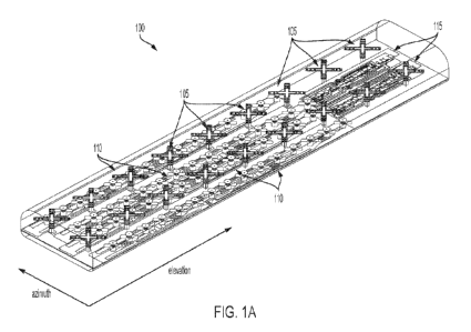
[3] Accommodating CBRS in existing LTE and 5G cellular networks requires
enhancing
antennas to operate in 3550-3700 MHz, in addition to LTE low band (LB) and
(now mid) bands
(MB) in the range of 700 MHz and 2.3 GHz, respectively. A challenge arises in
integrating C-
Band or CBRS radiators into antennas designed to operate in the existing lower
bands in that
energy radiated by the C-Band radiators may cause resonances in the lower band
radiators. A
particular problem may arise in the low band radiators that are in close
proximity to the C-
Band radiators whereby the low band radiators may significantly degrade the
performance of
the antenna in the C-Band band. The same is true for low band radiators that
are in close
proximity to mid band radiators, whereby energy emitted by the mid band
radiators causes
resonance in the low band radiators, which subsequently re-radiates to
interfere with the mid
band radiators radiation patterns.
[4] A conventional solution is to increase the area of the array face to
accommodate
1
CA 03178891 2022- 11- 15
WO 2021/230922
PCT/ITS2021/012420
additional radiators and avoid re-radiation and other forms of interference.
This is generally
not practical because increasing the area of the antenna exacerbates wind
loading, which can
have severe consequences with multiple antennas deployed on tall cell towers.
Further, given
limited space availability on a given cell tower, or in a typical urban
deployment, it is generally
not feasible to simply increase the size of the antenna.
[5] Accordingly, what is needed is a low band radiator design
that prevents re-radiation in
the mid band and CBRS bands, thus enabling the low band radiators to be placed
in close
proximity to the mid band and CBRS radiators, thereby enabling the packing of
radiators of
multiple bands into a smaller antenna array face.
SUMMARY OF THE INVENTION
[61 An aspect of the present invention involves an antenna. The
antenna comprises a
plurality of low band radiators, and a plurality of mid band radiators. Each
of the plurality of
low band radiators includes a plurality of low band dipole arms, wherein each
of the plurality
of low band dipole arms has a two-dimentional structure and inclues an
alternating sequence
of capacitive choke segments and inductive choke segments, and wherein each of
the low band
dipole arms has a broken peripheral current path.
[7] Another aspect of the present invention involves an
antenna. The antenna comprises a
plurality of mid band radiators; a plurality of high band radiators; and a
plurality of low band
radiators, wherein the plurality of low band radiators includes a first subset
of low band
radiators that are in close proximity to one or more of the plurality of mid
band radiators and a
second subset of low band radiators that are in close proximity to one or more
of the plurality
of high band radiators, wherein each of the low band radiators includes a
plurality of low band
dipole arms, each of the low band dipole arms having a central conductor, a
mantle disposed
on an outer surface of the central conductor, and a conductive pattern
disposed on an outer
2
CA 03178891 2022- 11- 15
WO 2021/230922
PCT/ITS2021/012420
surface of the mantle. werein the low band radiators in the first subset of
low band radiators
have a first conductive pattern, and the low band radiators in the second
subset of low band
radiators have a second conductive pattern, wherein the first conductive
pattern is different
from the second conductive pattern, wherein the first conductive pattern is
configured to
prevent a mid band re-radiation and the second conductive pattern is
configured to prevent a
high band re-radiation.
BRIEF DESCRIPTION OF THE DRAWINGS
[8] FIG. lA illustrates a first exemplary antenna array face that includes
a plurality of low
band dipoles according to the disclosure.
[9] FIG. 1B is an overhead view of the array face of the exemplary antenna
of FIG. 1A.
[10] FIG. 1C illustrates a portion of the array face of FIG. 1B, focusing
on the portion of
the array face having two columns of C-Band radiators and low band radiators.
[11] FIG. 2 illustrates two exemplary mid band radiators according to the
disclosure.
[12] FIG. 3 illustrates three C-Band radiators according to the disclosure.
[13] FIG. 4 illustrates a second exemplary array face, in which the C-Band
radiators are
arranged in four columns for beamforming.
[14] FIG 5A illustrates a first exemplary low band radiator according to
the disclosure.
[15] FIG. 5B illustrates a low band dipole arm of the first exemplary low
band radiator of
FIG. 5A.
[16] FIG. 5C is a drawing of the low band dipole arm of FIG. 5B, including
example
dimensions.
[17] FIG. 6A illustrates a second exemplary low band radiator, which is
configured for
cloaking mid-band RF energy, according to the disclosure.
[18] FIG. 6B illustrates a low band dipole arm of the second exemplary low
band radiator
3
CA 03178891 2022- 11- 15
WO 2021/230922
PCT/ITS2021/012420
of FIG. 6A.
[19] FIGs. 6C, 6D, and 6E provide exemplary dimensions for the low band
dipole arm
illustrated in FIG. 6B.
[20] FIG. 7A illustrates a third exemplary low band radiator, which is
configured for
cloaking C-Band RF energy, according to the disclosure.
[21] FIG. 7B illustrates a low band dipole arm of the third exemplary low
band radiator of
FIG. 7A.
DESCRIPTION OF EXEMPLARY EMBODIMENTS
[22] FIG. lA illustrates an exemplary array face 100 according to a first
embodiment of the
disclosure. Array face 100 has a plurality of low band radiators 105 (for
example, 617-960
MHz) that are arranged in two columns along the elevation axis of the antenna;
a plurality of
mid band radiators 110 (for example, 1.695-2.7 GHz) that are arranged in four
columns and
only extend for a portion of the antenna length along the elevation axis; and
a plurality of C-
Band radiators 115 (for example, 3.4-4.2 GHz) (as used herein, the C-B and
radiators may be
referred to as high band radiators) that are arranged in two columns along a
remaining length
array face 100 along the elevation axis. Each of the low band radiators 105,
mid band radiators
110, and C-Band radiators 115 comprise two orthogonal radiator arms, each of
which radiate
in a single polarization. Accordingly, each of the radiators illustrated may
operate
independently in two orthogonal polarizations ("dual polarized"), for example,
in +1-45 degree
orientations. Array face 100 may correspond to a 16 port antenna, in which the
low band
radiators 105 are given four ports one per polarization per column; the mid
band radiators 110
are given eight ports: one per polarization per column; and the C-Band
radiators 115 are given
four ports: one per polarization per column.
[23] FIG. 1B is an overhead view of array face 100, providing further
detail regarding the
4
CA 03178891 2022- 11- 15
WO 2021/230922
PCT/ITS2021/012420
placement of low band radiators 105, mid band radiators 110, and C-Band
radiators 115. And
FIG. 1C is a close-up view of the illustration of FIG. 1B, focusing on the two
columns of C-
Band radiators 115 and the two columns of low band radiators 105 that are in
close proximity
thereto. It will be readily apparent that the low band radiators 105 are
placed very close to mid
band radiators 110 and C-Band radiators 115, respectively, such that RF
emissions from the
mid band radiators 110 and the C-Band radiators 115 would couple with non-
cloaked or
conventionally-cloaked low band radiators 105.
[24] FIG. 2 illustrates two exemplary mid band radiators 110 according to
the disclosure.
As illustrated, the mid band radiators 110 have two independent sets of
dipoles that radiate in
orthogonal polarization orientations, in this case +1-45 degrees.
[25] FIG. 3 illustrates a portion of one column of C-Band radiators 115
according to the
disclosure. As with the mid band radiators 110, each of the C-Band radiators
115 has two
independent sets of dipoles that radiate in orthogonal polarization
orientations, in this case +/-
45 degrees. It will be understood that the C-Band radiators 115 may operate in
the CBRS
channels.
[26] Although the low band radiators 105, mid band radiators 110, and C-B
and radiators
115 are described as radiating in +/-45 degrees orientations, it will be
understood that each of
the low band radiators 105, mid band radiators 110, and C-Band radiators 115
may be fed
signals so that they radiate in a circular polarized fashion.
[27] FIG. 4 illustrates a second exemplary array face 400, in which the C-B
and radiators
115 are arranged in four columns that are substantially 2/2 apart between
them, which may
accommodate C-Band beamforming. Array face 400 has two columns of low band
radiators
105 and four columns of mid band radiators 110. As with array face 100,
certain low band
radiators 105 are in close proximity to and shadow the mid band radiators 110,
and the
remaining low band radiators 105 are in close proximity to and shadow at least
some of the C-
CA 03178891 2022- 11- 15
WO 2021/230922
PCT/ITS2021/012420
Band radiators 115. Accordingly, array face 400 may be deployed in a 20 port
antenna.
[28] A problem common to array faces 100 and 400, which would be endemic to
any array
face having conventional low band radiators in close proximity to mid band 110
or C-Band
radiators 115, is that energy respectively radiated by the mid band radiators
110 and C-band
radiators 115 imparts the flow of current within the dipoles of a conventional
low band radiator
that intersects the gain pattern of transmitting radiator 110/115. The current
generated within
the dipoles of the conventional low band radiator in turn re-radiates, thereby
interfering with
the gain pattern of the transmitting radiator 110/115. The use of cloaking in
low band radiators
is known. However, conventional cloaking can lead to two tradeoff factors: it
may increase the
complexity and cost of manufacturing the low band radiator; and the cloaking
may not be
equally effective across the bands of the transmitting radiators 110/115.
[29] FIG. 5A illustrates a low band radiator 505 that may be used is the
low band radiators
105 for array faces 100 and 400. Low band radiator 505 has a plurality of
dipoles 550 that are
mechanically coupled to balun stem 565, which has feed lines that provide RF
energy to ¨ and
receive RF energy from ¨ dipoles 550. Low band radiator 505 may also have a
passive radiator
555, which can be used to adjust the bandwidth of low band radiator 505 and
adjust its
directivity, and a passive support structure 560. The advantage of low band
radiator 505 is that
it is simple and easy to manufacture because dipoles 550 may be formed of a
stamped sheet
metal. Further, the design of dipoles provide a good compromise in ease of
manufacture with
good cloaking performance in both the mid band and C-Band.
[30] FIG. 5B illustrates an exemplary dipole arm 550 of low band radiator
505. Dipole arm
550 has an alternating sequence of capacitive choke segments 575 and inductive
choke
segments 570. An important feature of dipole arm 550 is that it does not have
a continuous
conductive trace running along its length, but is interrupted by the
alternation of capacitive
choke segments 575 and inductive choke segments 570. Dipole arm 550 has a two
dimensional
6
CA 03178891 2022- 11- 15
WO 2021/230922
PCT/ITS2021/012420
structure, which may mean that it is defined by a pattern that may be stamped
out of sheet metal
or printed on a circuit board without layering of components (other than a
printed trace on a
circuit board). Dipole arm 550 may be stamped aluminum or brass, or may be
implemented on
a printed circuit board using FR4, for example. It will be understood that
such variations are
possible and within the scope of the disclosure.
[31] FIG. 5C provides example dimensions for dipole arm 550.
[32] FIG. 6A illustrates an exemplary low band radiator 605, which may be
used as a low
band radiator 105 in array face 100/400 for those low band radiators 105 that
are in close
proximity to the mid band radiators 110. In other words, low band radiator 605
has cloaking
structure that is optimized for preventing re-radiation in the mid band
frequencies. Low band
radiator 605 has a plurality of dipole arms 650, which are coupled to a balun
stem 665, and
may have a passive radiator 655, which can be used to adjust the bandwidth of
low band
radiator 605 and adjust its directivity.
[33] FIG. 6B illustrates an exemplary low band dipole arm 650 according to
the disclosure.
Low band dipole arm 650 is designed to prevent re-radiation in the mid band.
Low band dipole
arm 650 has a center conductor tube 670, which is surrounded by a mantle 675.
Center
conductor tube 670 may be a tin-plated aluminum tube. Mantle 675 may be formed
of a
dielectric material, such as Teflon, or Delrin 100AF, although other materials
with similar
dielectric properties may be used. Disposed on the outer surface of mantle 675
is a conductive
pattern 680. Conductive pattern 680 may have dimensions and features that make
the dipole
arm 650 transparent to mid band RF energy radiated by the mid band radiators
110 whereby
mid band RF energy percolates through the mantle 675 and radiates outward
according to the
corresponding to the mid band radiator's 110 gain pattern, substantially
undisturbed by the
presence of low band dipole arm 650. In other words, the presence of
conductive pattern 680
renders low band dipole arm 650 effectively transparent to mid band RF energy.
Further, low
7
CA 03178891 2022- 11- 15
WO 2021/230922
PCT/US2021/012420
band dipole arm 650 has a broken peripheral current patch, which means that
there is not a
single straight conductive path along the outer edges of low band dipole arm
650.
[34] FIGs. 6C, 6D, and 6E provide exemplary dimensions (in inches) for low
band dipole
arm 650.
[35] FIG. 7A illustrates an exemplar low band radiator 705, which may be
used as a low
band radiator 105 in array face 100/400 for those low band radiators 105 that
are in close
proximity to the C-Band radiators 115. In other words, low band radiator 705
has a cloaking
structure that is optimized for preventing re-radiation in the C-Band
frequencies. Low band
radiator 705 has a plurality of dipole arms 750, which are coupled to a balun
stem 765. Low
band radiator 705 may have a passive radiator 755, which can be used to adjust
the bandwidth
of low band radiator 705 and adjust its directivity.
[36] FIG. 7B illustrates an exemplary low band dipole arm 750, which is
designed to
prevent re-radiation in the C-B and. Low band dipole arm 750 has a center
conducting rod 770,
which is surrounded by a mantle 775. The center conducting rod 770 and mantle
775 may be
substantially similar to the corresponding components of low band dipole 650.
Disposed on the
outer surface of mantle 775 is a conductive pattern, which may comprise a
plurality of
conductive swirl patterns 780. The presence of the conductive swirl patterns
780 on the outer
surface of mantle 775 inhibits re-radiation of C-Band radiation in low band
dipole arm 750
such that C-Band RF energy emitted by nearby C-Band radiators 115 effectively
percolates
through the mantle 775 and continues substantially undisturbed according to
its gain pattern.
8
CA 03178891 2022- 11- 15