Note: Descriptions are shown in the official language in which they were submitted.
Attorney Docket No. P1 0960CA00
DEVICES TO MITIGATE POLARIZATION MODE DISPERSION
BACKGROUND
[00011 Optical receivers for telecommunication systems, and the like, are
generally
configured to receive optical signals that have a random polarization, such
that symbols
(e.g. binary data) may be encoded on one, or both, of a TE (transverse
electric)
polarization mode or a TM (transverse magnetic) polarization mode. However,
between
an input coupler and an optical detector at the optical receiver, the
polarization modes
of the optical signal may travel at different rates (e.g. the TE polarization
mode may
travel slower than the TM polarization mode), and hence a time delay may be
introduced between the polarization modes. Such a time delay may cause the TE
and
TM polarization modes to arrive at the optical detector at different times,
which may
lead to intersymbol interference and hence errors in detecting the optical
signal.
BRIEF DESCRIPTION OF THE SEVERAL VIEWS OF THE DRAWINGS
[00021 For a better understanding of the various examples described herein and
to show
more clearly how they may be carried into effect, reference will now be made,
by way
of example only, to the accompanying drawings in which:
100031 FIG. 1 is a device to mitigate polarization mode dispersion, in
accordance with
some examples.
10004] FIG. 2 is another device to mitigate polarization mode dispersion, in
accordance
with some examples.
100051 Skilled artisans will appreciate that elements in the figures are
illustrated for
simplicity and clarity and have not necessarily been drawn to scale. For
example, the
dimensions of some of the elements in the figures may be exaggerated relative
to other
elements to help to improve understanding of embodiments of the present
invention.
10006] The apparatus and method components have been represented where
appropriate by conventional symbols in the drawings, showing only those
specific
details that are pertinent to understanding the embodiments of the present
invention so
Date Recue/Date Received 2022-11-02
Attorney Docket No. P1 0960CA00
as not to obscure the disclosure with details that will be readily apparent to
those of
ordinary skill in the art having the benefit of the description herein.
2
Date Regue/Date Received 2022-11-02
Attorney Docket No. P10960CA00
DETAILED DESCRIPTION
[00071 Optical receivers for telecommunication systems, and the like, are
generally
configured to receive optical signals that have a random polarization, such
that symbols
(e.g. binary data) may be encoded on one, or both, of a TE (transverse
electric)
polarization mode or a TM (transverse magnetic) polarization mode. However,
between
an input coupler and an optical detector at the optical receiver, the
polarization modes
of the optical signal may travel at different rates (e.g. the TE polarization
mode may
travel slower than the TM polarization mode), a phenomenon known as
polarization
mode dispersion, and hence a time delay may be introduced between the
polarization
modes. Such a time delay may cause the TE and TM polarization modes to arrive
at the
optical detector at different times, which may lead to intersymbol
interference and
hence errors in detecting the optical signal.
[9008I For example, the optical detector is understood to detects intensity of
the optical
signal and does not distinguish between polarization modes. Hence when a "1"
and an
adjacent "0", for example in an order of "1" followed by "0", are encoded on
both the
TE and TM polarization modes, for example as different intensity levels, and
the "0"
encoded in the TM polarization mode arrives at the optical detector the same
time as
the "1" encoded in the TE polarization mode (e.g. the "1" encoded in the TM
polarization mode having previously arrived at the optical detector), the
optical detector
will generally detect an intensity corresponding to a value between "0" and
"1" (e.g as
the optical detector detects an intensity that is the sum of the TE and TM
polarization
modes), leading to an error in detection known as intersymbol interference.
1.00091 In particular, polarization mode dispersion may be acute in photonic
integrated
circuits (PlCs) comprising, for example, silicon-on-insulator (SOT) devices.
[0010] Hence, provided herein is a device, and in particular an optical
receiver, which
receives an optical signal comprising a first portion in a first polarization
mode (e.g. a
TE polarization mode) and a second portion in a second polarization mode (e.g.
a TM
polarization mode), perpendicular to the first polarization mode. As the
optical signal
arrives at the device, there may be no polarization mode dispersion and/or
minimal
polarization mode dispersion such that encoding on both the polarization modes
is
3
Date Recue/Date Received 2022-11-02
Attorney Docket No. P1 0960CA00
aligned. The device includes an input coupler and an optical detector, such as
a
photodiode, and the device is generally configured to convey the optical
signal from
the input coupler to the optical detector for detection. The first and second
polarization
modes are understood to travel through the device at different rates (e.g. the
aforementioned polarization mode dispersion). For example, the TE polarization
mode
may travel through SOI PIC devices slower than the TM polarization mode.
[0011] As such, the device includes a rotating component configured to rotate
the first
polarization mode of the first portion to the second polarization mode, and
rotate the
second polarization mode of the second portion to the first polarization mode,
to adjust
a total differential group delay between the portions. For example, as the
first portion
is conveyed through the device in the first polarization mode and then is
inverted and/or
rotated by the rotating component to the second polarization mode, and as the
second
portion is conveyed through the device in the second polarization mode and
then is
inverted and/or rotated by the rotating component to the first polarization
mode, a total
differential group delay between the first portion and the second portion may
be
adjusted due to the rotation.
[00121 In particular, a differential group delay between the polarization
modes may
initially be zero upon entering the input coupler. The term "differential
group delay" as
used herein is understood to refer to a relative delay between the first
portion and the
second portion introduced by respective components of the device through which
the
optical signal is conveyed; hence a given differential group delay may be for
a particular
component of the device. Furthermore, the term "total differential group
delay" as used
herein is understood to refer to a total difference in differential group
delay between the
first portion and the second portion introduced by all the components of the
device
through which the optical signal is conveyed. Hence, a total differential
group delay
may comprise a sum of respective differential group delays of all the
components of
the device through which the optical signal is conveyed.
100131 Furthermore, units for differential group delays and/or total
differential group
delays may be on the order of microseconds and/or nanoseconds, and the like,
and may
be relative to an initially faster portion of an optical signal. For example,
if a first portion
4
Date Regue/Date Received 2022-11-02
Attorney Docket No. P10960CA00
of an optical signal is in a TE polarization mode, and a second portion of the
optical
signal is in a faster TM polarization mode, a differential group delay for the
optical
signal being conveyed through an optical component may be positive, as the
differential
group delay may comprise a value, in time, that the second portion moves ahead
of the
first portion while the optical signal is conveyed through the optical
component.
However, a differential group delay for the optical signal being conveyed
through an
optical component may be negative when the second portion is inverted to the
slower
'FE polarization mode and the first portion is inverted to the faster TM
polarization
mode, as the differential group delay, in this example, may comprise a value,
in time,
that the second portion falls behind of the first portion while the optical
signal is
conveyed through the optical component.
100141 Furthermore, the term "inverted" as used herein with respect to a
polarization
mode is understood to refer to converting a first polarization mode to a
second
polarization mode that is perpendicular to the first polarization mode. Hence,
for
example, a TE polarization mode may be inverted by a rotating component, as
provided
herein, to a TM polarization mode and, conversely, a TM polarization mode may
be
inverted by a rotating component, as provided herein, to a TE polarization
mode.
100151 In particular, as the optical signal is conveyed through the device,
for example
using optical waveguides, respective differential group delays may be
introduced
between the first polarization mode and the second polarization mode by the
input
coupler and the optical waveguides. For example, such respective differential
group
delays may be introduced by one or more of the input coupler, a first optical
waveguide
from the input coupler to the rotating component and a second optical
waveguide from
the rotating component to the optical detector, as well as the rotating
component.
However, the optical waveguides may be optional, and respective differential
group
delays may be introduced primarily by the input coupler and the rotating
component.
Indeed, each respective component of the device, through which the optical
signal is
conveyed, may introduce a respective differential group delay; furthermore,
the rotating
component rotates and/or inverts the polarization modes of the two portions of
the
optical signal, and introduces a respective differential group delay
therebetween to
Date Recue/Date Received 2022-11-02
Attorney Docket No. P1 0960CA00
compensate for the differential group delays of the other components of the
device
through which the optical signal is conveyed. For example, if the first
portion in the
first polarization mode is initially slower than the second portion in the
second
polarization mode, after the rotating component, the first portion in the
second
polarization mode is faster than the second portion in the first polarization
mode. As
such, the rotating component may invert the differential group delay between
the first
portion and the second portion so that the total differential group delay, as
the first
portion and the second portion enters the optical detector, is zero, and/or a
given value.
[0016] In some examples, the rotating component comprises a polarization
rotator
which is located at a position in the device, relative to the input coupler
and the optical
detector, selected to adjust the total differential group delay to about zero,
and/or to a
given value, in combination with the rotating component rotating the
polarization
modes. The location of the rotating component may be selected by selecting
respective
lengths of a first optical waveguide from the input coupler to the rotating
component
and a second optical waveguide from the rotating component to the optical
detector.
Put another way, the rotating component is located at a position at the device
such that
both the portions of the optical signal are conveyed through the device
partially in a
first, slower, polarization mode and partially in a second, faster,
polarization mode, such
that the differential group delays between the portions balance to about zero
and/or to
a given value.
[0017I In other examples, the rotating component may comprise a pair of
polarization
splitter rotators that are joined by a pair of intermediate optical wavegu
ides of different
lengths. A first polarization splitter rotator splits the optical signal into
two portions
having respective polarization modes (e.g. TE and TM polarization modes). The
first
polarization splitter rotator further rotates a polarization mode of one of
the two portions
into the other polarization mode (e.g. the TM polarization mode is rotated to
the TE
polarization mode) so that the two portions are in the same polarization mode.
The
splitting and the rotating may occur in any suitable order and/or
concurrently. A first
portion of the optical signal, having a polarization mode that is initially
"behind" (e.g.
delayed in time) a polarization mode of a second portion, is conveyed to a
shorter
6
Date Recue/Date Received 2022-11-02
Attorney Docket No. P1 0960CA00
intermediate optical waveguicle, and the second portion, having a polarization
mode
that is initially "ahead"" (e.g. ahead in time) of a polarization mode of a
first portion,
is conveyed to a longer intermediate optical waveguides. The difference in
length
between the intermediate optical waveguides generally brings a total
differential group
delay to zero and/or to given value. A second polarization splitter rotator
receives the
Iwo portions and rotates a polarization mode of the first portion, while not
rotating the
polarization mode of the second portion; the result is that the first portion
and the second
portion are in respective polarization modes opposite to what they were upon
entering
the device. The second polarization splitter rotator further combines the
first portion
and the second portion (e.g. the rotating and combining occurring in any
suitable order).
The first portion and the second portion are conveyed to the optical detector.
As with
the polarization rotator, the combination of the PSRs and the pair of
intermediate optical
waveguides of different lengths, both invert the polarization mode of each of
the first
portion and the second portion, and introduce a differential group delay that
assists in
adjusting the total differential group delay for the device to about zero
and/or to a given
value.
[00181 An aspect of the present specification provides a device comprising: an
input
coupler configured to receive an optical signal comprising a first portion in
a first
polarization mode and a second portion in a second polarization mode, the
second
polarization mode about perpendicular to the first polarization mode; one or
more of an
output and an optical detector; and one or more optical components configured
to
convey the optical signal from the input coupler to one or more of the output
and the
optical detector, one or more of the input coupler and the one or more optical
components introducing a total differential group delay between the first
portion and
the second portion, the one or more optical components comprising: a rotating
component configured to rotate the first polarization mode of the first
portion to the
second polarization mode and rotate the second polarization mode of the second
portion
to the first polarization mode, to adjust the total differential group delay.
100191 An aspect of the present specification provides a device comprising: an
input
coupler having a first differential group delay value; a first optical
waveguide coupled
7
Date Recue/Date Received 2022-11-02
Attorney Docket No. P1 0960CA00
to the input coupler, the first optical waveguide having a second differential
group delay
value; a rotating component coupled to the first optical waveguide, the
rotating
component configured to rotate a first polarization mode to a second
polarization mode
perpendicular to the first polarization mode; and rotate the second
polarization mode to
the first polarization mode; the rotating component having a third
differential group
delay value; a second optical waveguide coupled to the rotating component, the
second
optical waveguide having a fourth differential group delay value; and one or
more of
an output and an optical detector coupled to the second optical waveguide, the
second
differential group delay value and the fourth differential group delay value
dependent
on respective lengths of the first optical waveguide and the second optical
waveguide,
the respective lengths selected such that a total differential group delay
value of the
input coupler, the first optical waveguide, the rotating component and the
second
optical waveguide is one or more of about zero and a given value.
[0020i An aspect of the present specification provides a device comprising: an
input
coupler; one or more of an output and an optical detector; a first
polarization splitter
rotator (PSR) in optical communication with the input coupler; a second PSR in
optical
conimunication with one or more of the output and the optical detector; and a
pair of
intermediate optical waveguides that optically couple the first PSR and the
second PSR,
the pair of intermediate optical waveguides being of different lengths, the
first PSR
configured to: split an optical signal from the input coupler into a first
portion having
a first polarization mode and a second portion having a second polarization
mode,
perpendicular to the first polarization mode; rotate the second polarization
mode to the
first polarization mode such that both the first portion and the second
portion are in the
first polarization mode; and convey the first portion and the second portion
to respective
optical waveguides of the pair of intermediate optical waveguides, the
different lengths
between the pair of intermediate optical waveguides adjusting a differential
group delay
between the first portion and the second portion, the second PSR configured
to: rotate
the first polarization mode of the first portion to the second polarization
mode such that
the first portion is in the second polarization mode and the second portion is
in the first
polarization mode; combine the first portion and the second portion; and
output the first
8
Date Regue/Date Received 2022-11-02
Attorney Docket No. P1 0960CA00
portion and the second portion towards one or more of the output and the
optical
detector.
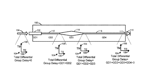
[00211 Attention is hence directed to Fig. 1 which depicts a device 100 to
mitigate
polarization mode dispersion. The device 100 generally comprises an optical
receiver
photonie integrated circuit (PIC) fabricated using SOI, however the device 100
may
comprise any suitable combination of materials.
[0022] The device 100 generally comprises an input coupler 102 configured to
receive
an optical signal 104. The input coupler 102 may be any suitable optical
component
that may adapted to receive an optical signal and may comprise a facet, and
the like, at
an edge of the device 100 and/or a coupler to an optical fiber through which
the optical
signal 104 is being conveyed to the device 100. The optical signal 104 may be
encoded
with any suitable data (e.g. in a binary format), including, but not limited
to, audio,
video, and/or any other suitable data
[00231 The optical signal 104 may comprises a first portion 106 in a first
polarization
mode and a second portion 108 in a second polarization mode, the second
polarization
mode about perpendicular to the first polarization mode. For clarity, the
portions 106,
108 are depicted adjacent the optical signal 104 in FIG, 1, which is
understood to
comprise any suitable wavelength (and/or combination thereof) which may be
compatible with optical telecommunication systems.
[0024] As the optical signal 104 enters the input coupler 102, the first
polarization mode
of the first portion 106 may comprise one of a TE (transverse electric)
polarization
mode or a TM (transverse magnetic) polarization mode, and the second
polarization
mode of the second portion 108 comprises an other of the TE polarization mode
or the
TM polarization mode. As depicted, the first polarization mode of the first
portion 106
comprises the TE polarization mode and the second polarization mode of the
second
portion 108 comprises the TM polarization mode. This example will be used
hereafter,
though it is understood that the polarization modes of the portions 106, 108
may be any
suitable polarization modes. Furthermore, for clarity, hereafter, when a
portion 106,
108 is depicted as being left to right within a drawing, such a portion 106,
108 is
understood to be in the TE polarization mode; and, similarly, hereafter, when
a portion
9
Date Recue/Date Received 2022-11-02
Attorney Docket No. P10960CA00
106, 108 is depicted as being up to down within a drawing, such a portion 106,
108 is
understood to be in the TM polarization mode.
100251 Furthermore, as depicted, the polarization modes of the portions 106,
108 are
understood to have a total differential group delay of about "0".
100261 As depicted, the device 100 further comprises one or more of an output
and an
optical detector 110 (e.g. located at the output 111), such as a photodiode,
and the like,
and one or more optical components configured to convey the optical signal 104
from
the input coupler 102 to the optical detector 110 and/or the output 111 of the
device
100. As depicted, the optical detector 110 is located at the output Ill.
[00271 However, it is understood that as the device 100 may generally comprise
a
photonics integrated circuit, the optical detector 110 may also a component of
the
photonics integrated circuit; alternatively the optical detector 110 may be
adjacent to,
but not part of the photonic integrated circuit. Hence, in some examples, PIC
portions
of the device 100, may be provided without the optical detector 100, and the
optical
detector 110 may later be placed adjacent the output I 1 1 However, in other
examples,
the optical detector 110 may be part of the PIC portions of the device 100
(e.g. the
optical detector 110 may also comprise a PIC), such that the device 100 is
provided as
a PIC which includes the optical detector 110 (e.g. located at the output 111
of the one
or more optical components configured to convey the optical signal 104 from
the input
coupler 102 towards the optical portion 110).
[00281 In general, the optical detector 110 detects intensity and/or power of
the optical
signal 104 and does not distinguish between polarization modes of the portions
106,
108. While not depicted, the optical detector 110 is generally configured to
communication with a processing device which processes output from the optical
detector 110, for example, to convert data of the optical signal 104, as
detected by the
optical detector 110, to data that may be output and/or stored, and the like.
[0029j As depicted, the one or more optical components include a first optical
waveguide 112, a rotating component 114 and a second optical waveguide 116,
however the optical waveguides 112, 116 may be optional. In particular, the
first optical
waveguide 112 optically couples the input coupler 102 to the rotating
component 114,
Date Regue/Date Received 2022-11-02
Attorney Docket No. P10960CA00
and the second optical waveguide 116 optically couples the rotating component
114 to
an output 111 at which the optical detector 110 is located. Put another way,
the second
optical waveguide 116 optically couples the rotating component 114 to one or
more of
the output 111 and the optical detector 110.
100301 In general, one or more of thc input coupler 102 and the one or more
optical
components (e.g. such as the optical waveguides 112, 116 and the rotating
component
114) introduces a total differential group delay between the first portion 106
and the
second portion 108. Put another way, all the components of the device 100
through
which the optical signal 104 travels introduce respective differential group
delays
between the portions 106, 108, with a total differential group delay
comprising a sum
of the respective differential group delays.
100311 For example, the optical signal 104 may be conveyed to the device 100
via
optical fiber. While polarization mode dispersion may not generally a problem
with
optical fiber, as the device 100 generally comprise a PIC which may be
fabricated from
SOI, the input coupler 102 and the optical waveguides 112, 116, when present,
introduce respective differential group delays between the TE and TM
polarization
modes. For example, the TE polarization mode tends to travel through SO1
slower than
the TM polarization mode, hence, without the rotating component 114,
functionality of
which is described in more detail below, a total differential group delay
between the
first portion 106 and the second portion 108 will be higher at the optical
detector 110
than when the optical signal 104 enters the input coupler 102.
100321 In particular, the rotating component 114 is generally configured to
rotate the
first polarization mode of the first portion 106 to the second polarization
mode and
rotate the second polarization mode of the second portion 108 to the first
polarization
mode, to adjust the total differential group delay. For example, as depicted,
upon exiting
the rotating component, the polarization modes of the first portion 106 and
the second
portion 108 of the optical signal 104 are rotated and/or inverted, such that
the first
portion 106 is in the TM polarization mode and the second portion 108 is in
the TE
polarization mode. Hence, put another way, the rotating component 114 is
configured
Date Recue/Date Received 2022-11-02
Attorney Docket No. P10960CA00
to invert a differential group delay between the first portion 106 and the
second portion
108.
[00331 In particular, as depicted, the input coupler 102, the first optical
waveguide 112,
the rotating component 114, and the second optical waveguide 116 respectively
introduce differential group delays (e.g. labelled "GDn" in FIG. 1 and through
the
present specification) of GD I, GD2, GD3, GD4, the labels "GDn" being adjacent
respective components of the device 100 in FIG. Ito indicate the respective
differential
group delay introduced by the components. For example, the TE mode tends to
travel
through SOI (e.g. of the input coupler 102, the optical waveguides 112, 116
and the
rotating component 114) slower than the TM mode, each of the input coupler
102, the
optical waveguides 112, 116 and the rotating component 114.
100341 In general, the differential group delay, GD3, of the rotating
component 114 is
selected such that the total differential group delay is one or more of zero
and a given
value. For example, a total differential group delay may be defined as:
100351 Total_GD = En".t GDn=Value....Equation (1)
100361 For Equation (1), Total GD comprises the total differential group
delay, and
GDn is a respective differential group delay of an nth component of the device
100
through which the optical signal 104 is conveyed, and N is the total number of
components of the device 100 through which the optical signal 104 travel.
[00371 The value, Value, to which the total differential group delay may be
set may be
zero. However, in other examples, the optical signal 104 may arrive at the
device 100
with a given differential group delay, and hence the value of the total
differential group
delay for Equation (1) may be selected to compensate for such given
differential group
delay. For example, if the given differential group delay between the portions
106, 108
is not "0" (e.g. as depicted in FIG. 1) as the optical signal 104 arrives at
the input coupler
102, but a value of "-Value", the total differential group delay of Equation
(1) may be
set to " Value".
100381 As depicted in FIG. 1, for N=4 (e.g. the components of the device 100
through
which the optical signal 104 is conveyed includes four components including
the input
Date Regue/Date Received 2022-11-02
Attorney Docket No. P10960CA00
coupler 102, the optical waveguides 112, 116 and the rotating component 114),
the total
differential group delay is:
[00391 TotalGo = GD1 GD2 GD3 GD4....Equation (2)
[00401 In general, assuming that differential group delay is defined as being
relative to
the second portion 108, and that the second portion 108 is initially in the TM
polarization mode and travelling faster through the input coupler 102 and the
first
optical waveguide 112 than the first portion 106 in the TE polarization modes,
the
differential gaup delay GD1 for the input coupler 102 and differential group
delay
GD2 for the first optical waveguide 112 are both positive (e.g. the second
portion 108
is faster than the first portion 106). A size of the differential group delays
GD I , GD2
generally depend on a length of the input coupler 102 and the first optical
waveguide
112. Put another way, the longer the input coupler 102 and/or the first
optical waveguide
112, the greater their respective differential group delays GD I, GD2. Indeed,
as
depicted, as the optical signal 104 enters the rotating component, the total
differential
group delay is CID1-4.1D2.
100411 However, as the first portion 106 and the second portion 108 have their
polarization modes inverted by the rotating component 114, such that the first
portion
106 in the TM polarization mode is travelling faster through the rotating
component
114 and the second optical waveguide 116, the differential group delay GD4 of
the
second optical waveguide 116 will generally be negative, and the differential
group
delay GD3 of the rotating component 114 may be negative and/or reduced
relative to if
the polarization modes of the portions 106, 108 were not inverted.
100421 An absolute size and/or value of the differential group delays GD3, GD4
may
generally depend on a length of the rotating component 114 and the second
optical
waveguide 116. Put another way, the longer the rotating component 114 and the
second
optical waveguide 116, the greater their respective differential group delays
GD3, GD4.
However, an absolute size and/or value of the differential group delay GD3 of
the
rotating component 114 may also depend on where, within the rotating component
114,
inversion of the polarization modes of the portions 106, 108 occurs; in
practice,
1.3
Date Recue/Date Received 2022-11-02
Attorney Docket No. P10960CA00
however, the differential group delay GD3 of the rotating component 114 may be
predetermined via a given design of the rotating component 114.
100431 In general, as the respective differential group delays GD1, GD2, GD4
of the
input coupler 102, the first optical waveguide 112 and the second optical
waveguide
116 are known and/or may be measured, a respective differential group delay
GD3 of
the rotating component 114 may be selected such that the total diffloren tial
group delay
is zero and/or a given value.
100441 Put another way, when the device 100 is being considered for
fabrication,
lengths of the input coupler 102, the first optical waveguide 112 and the
second optical
waveguide 116 may be predetermined and/or selected for optical design purposes
and/or space considerations in the device 100. Once the lengths of the input
coupler
102, the first optical waveguide 112 and the second optical waveguide 116 are
selected,
their respective differential group delays GD1, GD2, GD4 may be determined,
for
example as SOT devices, and the like, may generally have well understood
and/or
predetermined properties such that the polarization mode dispersion of SOT
devices,
and the like, may be determined.
100451 As such, the respective differential group delay GD3 of the rotating
component
114 may be selected such that the total differential group delay is zero
and/or any other
suitable predefined value. In particular, Equation (2) may be adapted to:
[0046] TotalGD = GD1 + GD2 + GD3 + GD4 = Vatue....Equation (3)
[0047] In Equation (3), Value is any suitable given value for the total
differential group
delay which may include, but is not limited to zero.
[0048] Hence, for example, the respective differential group delay GD3 of the
rotating
component 114 may he selected using the given value, Value, and the respective
differential group delays GDI, GD2, GD4 of the input coupler 102, the first
optical
waveguide 112 and the second optical waveguide 116 as follows:
[0049] GD3 = Value ¨ (GD1 + GD2 + GD4).. Equation (4)
[0050] Alternatively, the differential group delay GD3 of the rotating
component 114
may be fixed but of a size that may adjust the total differential group delay
to zero
and/or the given value, Value, presuming the respective differential group
delays GD2,
14
Date Recue/Date Received 2022-11-02
Attorney Docket No. P10960CA00
GD4 of the optical waveguides 112, 116 may be adjusted, for example by
adjusting one
or more of their respective lengths, by:
[0051] GD2 + GD4 = Value ¨ (GD1 + GD3)...Equation (5)
[00521 Hence, given fixed and/or predetermined values for the respective
differential
group delays GD I , GD3 of the input coupler 102 and the rotating component
114, a
subtotal (e.g. CTD2+GD4) of the differential group delays GD2, GD4 of the
optical
waveguides 112, 116 and their lengths selected accordingly.
[00531 Regardless, as depicted, it is understood that the total differential
group delay of
the portions 106, 108 is GD I GD2+GD3 as the optical signal 104 exits the
rotating
component 11.4, and that the total differential group delay of the portions
106, 108 is
GD I --I-GD2+GD34-GD4 as the optical signal 104 exits the output 111 and/or
enters the
optical detector 110. In some examples, as depicted, the total differential
group delay
of the portions 106, 108 of GD1-FGD2H-GD3+GD4 as the optical signal 104 exits
the
output 111 and/or enters the optical detector 110 may be "0" and/or about "0".
100541 Hence, it is generally understood that device 100 comprises: the input
coupler
102 configured to receive the optical signal 104 comprising the first portion
106 in the
first polarization mode and the second portion 108 in the second polarization
mode, the
second polarization mode about perpendicular to the first polarization mode;
one or
more of an output 111 and an optical detector 110; and one or more optical
components
configured to convey the optical signal from the input coupler 102 to one or
more of
the output 111 and the optical detector 110, one or more of the input coupler
102 and
the one or more optical components introducing a total differential group
delay between
the first portion and the second portion, the one or more optical components
comprising: the rotating component 114 configured to rotate the first
polarization mode
of the first portion 106 to the second polarization mode and rotate the second
polarization mode of the second portion 108 to the first polarization mode, to
adjust the
total differential group delay. For example, the rotating component 114 may be
configured to rotate the first polarization mode of the first portion 106 to
the second
polarization mode and rotate the second polarization mode of the second
portion 108 to
Date Regue/Date Received 2022-11-02
Attorney Docket No. P10960CA00
the first polarization mode, to adjust the total differential group delay to
one or more of
zero and a predetermined value.
100551 While the one or more optical components may further comprise one or
more
of the optical waveguides 112, 11.6, one or more of the optical waveguides
112, 116
may be optional. For example, when the first optical waveguide 112 is not
present at
the device 100, an input to the rotating component 114 is adjacent to, and
optically
coupled to, an output of the input coupler 102. Similarly, when the second
optical
waveguide 116 is not present at the device 100, an output of the rotating
component
114 is adjacent to, and optically coupled to, the output 111 of the device 100
and/or the
optical detector 110.
100561 Put another way, when the optical waveguides 112, 116 are present, it
is
understood that the device 100 may generally comprise: the input coupler 102
having a
first differential group delay value GD1, the first optical waveguide 112
coupled to the
input coupler 102, the first optical waveguide 112 having a second
differential group
delay value GD2; the rotating component 114 coupled to the first optical
waveguide
112, the rotating component 114 configured to: rotate the first polarization
mode to the
second polarization mode perpendicular to the first polarization mode; and
rotate the
second polarization mode to the first polarization mode; the rotating
component 114
having a third differential group delay value GD3; the second optical
waveguide 116
coupled to the rotating component 114, the second optical waveguide 116 having
a
fourth differential group delay value GD4; and one or more of the output I 11
and the
optical detector 1.10 coupled to the second optical waveguide 116. It is
further
understood that the second differential group delay value GD2 and the fourth
differential group delay value GD4 are generally dependent on respective
lengths of the
first optical waveguide 112 and the second optical waveguide 116, the
respective
lengths selected such that a total differential group delay value of the input
coupler 102,
the first optical waveguide 112, the rotating component 114 and the second
optical
waveguide 116 is one or more of about zero and a given value.
100571 The rotating component 114 may have any suitable configuration.
16
Date Regue/Date Received 2022-11-02
Attorney Docket No. P10960CA00
100581 For example, the rotating component 114 may comprise a polarization
rotator,
which is an optical device that rotates given polarization modes. In
particular, such a
polarization rotator rotates the respective polarization modes by 900. Hence,
for
example, such a polarization rotator rotates (e.g. inverts) the TE
polarization mode to
the TM polarization mode, and rotates (e.g. inverts) the TM polarization mode
to the
TE polarization mode.
[00591 Hence, put another way, in particular examples, the rotating component
114
may comprise a polarization rotator and the one or more optical components of
the
device 100 may further comprise: respective optical waveguides 112, 11.6
between the
rotating component I 14 and the input coupler 102, and between the rotating
component
114 and one or more of the output 111 and the optical detector 110, wherein
lengths of
the respective optical waveguides 112, 116 are selected to adjust the total
differential
group delay to one or more of about zero, and a given value, in combination
with the
rotating component 114 rotating the first polarization mode and the second
polarization
mode. Put another way, one or more of the optical waveguides 112, 116 may be
optional, however, when present, their lengths are selected such that their
respective
differential group delays GD2, GD4, in combination with the differential group
delay
GD1 of the input coupler 102 and the differential group delay GD3 of the
rotating
component 114, adjust the total differential group delay to one or more of
about zero,
and a given value.
100601 However, in other examples, the rotating component 114 may have other
configurations. For example, attention is next directed to FIG. 2 which
depicts another
example of the device 100, with the rotating component 114 adapted to include
polarization splitter rotators (PSRs) and intermediate optical waveguides
therebetween.
The device 100 is otherwise similar to as depicted in FIG. 1, with like
components
having like numbers. Again, one or more of the optical waveguides 112, 116,
while
present in FIG. 2, may be optional.
100611 In particular, as depicted in FIG. 2, the rotating component 114
comprises: a
first polarization splitter rotator (PSR) 200 in optical communication with
the input
coupler 102 and a second PSR 202 in optical communication with the output 111
and/or
17
Date Regue/Date Received 2022-11-02
Attorney Docket No. P10960CA00
the optical detector 110. As depicted, the first PSR 200 is in optical
communication
with the input coupler 102 via the first optical waveguide 112, and the second
PSR 202
in optical communication with the output 111 and/or the optical detector 110
via the
second optical waveguide 116.
100621 As depicted, the device 100 further comprises: a pair of intermediate
optical
waveguides 204, 206 that optically couple the first PSR 200 and the second PSR
202,
the pair of intermediate optical waveguides 204, 206 being of different
lengths. For
example, as depicted, a first intermediate optical waveguide 204 is shorter
than a second
intermediate optical waveguide 206. The optical waveguides 204, 206 are
referred to
herein as being "intermediate" optical waveguides 204, 206, to both
distinguish the
intermediate optical waveguides 204, 206 from the first optical waveguide 112
and the
second optical waveguide 116, and as the intermediate optical waveguides 204,
206 are
intermediate, and/or between, the PSRs 200, 202.
[00631 In general, the first PSR 200 is configured to: split the optical
signal 104 into
the first portion 106 and the second portion 108; rotate the second
polarization mode to
the first polarization mode such that both the first portion 106 and the
second portion
108 are in the first polarization mode; and convey the first portion 106 and
the second
portion 108 to respective optical waveguides 204,206 of the pair of
intermediate optical
waveguides204, 206, the different lengths of the pair of intermediate optical
waveguides 204, 206 adjusting a differential group delay between the first
portion 106
and the second portion 108. While such splitting and rotating are described in
given
order, the rotating may occur before the splitting, or the splitting may occur
before the
rotating; put another way, the functionality of the first PSR 200 may occur in
any
suitable order.
[00641 In general, the first PSR 200 conveys the portion 106, 108 having the
polarization mode that is conveyed slowest through the device 100 (e.g. up to
the
rotating component 114), to the shorter of the intermediate optical waveguides
204, 206
(e.g. the first intermediate optical waveguide 204), and the first PSR 200
further
conveys the portion 106, 108 having the polarization mode that is conveyed
fastest
through the device 100 (e.g. up to the rotating component 114), to the longer
of the
Date Regue/Date Received 2022-11-02
Attorney Docket No. P10960CA00
intermediate optical waveguides 204, 206 (e.g. the second intermediate optical
waveguide 204). Hence, as depicted, the first portion 106, in the slower FE
polarization
mode, is conveyed to the first (e.g. shorter) intermediate optical waveguide
204; the
second portion 108, which was originally in the faster TM polarization mode,
but has
been converted to the slower FE polarization mode by the first PSR 200, is
conveyed
to the second (e.g. longer) intermediate optical waveguide 204. As such, the
differential
group delay, GD3, between the first portion 106 and the second portion 108 is
reduced,
relative to the differential group delay between the first portion 106 and the
second
portion 108 as they entered the rotating component 1.14.
[00651 It is further understood that while for clarity the first portion 106
and the second
portion 108 are depicted as adjacent respective intermediate optical
waveguides 204,
206, the first portion 106 and the second portion 108 are travelling through
the
respective intermediate optical waveguides 204, 206.
[0066] Furthermore, the portions 106, 108 are understood to be in a same
polarization
mode within the intermediate optical waveguides 204, 206, and in particular in
the FE
polarization mode.
[0067] The second PSR 202 is generally configured to: rotate the first
polarization
mode of the first portion 106 to the second polarization mode such that the
first portion
106 is in the second polarization mode and the second portion 108 is in the
first
polarization mode; combine the first portion 106 and the second portion 108;
and output
the first portion 106 and the second portion 108 towards one or more of the
output Ill
and the optical detector 110, for example via the second optical waveguide
116. While
such combining and rotating are described in given order, the rotating may
occur before
the combining, or combining may occur before the rotating; put another way,
the
functionality of the second PSR 202 may occur in any suitable order.
[00681 Furthermore, while the second PSR 202 combines, and does not split, the
portions 106, 108, the second PSR 202 is still referred to as a polarization
"splitter"
rotator as polarization splitter rotators generally split optical signals into
respective
polarization modes when the optical signals travel through the polarization
splitter
rotators in a first direction (e.g. as with the first PSR 200), but
polarization splitter
19
Date Recue/Date Received 2022-11-02
Attorney Docket No. P10960CA00
rotators combine separated polarization modes into one optical signal when
travelling
through the polarization splitter rotators in a second direction opposite the
first
direction. Hence, it is understood that the PSRs 200, 202 may comprise a same
type of
device, but the first PSR 200 is oriented relative to the first optical
waveguide 112 and
the pair of intermediate optical waveguides 204, 206 such that the first PSR
200 splits
the optical signal 104 in the portions 106, 108, and the second PSR 202 is
oriented
relative to the pair of intermediate optical waveguides 204, 206 and the
second optical
waveguide 116 and such that the second PSR 202 combines the portions 106, 108
back
into a combined optical signal 104.
[0001 Hence, in general, the second PSR 202 operates in reverse fashion
relative to
the first PSR 200, such that the optical signal 104, when output from the
second PSR
202, is in a similar state as when output from the rotating component 114 as
depicted
in FIG. 1.
[00701 Furthermore, the total differential group delay of the device 100 as
depicted in
FIG. 2 is determined in a manner similar to as described with respect to the
device 100
as depicted in FIG. 1. In particular the input coupler 102, the first optical
waveguide
112, the rotating component 114 and the second optical waveguide 116 have
respective
differential group delays GD1, GD2, GD3, GD4, and Equation (1) and/or Equation
(2)
and/or Equation (3) and/or Equation (4) and/or Equation (5) may be used to
select
lengths of one or more of the optical waveguides 112, 116 and/or to select
lengths of
one or more of the intermediate optical waveguides 204, 206. In particular,
while
Equation (1), Equation (2), Equation (3), Equation (4), and Equation (5) are
directed
towards determining a total differential group delay and/or respective
differential group
delays, once a total differential group delay and/or respective differential
group delays
are determined, respective lengths of one or more of the optical waveguides
112, 116
and/or to select lengths of one or more of the intermediate optical waveguides
204, 206
may be determined based, for example, on relative speeds of the respective
polarization
modes through the device 100.
[00711 Furthermore, while the optical waveguides 112, 116 may be optional, the
device
100 may further comprise: the respective optical waveguides 112, 116 between
the
Date Recue/Date Received 2022-11-02
Attorney Docket No. P10960CA00
rotating component 114 and the input coupler 102, and between the rotating
component
114 and the optical detector 110 and/or the output 111, and the different
lengths of the
intermediate optical waveguides 204, 206 may be selected to adjust the total
differential
group delay to one or more of zero and a given value in combination with
lengths of
the respective optical waveguides112, 114.
100721 Hence, put another way, in some examples the device 100 may comprise:
the
input coupler; one or more of the output 111 and the optical detector 110; the
first PSR
200 in optical communication with the input coupler 102; the second PSR 202 in
optical
communication with the output Ill; and a pair of intermediate optical
waveguides 204,
206 that optically couple the first PSR 200 and the second PSR 202, the pair
of
intermediate optical wavegu ides 204, 206 being of different lengths. The
first PSR 200
is configured to: split the optical signal 104 from the input coupler 102 into
the first
portion 106 having a first polarization mode and the second portion 108 having
a second
polarization mode, perpendicular to the first polarization mode; rotate the
second
polarization mode to the first polarization mode such that both the first
portion 106 and
the second portion 108 are in the first polarization mode; and convey the
first portion
106 and the second portion 108 to respective optical waveguides 204, 206 of
the pair
of intermediate optical waveguides 204, 206, the different lengths between the
pair of
intermediate optical waveguides 204, 206 adjusting a differential group delay
between
the first portion 106 and the second portion 108. The second PSR 202 is
configured to:
rotate the first polarization mode of the first portion 106 to the second
polarization mode
such that the first portion 106 is in the second polarization mode and the
second portion
108 is in the first polarization mode; combine the first portion 106 and the
second
portion 108; and output the first portion 106 and the second portion 108
towards one or
more of the output 111 and the optical detector 110.
[00731 In such examples, the device 100 may further comprise: the first
optical
waveguide 112 optically coupling the input coupler 102 to the first PSR 200;
and the
second optical waveguide 116 optically coupling the second PSR 202 to the
output 111
and/or the optical detector 110.
21
Date Regue/Date Received 2022-11-02
Attorney Docket No. P10960CA00
100741 Furthermore, one or more of the input coupler 102, the first optical
waveguide
112, the second optical waveguide 116, the first PSR 200 and the second PSR
202 are
understood to introduce respective differential group delays between the first
portion
106 and the second portion 108, a respective differential group delay of the
pair of
intermediate optical waveguides 204, 206, due to the different lengths,
compensating
for the respective differential group delays such that a total differential
group delay is
one or more of about zero and a given value. Put another way, while in FIG. 2,
the
rotating component 114 is depicted as having a respective differential group
delay GD3,
such a respective differential group delay GD3 is understood to include a sum
of the
differential group delays of each of the PSRs 200, 202, and a respective
differential
group delay of the pair of the intermediate optical waveguides 204, 206.
Indeed, in these
examples, each of the PSRs 200, 202, and the pair of the intermediate optical
waveguides 204, 206, may treated as separate components through which the
optical
signal 104 is conveyed, such that, for Equation (I), N=6 and differential
group delays
for each of the input coupler 102, the optical waveguides 112, 116, the PSRs
200, 202,
and the pair of the pair of the intermediate optical waveguides 204, 206 (e.g.
six
components) are used for Equation (1).
100751 It is further understood that, while herein the effect of the rotating
component
114 on total differential group delay has been described, the rotating
component 114
may also effect polarization dependent loss (PDL) of the first portion 106 and
the
second portion 108. For example, the TM polarization mode is generally more
lossy
than the TE polarization mode. Put another way, as a portion 106, 108 of the
optical
signal 104 that is in the TM polarization mode is conveyed through the device
100, a
signal strength (e.g. power) of the portion 106, 108 may be reduced relative
to the
portion 106, 108 of the optical signal 104 that is in the TE polarization
mode. However,
as provided herein, the portions 106, 108 have their respective polarization
modes
inverted such that the first portion 106 may be conveyed though the device 100
partly
in the TE polarization mode and partly in the TM polarization mode; similarly,
the
second portion 108 may be conveyed though the device 100 partly in the TM
polarization mode and partly in the TE polarization mode. Hence, in some
examples,
22
Date Recue/Date Received 2022-11-02
Attorney Docket No. P10960CA00
lengths of one or more of the optical waveguides 112, 116 and/or one or more
of the
intermediate optical waveguides 204, 206 may be selected such that the
portions 106,
108 are about equally in the TE polarization mode and the TM polarization mode
as the
optical signal 104 is conveyed through the device 100,
100761 In this specification, elements may be described as "configured to"
perform one
or inure functions or "configured for" such functions. In general, an clement
that is
configured to perform or configured for performing a function is enabled to
perform
the function, or is suitable for performing the function, or is adapted to
perform the
function, or is operable to perform the function, or is otherwise capable of
performing
the function.
100771 It is understood that for the purpose of this specification, language
of "at least
one of X, Y, and Z" and "one or more of X, Y and Z" can be construed as X
only, Y
only, Z only, or any combination of two or more items X. Y, and Z (e.g., XYZ,
XY,
YZ, XZ, and the like). Similar logic can be applied for two or more items in
any
occurrence of at least one..." and "one or more..." language.
100781 The terms "about", "substantially", "essentially", "approximately", and
the like,
are defined as being "close to", for example as understood by persons of skill
in the art.
In some examples, the terms are understood to be "within 10%," in other
examples,
"within 5%", in yet further examples, "within 1%", and in yet further examples
"within
0.5%".
100791 Persons skilled in the art will appreciate that there are yet more
alternative
examples and modifications possible, and that the above examples are only
illustrations
of one or more embodiments. The scope, therefore, is only to be limited by the
claims
appended hereto.
23
Date Recue/Date Received 2022-11-02