Note: Descriptions are shown in the official language in which they were submitted.
WO 2021/257137 PCT/US2021/021519
1
PRESSURE SENSOR ASSEMBLY
FIELD
[0001] Embodiments of the present disclosure relate to industrial process
transmitters and,
more specifically, to pressure sensor assemblies for use in such transmitters.
BACKGROUND
[0002] Industrial process field devices, such as process transmitters, are
used in industrial
process control and monitoring systems to monitor industrial process variables
and
communicate measured values of the process variable back to a control room in
a chemical,
petroleum, gas, pharmaceutical, or another fluid processing plant, for
example. The term
"process variable" refers to a physical or chemical state of matter or
conversion of energy.
Examples of process variables include pressure, temperature, flow,
conductivity, pH, and other
properties.
[0003] Pressure transmitters, and other pressure sensing field devices or
instruments, include a
pressure sensor that senses a pressure, such as the pressure of a process
fluid. The pressure
sensor provides an electrical output that indicates the sensed pressure. The
sensed pressure may
be processed by circuitry of the pressure transmitter and/or communicated to
an external control
unit.
[0004] Some types of pressure sensors require electrical isolation from a body
of the
transmitter. Additionally, it may be necessary to reliably seal oil-filled
isolation units that
transmit a process pressure to the pressure sensor.
SUMMARY
[0005] Embodiments of the present disclosure generally relate to pressure
sensor assemblies
and methods of producing the pressure sensor assemblies. One embodiment of a
pressure sensor
assembly includes a pressure sensor, a pedestal and an electrically conductive
header having a
header cavity. The pressure sensor includes, an electrically conductive
sensing layer having a
sensor diaphragm extending between perimeter support regions, the sensor
diaphragm having
a reduced thickness relative to the perimeter support regions. The pressure
sensor also includes
an electrically conductive backing layer having a bottom surface that is
bonded to a top surface
CA 03182839 2022- 12- 14
WO 2021/257137 PCT/US2021/021519
2
of the sensing layer, an electrically insulative layer having a bottom surface
that is bonded to a
top surface of the backing layer, and a sensor element having an electrical
parameter that
changes based on a deflection of the sensor diaphragm in response to a
pressure difference
between a first pressure on a first side of the sensor diaphragm and a second
pressure on a
second side of the sensor diaphragm that is opposite the first side. The
pedestal includes a
bottom surface that is bonded to a top surface of the electrically insulative
layer. The pedestal
is attached to the header within the header cavity, and the electrically
insulative layer
electrically insulates the sensing layer from the pedestal and the header.
[0006] In one example of a method of producing a pressure sensor assembly, a
pressure sensor
is formed by bonding a top surface of an electrically conductive backing layer
to a bottom
surface of an electrically insulative layer. An electrically conductive
sensing layer is provided
that includes a sensor diaphragm extending between perimeter support regions.
The sensor
diaphragm having a reduced thickness relative to the perimeter support
regions. A top surface
of the sensing layer is bonded to a bottom surface of the backing layer. A
sensor element is
formed having an electrical parameter that changes based on a deflection of
the sensor
diaphragm in response to a pressure difference between a first pressure on a
first side of the
sensor diaphragm and a second pressure on a second side of the sensor
diaphragm that is
opposite the first side. The pressure sensor is attached to a pedestal by
bonding a bottom surface
of the pedestal to a top surface of the electrically insulative layer. The
pedestal is attached to an
electrically conductive header within a header cavity. The electrically
insulative layer
electrically insulates the pressure sensor from the pedestal and the header.
[0007] Another embodiment of the pressure sensor assembly includes a pressure
sensor, a
pedestal and an electrically conductive header having a header cavity. The
pressure sensor
includes an electrically conductive sensing layer including a sensor diaphragm
extending
between perimeter support regions. The sensor diaphragm has a reduced
thickness relative to
the perimeter support regions. The pressure sensor also includes a backing
layer assembly
having one or more electrically conductive backing layers including a first
backing layer having
a bottom surface that is bonded to a top surface of the sensing layer through
a first electrically
insulative bond, and a sensor element having an electrical parameter that
changes based on a
deflection of the sensor diaphragm in response to a pressure difference
between a first pressure
on a first side of the sensor diaphragm and a second pressure on a second side
of the sensor
CA 03182839 2022- 12- 14
WO 2021/257137 PCT/US2021/021519
3
diaphragm that is opposite the first side. A notch is formed in an exposed and
uninsulated side
of at least one of the sensing layer and the backing layer assembly. The notch
defines a gap
between electrically conductive side edges of the pressure sensor that
provides electrical
insulation from voltage arcing between the electrically conductive side edges.
A pedestal
includes a bottom surface that is bonded to a top surface of the backing layer
assembly. The
first electrically insulative layer electrically insulates the sensing layer
from the pedestal and
the header.
[0008] This Summary is provided to introduce a selection of concepts in a
simplified form that
are further described below in the Detailed Description. This Summary is not
intended to
identify key features or essential features of the claimed subject matter, nor
is it intended to be
used as an aid in determining the scope of the claimed subject matter. The
claimed subject
matter is not limited to implementations that solve any or all disadvantages
noted in the
Background.
BRIEF DESCRIPTION OF THE DRAWINGS
[0009] FIG. 1 is a partial cutaway and cross-sectional view of an example of a
pressure
transmitter in a process control or measurement system, in accordance with
embodiments of
the present disclosure.
[0010] FIG. 2 is a cross-sectional view of a portion of the pressure
transmitter of FIG. 1, in
accordance with embodiments of the present disclosure.
[0011] FIG. 3 is a simplified cross-sectional view of a portion of a pressure
sensor assembly,
in accordance with embodiments of the present disclosure.
[0012] FIGS. 4A-D are simplified side cross-sectional views illustrating steps
of a method of
producing a pressure sensor and a pressure sensor assembly, in accordance with
embodiments
of the present disclosure.
[0013] FIG. 5 is a simplified cross-sectional view of an example of a pressure
sensor and a
pressure sensor assembly, in accordance with embodiments of the present
disclosure.
[0014] FIG. 6 is a magnified view of a portion of FIG. 5 illustrating an
example of an
electrically insulative bond, in accordance with embodiments of the present
disclosure.
[0015] FIGS. 7-11 are simplified cross-sectional views of pressure sensor
assemblies and
pressure sensors, in accordance with embodiments of the present disclosure.
CA 03182839 2022- 12- 14
WO 2021/257137 PCT/US2021/021519
4
[0016] FIG. 12 is a cross-sectional view of a sensor assembly, in accordance
with embodiments
of the present disclosure.
[0017] FIG. 13 is a bottom plan view of a backing layer of the sensor assembly
of FIG. 12, in
accordance with embodiments of the present disclosure.
[0018] FIGS. 14 and 15 respectively are a cross-sectional view of a pressure
sensor assembly
and a bottom plan view of a backing layer of the pressure sensor assembly of
FIG. 12, in
accordance with embodiments of the present disclosure.
[0019] FIG. 16 is a simplified cross-sectional view of a sensor assembly, in
accordance with
embodiments of the present disclosure.
DETAILED DESCRIPTION OF ILLUSTRATIVE EMBODIMENTS
[0020] Embodiments of the present disclosure are described more fully
hereinafter with
reference to the accompanying drawings. Elements that are identified using the
same or similar
reference characters refer to the same or similar elements. Some elements may
not be shown in
each of the figures in order to simplify the illustrations.
[0021] The various embodiments of the present disclosure may be embodied in
many different
forms and should not be construed as limited to the specific embodiments set
forth herein.
Rather, these embodiments are provided so that this disclosure will be
thorough and complete,
and will fully convey the scope of the present disclosure to those skilled in
the art.
[0022] FIG. 1 is a partial cutaway and cross-sectional view of an example of a
process control
or measurement system 100 that includes a pressure transmitter 102, in
accordance with
embodiments of the present disclosure. FIG. 2 is a cross-sectional view of a
portion of the
transmitter 102 of FIG. 1. The system 100 may be used in the processing of a
material (e.g.,
process medium) to transform the material from a less valuable state into more
valuable and
useful products, such as petroleum, chemicals, paper, food, etc. For example,
the system 100
may be used in an oil refinery that performs industrial processes that can
process crude oil into
gasoline, fuel oil, and other petrochemicals.
[0023] The pressure transmitter 102 may include a housing 104 that may be
coupled to an
industrial process 106 through a process coupling 108. The housing 104 and the
process
coupling 108 may be formed of stainless steel or another suitable material.
The transmitter 102
includes a pressure sensor assembly 110 that is attached to and/or contained
within the housing
CA 03182839 2022- 12- 14
WO 2021/257137 PCT/US2021/021519
104. The assembly 110 includes a pressure sensor or pressure sensor die 112
(hereinafter
"pressure sensor") formed in accordance with one or more embodiments described
herein for
measuring a pressure of the process. The pressure sensor assembly 110 may
include a header
114 and a pedestal 116 that connects the pressure sensor 112 to the header
114, as best shown
in FIG. 2.
[0024] The process coupling 108 may be connected to a pipe 118 that is
connected to the
process 106 and contains a process material (e.g., a fluid) at a pressure P
that is to be measured
by the pressure sensor 112. The process coupling 108 may include an isolation
diaphragm 120
for use in communicating the pressure P to the pressure sensor 112 without
exposing the
pressure sensor 112 to the process material, as shown in FIG. 1. The isolation
diaphragm 120
seals an end of a fluid pathway 122 that extends through the header 114 and to
a cavity 144
containing the pressure sensor 112. As the pressure P is applied from the
process material, the
isolation diaphragm 120 exerts the pressure against a fill fluid contained in
the fluid pathway
122 such that the pressure P is transferred through the fill fluid to the
pressure sensor 112 for
measurement.
[0025] The pressure sensor 112 includes a sensor element having an electrical
parameter that
is indicative of the applied pressure P. Measurement circuitry 124 may detect
and process the
electrical parameter of the sensor element through a suitable electrical
connection 126 to
establish a value for the sensed pressure P. The measurement circuitry 124 may
be connected
to a terminal block 127 of the transmitter 102 having communications circuitry
128 for
communicating information relating to the sensed pressure P. such as a value
of the pressure P,
to an external computerized control unit 130 through a process control loop
132, as indicated
in FIG. 1.
[0026] The pressure transmitter 102 may include a path 134 for connecting the
sensor 112 to
ambient pressure or air, such as through a vent 135 in the housing 104, as
shown in FIG. 2. The
path may extend through the pedestal 116.
[0027] In some embodiments, the process control loop 132 includes a physical
communication
link, such as a two-wire control loop, as shown in FIG. 1, and/or a wireless
communication
link. Communications between the control unit 130, or another external
computing device, and
the pressure transmitter 102 may be performed over the control loop 132 in
accordance with
conventional analog and/or digital communication protocols. In some
embodiments, the two-
CA 03182839 2022- 12- 14
WO 2021/257137 PCT/US2021/021519
6
wire control loop 132 includes a 4-20 milliamp control loop, in which the
measured pressure
value may be represented by a level of a loop current flowing through the two-
wire control loop
132. Exemplary digital communication protocols include the modulation of
digital signals onto
the analog current level of the two-wire control loop 132, such as in
accordance with the
HART communication standard. Other purely digital techniques may also be
employed
including FieldBus and Profibus communication protocols.
[0028] Exemplary wireless versions of the process control loop 132 include,
for example, a
wireless mesh network protocol, such as WirelessHARTO (IEC 62591) or ISA
100.11a (IEC
62734), or another wireless communication protocol, such as WiFi, LoRa,
Sigfox, BLE, or any
other suitable protocol.
[0029] Power may be supplied to the pressure transmitter 102 from any suitable
power source.
For example, the pressure transmitter 102 may be wholly powered by the current
flowing
through the control loop 132. One or more power supplies may also be utilized
to power the
pressure transmitter 102, such as an internal or an external battery. An
electrical power
generator (e.g., solar panel, a wind power generator, etc.) may also be used
to power the
pressure transmitter, or charge a power supply used by the pressure
transmitter 102.
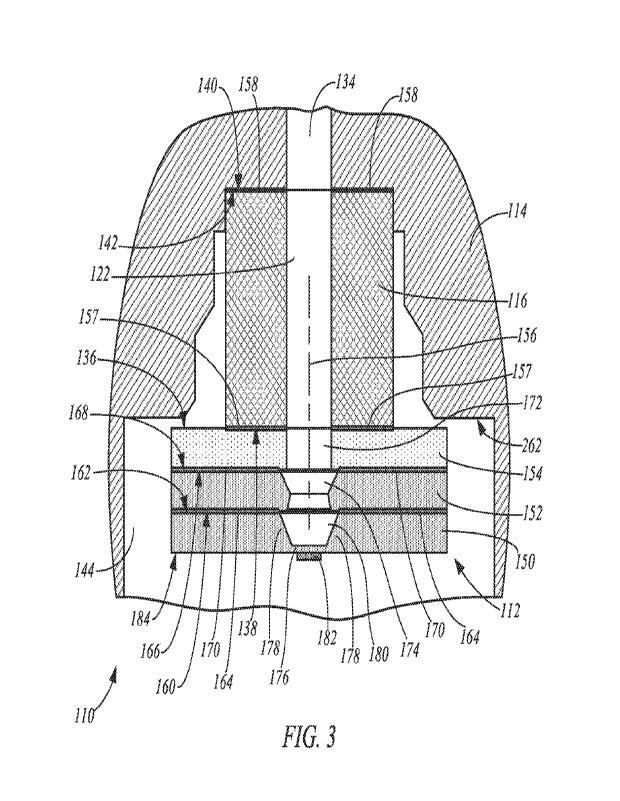
[0030] FIG. 3 is a simplified cross-sectional view of a portion of a pressure
sensor assembly
110, such as a gauge pressure assembly, in accordance with embodiments of the
present
disclosure. The pressure sensor assembly 110 includes the pressure sensor 112
formed in
accordance with embodiments of the present disclosure, which is attached to
the electrically
conductive header 114 (e.g., stainless steel) through the pedestal 116. A top
surface 136 of the
pressure sensor 112 attaches to a bottom surface 138 of the pedestal 116, and
a top surface 140
of the pedestal 116 attaches to a surface 142 of the header 114, such as
within the cavity 144 of
the header 114.
[0031] In order to protect and ensure proper operation of the pressure sensor
112, it is necessary
to electrically isolate the pressure sensor 112 from the header 114, the
housing 104 and the
process coupling 108, which may be electrically conductive. Conventional
techniques for
providing such electrical isolation of the pressure sensor 112 generally
require the use of an
electrically insulative pedestal 116 that blocks electrical charges and
currents from the header
114 from reaching the pressure sensor 112. For example, the pedestal 116 may
include at least
a portion formed of ceramic or another electrically insulative material that
electrically isolates
CA 03182839 2022- 12- 14
WO 2021/257137 PCT/US2021/021519
7
the pressure sensor 112 from the header 114. However, such a configuration can
lead to high
stresses in the junction of the electrically insulative pedestal 116 and the
pressure sensor 112
due to substantially non-matching thermal expansion coefficients of the
materials.
[0032] Some embodiments of the present disclosure relate to an improved
pressure sensor
design having integrated electrical isolation features. Some of the electrical
isolation features
may be implemented at the wafer stack assembly stage, resulting in significant
reductions in
cost and complexity, while providing improved quality. Additional advantages
of some
embodiments include pressure sensor geometries that provide enhanced stress
isolation, and
other advantages.
[0033] One embodiment of the pressure sensor 112 includes an electrically
conductive sensing
layer 150, an electrically conductive backing layer 152, and an electrically
insulative layer 154,
as shown in FIG. 3. In some embodiments, the conductive sensing layer 150 and
the conductive
backing layer 152 each comprise crystalline silicon and may be formed in
separate wafers. The
electrically insulative layer 154 electrically isolates the sensing layer 150
from the pedestal 116
and the header 114. The electrically insulative layer 154 may be formed of or
include glass,
ceramic, borosilicate glass, silicon nitride, silicon dioxide or aluminum
nitride ceramic, for
example, and may also be formed in a wafer. In some embodiments, each of the
layers 150, 152
and 154 has a thickness that is measured along an axis 156 of the pressure
sensor that may be
less than 20 mils, such as 12.5 mils.
[0034] Due to the electrical isolation built into the pressure sensor 112, it
is not necessary for
the pedestal 116 to provide the electrical isolation function in accordance
with conventional
pedestals 116. Some embodiments take advantage of this to reduce stresses at
the junction
between the pedestal 116 and the header 114, and the junction between the
pedestal 116 and
the pressure sensor 112. In some embodiments, the pedestal 116 is formed of an
electrically
conductive material, such as Kovar or another suitable conductive material,
and includes a
substantially planar surface 138 that is bonded to a substantially planar
surface 136 of the
electrically insulative layer 154, as shown in FIG. 3. Preferably, the
electrically insulative layer
154 is formed of a material, such as those mentioned above, having a similar
coefficient of
thermal expansion as the material forming the pedestal 116, to further reduce
the likelihood of
significant stresses developing at their junction. In some embodiments, a bond
157 between the
surface 136 of the electrically insulative layer 154 and the surface 138 of
the pedestal 116 may
CA 03182839 2022- 12- 14
WO 2021/257137
PCT/US2021/021519
8
be formed by a solder joint or another suitable bond. A bond 158 between the
pedestal 116 and
the header 114 may comprise a braze joint, or another suitable bond.
[0035] The electrically conductive backing layer 152 has a bottom surface 160
that is bonded
to a top surface 162 of the sensing layer 150 by a bond 164, and the
electrically insulative layer
154 has a bottom surface 166 that is bonded to a top surface 168 of the
backing layer 152 by a
bond 170. The bonds 164 and 170 may include glass frit bonds, which may
include an
electrically insulative material on the surfaces to be joined (e.g., thermally
grown silicon
dioxide), and may increase the electrical isolation of the sensing layer 150
from the pedestal
116 and the header 114. Alternatively, the bonds 164 and 170 may comprise a
thermocompression bond, a fusion bond, an anodic bond, or another suitable
bond.
[0036] In some embodiments, the bond 170 between the backing layer 152 and the
electrically
insulative layer 154 seals (e.g., hermetically seals) the junction of a
pathway 172 through the
electrically insulative layer 154 and a pathway 174 through the backing layer
152. Additionally,
the bond 157 between the electrically insulative layer 154 and the pedestal
116 (e.g., solder
joint) also seals (e.g., hermetically seals) the junction of the fluid pathway
134 through the
pedestal 116, and the fluid pathway 172 through the electrically insulative
layer 154.
[0037] The sensing layer 150 is configured to sense the pressure P using a
sensor diaphragm
176 that extends between perimeter support regions 178. The sensor diaphragm
176 has a
reduced thickness measured along the axis 156 of the sensor 112 relative to
the perimeter
support regions 178. A cavity 180 is formed in the sensing layer 150 between
the perimeter
support regions 178 and the sensor diaphragm 176. The bond 164 between the
backing layer
152 and the sensing layer 150 seals (e.g., hermetically seals) the pathway 174
to a cavity 180.
Thus, the cavity 180 may be exposed to ambient pressure through the pathway
134, while the
cavity 144 on the opposing side of the sensor diaphragm 176 is exposed to the
process pressure
P communicated by the fill fluid through the fluid pathway 122 (FIG. 1).
[0038] The sensor diaphragm 176 flexes or deflects in response to the pressure
difference
between the pressure P within the cavity 144 and the pressure within the
cavity 180. A known
relationship between the deflection of the diaphragm 176 and the pressure P is
used to measure
the pressure P.
[0039] In one embodiment, a sensor element 182 is used to detect the
deflection of the sensor
diaphragm 176 and thereby detect the pressure P. The sensor element 182 may be
mounted
CA 03182839 2022- 12- 14
WO 2021/257137 PCT/US2021/021519
9
within or on the sensor diaphragm 176, such as on a surface 184 of the sensing
layer 150, as
indicated in FIG. 3, and has an electrical parameter that changes based on the
deflection of the
sensor diaphragm 176. The measurement circuitry 124 may detect or receive a
measurement of
the electrical parameter of the sensor element 182 through the electrical
connection 126.
[0040] In some embodiments, the sensor element 182 may comprise one or more
strain gauges.
As the sensor diaphragm 176 deflects in response to the process pressure P
within the cavity
180, an electrical parameter of the strain gauge (e.g., in resistance) changes
and is representative
of the process pressure P.
[0041] FIGS. 4A-D are simplified side cross-sectional views illustrating an
example of a
method of producing the pressure sensor 112 and the pressure sensor assembly
110, in
accordance with embodiments of the present disclosure. In some embodiments,
the sensing
layer 150, the backing layer 152 and the electrically insulative layer 154 may
each be formed
in their respective wafers, as indicated in phantom lines. Additionally,
multiple formations of
the sensing layer 150, the backing layer 152 and the electrically insulative
layer 154 may be
formed in each wafer to allow for mass production of the sensors. The features
of the layers
150, 152 and 154 may be formed in the wafers using conventional etching, or
other suitable
techniques.
[0042] As indicated in FIG. 4A, the backing layer 152 and the electrically
insulative layer 154
may be provided with the pathway 174 of the backing layer 152 aligned with the
pathway 172
of the electrically insulative layer 154. The surface 168 of the backing layer
152 is then bonded
to the surface 166 of the electrically insulative layer 154 by the bond 170,
as indicated in FIG.
4B. As mentioned above, the bond 170 seals the junction between the pathway
174 of the
backing layer 152 and the pathway 172 of the electrically insulative layer
154.
[0043] The sensing layer 150 may be positioned such that the cavity 180 is
aligned with the
pathway 174 of the backing layer 152, as indicated in FIG. 4C. The surface 162
of the sensing
layer 150 is then bonded to the surface 160 of the backing layer 152 using the
bond 164 to form
the pressure sensor 112 shown in FIG. 4D. In some embodiments, the bond 164
seals the
junction between the pathway 174 of the backing layer 152 and the cavity 180.
[0044] Embodiments of the method are not limited to the particular order
described above. For
example, the sensing layer 150 could be bonded to the backing layer 152 prior
to bonding the
backing layer 152 to the electrically insulative layer 154. Other adjustments
may also be made.
CA 03182839 2022- 12- 14
WO 2021/257137 PCT/US2021/021519
[0045] In some embodiments of the method, a metal layer 186 is formed on the
surface 136 of
the electrically insulative layer 154, as shown in FIG. 4D. The metal layer
186 may comprise
solder for attaching the surface 136 of the electrically insulative layer 154
to the surface 138 of
the pedestal 116, as shown in FIG. 3. The pressure sensor assembly 110 (FIG.
3) may then be
completed by connecting the pedestal 116 to the header 114, such as by forming
the bond (e.g.,
braze joint) 158 between the surface 140 of the pedestal 116 and the surface
142 of the header
114.
[0046] When, the pressure sensor 112 shown in FIG. 4D is one of a plurality of
pressure sensors
formed in the stack of the wafers, each of the pressure sensors 112 may be cut
from the stack
of the wafers using a suitable die cutting process that cuts along lines 188
to separate the
individual pressure sensors 112 from the stack of wafers.
[0047] FIG. 5 is a simplified cross-sectional view of another example of a
pressure sensor 112
and a pressure sensor assembly 110, in accordance with embodiments of the
present disclosure.
The pressure sensor 112 includes an electrically conductive sensing layer 150,
which may
include one or more features described above, and a backing layer assembly 190
comprising
one or more electrically conductive backing layers 152, such as backing layers
152A and 152B.
As discussed above, these layers may comprise crystalline silicon and may be
formed in
separate wafers. Additionally, multiple pressure sensors 112 may be formed
simultaneously
through the stacking and bonding of the wafers, as discussed above.
[0048] A pathway 192 extends through the backing layer assembly 190 and
connects with the
cavity 180. In the example shown in FIG. 5, the pathway 192 through the
backing layer
assembly includes a pathway 192A through the electrically conductive backing
layer 152A and
a pathway 192B through the electrically conductive backing layer 152B.
Junctions along the
pathway 192 may be sealed by the bonds 194 and 196 connecting the layers
together.
[0049] A surface 198 of the backing layer assembly 190, such as the top
surface of the
electrically conductive backing layer 152A, may be configured to connect to
the pedestal 116
using any suitable technique. In one embodiment, a metal layer 186, such as a
layer of solder,
is formed on the surface 198 of the backing layer assembly 190 and is used to
attach the pressure
sensor 112 to the pedestal 116, as indicated in FIG. 5. The pedestal 116 may
then be attached
to the header 114 (FIG. 3), as discussed above with regard to the pressure
sensor 112.
CA 03182839 2022- 12- 14
WO 2021/257137 PCT/US2021/021519
11
[0050] In some embodiments, the pressure sensor 112 does not rely upon an
electrically
insulative layer, such as the layer 154 of the pressure sensor 112 (FIG. 3),
for electrical isolation
of the sensing layer 150 and/or sensor element 182. Rather, electrical
isolation of the sensing
layer 150 or the sensor element 182 is provided by the bond 194 formed between
the sensing
layer 150 and the backing layer assembly 190, and/or a bond between layers of
the backing
layer assembly 190, such as the bond 196 between the backing layer 152A and
the backing
layer 152B.
[0051] FIG. 6 is a magnified view of the portion 200 of FIG. 5, and
illustrates an example of
an electrically insulative bond 194, in accordance with embodiments of the
present disclosure.
In one embodiment, the electrically insulative bond 194 comprises layers or
coatings 202 of an
electrically insulative material, such as thermally grown silicon dioxide, on
the surface 162 of
the sensing layer 150 and the surface 206 of the backing layer 152B, and a
glass layer 208
between the coatings 202 for forming the bond (e.g., glass fit bond) with the
coatings 202 and
the surfaces 162 and 206. A glass frit bond 194 may be used to fuse the glass
layer 208 to the
coatings 202 and seal the junction of the pathway 192B and the cavity 180. A
similar technique
may be used to form the bond 196 between the backing layers 152A and 152B.
[0052] In some embodiments, the coatings 202 may each have a thickness 210
measured along
the axis 156 of the pressure sensor 112 of approximately 0.1 mils, and the
glass layer 208 may
have a thickness 212 of approximately 0.6 mils. Thus, the thickness of the
electrically insulative
bond 194 or 196 may be approximately 0.8 mils.
[0053] While the one or more electrically insulative bonds may block an
electrical charge from
being conducted from the pedestal 116 to the sensing layer 150 or sensor
element 182, the
thickness of each electrically insulative bond 194. 196 may not provide a
sufficient gap between
the uninsulated and exposed side surfaces 214 of the pressure sensor 112, such
as after the
sensor 112 is die cut from a wafer stack, to prevent electrical arcing (high-
potential failure)
around the bonds, as indicated by the arrows 216 in FIG. 5. For typical
voltages that may be
applied to the pressure sensor 112 from the header 114 and the pedestal 116, a
gap of
approximately 5 mils between the conductive surfaces 214 is necessary to
prevent such
electrical arcing. Thus, the electrically insulating bonds 194 and 196 may not
provide sufficient
protection for the sensing layer 150 or the sensor element 182 from high-
potential failures.
CA 03182839 2022- 12- 14
WO 2021/257137 PCT/US2021/021519
12
[0054] FIGS. 7-11 are simplified cross-sectional views of pressure sensor
assemblies 110 and
pressure sensors 112 that include features for preventing electrical arcing
between the
uninsulated sides 214 of the pressure sensor 112, in accordance with
embodiments of the
present disclosure. In some embodiments, a groove or notch 220 is formed in
the exposed and
uninsulated side surface or surfaces 214 of the sensing layer 150 and/or the
backing layer
assembly 190. The notch 220 extends around the perimeter of the pressure
sensor 112 and
defines a gap 222 extending along the axis 156 that is sufficient to prevent
electrical arcing
between the electrically conductive side surfaces 214. For example, the gap
222 may extend a
distance along the axis of greater than 5 mils, such as 8 mils or 10 mils, as
shown in FIGS. 8-
12.
[0055] The notch 220 may be formed in the sensing layer 150 and/or one or more
of the backing
layers 152 of the backing layer assembly 190 using any suitable technique,
such as with a
potassium-hydroxide (KOH) wet etching process. For example, the notch 220 may
be formed
in the adjoining backing layers 152A and 152B of the backing layer assembly,
as shown in FIG.
7. This may be a preferred location for the notch when the backing layers 152
are formed of
relatively thin wafers, such as wafers having a thickness of less than 20
mils, such as 12.5 mils,
for example.
[0056] FIGS. 8-10 illustrate examples of the pressure sensor 112 in which the
notch 220 is
formed in a single backing layer 152A or 152B of the backing layer assembly
190. In some
embodiments, the backing layer 150 containing the notch 220 has a thickness of
greater than
12.5 mils, such as 20 mils or 35 mils. for example. In FIGS. 8 and 9, the
notch is formed in the
lower backing layer 152A that attaches to the pedestal 116, and in FIG. 10,
the notch 220 is
formed in the upper backing layer 152B that attaches to the sensing layer 150.
[0057] In some embodiments, the insulating bond 196 between the backing layers
152A and
152B may extend across the larger of the adjoining surfaces, such as the
bottom surface 224 of
the backing layer 152B, as shown in FIG. S. Alternatively, the bond 196 may
extend across the
shorter of the adjoining surfaces and does not extend over the larger of the
adjoining surfaces.
For example, the bond 196 may extend over the surface 226 of the backing layer
152A, as
shown in FIG. 9, or the surface 224 of the backing layer 152B, as shown in
FIG. 10.
[0058] FIG. 11 is a simplified cross-sectional view of a pressure sensor
assembly 110 that
includes a pressure sensor 112 having a notch 220 that extends between the
sensing layer 150
CA 03182839 2022- 12- 14
WO 2021/257137 PCT/US2021/021519
13
and the backing layer assembly 190. Here, the backing layer assembly 190
includes a single
conductive backing layer 152. An electrically insulative bond 194 joins the
bottom surface 162
of the sensing layer 150 to the surface 206 of the backing layer 152. The
thickness of the sensing
layer 150 and the thickness of the backing layer 152 measured along the axis
156 may be
approximately 10-15 mils, such as 12.5 mils, for example.
[0059] Additional embodiments of the present disclosure relate to pedestal
structures in one or
more layers of the pressure sensor 112, such as an electrically insulative
layer (e.g., layer 154
of the pressure sensor of FIG. 3) or an electrically conductive backing layer
(e.g., layer 152A
or 152B). The pedestal structures provide stress isolation to the sensing
layer 150 by reducing
a contact area between adjoining layers of the pressure sensor 112. This
reduces the likelihood
of harmful stresses reaching the sensing layer 150 that may adversely affect
its operation. Each
of the pedestal structures may be formed through wet etching or another
suitable technique.
[0060] In some embodiments, the pedestal structures within a layer include a
wall that
surrounds the axis 156 of the pressure sensor 112 and an opening of the
pathway extending
through the layer, and defines a cavity of the pathway. The wall reduces the
contact area
between adjoining layers of the pressure sensor 112 and assists in providing
stress isolation to
the sensing layer 150.
[0061] One example of this wall feature is shown in the pressure sensors 112
of FIGS. 8 and 9,
in which the backing layer 152A includes a wall 230 that extends vertically
along the axis 156
from the top surface 198 to the bottom surface 226 of the backing layer 152A.
The wall 230
surrounds the axis 156, and includes an interior surface 232 that defines a
boundary of a cavity
234 of the pathway 192A through the backing layer 152A. An exterior surface
236 of the wall
230 may define an interior surface of the notch 220.
[0062] In some embodiments, a surface 238 extends from the wall 230 to an
opening 240 of
the pathway 192A. A contact area 242 is formed on the wall 230 and engages or
is joined to the
adjoining layer of the pressure sensor 112, which, in this example, is the
backing layer 152B,
through the corresponding bond 196. The small contact area 242 between the
backing layer
152A and the backing layer 152B through the bond 196 isolates stresses that
may develop in
the backing layer 152A due to its attachment to the pedestal 116, and reduces
the transfer of
those stresses to the sensing layer 150.
CA 03182839 2022- 12- 14
WO 2021/257137 PCT/US2021/021519
14
[0063] Additional examples of the wall feature are shown in FIG. 10, in which
the wall 230 is
formed in the backing layer 152B and the small contact surface 242 is formed
at the surface
224.
[0064] FIGS. 12 and 13 respectively are a cross-sectional view of a pressure
sensor assembly
110 and a bottom plan view of a backing layer 152A of the assembly 110 of FIG.
12, in
accordance with embodiments of the present disclosure. Here, the notch 220
penetrates the side
surface 214 of the backing layer 152A a farther distance toward the axis 156
than in the
examples shown in FIG. 7. This results in the formation of a wall 230 that
operates similarly to
the walls discussed above. For example, the wall 230 extends from the surface
198 to the surface
196 of the backing layer 152A, and the surface 196 has a reduced contact area
242 with the
surface 224 of the adjoining backing layer 152B through the bond 196, which
may be an
electrically insulative bond, relative to the example shown in FIG. 8.
[0065] FIGS. 14 and 15 respectively are a cross-sectional view of a pressure
sensor assembly
110 and a bottom plan view of a backing layer 152A of the assembly 110 of FIG.
14, in
accordance with embodiments of the present disclosure. In this example, the
backing layer
152A includes multiple walls 230, such as walls 230A and 230B. Each of the
walls 230
surrounds the axis 156 and the fluid cavity 192A through the backing layer
152A, and the wall
230A surrounds the wall 230B. The walls 230A and 230B reduce the contact area
with the
adjoining backing layer 152B relative to the example shown in FIG. 7, and
isolate the sensing
layer 150 from stresses in the backing layer 152A. The wall 230A has a contact
area 242A of
the surface 226 that contacts or is attached to the surface 224 of the backing
layer 152B through
the bond 196, and the wall 230B has a contact area 242B of the top surface 226
that contacts or
is attached to the surface 224 of the backing layer 152B through the bond 196.
As discussed
above, the bonds 196 may be electrically insulative bonds. An exterior surface
236A of the wall
230A may form an interior surface of a notch 220, and the interior surface
232A of the wall
230A may define a boundary of an interior cavity 244. The interior cavity 244
may be sealed
from both the pathway 192 and the sensor exterior, which may reduce or
minimize the stress
induced on the diaphragm 176 from the sensor mounting by reducing the rigidity
of the backing
layer 152A. An exterior surface 236B of the wall 230B may define a boundary of
the cavity
244, and an interior surface 232B of the wall 230B may define a boundary of
the cavity 234 of
the pathway 192A through the backing layer 152A.
CA 03182839 2022- 12- 14
WO 2021/257137 PCT/US2021/021519
[0066] FIG. 16 is a simplified cross-sectional view of a pressure sensor
assembly 110, in
accordance with embodiments of the present disclosure. In the pressure sensor
assembly 110
example provided in FIG. 16, the layer 256 of the pressure sensor 112 allows
for a shorter
pedestal 116 relative to the pressure sensor assembly 110 of FIG. 3, for
example. Here, the layer
256 of the pressure sensor 112 may take the form of an electrically insulative
layer, such as
layer 154 of the pressure sensor 112 of FIG. 3, or an electrically conductive
backing layer, such
as the layer 152 of FIG. 5.
[0067] As shown in FIG. 16, the layer 256 is shaped relative to its wafer form
(dashed lines) to
maintain a gap 258 between the layer 256 and the header 114, while allowing
the surface 260
of the layer 256 to be positioned along the axis 156 above a shoulder 262 of
the header 114,
rather than below the shoulder 262 of the header 114, as shown in FIG. 3. This
allows the height
264 of the pressure sensor 112 measured along the axis 156 from the shoulder
262 of the header
114 to be reduced relative to other configurations, such as that shown in FIG.
3. Additionally,
the pedestal 116 may be formed shorter, allowing the surface 138 of the
pedestal to be
positioned above the shoulder 262 of the header 114. As a result, the pressure
sensor assembly
110 may be formed more compactly than other pressure sensor assembly designs,
such as that
shown in FIG. 3. Additionally, the shorter fluid pathway 122 from the base 142
of the header
114 (FIG. 3) to the cavity 180 allows for a reduction in the fill fluid volume
that is used by the
pressure sensor assembly 110.
[0068] As discussed above, in some embodiments a metal layer 186 (FIGS. 4D and
5), such as
solder, is applied to the top of the pressure sensor 112 to facilitate
attachment of the pressure
sensor 112 to the pedestal 116. Some embodiments of the present disclosure
include features
that reduce the potential for contamination of the pathway through the
pressure sensor 112 and
the cavity 180 with the applied metal when the metal layer 186 is applied.
[0069] In one example, one or more restrictions 270 are created in the pathway
of the pressure
sensor 112, such as shown in FIGS. 4D and 5. In one embodiment, each
restriction 270 is
formed by a tapered section of the pathway, such as that provided in the layer
152 of the pressure
sensor 112 shown in FIG. 4D, and in the layers 152A and 152B of the pressure
sensor 112
shown in FIG. 5. Each restriction 270 provides a partial block to potential
contamination of the
pathway through the pressure sensor 112 and the cavity 180 during application
of the metal
CA 03182839 2022- 12- 14
WO 2021/257137 PCT/US2021/021519
16
layer 186 to the surface 198 of the backing layer 152A. Such restrictions 270
may also be
formed in the electrically insulative layer 154 of the pressure sensor 112 of
FIG. 4D.
Although the embodiments of the present disclosure have been described with
reference to
preferred embodiments, workers skilled in the art will recognize that changes
may be made in
form and detail without departing from the spirit and scope of the present
disclosure.
Embodiments of the present disclosure include combinations of one or more of
the
embodiments described herein. For example, the sensor element may comprise a
capacitive
electrode having a capacitance, which is measured between the capacitive
electrode and a
reference electrode, that indicates the process pressure P.
CA 03182839 2022- 12- 14