Note: Descriptions are shown in the official language in which they were submitted.
COMPACT AND EASILY PRODUCIBLE MEMS PACKAGE WITH
ENHANCED PROTECTIVE PROPERTIES
DESCRIPTION
Preferably, the invention relates to a MEMS package having at least one layer
for protecting a
MEMS element, wherein the MEMS element has at least one MEMS interaction
region on a
substrate and a surface conformal coating of the MEMS element is applied with
a dielectric layer.
Particularly preferably, the invention relates to a MEMS transducer package in
which a MEMS
element, for example with a MEMS membrane and a processor, preferably an
integrated circuit,
are present on a substrate. For protection, a surface conformal coating of a
dielectric is preferably
first applied to the MEMS element, for example by spray coating, mist coating,
and/or vapor
coating. Then, preferably, an electrically conductive layer is applied.
Depending on the
configuration, the layers may be removed in regions above a MEMS interaction
region of the
MEMS element, for example for a sound port of a MEMS membrane.
Background and prior art
Today, microsystems technology is used in many fields of application for the
production of
compact, mechanical-electronic devices. The microsystems
(microelectromechanical systems,
MEMS for short) that can be produced in this way are very compact (micrometer
range) with
excellent functionality and ever lower production costs.
Applications of MEMS technology include MEMS-based optical emitters or
receivers, filters,
electrochemical sensors, gas sensors, or even MEMS acoustic transducers.
MEMS transducers are preferably MEMS sound transducers and can be designed,
for example,
as MEMS microphones or as MEMS loudspeakers. Both functionalities can also be
fulfilled by one
MEMS transducer. Such MEMS transducers are used, for example, in modern
smartphones.
MEMS transducers preferably comprise a MEMS device (e.g. MEMS chip) with a
vibratable
membrane, the vibrations of which are generated and/or read out, for example,
by piezoelectric or
piezoresistive components on or at the membrane. Likewise, capacitive methods
for generating
and/or measuring vibrations of the membrane are known.
The MEMS transducers are often arranged on a substrate together with an
integrated circuit (IC)
for controlling and/or evaluating the oscillations and are in contact with
these via electrical
connections, which are made, for example, by wire bonds and/or are applied in
the substrate, e.g.
1
CA 03182872 2022- 12- 14
by conductor tracks. The substrate functions in particular as a carrier and
can be designed, for
example, as a printed circuit board (PCB) or as a ceramic. In addition to the
carrier function, it can
preferably also implement electrical functions, e.g. provide electrical
connections for the individual
components.
An IC is preferably an electronic component by which a control unit or a
regulation unit is realized.
In particular, it is an electronic chip. This can, for example, have an
application-specific integrated
circuit (ASIC), which is particularly suitable for mass production. However,
it can also be a
programmable logic device (PLD), e.g. a field programmable gate array (FPGA),
especially for
individual applications.
MEMS elements, such as a MEMS transducer, are mostly sensitive to external
influences and are
therefore protected by so-called packaging.
In this respect, the packaging of MEMS elements fulfills several tasks. These
include protecting
the component from dust, moisture and liquids, as well as from ESD
(electrostatic discharge). At
the same time, however, the functional properties of the MEMS element, for
example the acoustic
properties of an acoustic MEMS transducer, should be preserved.
The package preferably fulfills a housing function for the MEMS element. On a
bottom side of the
MEMS element, a substrate itself can fulfill this function. In addition,
protection is required above
the substrate for the components arranged on it.
The MEMS device or the MEMS device can be arranged on the substrate
conventionally or in a
so-called flip-chip assembly, whereby the chip is mounted with the active
contacting side facing
downwards towards the substrate and without further connecting wires. For this
purpose, the
substrate itself preferably has contact bumps. This advantageously leads to
small dimensions of
the housing and short lengths of the electrical conductors.
The MEMS device and/or MEMS membrane may be present on the substrate in a MEMS
acoustic
transducer in a variety of ways.
The volume in which sound waves are to be measured and/or generated as seen
from the MEMS
membrane is preferably referred to as the front volume. The other side is
preferably referred to as
the back volume. This is preferably closed and has no direct connection to the
front volume except
possibly via an opening in the membrane. Depending on the arrangement, the
back volume can
be located, for example, between the membrane and the substrate. In this case,
the front volume
is located above the MEMS device and substrate. A housing component located
here (e.g. a
cover), which closes the package at the top, preferably has a sound port in
this region.
2
CA 03182872 2022- 12- 14
However, the back volume can also be located between the membrane and the
housing
component arranged above the MEMS device and substrate. This is then
preferably completely
closed. The front volume is then preferably located between the membrane and a
sound port in
the substrate. Dimensions and geometry of these volumes as well as their size
ratio influence the
acoustic properties of the MEMS transducer. The MEMS membrane can preferably
be present in
both described constellations within the height of the MEMS device, either
arranged at an upper
end or at a lower end, towards the substrate.
In the case of a MEMS transducer, the electrical components of the MEMS device
itself, e.g.
electrodes of a capacitive MEMS transducer are preferably present in the back
volume or
arranged towards the back volume (e.g. on the side of the membrane oriented
towards the back
volume), for example to enable the measurement of some liquids by the membrane
without short-
circuiting or contaminating these components. Preferably, this allows the
fluid to be in direct
contact with the membrane. General protection against short circuits caused by
moisture is also
achieved in this way. However, a prerequisite for this is that the package
prevents moisture/liquid
from entering other areas of the MEMS transducer via the sound port. A sound
port in the
package should therefore be an opening only to the membrane, not to other
areas of the MEMS
transducer.
Prior art packages (see e.g. Dehe et al. 2013) for MEMS transducers have a
metal cover. These
covers enclose a volume that is significantly larger than theoretically needed
for the underlying
components of the MEMS transducer. The main reason for this is to maintain a
distance between
the cover and the components, some of which are electrically conductive (e.g.
wire bonds,
electrodes of capacitive MEMS transducers, etc.), to avoid short circuits. At
the same time, metal
is desirable as a starting material for these covers because it is
mechanically stable and
hermetically sealed, especially against water and air. Hermetically sealed
refers in particular to
impermeability under the transducer's usual operating conditions, i.e.
preferably also at pressures
that are considerably higher than atmospheric pressure. In addition, sensitive
components can be
electromagnetically shielded. In this way, negative influences and
electrostatic discharges (ESD)
can be avoided. However, these covers counteract the compact design of modern
MEMS
transducers.
Metal covers can be provided with an opening for sound. Even then, however,
direct contacting of
the MEMS membrane with a material to be measured (solid, gas, liquid) is
difficult because the
opening is located at some distance above the membrane (see above) and this
distance would
have to be overcome. In addition, because the cover and opening are not flush
with the
transducer components, liquid can get into the space between the cover and the
MEMS devices,
3
CA 03182872 2022- 12- 14
which can cause short circuits between their electrically conductive regions
and promote the
ingress of dirt and other harmful substances.
A sound port through the substrate (see also Dehe et al.) has in particular
the disadvantage that
due to the dimensions of the aperture and the length of the aperture, which is
predetermined at
least by the thickness of the substrate, a low-pass filter for sound
frequencies is created, which in
particular opposes the usability of an ultrasonic transducer.
So-called flip-chip packages (Feiertag et al., 2010) can reduce the height of
the covers because
they no longer have to be designed for wire bonds. However, the
miniaturization effect is also
small here.
The use of metallized polymer films as an outer packaging layer is also known
from Feiertag et al.
For this purpose, polymer films are laminated onto the upper side of the MEMS
transducers and
then provided with a metal layer. However, the process is costly. In addition,
the film must be
thermally deformed for this purpose and/or heated by laser ablation during
post-
processing/structuring, which introduces temperature into the MEMS transducer.
Heating makes thermoplastics easier to form, which is used in comparable blow
molding or
thermoforming of polymers. However, in all these processes, additional stress
is exerted on the
component. This can introduce stresses into the component or cause other
damage as well as
unwanted outgassing. It is also difficult to place the film flush and tightly
over the MEMS
transducer on all sides, so leakage from the package environment can occur and
the compact
design suffers.
US 6,956,283 B1 discloses a method for protecting components of a MEMS sensor
from external
influences in a "package first, release later" approach. A matrix array of
micromirrors is placed on
a silicon chip, which in turn is placed on a substrate. In the proposed
method, a protective layer is
applied to the substantial components of the sensor. Various methods can be
used for coating,
such as spraying or vacuum coating. After deposition, the protective layer is
removed over an
active region. Finally, a cover is applied as a protective housing.
US 2019/0148566 Al relates to a production method of a semiconductor sensor
element, wherein
it can be a pressure sensor, a gas sensor, or a capacitive sensor. The
semiconductor sensor
element comprises a substrate, on which a semiconductor element is located,
which is connected
to the substrate via bonding wires. A dielectric layer is deposited on the
semiconductor sensor
element via an evaporation process. Laser beams can be used to partially
remove the dielectric
layer. A cover is used to protect the semiconductor element from external
forces.
4
CA 03182872 2022- 12- 14
US 2019/0311961 Al discloses a semiconductor sensor comprising a substrate
with a chip
thereon. A film layer is deposited on the components of the semiconductor
sensor to protect it, for
example, from external gases, liquids, etc. The film layer is preferably
applied via vapor deposition
and over all components of the sensor that are located within the package. The
housing includes
an opening and is used to protect and support the components of the
semiconductor sensor.
A MEMS package that can function without a rigid lid or package is not known
in the prior art.
In light of the disadvantages of the prior art, there is thus a need for
alternative or improved
packages as well as production methods for packages for MEMS elements, in
particular MEMS
transducers.
Objective of the invention
The objective of the invention is to provide a MEMS package as well as a
method for production
such a MEMS package, which do not have the disadvantages of the prior art. In
particular, one
objective of the invention was to provide a MEMS package which is very
compact, at the same
time offers the MEMS element, for example a MEMS transducer, a high level of
protection against
dust, moisture, liquids and ESD and ensures the desired functional properties,
for example
acoustic properties in the case of a MEMS transducer. The package is also said
to be particularly
easy and cost-effective to produce and suitable for mass production due to
fewer and simple
steps.
Summary of the invention
The objective is solved by the features of the independent claims. Preferred
embodiments of the
invention are described in the dependent claims.
The invention preferably relates to a production method for a MEMS package
having at least one
layer for protecting a MEMS element, comprising the following steps:
- Providing a MEMS element comprising at least one MEMS
interaction region on a
substrate
- Surface conformal coating of the MEMS element with a
dielectric layer.
Preferably, the MEMS interaction region is an essential functional component
of the MEMS
element, which preferably interacts with a medium in a desired manner.
A surface conformal coating is, in particular, a coating that is substantially
in direct and form-
retaining close contact with the underlying structures.
5
CA 03182872 2022- 12- 14
Substantially direct and form-retaining preferably means that the majority of
the coating is in direct
contact, but includes volumes not filled by components in some regions, for
example in corner
regions or below a wire bond.
The surface conformal coating is preferably completely surface conformal. This
means in
particular that the coating is almost perfectly close-fitting or surface
conformal and even the
smallest structures can be coated in a close-fitting manner. The smallest
structures are preferably
structures with dimensions of the order of maximum 10 nanometers (nm), maximum
100 nm,
maximum 1 micrometer (pm), maximum 10 pm or maximum 100 pm.
The dielectric layer preferably comprises at least one polymer. These are
inexpensive and easy to
process. It may also be preferable to apply an oxide or nitride layer as the
dielectric layer. For
surface conformal coating, physical or chemical vapor deposition (PVD and CVD)
are particularly
suitable for this purpose.
In a preferred embodiment, the polymer is a photostructurable polymer, e.g. by
appropriate
admixtures of photosensitive components. In particular, it is a photoresist.
Advantageously, the properties of the polymer can be adapted to the
functionality of a MEMS
element. In the case of a MEMS transducer as a MEMS element, for example, it
may be
preferable to adapt the relative permittivity Cr of the polymer to high-
frequency applications of the
MEMS transducer. For example, Cr can be chosen to attenuate high-frequency
electro-magnetic
fields.
Such a functional coating with a dielectric is not possible with prior art
processes and
advantageously provides an extremely compact protective layer that provides
electrical insulation
and mechanical protection of the MEMS element.
In a preferred embodiment, the MEMS element is selected from the group:
optical MEMS
transducer, acoustic MEMS transducer, MEMS sensor, in particular MEMS gas
sensor and/or
MEMS filter. It was recognized by the inventors that the proposed packaging
can provide reliable
protection for a number of different MEMS elements by means of a dielectric
coating, preferably
with a polymer.
On the one hand, a hermetic, space-optimized protective layer can be applied
extremely cost-
effectively by surface conformal coating, for example by a spray process with
a polymer. On the
other hand, the surface conformal coating, for example using photostructurable
polymers, allows a
high degree of flexibility with regard to a planned opening or recess of the
protective layer in an
interaction region of the MEMS element.
6
CA 03182872 2022- 12- 14
The MEMS interaction region preferably means a functional component of the
MEMS element that
interacts with an external medium in a desired manner. In the case of an
acoustic MEMS
transducer, for example, it is a MEMS membrane. In the case of an optical MEMS
transducer, for
example, it is an optical emitter.
In both cases, it is preferred that, on the one hand, no protective layer is
applied directly in the
interaction region of the MEMS element thereby reducing the interaction of the
MEMS element
with the environment (sound emission or reception, transmission or reception
of optical signals),
while the protection of the sensitive electronic components is ensured. The
method according to
the invention achieves this in a simple and highly efficient manner by means
of a surface-form
coating preferably by applying a polymer.
In a preferred embodiment, the MEMS element is an optical MEMS transducer,
wherein the
MEMS interaction region comprises an optical emitter and/or an optical
receiver.
An optical emitter may include, for example, a surface emitter or VCSEL
(vertical-cavity surface-
emitting laser) or an LED. An optical receiver is, for example, a photodiode
or an image sensor.
In a preferred embodiment, the optical emitter may be a modulable MEMS
emitter. For example,
modulation of the intensity of the optical emitter can be accomplished using
aperture structures
and MEMS actuators, such as an electrostatic actuator, a piezoelectric
actuator, an
electromagnetic actuator, and/or a thermal actuator.
In a preferred embodiment, the MEMS element is a MEMS acoustic transducer,
wherein the
MEMS interaction region comprises a MEMS membrane.
In a preferred embodiment, the MEMS transducer is a MEMS speaker, a MEMS
microphone,
and/or a MEMS ultrasonic transducer. Preferably, the MEMS membrane is
vibratable. A
membrane is preferably a thin, planar structure having a perimeter in, for
example, a substantially
circular and/or polygonal configuration. The membrane is preferably vibratable
at least regionally
along one of the perimeters.
Terms such as substantially, approximately, about, etc. preferably describe a
tolerance range of
less than 20%, preferably less than 10%, even more preferably less than
5% and in
particular less than 1%. Indications of substantially, approximately, about,
etc. always also
disclose and include the exact value mentioned.
A MEMS speaker or MEMS microphone preferably refers to a speaker or microphone
which is
based on MEMS technology and whose sound-generating or sound-receiving
structures at least
7
CA 03182872 2022- 12- 14
partially have dimensions in the micrometer range (1 pm to 1000 pm).
Preferably, the vibratable
membrane may have a dimension in the range of less than 1000 pm in width,
height and/or
thickness.
The term MEMS transducer refers to both a MEMS microphone and a MEMS speaker.
In general,
the MEMS transducer refers to a transducer for interaction with a volume flow
of a fluid, which is
based on MEMS technology and whose structures for interaction with the volume
flow or for
receiving or generating pressure waves of the fluid have dimensions in the
micrometer range (1
pm to 1000 pm). The fluid can be a gaseous fluid as well as a liquid fluid.
The structures of the
MEMS transducer, in particular the vibratable membrane, are designed to
generate or receive
pressure waves of the fluid.
For example, as in the case of a MEMS speaker or MEMS microphone, it may be
sound pressure
waves. However, the MEMS transducer may equally be suitable as an actuator or
sensor for other
pressure waves. Thus, the MEMS transducer is preferably a device that converts
pressure waves
(e.g., acoustic signals as sound pressure waves) into electrical signals or
vice versa (converting
electrical signals into pressure waves, such as acoustic signals).
MEMS transducers preferably comprise a MEMS device (e.g., MEMS chip) with a
vibratable
membrane whose vibrations are generated and/or read out, for example, by
piezoelectric or
piezoresistive components on or at the membrane.
In a preferred embodiment, the MEMS transducer is a piezoelectric MEMS
transducer.
Similarly, capacitive methods for generating and/or measuring vibrations of
the membrane are
known.
In a preferred embodiment, the MEMS transducer is a capacitive MEMS
transducer.
In preferred embodiments, MEMS transducers may also be MEMS ultrasonic
transducers suitable
for transmitting and/or receiving ultrasound.
In particular, these are capacitive micromechanical ultrasound transducers
(CMUT), piezoelectric
micromechanical ultrasound transducers (PMUT) or combined ultrasound
transducers
(piezoelectric composite ultrasound transducers, PC-MUT).
Ultrasound covers frequencies from 1 kilohertz (kHz), typically mainly from 16
kHz. Applications of
compact ultrasonic transducers include imaging methods, e.g. in medicine, but
also in the
measurement of other objects. Applications for ultrasonic density measurement,
for strength
measurement of concrete, gypsum and cement, for level measurement of liquid
and solid media of
8
CA 03182872 2022- 12- 14
different consistencies and surface properties or for an ultrasonic microscope
are also
conceivable. Here, it is often desirable that the membrane of the transducer
(i.e. of the MEMS
interaction region) is in direct contact with the object/liquid to be
measured.
With the method according to the invention for surface conformal coating of a
dielectric protective
layer, this can be advantageously achieved without impairing the protective
functions. Instead, in a
simple manner, the dielectric protective layer in the interaction region can
be removed in a
targeted manner, while the layer remains in close contact with the remaining
structures. In
particular with regard to acoustic MEMS transducers - such as MEMS microphones
or MEMS
speakers - influences on the acoustic behavior can be avoided in this way and
excellent detection
or sound results can be achieved.
In another preferred embodiment, the MEMS element is a MEMS gas sensor,
wherein the MEMS
interaction region comprises a MEMS membrane and/or a MEMS electrochemical
sensing region.
For example, it may be a photoacoustic spectroscope with a MEMS sensor.
In photoacoustic spectroscopy, intensity-modulated infrared radiation is
preferably used with
frequencies in the absorption spectrum of a molecule to be detected in a gas.
If this molecule is
present in the beam path, modulated absorption takes place, leading to heating
and cooling
processes whose time scales reflect the modulation frequency of the radiation.
The heating and
cooling processes lead to expansions and contractions of the gas, causing
sound waves at the
modulation frequency. These can be measured by sensors such as sound detectors
or flow
sensors.
Preferably, the power of the sound waves is directly proportional to the
concentration of the
absorbing gas. Thus, a photoacoustic spectroscope preferably comprises at
least one emitter, a
detector, and a cell. In a MEMS gas sensor, the detector is preferably
implemented as a MEMS
sensor.
For example, a MEMS sensor may include a capacitive or optically readable
piezoelectric,
piezoresistive, and/or magnetic beam and/or a capacitive, piezoelectric,
piezoresistive, and/or
optical microphone or membrane.
In terms of the invention, the MEMS sensor of a photoacoustic spectroscope can
preferably be
understood as its MEMS interaction region, since it is preferably in direct
contact with a medium.
9
CA 03182872 2022- 12- 14
In another preferred embodiment, the MEMS element is a MEMS filter, preferably
a MEMS
frequency filter, in particular a SAW or BAW filter, wherein the MEMS
interaction region comprises
a MEMS filter structure, in particular MEMS electrodes and/or a MEMS bulk
region.
A SAW filter is preferably an acoustic surface wave filter, (likewise AOW
filter), which is in
particular a bandpass filter for electrical signals.
These are preferably based on interference of signals of different transit
times and preferably use
the piezoelectric effect. Preferably, each piezoelectric single crystal
comprises a pair of comb-
shaped interlocking electrodes, which preferably form the interaction region.
BAW filters (bulk acoustic wave) are preferably similar electronic filters
with bandpass
characteristics. However, in contrast to the SAW filter, they preferably have
a substrate (bulk) in
which the propagation of the acoustic waves takes place. This substrate or
bulk area preferably
forms the MEMS interaction region.
In a preferred embodiment of the invention, the surface conformal coating is
performed by a
dielectric coating process, wherein the coating process is selected from the
group consisting of:
spray coating, mist coating, electroplating, and/or vapor coating.
Spray coating preferably refers to a two-dimensional application of the
dielectric layer, with the
dielectric preferably being pressurized before spraying (e.g. higher than the
prevailing ambient
pressure, e.g. in the case of atmospheric pressure preferably at more than 1
bar, more preferably
at more than 2 bar, in particular at 2 - 6 bar), so that fine
particles/aerosols of the dielectric and/or
a foam are formed. In this way, a particularly fine coating can be achieved
which covers all
sprayed areas, even if, for example, these have surfaces which are at an
unfavorable angle to the
spray direction. Even surfaces/regions that are angled relative to one another
can thus preferably
be covered directly. When using a film as in the known prior art, however, it
is extremely difficult to
cover such regions directly without creating uncovered volumes. This is due,
for example, to the
fact that the film is continuous and under tension.
Preferably, for the coating process, a liquid dielectric is atomized under
increased pressure
compared to the environment and applied over the surface.
Spray coating is preferably a spray paint.
The spray coating and/or surface conformal coating can also be a gas phase
deposition, in
particular if the dielectric layer comprises a polymer that can be deposited
from the gas and/or
CA 03182872 2022- 12- 14
liquid phase, e.g. tetraethyl orthosilicate (TEOS) and/or parylene. In this
way, a particularly close-
fitting or surface conformal coating can be achieved on the transducer
components.
A mist coating preferably comprises a coating by fine droplets of the
dielectric, which are finely
dispersed in an atmosphere (preferably a gas). A mist coating preferably
allows a fully surface
conformal coating to be achieved.
A vapor coating is preferably applied by a dielectric in vapor form, or in
gaseous form. A vapor
coating can, for example, comprise a PVD (physical vapor deposition) or a CVD
(chemical vapor
deposition). Vapor deposition advantageously enables a fully surface conformal
coating of a
dielectric.
In a preferred embodiment, the surface conformal coating is applied by
depositing a dielectric
layer using a physical vapor deposition (PVD) or chemical vapor deposition
(CVD) process.
In a preferred embodiment, the dielectric layer is an oxide or nitride layer,
which was preferably
deposited by means of a physical or a chemical vapor deposition (CVD).
An oxide or nitride layer may be, for example, a layer of a metal or semimetal
oxide or a metal or
semimetal nitride.
In a preferred embodiment, the dielectric layer is a layer comprising an
aluminum nitride, silicon
nitride, aluminum oxide, silicon dioxide, titanium dioxide, and/or tantalum
oxide. An electroplated
coating may also be included in the surface conformal coating. Electroplating
preferably refers to
the electrochemical deposition of coatings on substrates (in this case the
MEMS element).
In a preferred embodiment, the surface conformal coating is provided by a
coating wetting the
MEMS element at least in some regions.
Wetting preferably means completely wetting or substantially completely
wetting. Completely
wetting preferably means that the dielectric, which is preferably applied in
liquid form, spreads on
the surface in the form of a flat disc. In particular, there is no macroscopic
contact angle.
Preferably, it is a substantially nearly monomolecular film with a contact
angle of zero.
Preferably, the spreading parameter S describes the difference between the
surface tension of the
substrate (GS), the surface tension of the liquid (GL) and the interfacial
tension between substrate
and liquid (GSL). Preferably, this can be used to distinguish between complete
and partial wetting:
S = GS - GL -GSL
If S > 0, the dielectric completely wets the substrate. The case S < 0
characterizes partial wetting.
11
CA 03182872 2022- 12- 14
Preferred means completely wetting S> 0.
In a preferred embodiment, the dielectric, coating method, and/or a surface of
the MEMS element
are configured (at least regionally) for wetting coating.
How exactly the materials, the droplet size of the dielectric, the roughness
of a surface, etc. have
to be selected in order to obtain a desired wetting is known to the person
skilled in the art.
Approaches according to Harth et al., 2012, for example, can be followed to
calculate the relevant
variables.
In a preferred embodiment, the surface conformal coating is performed by de-
wetting the MEMS
element at least in regions, the regions preferably comprising the MEMS
interaction region.
Particularly preferably, the surface conformal coating is carried out by means
of a coating that
wets the MEMS element at least in certain regions, with a wetting coating
being applied in the
MEMS interaction region.
Dewetting preferably means that the dielectric contracts on the surface to
form a substantially
spherical drop and/or has a contact angle greater than 90 . With a slight
inclination of the surface,
the droplet preferably slides down without any liquid residue, in particular
the liquid (the dielectric)
beads off. Preferably, the dielectric has a contact angle of substantially 180
when applied to the
surface and the liquid droplet contacts the solid at substantially only one
point. This makes it
particularly easy to remove the dielectric from the MEMS interaction region
after coating.
In a preferred embodiment of the invention, the dielectric, coating method,
and/or regions of the
surface of the MEMS element, preferably the MEMS interaction region, are
configured for a
wetting coating.
Preferably, the same considerations play a role as in the case of wetting
coating. With regard to
the choice of the droplet size of the dielectric, the roughness of a surface,
etc., the person skilled
in the art can be guided by well-known approaches in the technical literature
(see among others
Harth et al., 2012).
In a preferred embodiment, the dielectric layer and/or dielectric comprises a
polymer or polymer
blend.
Polymers preferably denote a chemical compound, consisting of chain or
branched molecules
(macromolecule), which are made up of identical or similar units (the so-
called monomers).
12
CA 03182872 2022- 12- 14
Non-limiting examples of polymers are polymethyl methacrylates (PMMAs),
poly(methyl
methacrylate- co- methacrylic acid) (PMMA co MA), poly( a -methylstyrene- co-
chloromethacrylic
acid methyl ester) (PMS co CI-MMA), polystyrene (PS), polyhydroxystyrene
(PSOH),
poly(hydroxystyrene-co-methyl methacrylate) (PSOH co MMA), phenolic resins,
particularly
preferably polyimides (PI) or also palylene.
Polymers are particularly suitable for dielectric coating due to their ease of
processing and form-
fitting coating capability.
In a preferred embodiment, the polymer for coating the MEMS element with a
dielectric layer is a
photostructurable polymer or a photostructurable polymer blend.
Photostructurable preferably
means structurable by light, electrons and/or ion radiation.
The dielectric layer can be formed particularly easily by a polymer coating,
preferably by means of
a photostructurable polymer or a photostructurable polymer blend. A
photostructurable polymer or
polymer blend preferably refers to a coating that can be modified by exposure
(irradiation with
electromagnetic radiation) in order to obtain a structure by subsequently
dissolving out certain
regions depending on the irradiation that has taken place.
A polymer blend can be kept photostructurable, for example, by appropriate
admixtures of
photosensitive components. Particularly preferably, a photostructurable
polymer or a
photostructurable polymer blend is a photoresist.
This advantageously allows the subsequent removal of a dielectric layer, for
example in a MEMS
interaction region, using optical methods. Region-specific removal of a
dielectric layer is
particularly easy if a photostructurable polymer is included in it and
lithographic methods are used.
In a preferred embodiment of the invention, the surface conformal coating of
the MEMS element
with a dielectric layer is performed by a surface conformal coating with a
photoresist.
Photoresists and photoresist compositions are well known to the person skilled
in the art and are
used in particular in photolithography.
Structuring a photoresist typically involves several steps, including exposing
the photoresist to a
selected light source through a suitable mask to record a latent image of the
mask, and then
developing and removing selected regions of the photoresist. In a "positive"
photoresist, the
exposed regions are transformed to make the areas selectively removable; while
in a "negative"
photoresist, the exposed regions are stabilized while the unexposed regions
are removable.
13
CA 03182872 2022- 12- 14
A negative photoresist can preferably be polymerized by exposure and a
subsequent baking step
so that the region becomes insoluble to a photoresist developer. Thus, after
one of the
developments, only the exposed region remain. The unexposed regions, on the
other hand, are
dissolved by the photoresist developer.
In contrast, a positive photoresist is characterized by irradiated regions
becoming soluble to a
photoresist developer. The unexposed regions of the photoresist, on the other
hand, remain
insoluble and thus persist even after development.
Positive photoresists may comprise, for example, a polymer resin (e.g.
novolak) together with a
photoactive component (e.g. a polymeric diazo compound) and a solvent.
Novolaks are preferably
phenolic resins with a formaldehyde-phenol ratio less than 1:1, obtainable by
acid condensation of
methanal and phenol. After coating, preferably as a liquid, positive
photoresists can be pre-baked.
During this process, the solvent preferably escapes and the photoresist cures.
When the
photoresist is exposed to light, e.g. UV light, the resist can be structured
by the photoactive
component breaking the material bond in the resist at the irradiated regions.
The coating becomes
soluble at the exposed regions. After exposure, these regions are washed away
with a suitable
photoresist developer solution, leaving the unexposed parts of the
photoresist. The photoresist
mask can be additionally stabilized by another bake (hard-bake).
Polymer resin materials, for example, which can be activated by means of
irradiation, are known
as photoresists.
Polymer resin materials typically contain one or more polymers that are
soluble in an aqueous
base (see polymers such as PMMA or PI described above). One example of a
polymer resin is
Novolak.
To obtain photostructurability, photosensitive components, such as
naphthoquinone diazides or a
polymeric diazo compound, such as diazonaphthoquinone (DNQ), are preferably
added to the
photoresists.
Photoresists are processed as a solution, and suitable solvents are known to
the person skilled in
the art and may include, by way of example, 1-methoxy-2-propyl acetate (PMA),
ethyl lactate,
butyrolactone ether, glycol ethers, aromatic hydrocarbons, ketones, esters and
other similar
solvents.
In addition, photoresists can further comprise components such as surfactants,
bases, acid
formers or crosslinkers. In particular, the structuring of negative resists is
based on the
stabilization of exposed regions using crosslinkers. Radical initiators, such
as azo-
14
CA 03182872 2022- 12- 14
bis(isobutyronitrile) (AIBN) or dibenzoyl peroxide (DBDO), form reactive
radicals by heating or
irradiation (preferably short-wave light < 300nm), which causes crosslinking
of the polymer matrix
as a result of triggered chain reactions.
This results in a reduction of solubility in the organic photoresist
developers used (e.g. MIBK
developer). The exposed regions therefore remain after development. Acid
formers can cross-link
after activation by reaction with added aminic components (Cymel).
In preferred embodiments, a photoresist may comprise a polymer and freely
selected adjuvants to
impart the desired function. Examples of optional adjuvants include a
photochemical acid
generator, a thermal acid generator, an acid enhancer, a photochemical base
generator, a thermal
base generator, a photodegradable base, a surfactant, an organic solvent, a
base stopper, a
sensitizer, and combinations of the above adjuvants.
Such photoresists are sufficiently known in the prior art. According to the
invention, however, it
was recognized that they are advantageously suitable, as described, for a
surface conformal
coating as a dielectric protective layer for a MEMS package.
In a preferred embodiment, the dielectric layer and/or dielectric comprises a
polymethyl
methacrylate, a polyimide (P1), novolak, polymethyl glutarimide, polymers
depositable from the
gas and/or liquid phase, in particular tetraethyl orthosilicate (TEOS) and/or
parylene and/or epoxy
resin, in particular SU-8.
The use of polymers to provide the dielectric protective layer by means of a
coating process
advantageously enables a coating that is particularly conformal to the surface
and allows all
components to be coated in a form-fit manner. For example, spray deposition or
vapor phase
deposition can be used here.
Advantageously, even the smallest structures of the MEMS element can be
reliably hermetically
covered. Additional protection of e.g. bonding wires in case of a conventional
chip design can be
omitted. No further processes for underfilling flip-chip components are
required either.
In addition, a polymer coating can be used to tailor the functionality of the
dielectric layer to the
MEMS element.
For example, it may be preferred to adapt the relative permittivity tr of the
polymer to high-
frequency applications of a MEMS transducer. Here, Cr can preferably be
selected such that high-
frequency electro-magnetic fields are reliably attenuated.
CA 03182872 2022- 12- 14
It may also be preferred to deposit different polymers on top of each other,
for example, to create
a gradient in permittivity for high-frequency components, or to optimize the
dielectric layer with
respect to optical properties, especially if the MEMS device comprises or is
comprised of a
microoptoelectromechanical (MOEMS) component.
By means of a surface conformal coating process, in particular using polymers,
a highly functional
and extremely compact MEMS package can be easily provided, which at the same
time offers full
protection of the sensitive structures of MEMS elements, e.g. MEMS
transducers.
In a preferred embodiment, the production method additionally comprises the
following step:
- Applying an electrically conductive layer to the dielectric
layer at least in some regions.
The application of an electrically conductive layer to the dielectric layer,
at least in certain regions,
has the advantage that the resulting layer system is substantially close-
fitting and protects the
MEMS transducer from short circuits and electrostatic discharges and seals it
against liquids
and/or air. Mechanical protection is also preferably improved.
In particular, the electrically conductive layer is a metal, which provides
mechanical protection to
the MEMS element and protects against the penetration of air, moisture,
liquids, dust into the
interior of the package. In particular, a metal coating is hermetic.
By applying an electrically conductive layer - preferably a metal layer - over
the dielectric layer, it
is also possible to ensure a mechanically stable closure which can resist not
only the penetration
of air, moisture and liquids but also external forces. A layer system
consisting of a metal layer on a
dielectric layer thus has a particularly effective housing function, such that
separate covers or
housings can be dispensed with. Advantageously, the layer system also ensures
a good acoustic
seal and, in the case of use with a MEMS speaker or MEMS microphone, leads to
very good
detection or sound results.
In a preferred embodiment, the electrically conductive layer comprises a
metal, preferably
aluminum and/or a noble metal, preferably gold, platinum, iridium, palladium,
osmium, silver,
rhodium and/or ruthenium.
The electrically conductive layer is preferably applied or deposited. The
electrically conductive
layer is preferably a metallic layer, particularly preferably a metallic film,
especially a metallic thin
film.
In a preferred embodiment, the electrically conductive layer is applied by a
coating process, in
particular by a PVD, CVD and/or a sputtering process.
16
CA 03182872 2022- 12- 14
Preferably, the dielectric layer overlaps at the outer edges of the dielectric
layer. Such outer edges
are located, for example, on the upper side of the substrate where the
dielectric layer ends. There,
the electrically conductive layer preferably covers the edge area on all sides
and extends onto the
substrate. Such an overlap can improve the impermeability of the package.
The layer system produced in this way is extremely compact and simple to
produce, but provides
full protection of the MEMS element, for example a MEMS transducer. A surface
conformal
coating, e.g. a spray coating, can be used to achieve a close-fitting coating
on all sides, which
contributes to compactness and impermeability to the package environment.
Such a close fit cannot be achieved by a film. Furthermore, in contrast to the
film, no additional
and costly steps are necessary, which may also affect the MEMS element.
Advantageously, an electrically conductive layer can be applied directly to
the dielectric layer. The
layer system can be clearly distinguished visually from film packages, for
example by the fineness
of the layer (measurable roughness) and the direct contact with the components
underneath. Also,
in contrast to film-based packages, the spray coating also allows wire bonds
to be covered, since
the spray layer advantageously simply covers the wire bond(s) without exerting
any significant
force on the wire bond that could destroy it.
In a preferred embodiment, the MEMS element comprises a MEMS device and a
processor,
preferably an integrated circuit on the substrate, and/or an electrical
connection between the
MEMS device and the processor, preferably the integrated circuit. Here, it is
particularly preferred
that the dielectric layer as well as optionally the electrically conductive
layer (preferably a metal
layer) extend over the MEMS element and the processor and/or an electrical
connection between
the MEMS device and the processor. The layer system can thus preferably
simultaneously
achieve complete protection of both the sensitive micromechanical components
and the electronic
components or the processor. A separate housing that encloses and protects the
processor and
MEMS device is not necessary.
For the purposes of the invention, the term processor preferably refers to a
logic circuit that can
transmit, receive, and process data or electrical signals. Preferred
processors include, without
limitation, an integrated circuit (IC), an application specific integrated
circuit (ASIC), a field
programmable gate array (FPGA), a microprocessor, a microcomputer, a
programmable logic
controller, and/or other electronic, preferably programmable, circuitry.
For example, the substrate may be selected from a group comprising silicon,
monocrystalline
silicon, polysilicon, silicon dioxide, silicon carbide, silicon germanium,
silicon nitride, nitride,
germanium, carbon, gallium arsenide, gallium nitride, and/or indium phosphide.
17
CA 03182872 2022- 12- 14
In a preferred embodiment, the MEMS element and/or processor are mounted in a
flip-chip design
and preferably the electrical connection is made through the substrate, in
particular through
conductive traces in the substrate.
The surface conformal coating can preferably be applied in such a way that it
encloses the MEMS
element between itself and the substrate at least in certain regions and the
MEMS element is thus
preferably electrically insulated and/or chemically protected with the
dielectric coating, but
preferably at the same time the gap between the MEMS element (below the MEMS
element) and
the substrate is not filled with a dielectric having a high Er. This can be
particularly advantageous
for high frequency applications.
In a preferred embodiment of the invention, the MEMS element and/or processor,
preferably
integrated circuit, are not mounted in a flip-chip design and preferably the
electrical connection is
made via at least one wire bond.
Also, unlike film-based packages, the surface conformal coating, such as a
spray coating with a
polymer, also allows wire bonds to be covered because the coating
advantageously lays directly
over the wire bond(s) without exerting any significant force on the wire bond
that could destroy it.
Tensioned films, on the other hand, often destroy wire bonds, such that this
type of package can
generally only be used for flip-chip packages. The package created by the
process described
here, on the other hand, is form-fitted to the packaged structures without
placing them under
significant tension. This is another way in which the packages described
herein can be
distinguished from other packages when wire bonds are used. Wire bonds, for
example, are still
visible from the outside, although they are enclosed and protected by the
layer system. In general,
with these packages, the structure of the MEMS element is also visible from
the outside through
the package layer.
In a preferred embodiment of the invention, the production method comprises
the following steps:
- Providing the MEMS element comprising a MEMS interaction region on the
substrate
- Surface conformal coating, in particular spray coating of
MEMS element, such that the
MEMS element is completely enclosed between dielectric layer and substrate
- Preferably applying an electrically conductive layer at least
in some regions on the
dielectric layer, which preferably forms a layer system with the dielectric
layer.
- Optionally, arranging an opening above the interaction region by removing
the dielectric
layer and/or the layer system above the interaction region at least in some
regions.
18
CA 03182872 2022- 12- 14
In a preferred embodiment of the invention, the arrangement of the dielectric
layer, the layer
system of the MEMS element and/or the MEMS interaction region is such that,
after removal of
the dielectric layer or layer system, no electrically conductive regions are
in direct contact with a
package environment. In particular, these are sealed against air and/or
liquid.
By removing the dielectric layer and/or the layer system comprising dielectric
layer and electrically
conductive layer in certain regions, the interaction of the interaction region
with the desired
medium, in particular with the package environment, can be improved.
For example, in the case of an acoustic MEMS transducer, the MEMS interaction
region is a
MEMS membrane that interacts with the package environment to pick up or
generate sound
pressure waves.
In the case of an optical MEMS transducer, the MEMS interaction region may be,
for example, an
optical emitter or receiver that interacts with the package environment by
emitting or receiving
electromagnetic radiation.
In both cases, it is preferred that, firstly, directly in the interaction
region of the MEMS element, no
dielectric layer or electrically conductive layer reduces the interaction of
the MEMS element with
the environment (sound emission, optical signals).
By removing the layer system and/or the dielectric layer in some regions, for
example using
photostructurable polymers, unhindered interaction of the MEMS element in its
functional region
can be achieved, while the protection of the entire electronic system can be
reliably ensured.
The MEMS element preferably comprises a MEMS device having a MEMS membrane for
a
MEMS transducer. A MEMS package produced in this way may preferably also be
referred to as a
MEMS transducer package. A preferred MEMS transducer is an acoustic MEMS
transducer, in
particular a PMUT, CMUT and/or a PC-MUT.
Preferably, the layer system is a surface conformal layer system with respect
to coated
components of the MEMS element (e.g.: MEMS device, integrated circuit, and
preferably electrical
interconnect (especially wire bond)).
The spray coating is preferably carried out in such a way that the MEMS
element is completely
enclosed between the dielectric layer and the substrate. In particular, no
electrically conductive
and/or electrically functional regions of the MEMS element should be exposed
to a package
environment, so that short circuits in particular are avoided. All electrical
or electrically conductive
components shall preferably be covered.
19
CA 03182872 2022- 12- 14
In particular, the processor, preferably the integrated circuit (IC), exposed
electrical wires, and
electrically functional or conductive regions of the MEMS element should be
covered. Such a
dielectric layer advantageously provides a base for the subsequent
electrically conductive layer.
The dielectric layer prevents the electrically conductive layer from causing
short circuits on the
MEMS element. In turn, the electrically conductive layer itself provides
electrical shielding of the
MEMS element. Furthermore, the electrically conductive layer, if formed by a
metal, for example,
can provide additional mechanical protection and prevent air, moisture,
liquids, dust from entering
the interior of the package.
The layer system thus represents a particularly reliable barrier which, in
addition to mechanical
protection, prevents permeation of potentially damaging external influences
such as water vapors,
dust, etc.
The electrically conductive layer is preferably applied to the dielectric
layer at least in certain
regions. Preferably, the electrically conductive layer completely covers the
dielectric layer.
However, the electrically conductive layer can already be pre-structured
during application in such
a way that a region in which a sound port is to be created later is already
recessed. Then only the
dielectric layer has to be removed later. Removal of the dielectric layer is
particularly easy if it
comprises a photostructurable polymer and lithographic processes are used.
For example, the electrically conductive layer (e.g. metallic layer) could be
pre-structured with a
shadow mask and preferably use it as a hard mask for subsequent lithography
(e.g. to create the
sound aperture).
The application of an electrically conductive layer at least in some regions
on top of the dielectric
layer advantageously means that the resulting layer system is substantially
close-fitting and
protects the MEMS element from short circuits and electrostatic discharges and
seals it against
liquids and/or air. Substantially close-fitting preferably means that the
majority of the coating is in
direct contact, but includes volumes not filled by components in some regions,
such as in corner
regions or below a wire bond. If the spray coating is a vapor phase
deposition, at least the
dielectric layer, preferably both layers, is perfectly close-fitting or
surface conformal.
Advantageously, the spray / or vapor phase deposition enables a form-fit
coating of the
components. No further processes for underfilling flip-chip components and no
additional
protection of e.g. bonding wires may be required.
CA 03182872 2022- 12- 14
In a preferred embodiment of the invention, the removal of the layer system or
dielectric layer is
carried out by lithographic processes, in particular by pre-structuring the
dielectric layer by
appropriate exposure of the photostructurable polymer.
Preferably, photolithography, electron beam lithography and/or ion beam
lithography can be
performed.
Preferably, such removal is carried out layer by layer. For the dielectric
layer in particular, this
process can be simplified if a photostructurable polymer is included.
An etching process can be performed, for example, by dry etching or wet
chemical etching.
Such a process is particularly easy, fast and cost-effective to implement.
In a further preferred embodiment of the invention, the removal of the layer
system is carried out
by a lift-off process, wherein in particular a pre-structuring of the
dielectric layer is carried out by
appropriate exposure of the photostructurable polymer. In particular, the lift-
off method is used to
remove the entire layer system in the region of the sound port. It is
possible, for example, to pre-
structure the layers in such a way that both metal and polymer layers can be
removed in one lift-
off step, e.g. if the lift-off coating layer (in particular the dielectric
layer) is thick enough or thicker
than in other regions at the location to be removed.
In a preferred embodiment, the thickness of the dielectric layer is between 10
nm and 1 mm.
Intermediate ranges from the aforementioned ranges may also be preferred, such
as 10 nm to
100 nm, 100 nm to 200 nm, 200 nm to 500 nm, 500 nm to 1 pm, 1 pm to 5 pm, 5 pm
to 10 pm, 10
pm 50 pm, 50 pm to 100 pm,100 pm to 500 pm, or even 500 pm to 1 mm. A skilled
person will
recognize that the aforementioned range limits can also be combined to obtain
other preferred
ranges, such as 100 nm to 1 pm, 500 nm to 5 pm, or 200 nm to 10 pm.
In a preferred embodiment, the thickness of the electrically conductive layer
is between lOnm and
20pm. Intermediate ranges from the aforementioned ranges may also be
preferred, such as 10
nm to 100 nm, 100 nm to 200 nm, 200 nm to 500 nm, 500 nm to 1 pm, 1 pm to 5
pm, 5 pm to 10
pm, or even 10 pm to 20 pm. A person skilled in the art will recognize that
the aforementioned
range limits can also be combined to obtain other preferred ranges, such as
200 nm to 1 pm, 100
nm to 5 pm, or 500 nm to 10 pm.
The preferred thicknesses for the dielectric as well as electrically
conductive layer result in
excellent protection of the MEMS element, while maintaining compact design and
high
functionality.
21
CA 03182872 2022- 12- 14
In a preferred embodiment, the invention relates to a production method for a
MEMS transducer
package having a layer system for protecting the MEMS transducer, comprising
the following
steps:
- Providing a MEMS device comprising a MEMS membrane on a
substrate
- Providing an integrated circuit on the substrate that has an electrical
connection to the
MEMS device
- Spray coating of MEMS device, integrated circuit, and
preferably electrical interconnect
with dielectric layer such that MEMS device, integrated circuit, and
electrical interconnect
are fully encapsulated between dielectric layer and substrate
- Applying an electrically conductive layer to the dielectric layer at least
in some regions.
MEMS device with MEMS membrane as well as integrated circuit on the substrate
including
electrical connection preferably comprise the MEMS transducer. In particular,
the MEMS
transducer is a PMUT, a CMUT or a PC-MUT. Preferably, the electrical
connection is at least one
wire bond.
The preferred embodiments and described advantages for the MEMS package are
equally and
particularly applicable to the preferred MEMS transducer package.
The produced layer system comprising a dielectric layer and an electrically
conductive layer is
extremely compact and easy to produce, providing full protection of the MEMS
transducer.
Particularly advantageously, the acoustic properties of the MEMS transducer
are not reduced in
the process.
In a preferred embodiment of the invention, a back volume of the MEMS
transducer is present
disposed between the substrate and the MEMS membrane, and the following step
is included:
- Arrangement of a sound port above the membrane by removing the
layer or layer system
above the membrane at least in certain regions.
The removal can be implemented, for example, by an etching process by physical
processing of
the layer(s).
If the electrically conductive layer was already initially not applied in this
area, only the dielectric
layer must be removed. Otherwise, both dielectric and electrically conductive
layer must be
removed. In particular, this is done in such a way that the membrane is not
covered afterwards, at
least in some regions, in order to maintain the acoustic properties of the
MEMS transducer, or that
22
CA 03182872 2022- 12- 14
there is direct contact between the membrane and the sound medium, at least in
some regions.
Since the layer system lies directly flush on the MEMS transducer, direct
contact between the
membrane and the sound medium can be established without the sound medium
being able to
reach other areas of the MEMS transducer. Thus, comprehensive protection from
moisture and
liquid can be achieved while maintaining acoustic properties. Flush sealing of
the sound port and
membrane also improves the acoustic properties of the MEMS transducer.
It is particularly preferred that this step is carried out between the spray
coating and the
application of the electrically conductive layer. The spray coating can then
be removed by a
lithography process, for example. If the electrically conductive layer, in
particular the metallic layer,
is not applied until after the dielectric layer has been removed, it can be
ensured that the
electrically conductive layer seals the edge regions of the sound aperture
flush with the MEMS
device, which means that the package can be guaranteed to be impermeable at
this point, in
particular with respect to gas (in particular air), moisture and/or liquids.
In particular, a CMUT preferably comprises two MEMS membranes. In this
embodiment with
sound port in the layer system, it may advantageously suffice if the lower
membrane is hermetic to
the package environment.
In a preferred embodiment of the invention, the arrangement of the dielectric
layer, the layer
system, the MEMS device and/or the MEMS membrane is such that no electrically
conductive
regions are in direct contact with a package environment after removal of the
layer or layer
system. In particular, these are sealed against air and/or liquid.
In a further preferred embodiment of the invention, electrodes of the
capacitive MEMS transducer,
in particular of the capacitive micromechanical ultrasonic transducer, are
present arranged in or
facing the back volume. For example, they are located in the back volume or on
the side of the
membrane facing the back volume. In this way, short circuits caused by
moisture and liquids or
contamination can be avoided.
In a preferred embodiment, a MEMS interaction region may be placed in a mobile
state only after
the dielectric layer or layer system has been deposited or removed, preferably
by a release
process, in particular by removing a sacrificial layer.
In particular, this ensures that the steps of the packaging method do not have
a negative impact
on the functionality of the mechanically sensitive and finely structured MEMS
interaction regions.
Instead, a preferred release process of the MEMS interaction region takes
place as one of the last
23
CA 03182872 2022- 12- 14
process steps, only after the application of the dielectric layer or the layer
system and, if
necessary, a targeted removal in the MEMS interaction region.
An example of a mechanically sensitive and fine-structured MEMS interaction
region is a MEMS
membrane in the case of a MEMS transducer as a MEMS element.
In a preferred embodiment, the MEMS membrane is brought to a vibrational state
only after the
layer or layer system has been applied or removed, preferably by a release
process, in particular
by removing a sacrificial layer.
The MEMS membrane is a crucial component of a MEMS transducer. At the same
time, such a
membrane is particularly finely structured and sensitive in order to achieve
the desired acoustic
properties. Therefore, the application of the layer system or the process of
removing the layer or
layer system for the sound port can affect or even destroy the membrane.
For this reason, the membrane is preferably only brought into a vibratory
state afterwards, in
particular by removing an appropriately structured sacrificial layer intended
for this purpose, which
is present, for example, between the membrane and the other transducer
components and thus
blocks and protects the membrane. This can be done, for example, by an etching
process,
preferably removing the excess material of the sacrificial layer from the
package. Preferably, the
sacrificial layer can be located opposite the membrane towards the front
volume. Then the
removal of the material via the sound port is possible. If the sacrificial
layer is present in the back
volume, the material is preferably removed through suitable small channels or
openings. These
can preferably be closed afterwards.
Such a release is particularly relevant for CMUTs, PMUTs and PC-MUTs. The
advantages transfer
equally to other MEMS elements.
In another aspect, the invention relates to a MEMS package producible or
produced by the
described production method.
In particular, the invention relates to a MEMS package comprising
- a substrate
- a MEMS element disposed on the substrate comprising a MEMS
interaction region
- a dielectric layer for protecting the MEMS element, produced
by a surface conformal
coating of the MEMS element by a dielectric coating process.
24
CA 03182872 2022- 12- 14
The person skilled in the art recognizes that technical features, definitions
and advantages of
preferred embodiments of the described production method for a MEMS package,
apply equally to
the obtained MEMS package and vice versa.
Particularly preferred, as explained, is an application of the packaging
method of the invention to a
MEMS transducer.
In a preferred embodiment, the invention therefore also relates to a MEMS
package, which is a
MEMS transducer package comprising.
- a substrate
- a MEMS device arranged on the substrate comprising a MEMS
membrane, wherein a
back volume of the MEMS transducer is preferably arranged between substrate
and
MEMS membrane
- a processor, preferably an integrated circuit, arranged on
the substrate, which has an
electrical connection to the MEMS device
- A layer system for protecting the MEMS transducer, produced
by the following steps:
a. surface conformal coating, preferably spray coating of MEMS device,
processor
and preferably electrical interconnect with a dielectric layer, in particular
of a
photostructurable polymer, such that MEMS device, processor, preferably an
integrated circuit, and electrical interconnect are completely encompassed
between dielectric layer and substrate
b. application of an electrically conductive layer at least in regions on the
dielectric
layer
c. optional arrangement of a sound port above the MEMS membrane by removing
the dielectric layer or layer system above the membrane in some regions, in
particular by a lithography and/or lift-off process.
Preferably, the arrangement of the layer system, the MEMS device and/or the
MEMS membrane
may be such that, after removal of the dielectric layer or layer system, no
electrically conductive
regions are in direct contact with a package environment and/or a back volume
and electrically
conductive regions of the MEMS transducer are sealed from air and/or liquids,
wherein the back
volume of the MEMS transducer is preferably arranged between the substrate and
the MEMS
membrane and the MEMS transducer package has a sound port above the membrane.
CA 03182872 2022- 12- 14
DETAILED DESCRIPTION
The invention will be explained below with reference to further figures and
examples. The
examples and figures serve to illustrate preferred embodiments of the
invention without limiting
them.
Figures 1 to 4 illustrate a preferred embodiment of the production method for
a MEMS package,
using a MEMS transducer package 14 as an example.
Figure 1 shows a MEMS transducer 1 without a finished package 14. MEMS device
2 (also
referred to as MEMS device) with MEMS membrane 3 are present on a substrate 4.
Likewise, an
IC 5 (here in the form of an ASIC) is arranged on the substrate 4. MEMS device
2 and IC 5 are
electrically connected here via a wire bond 6.
Figure 2 schematically illustrates the application of the coating system 16 to
protect the MEMS
transducer 1. First, a surface conformal coating (e.g. spray coating) 7 is
applied with a dielectric,
which coats all components present on the substrate with a dielectric layer 8.
Thus, this layer
encloses these components, i.e. here MEMS device 2, IC 5 and wire bond 6
between itself and
substrate 4 and is substantially close-fitting. Next, an electrically
conductive layer 9 is applied to
the dielectric layer 8, which also covers the outer edge regions of the
dielectric layer 8 and is
preferably flush with the substrate 4 at the outer edge of the coating in
order to obtain a good seal
there.
Figure 3 shows a MEMS transducer package 14, which separates the MEMS
transducer 1 from
the package environment 17 and thus protects it. The MEMS device 2 is arranged
such that the
back volume 13 is located between the membrane 3 and the substrate 4.
Therefore, a sound port
11 is introduced into the layer system 16 above the membrane, in which both
layers 8, 9 are
removed above the membrane 3, for example by a lithography process. The
membrane 3 is
present here as a non-released membrane, which is protected for the time being
by a sacrificial
layer 12.
In Figure 4, a released membrane 15 was produced by removing the sacrificial
layer 12.
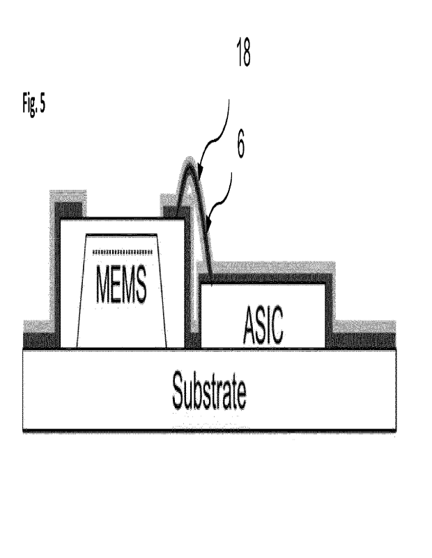
Figure 5 shows a package which is preferably fully surface conformal, in which
a fully surface
conformal coating system 18 is produced by means of vapor phase deposition of
a polymer (e.g.
Parylene). It shows how close-fitting a layer system produced in this way is,
in which even the
structure of the wire bond 6 is retained after coating in the package 14.
26
CA 03182872 2022- 12- 14
LIST OF REFERENCE SIGNS
1 MEMS element, for example MEMS transducer
2 MEMS device
3 MEMS interaction region, for example MEMS membrane.
4 Substrate
Processor, preferably integrated circuit (IC)
6 Electrical connection, preferably wire bond
7 Surface conformal coating (e.g. spray coating)
8 Dielectric layer
9 Electrically conductive layer
Outer edge of the coating
11 Opening in front of the MEMS interaction region, preferably
sound port
12 Sacrificial layer of the non-released interaction region, for
example, of a non-exposed
membrane
13 Back volume
14 MEMS package, for example MEMS transducer package
Released MEMS interaction region, for example, released MEMS membrane
16 Layer system
17 Package environment
18 Surface conformal layer system
27
CA 03182872 2022- 12- 14
LITERATURE
Alfons Dehe, Martin Wurzer, Marc Fuldner and Ulrich Krumbein, The lnfineon
Silicon MEMS
Microphone, AMA Conferences 2013 - SENSOR 2013, OPTO 2013, IRS 22013.
Gregor Feiertag, Wolfgang Pahl, Matthias Winter, Anton Leidl, Stefan Seitz,
Christian Siegel,
Andreas Beer, Flip chip MEMS microphone package with large acoustic reference
volume, Proc.
Eurosensors XXIV, September 5-8, 2010, Linz, Austria.
M. Harth, D. W. Schubert, Simple Approach for Spreading Dynamics of Polymeric
Fluids. In:
Macromol. Chem. Phys. 213, no. 6, March 2012, pp. 654-665.
28
CA 03182872 2022- 12- 14