Note: Descriptions are shown in the official language in which they were submitted.
CA 03182896 2022-10-17
WO 2021/216673 PCT/US2021/028347
MULTI-MATERIAL FIBERS AND METHODS OF MANUFACTURING THE SAME
Statement Regarding Federally Sponsored Research or Development
[0001] This invention was made with U.S. Government support under Agreement
Number W15QKN-16-3-0001 awarded by the Army Contracting Command ¨ New Jersey
(ACC-NJ). The Government has certain rights in the invention.
Cross-Reference To Related Application
[0002] This application claims priority to and the benefit of United States
Provisional
Patent Application Number 63/015,109 filed on April 24, 2020, the disclosure
of which is
incorporated herein by reference in its entirety.
Field of the Invention
[0003] Embodiments of the present invention relate generally to the field
of drawing
multi-material fibers from a preform material and, more specifically, to
methods of drawing
multi-material fibers for use in textiles and garments.
Background of the Invention
[0004] The incorporation of semiconductor technology within fibers,
producing multi-
material fibers, promises to revolutionize the textile market, converting
traditional fibers,
filaments, yarns, and the like into sophisticated devices. These multi-
material fibers can
endow the textiles into which they are intertwined with functions that may
yield services to
the end-user.
[0005] Conventional media for communication of data include wireless
communication
systems (e.g., WiFi), vacuum or fiber optic cable systems, hard-wired (cable)
communication
systems, and the like. The abundance of communication devices operating in and
thereby
saturating the radiofrequency (RF) domain demonstrates a need for new
communication
media. Advantageously, free space optical (FSO) communication provides a
communication
medium offering secure, line-of-sight (LoS), high-bandwidth data transmission
to send
information from one location to another using light.
¨ 1 ¨
CA 03182896 2022-10-17
WO 2021/216673
PCT/US2021/028347
[0006] More specifically, FS() communication propagates electromagnetic
(EM)
radiation through the air wherever light can travel, but only where light can
travel.
Advantageously, optical wireless communication systems operate in the visible
to near infra-
red (NIR) portion of the light spectrum, which offers 104 times more bandwidth
compared to
the RF region of most wireless communication systems.
[0007] Until recently, the fusion of FS() technology with textiles, e.g.,
wearable
garments, has been negligible. However, because the average human body
provides 1.5 to 2
square meters of surface area, which is fertile space for receiving FS0
signals, especially in
the context of LoS communications, opportunities for such fusion exist.
[0008] As multi-material fibers are developed, a prerequisite for
successful
productization of the technology is the development of reliable, robust,
functional fibers that
are capable of surviving the rigors of typical textile use cases. For example,
over their usable
life, all textiles, including those that contain multi-material fibers, should
be capable of
undergoing significant mechanical and environmental abuse (e.g., bending,
stretching,
twisting, machine washing, exposure to sunlight, exposure to temperature
changes, and so
forth) that expose the textile to a myriad of force types (e.g., tension,
compression, torsion,
and so forth). Conventional multi-material fibers are limited in their
abilities to withstand
these stimuli.
[0009] Indeed, in developing multi-material fibers, the textile industry
has learned that
standard thermoplastics, cross-sectional architectures, and internal
electrical and electronic
connection strategies cannot produce fibers with adequate reliability with
respect to, for
example, bend testing, machine washing, fabric incorporation, and/or use case
survivability.
Moreover, the incorporation of semiconductor devices at the preform
fabrication stage may
affect the resulting multi-material fiber by: limiting control over the
location of the devices
at the fiber level, reducing the density of devices per unit length that can
be incorporated in
the fibers, and/or restricting the types of cladding material(s) that can be
used. These
limitations may lead to lower yields as the number of connections between
multi-material
fibers intertwined in the textile increases.
[0010] Accordingly, a need exists for improved multi-material fibers and
methods of
manufacturing the same.
¨2¨
CA 03182896 2022-10-17
WO 2021/216673 PCT/US2021/028347
Summary of the Invention
[0011] In a first aspect, embodiments of the present invention relate to a
method of
manufacturing a multi-material fiber having one or more electrically-
connectable devices. In
some embodiments, the method may include the steps of: positioning each
electrically-
connectable device within a corresponding pocket provided in a preform
material; positioning
a first electrical conductor longitudinally within a first conduit provided in
the preform
material; and drawing the multi-material fiber by causing the preform material
to flow, such
that the first electrical conductor extends within the multi-material fiber
along a longitudinal
axis thereof and makes an electrical contact with a first electrode located on
each electrically-
connectable device. In pertinent part, a metallurgical bond may be formed
between the first
electrical conductor and the first electrode while drawing the multi-material
fiber and/or, after
drawing the multi-material fiber, the first electrical conductor may be
located substantially
along a neutral axis of the multi-material fiber. Alternatively, after drawing
the multi-
material fiber, the connection between the first electrical conductor and the
first electrode of
each electrically-connectable device may be located substantially along the
neutral axis of the
multi-material fiber.
[0012] In further applications, the method may include positioning a second
electrical
conductor longitudinally within a second conduit provided in the preform
material and
drawing the multi-material fiber by causing the preform material to flow, such
that the second
electrical conductor extends within the multi-material fiber along the
longitudinal axis thereof
and makes an electrical contact with a second electrode located on each
electrically-
connectable device. Advantageously, during the drawing, a metallurgical bond
may be
formed between the second electrical conductor and the second electrode
and/or, after
drawing the multi-material fiber, the second electrical conductor may be
located substantially
along the neutral axis of the multi-material fiber. Alternatively, after
drawing the multi-
material fiber, the connection between the second electrical conductor and the
second
electrode of each electrically-connectable device may be located substantially
along the
neutral axis of the multi-material fiber.
[0013] In some implementations, positioning the first electrical conductor
may include
positioning a copper alloy wire (e.g., a copper wire with a silver coating)
within the first
conduit. A bonding material (e.g., a metal alloy material such as a tin-
bismuth solder) may
be deposited on the first electrode prior to drawing the multi-material fiber.
Preferably, the
¨3¨
CA 03182896 2022-10-17
WO 2021/216673 PCT/US2021/028347
melting point of the bonding material substantially matches a glass transition
temperature of
the preform material. In some variations, depositing the bonding material on
the first
electrode utilizes a hot press device.
[0014] In further implementations, the method may also include one or more
of the
following: controlling an aspect ratio (e.g., to be between about 1.1:1 and
about 2.7:1) of the
drawn multi-material fiber; overcoating the drawn multi-material fiber (e.g.,
using a
thermoplastic elastomer material as an overcoat); positioning a support wire
longitudinally
within an additional conduit in the preform material to provide mechanical
stability to each
electrically-connectable device, such that, after the multi-material fiber is
drawn, the support
wire contacts each electrically-connectable device without making electrical
contact with the
first electrical conductor or the first electrode; and positioning one or more
outer wires
longitudinally within a corresponding conduit in the preform material, so
that, after drawing
the multi-material fiber, each outer wire may be located substantially along
the neutral axis of
the drawn multi-material fiber. In some variations, controlling the aspect
ratio may include
adding sidewalls to the drawn multi-material fiber. Sidewalls may be made of
materials that
are any one of: the same as the preform material, materials having the same or
substantially
the same glass transition temperature as the preform material but having other
mechanical
properties that differ, and the like. Advantageously, the twisting behavior
can be better tuned
(e.g., against twisting behavior) if the sidewalls have the same or
substantially the same glass
transition temperature of the preform material but have other mechanical
properties that
differ.
[0015] In some embodiments, the method may also include interlacing the
drawn multi-
material fiber with additional fibers to form a textile. In some applications,
the method may
include adding rigidity to the textile, for example by one or more of: adding
tubing to the
textile; adding a plurality of stiffeners to the textile; adding a backing to
the textile; and/or
adding a ribbon-cable backing to the textile. In some variations, the method
may further
include wrapping the drawn multi-material fiber with an overwrap (e.g.,
cotton, polyester or
any other textile yarn, high performance filaments, and/or high tensile
strength fibers, such as
aramids, dyneema, basalt fibers, and the like) prior to the interlacing and/or
producing a
composite yarn that includes a high modulus and/or high strength mono- or
multi-filament
yarn placed in parallel with a multi-material fiber and overwrapping the
composite yarn with
similar or other textile yarns.
¨4¨
CA 03182896 2022-10-17
WO 2021/216673
PCT/US2021/028347
[0016] In a second aspect, embodiments of the present invention relate to a
textile that
includes one or more multi-material fibers and additional fibers interlaced
with the multi-
material fiber(s). In some embodiments, the multi-material fiber may include a
cladding
material, an electrically-connectable device (e.g., a photodetector or a
photodiode) disposed
within the cladding material, and a first electrical conductor (e.g., a copper
wire, a copper
wire having a silver coating, a tungsten wire, a high tension wire, or an
extra high tension
wire) disposed within the cladding material and in electrical communication
with a first
electrode on the electrically-connectable device. In pertinent part, the first
electrical
conductor may be in electrical communication with the first electrode via a
first metallurgical
bond whose bonding material (e.g., a metal alloy material, such as a solder
made of tin and
bismuth) has a melting temperature that substantially matches a glass
transition temperature
of the cladding material and/or the first electrical conductor may be located
substantially
along a neutral axis of the multi-material fiber. Alternatively, after drawing
the multi-
material fiber, the connection between the first electrical conductor and the
first electrode of
the electrically-connectable device may be located substantially along the
neutral axis of the
multi-material fiber.
[0017] In some implementations, the multi-material fiber may further
include a second
electrical conductor in electrical communication with a second electrode on
the electrically-
connectable device. The second electrical conductor may be in electrical
communication
with the second electrode via a second metallurgical bond whose bonding
material has a
melting temperature that substantially matches the glass transition
temperature of the
cladding material and/or the second electrical conductor may be located
substantially along
the neutral axis of the multi-material fiber. Alternatively, after drawing the
multi-material
fiber, the connection between the second electrical conductor and the second
electrode of the
electrically-connectable device may be located substantially along the neutral
axis of the
multi-material fiber.
[0018] In some applications, the multi-material fiber may have one or more
of the
following: an aspect ratio between about 1.1:1 and about 2.7:1; an overcoating
(e.g., a
thermoplastic elastomer material); an overwrap (e.g., cotton, polyester or any
other textile
yarn, high performance filaments, and/or high tensile strength fibers, such as
aramids,
dyneema, basalt fibers, and the like), a support wire to provide mechanical
stability to the
device, and/or one or more outer wires (e.g., wires made from aramids,
dyneema, tungsten,
and so forth) that are located substantially along the neutral axis of the
multi-material fiber.
¨5¨
CA 03182896 2022-10-17
WO 2021/216673
PCT/US2021/028347
Alternatively, the multi-material fiber may include a composite yarn that
includes a high
modulus and/or high strength mono- or multi-filament yarn placed in parallel
with the multi-
material fiber and overwrapping the composite yarn with similar or other
textile yarns.
[0019] In a third aspect, embodiments of the present invention relate to a
method of
manufacturing a multi-material fiber having one or more electrically-
connectable devices. In
some embodiments, the method may include the steps of: positioning a first
electrical
conductor longitudinally within a first conduit provided in a preform
material; drawing the
multi-material fiber by causing the preform material to flow; creating one or
more pockets
(e.g., by removing preform material using a laser and/or a milling machine) in
the drawn
multi-material fiber to expose the first electrical conductor; positioning an
electrically-
connectable device within each pocket, such that a first electrode on the
electrically-
connectable device is aligned with the first electrical conductor; forming a
metallurgical bond
between the first electrical conductor and the first electrode; and filling
each pocket with an
encapsulate material or an epoxy to protect the electrically-connectable
device.
[0020] In some implementations, the method may also include positioning a
second
electrical conductor longitudinally within a second conduit provided in the
preform material.
In some variations: a pocket may be created to expose the second electrical
conductor, the
electrically-connectable device may be positioned within the pocket, such that
a second
electrode on the electrically-connectable device is aligned with the second
electrical
conductor, and/or a metallurgical bond between the second electrical conductor
and the
second electrode may be formed.
[0021] In further applications, the method may include one or more of:
minimizing
fluctuation of an outer diameter of the drawn multi-material fiber; coating
the first electrode
with a bonding material before the electrically-connectable device is
positioned within the
pocket; interlacing the drawn multi-material fiber with additional fibers to
form a textile;
removing preform material in a first drawn multi-material fiber in the textile
to expose
electrical conductors of the first drawn multi-material fiber; removing
preform material in a
second drawn multi-material fiber that, in the textile, intersects the first
drawn multi-material
fiber to expose electrical conductors of the second drawn multi-material
fiber; and
interconnecting the electrical conductors of the first drawn multi-material
fiber to the
electrical conductors of the second drawn multi-material fiber. In some
variations,
interconnecting the electrical conductors of the first drawn multi-material
fiber to the
¨6¨
CA 03182896 2022-10-17
WO 2021/216673 PCT/US2021/028347
electrical conductors of the second drawn multi-material fiber includes
inserting one or more
of an interposer or a transposer therebetween.
[0022] In a fourth aspect, embodiments of the present invention relate to a
textile that
includes one or more multi-material fibers and additional fibers interlaced
with the multi-
material fiber(s). In some implementations, the multi-material fiber includes
a drawn
preform material (e.g., a thermoplastic material, a thermoplastic elastomer
(e.g.,
polyetherimide (PEI)), or glass), an electrically-connectable device (e.g., a
photodetector or a
photodiode) disposed within the drawn preform material, and a first electrical
conductor (e.g.,
a copper wire, a copper wire comprising a silver coating, a tungsten wire, a
high tension wire,
or an extra high tension wire) disposed within the drawn preform material and
in electrical
communication with the electrically-connectable device. Preferably, the
electrically-
connectable device and some portion of the first electrical conductor are
disposed in a pocket
filled with a filling material or encapsulant (e.g., a photocured epoxy) to
protect the
electrically-connectable device.
[0023] In some applications, the multi-material fiber may further include a
second
electrical conductor disposed within the drawn preform material and in
electrical
communication with the electrically-connectable device. In some variations, a
first electrode
of the electrically-connectable device is bonded to the first electrical
conductor via a bonding
material and/or the first electrical conductor is located substantially along
a neutral axis of the
multi-material fiber. Alternatively, the connection between the first
electrical conductor and
the first electrode of the electrically-connectable device may be located
substantially along
the neutral axis of the multi-material fiber.
[0024] In some applications, the multi-material fiber may have one or more
of the
following: an aspect ratio between about 1.1:1 and about 2.7:1; an overcoating
(e.g., a
thermoplastic elastomer material); an overwrap (e.g., cotton, polyester or any
other textile
yarn, high performance filaments, and/or high tensile strength fibers, such as
aramids,
dyneema, basalt fibers, and the like), a support wire to provide mechanical
stability to the
device, and/or one or more outer wires (e.g., wires made from aramids,
dyneema, tungsten,
and so forth) that are located substantially along the neutral axis of the
multi-material fiber.
Alternatively, the multi-material fiber may include a composite yarn that
includes a high
modulus and/or high strength mono- or multi-filament yarn placed in parallel
with the multi-
material fiber and overwrapping the composite yarn with similar or other
textile yarns.
¨7¨
CA 03182896 2022-10-17
WO 2021/216673 PCT/US2021/028347
[0025] In a fifth aspect, embodiments of the present invention relate to a
method of
manufacturing a multi-material fiber having one or more electrically-
connectable devices. In
some embodiments, the method includes the steps of: fabricating a core portion
of a
composite preform, encasing the core portion within an outer sheath portion to
form the
composite preform, and thermally drawing the composite preform. In some
implementations,
the core portion includes a core material, one or more electrically-
connectable devices, and
one or more electrical conductors in electrical communication with the
electrically-
connectable devices. In some applications, the core portion and the outer
sheath portion are
manufactured from different materials having substantially similar glass
transition
temperatures. For example, the core portion may be manufactured from a
thermoplastic (e.g.,
a cyclic olefin copolymer (COC)) and the outer sheath portion may be
manufactured from a
thermoplastic elastomer (e.g., an elastomeric-cyclic olefin copolymer (e-
COC)).
[0026] In some variations, fabricating the core portion may include one or
more of:
providing multiple layers of the core material; forming a slot in at least two
of the layers (e.g.,
in a first layer and a second layer); forming a pocket in a third layer
disposed between the
first and second layers; positioning a first electrical conductor in a first
slot in the first layer;
positioning a second electrical conductor in a second slot in the second
layer; positioning an
electrically-connectable device in the pocket in the third layer; and
consolidating the first,
second, and third layers (e.g., using a hot press device ) to form the core
portion. In some
embodiments, encasing the core portion may include: placing the core portion
between first
and second clam shell portions of the outer sheath portion and consolidating
the core portion,
the first clam shell portion, and the second clam shell portion (e.g., using a
hot press device).
In some applications, the method may also include interlacing the drawn multi-
material fiber
with additional fibers to form a textile.
[0027] In a sixth aspect, embodiments of the present invention relate to a
textile. In some
embodiments, the textile includes one or more multi-material fibers and
additional fibers
interlaced with the multi-material fiber(s). In some applications, the multi-
material fiber
includes a composite material, an electrically-connectable device disposed
within the
composite material, and one or more electrical conductors disposed within the
composite
material and in electrical communication with the electrically-connectable
device.
Preferably, the composite material includes a first preform material having a
first glass
transition temperature and a second preform material having a second glass
transition
temperature substantially similar to the first glass transition temperature
and encasing the first
¨8¨
CA 03182896 2022-10-17
WO 2021/216673 PCT/US2021/028347
preform material. In some variations, the electrically-connectable device and
the electrical
conductor(s) are disposed in the first preform material.
[0028] In a seventh aspect, embodiments of the present invention relate to
a method of
manufacturing a multi-material fiber having one or more electrically-
connectable devices. In
some embodiments, the method may include the steps of: thermally drawing a
core preform,
manufactured from a first material (e.g., thermoplastic polycarbonate), at a
first temperature
to produce a first drawn fiber; inserting the first drawn fiber within a
hollow portion of a
second preform to form a composite preform, wherein the second preform is
manufactured
from a second material (e.g., an elastomeric-cyclic olefin copolymer (e-COC))
that differs
from the first material; and thermally drawing the composite preform at a
second temperature
to provide the multi-material fiber. In some implementations, the glass
transition temperature
of the second preform is less than the glass transition temperature of the
core preform and/or
the second temperature is less than the glass transition temperature of the
core preform. In
some applications, the first drawn fiber includes one or more electrically-
connectable devices
and one or more electrical conductors in electrical communication with the
electrically-
connectable device(s). In some variations, the method may also include
interlacing the multi-
material fiber with a plurality of additional fibers to form a textile.
[0029] In an eighth aspect, embodiments of the present invention relate to
a textile. In
some embodiments, the textile includes one or more multi-material fibers and
additional
fibers interlaced with the multi-material fiber(s). In some implementations,
the multi-
material fiber includes a composite material, an electrically-connectable
device disposed
within the composite material, and one or more electrical conductors disposed
within the
composite material and in electrical communication with the electrically-
connectable device.
Preferably, the composite material is manufactured from a first preform
material and a second
preform material encasing the first preform material, wherein the first
preform material has a
first glass transition temperature and the second preform material has a
second glass
transition temperature that is less than the first glass transition
temperature. In some
variations, the electrically-connectable device and the electrical
conductor(s) are disposed in
the first preform material.
[0030] These and other objects, along with advantages and features of the
embodiments
of the present invention herein disclosed, will become more apparent through
reference to the
following description, the accompanying drawings, and the claims. Furthermore,
it is to be
¨9¨
CA 03182896 2022-10-17
WO 2021/216673
PCT/US2021/028347
understood that the features of the various embodiments described herein are
not mutually
exclusive and can exist in various combinations and permutations.
Brief Description of the Drawings
[0031] In the drawings, like reference characters generally refer to the
same parts
throughout the different views. Also, the drawings are not necessarily to
scale, emphasis
instead generally being placed upon illustrating the principles of the
invention. In the
following description, various embodiments of the present invention are
described with
reference to the following drawings, in which:
[0032] FIG. 1A shows a schematic of a preform assembly in accordance with
some
embodiments of the present invention;
[0033] FIG. 1B shows a schematic of a preform-to-fiber draw process in
accordance with
some embodiments of the present invention;
[0034] FIG. 2 shows a flow chart of a first method of manufacturing a multi-
material
fiber in accordance with some embodiments of the present invention;
[0035] FIG. 3 shows a schematic of tensile and compressive failure modes of
a member
subjected to bending;
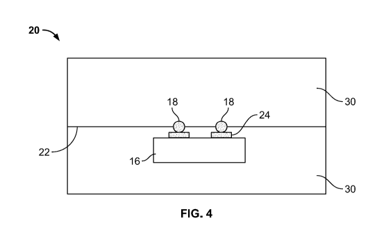
[0036] FIG. 4 shows a cross section of a drawn multi-material fiber having
a high aspect
ratio and electrical conductors located at the neutral axis of the drawn multi-
material fiber in
accordance with some embodiments of the present invention;
[0037] FIG. 5 shows a cross section of a drawn multi-material fiber having
a high aspect
ratio, electrical conductors located at the neutral axis of the drawn multi-
material fiber, and
sidewalls in accordance with some embodiments of the present invention;
[0038] FIG. 6 shows a cross section of a drawn multi-material fiber having
a high aspect
ratio and electrical conductors and outer wires located at the neutral axis of
the drawn multi-
material fiber in accordance with some embodiments of the present invention;
[0039] FIG. 7 shows a schematic of a cross-section of a yarn including a
drawn multi-
material fiber with a high-tensile strength fiber (e.g., aramids, dyneema,
basalt, and the like)
overwrapping in accordance with some embodiments of the present invention;
[0040] FIG. 8 shows a flow chart of a second method of manufacturing a
multi-material
fiber in accordance with some embodiments of the present invention;
¨ 10¨
CA 03182896 2022-10-17
WO 2021/216673 PCT/US2021/028347
[0041] FIG. 9 shows a schematic of an apparatus for performing the second
method of
manufacturing a multi-material fiber depicted in FIG. 8 in accordance with
some
embodiments of the present invention;
[0042] FIG. 10 shows an exemplary garment-level solution for limiting
bending of a
textile in accordance with some embodiments of the present invention;
[0043] FIG. 11 shows a flow chart of a first method of manufacturing a
composite multi-
material fiber in accordance with some embodiments of the present invention;
[0044] FIG. 12A shows a schematic of a core portion and two clam shell
portions for
manufacturing a composite multi-material fiber in accordance with some
embodiments of the
present invention;
[0045] FIG. 12B shows a schematic of the core portion installed in a
central channel
portion of one of the clam shell portions from FIG. 12A in accordance with
some
embodiments of the present invention;
[0046] FIG. 12C shows a schematic of the consolidation of the core portion
and the two
clam shell portions from FIG. 12B in accordance with some embodiments of the
present
invention;
[0047] FIG. 13A shows a schematic of a composite preform having a layered
core portion
encased in an outer shield for manufacturing a multi-material fiber in
accordance with some
embodiments of the present invention;
[0048] FIG. 13B shows a composite multi-material fiber schematic resulting
from
thermally drawing the composite preform of FIG. 13A in accordance with some
embodiments of the present invention;
[0049] FIG. 14 shows a flow chart of a second method of manufacturing a
composite
multi-material fiber in accordance with some embodiments of the present
invention;
[0050] FIG. 15A shows an image of a hollow thermoplastic elastomer (TPE)
preform for
use in the method of FIG. 14 in accordance with some embodiments of the
present invention;
[0051] FIG. 15B shows an image of a drawn multi-material fiber within a
substantially
round hollow TPE preform for use in the method of FIG. 14 in accordance with
some
embodiments of the present invention; and
¨ 11 ¨
CA 03182896 2022-10-17
WO 2021/216673 PCT/US2021/028347
[0052] FIG. 15C shows an image of a drawn multi-material fiber within a
substantially
rectangular hollow TPE preform for use in the method of FIG. 14 in accordance
with some
embodiments of the present invention.
Detailed Description
[0053] Preform-to-Fiber Draw Process
[0054] Multi-material fibers may be drawn using standard thermoplastic draw
techniques,
such that a plurality of semiconductor devices may be embedded in a single
(e.g., drawn)
fiber. Although the invention will be described in connection with multi-
material fibers
manufactured be a draw-down process, that is done for the purpose of
illustration, rather than
limitation. For example, as an alternative to a drawn fiber, the invention may
use electronic
strips that are not drawn. In some embodiments, the draw process includes
preparing or
assembling a preform and then thermally drawing the fiber from the preform.
For example,
in some applications, to prepare the preform, a rectangular or square preform
may be
assembled using sheets and bars of a thermoplastic material that, preferably,
satisfies optical
and mechanical specifications of the end application. Exemplary thermoplastic
materials for
the preform may include, for the purpose of illustration and not limitation:
polycarbonate
(PC), polyarylsulfones (PSU), polyetherimide (PEI), polyethylene terephthalate
(PET), cyclic
olefin copolymer (COC), and the like. In a process known as consolidation, the
component
pieces of the preform may be stacked together and heated (e.g., to a glass
transition
temperature of the preform material) using a hot press or similar device in
order to fuse, by
heat and pressure, the various layers together.
[0055] Prior to or while a preform is being assembled, the components of
the preform
may be cleaned and moisture removed. Moisture may be removed from the preform
components in advance of preform assembly by drying in a vacuum oven at
elevated
temperature for 1-2 weeks.
[0056] In a next step, the preform may be mounted to a draw tower within,
for example, a
three-zone furnace; spools containing electrical conductors and other wire(s)
may be disposed
above the draw tower. In the draw tower, the thermoplastic material of the
preform may be
heated (e.g. at or near its glass transition temperature (TO) until it begins
to flow under the
force of the weight or mass body attached to the bottom of the preform. As the
fiber is drawn
from the preform, each of the elongate wires on the spools align with
semiconductor devices,
¨ 12¨
CA 03182896 2022-10-17
WO 2021/216673 PCT/US2021/028347
such that, in some applications, a plurality of (e.g., two) electrical
conductors physically
contact an obverse face of the semiconductor device, and, advantageously
create an electrical
communication with respective electrodes on the semiconductor device.
Optionally, a third
wire (and/or additional wires) maybe drawn so as to physically contact the
reverse face of the
semiconductor without establishing any electrical contact. Contact between the
two electrical
conductors against the obverse face and the third wire against the reverse
face captures the
semiconductor device between the three elongate wires, supporting the
semiconductor device
within the drawn fiber.
[0057] Once a fiber emerges from the furnace it may be attached to a
capstan/winder
system, which winds the drawn fiber at a controlled rate. The temperature of
the furnace
coupled with the winding rate and the rate at which the preform is lowered
into the furnace
controls the overall diameter of the fiber.
[0058] More particularly, referring to FIGS. 1A and 1B, during multi-
material fiber
manufacture, a (e.g., thermoplastic) preform 10 maybe heated to or near its
glass transition
temperature (TO as the preform 10 is systematically drawn to produce a drawn
fiber 20.
[0059] Advantageously, prior to the drawing activity, a plurality of slots
12 and a
plurality of conduits 14 may be formed in the preform 10; semiconductor
devices 16 may be
inserted into the slots 12 and electrical conductors 18, as well as other
wires, may be inserted
in the conduits 14. Conduits 14 for the electrical conductors 18 (and other
wires) may be
slot-milled through the longitudinal length of the preform 10. In some
variations, to prevent
a conduit(s) 14 from collapsing during subsequent consolidation steps, a
(e.g., PTFE) tube
may be inserted into the conduit(s) 14. Once the conduit(s) 14 have been
prepared, any
inserted tube(s) may be removed and electrical conductors 18 (and other wires)
installed in or
passed through each conduit(s) 14.
[0060] As the preform 10 is drawn, the electrical conductors 18 (and other
wires) may be
fed into the preform 10 whose form is increasing axially and decreasing
radially. As the
cross-sectional dimensions continue to decrease, the distance between the
electrical
conductors 18 (and other wires) and the semiconductor devices 16 also
decreases, until the
distance between the semiconductor devices 16 and the electrical conductors 18
(and other
wires) is less than about the thickness of the semiconductor devices 16. When
this occurs,
the electrical conductors 18 (and other wires) are in physical contact with
the semiconductor
devices 16 and, more preferably, each of the electrical conductors 18 is in
physical contact
¨ 13 ¨
CA 03182896 2022-10-17
WO 2021/216673 PCT/US2021/028347
with a respective electrode 24 (FIG. 4) on the semiconductor devices 16,
completing an
electrical circuit.
[0061] Advantageously, this fiber draw process is capable of manufacturing
multi-
material fibers 20 having a plurality of semiconductor devices 16 connected in
parallel.
Mechanical bonds or connections between the electrical conductors 18 and the
electrodes 24
on each of the semiconductor devices 16 provide electrical communication
therebetween.
Since the bonds are only mechanical in nature, in some instances, small
mechanical forces
applied to the semiconductor devices 16 and/or to the electrical conductors 18
may cause the
electrical connections to fail. Hence, incorporation of multi-material fibers
20 into a textile
via conventional machine integration that applies mechanical forces to the
multi-material
fibers 20 (e.g., by weaving, by knitting, and the like) may be difficult.
Moreover, multi-
material fibers 20 may fail in use cases that include bending motion (e.g.,
washing, drying,
and the like). Heretofore, mechanical connections between electrical
conductors 18 and
electrodes 24 on semiconductor devices 16 were used exclusively in the preform-
to-fiber
draw process. Indeed, due to the nature of the preform-to-fiber draw process,
metallurgical
bonds were unknown.
[0062] Formation of Metallurgical Bonds During the Fiber Draw Process
[0063] Referring to FIGS. 2 and 4, a method of manufacturing a multi-
material fiber 20
via a preform-to-fiber draw process that includes metallurgical bonding
electrical conductors
18 to electrodes 24 on the semiconductor devices 16 during the drawn-down
process is
shown. In a first step, the process includes depositing a low-melting point
bonding material,
e.g., a metal alloy solder such as a tin:bismuth solder containing about 48
percent tin and
about 52 percent bismuth (485n:52Bi), onto the electrodes 24 of the
semiconductor devices
16 (STEP 1). Preferably, the melting temperature (MP) of the bonding material
is matched to
the glass transition temperature (TO of the preform material, such that the
heat used to
thermally draw the preform 10 is also sufficient to raise the temperature of
the bonding
material to its melting point, which produces a metallurgical bond when the
electrical
conductors 18 converge on the electrodes 24 of the semiconductor devices 16.
[0064] In some implementations, a hot press may be used to deposit (e.g.,
about 2-10
microns of) the bonding material on the electrodes 24. To prevent potential
shorting of the
semiconductor devices 16, application of the bonding material should be
controlled to contain
the deposited bonding material proximate the respective electrodes 24. For
example, if a hot
¨ 14¨
CA 03182896 2022-10-17
WO 2021/216673 PCT/US2021/028347
press is used to deposit the bonding material, the vertical (or z-travel)
displacement of the
dispensing nozzle of the hot press may be limited to prevent displacement of
the bonding
material.
[0065] Prior to fiber drawing, a plurality of pockets 12 (STEP 2A) and a
plurality of
conduits 14 (e.g., two) (STEP 2B) may be formed in the preform 10, so as to
ensure
convergence of the electrical conductors 18 onto respective electrodes 24 on
the
semiconductor devices 16. Pockets 12 for the semiconductor devices 16 may be
end-milled
in the upper face of the preform 10 at discrete locations.
[0066] Semiconductor devices 16 may then be inserted in each of the pockets
12 (STEP
3A) and electrical conductors 18 may be inserted in each of the conduits 14
(STEP 3B).
Centering the semiconductor devices 16 within the pockets 12 formed in the
preform 10 with
respect to the electrical conductors 18 may prevent smearing of the bonding
material during
convergence, i.e., when the electrical conductors 18 converge onto the
electrodes 24 of the
semiconductor devices 16. In some variations, the electrical conductors 18 may
be
manufactured of copper or tungsten. For stronger bond formation, an extra-high
tension wire,
e.g., a silver-coated copper alloy wire, such as XHTW manufactured by
Elektrisola GmbH &
Co. KG of Reichshof-Eckenhagen, Germany, may be used.
[0067] Location of Electrical Conductors at the Neutral Axis of the Drawn
Fiber
[0068] Failure due to breakage of the electrical conductors 18 and/or
breakage of the
electrical contact between the electrical conductors 18 and the electrodes 24
of the
semiconductor devices 16 (e.g., due to ordinary wear and tear, during washing,
drying, and
the like) can be a leading mode of failure of the multi-material fiber 20.
More specifically, as
shown in FIG. 3, as the multi-material fiber 20 is subjected to or undergoes
bending, a
portion of the multi-material fiber 20 and the electrical conductors 18 is
compressed and
another portion of the multi-material fiber 20 and the electrical conductors
18 is placed in
tension. The portion of the multi-material fiber 20 in tension causes the
electrical conductors
18 to elongate, introducing a defect in the electrical conductors 18, which,
with repeated
bending, weakens the electrical conductors 18 and the multi-material fiber 20.
Bending may
also affect the metallurgical bonds that experience a touch sensitivity that
can cause
deterioration or breakage of the bond between the electrical conductors 18 and
the electrodes
24. Ultimately, repeated bending may cause the electrical conductors 18 to
break or the bond
between the electrical conductors 18 and the electrodes 24 to deteriorate.
¨ 15 ¨
CA 03182896 2022-10-17
WO 2021/216673
PCT/US2021/028347
[0069] To address the mode of failure due to bending electrical conductors
18, the fiber
draw process may be adapted. For example, conduits 14 in the preform 10 may be
prepared
(STEP 2B) and electrical conductors 18 may be installed in the conduits 14 in
the preform 10
(STEP 3B), such that, as shown in FIGS. 3 and 4, at the completion of the
fiber draw-down
process, the electrical conductors 18 are located at or near the neutral axis
22 of the multi-
material fiber 20 (STEP 4). Alternatively, after drawing the multi-material
fiber, the
connection between the electrical conductors 18 and the corresponding
electrodes 24 of the
electrically-connectable device 16 may be located substantially along the
neutral axis 22 of
the multi-material fiber 20. By prearranging the electrical conductors 18 and
drawing down
the preform 10 so that, at convergence, the electrical conductors 18 rest at
or near the neutral
axis 22 of the drawn multi-material fiber 20 (STEP 4) or, in the alternative,
the connections
between the electrical conductors 18 and the corresponding electrodes 24 of
the electrically-
connectable device 16 are located substantially along a neutral axis 22 of the
multi-material
fiber 20, the compressive or tensile forces acting on the electrical
conductors 18 are
minimized. Indeed, the extent to which electrical conductors 18 or, in the
alternative, the
extent to which the connections between the electrical conductors 18 and the
corresponding
electrodes 24 of the electrically-connectable device 16 would be subject to
compressive or
tensile forces is proportional to the distance of the electrical conductors 18
(or the
connections) from the neutral axis 22. Hence, the closer the electrical
conductors 18 ¨ and,
more specifically, the central axis of the electrical conductors 18 ¨ or, in
the alternative, the
closer the connections between the electrical conductors 18 and the
corresponding electrodes
24 of the electrically-connectable device 16 are to the neutral axis 22 of the
multi-material
fiber 20, the less the electrical conductors 18 (or the connections) are
subjected to the
deleterious effects of repeated compression or tension.
[0070] Although positioning the electrical conductors 18 (or the
connections), after
convergence, at or near the neutral axis 22 of the drawn multi-material fiber
20 (STEP 4)
makes the drawn multi-material fiber 20 more robust and survivable, this is
only true in a
single plane that subjects the drawn multi-material fiber 20 to tensile and
compressive loads.
Thus, to address the stresses and strains that may be generated when the drawn
multi-material
fiber 20 is subject to torsion, the drawn multi-material fiber 20 may be
designed to have a
relatively high (e.g., 1.1:1 to 2.7:1) aspect ratio (STEP 5) of the width (W)
of the drawn
multi-material fiber 20 to the height (H) of the drawn multi-material fiber
20. By increasing
the aspect ratio (STEP 5), out-of-plane torsion and other forces will not
expose the electrical
¨ 16¨
CA 03182896 2022-10-17
WO 2021/216673 PCT/US2021/028347
conductors 18 to out-of-plane tension. The relatively high aspect ratio (as
shown in FIG. 4)
may be provided in the design of the multi-material fiber 20, so that as the
multi-material
fiber 20 is drawn, the resulting multi-material fiber 20 is somewhat
elliptical, rectangular, or
oval, so as to have a longer width than a height. In the alternative, as shown
in FIG. 5,
additional sidewalls 24 may be attached, adhered, or bonded to the drawn multi-
material fiber
20 (STEP 5) to ensure that the width of the multi-material fiber 20 is greater
than its height.
[0071] Optionally, as shown in the multi-material fiber 20' illustrated in
FIG. 6, to further
restrict bending along the neutral axis 22 plane, i.e., torsion, outer (e.g.,
structural) wires 26
may be incorporated in the preform 10 (STEP 6) during the thermal draw
process. In some
embodiments, each outer (e.g., structural) wire 26 may be a high tension wire
(e.g., wires
made from aramids, dyneema, tungsten, and so forth) that is installed in a
corresponding
conduit 14 in the preform 10, such that, after the multi-material fiber 20'
has been thermally
drawn, each outer (e.g., structural) wire 26 is located at or near the neutral
axis 22 of the
drawn multi-material fiber 20', between the outer surface 28 of the drawn
multi-material fiber
20' and a corresponding electrical conductor 18.
[0072] Environmental Barriers and Yarn Wrapping for Drawn Fibers
[0073] Due to the brittle nature of most thermoplastics, kinking may occur
when the
multi-material fiber 20 is bent beyond a critical radius of curvature. Kinking
produces strains
in the thermoplastic material or cladding 30 that surrounds and encases the
devices 16 and the
electrical conductors 18. Through fatigue due to kinking, the cladding 30 may
develop local
defects, which can lead to failure of the multi-material fiber 20'. Since the
thermoplastic
cladding 30 about the electrical conductors 18 provides resistance against
bending, if the
cladding 30 fails, over time, the electrical conductors 18 and/or the
electrical connections
between the electrical conductors 18 and the electrodes 24 are also likely to
fail.
Accordingly, in a next step, the cladding 30 may be encased in an (e.g.,
thermoplastic
elastomer) overcoating 32 (STEP 7) that is structured and arranged to prevent
the multi-
material fiber 20 from bending beyond a point that would otherwise lead to
kinking without
reducing the bend radius of the multi-material fiber 20'. Exemplary
overcoating materials 32
include, for the purpose of illustration rather than limitation: polyester.
[0074] Crazing is a process by which thermoplastics fail due to the
migration of a solvent
(e.g., water) into the cladding 30 matrix. For example, through fatigue caused
by repeated or
cyclical kinking, tension cracks may appear in the surface of the cladding 30,
providing a
¨ 17¨
CA 03182896 2022-10-17
WO 2021/216673 PCT/US2021/028347
means of ingress for solvents. Solvent migration within the cladding 30 matrix
locally
weakens (at the point of migration) the polymer, leading to stress cracking
and failure. In
order to prevent ingress of solvents into the thermoplastic cladding 30, the
cladding 30 may,
optionally, be coated with a hydrophobic, thermoplastic elastomer barrier
material 32 (STEP
7).
[0075] As multi-material fibers 20 are intertwined with other fibers, e.g.,
using a machine
or other mechanical means, to produce a fabric or textile (e.g., by weaving,
knitting, and so
forth), the multi-material fibers 20 may be subjected to large tensile forces.
To mitigate these
large tensile forces, as shown in FIG. 7, the multi-material fibers 20 may be
wrapped with
high-tensile strength (e.g., aramids, dyneema, basalt, and the like) fibers 34
to provide a yarn
36 having an extremely high-tensile strength (STEP 8). The yarn 36, in turn
may be
overcoated with a (e.g., polyester) material 38. In some applications, the
multi-material fiber
may include a composite yarn that includes, for example, a high modulus and/or
high strength
mono- or multi-filament yarn placed in parallel with the multi-material fiber.
Advantageously, the composite yarn may be overwrapped with similar or other
textile yarns.
[0076] Post-Draw Placement of Semiconductor Devices
[0077] Incorporation of semiconductor devices into the preform material
prior to the
thermal draw process may, in some instances, affect the accuracy of
semiconductor location
at the fiber level. Moreover, with pre-draw placement of semiconductor
devices, the density
of devices may be severely limited by the draw-down ratio. As a result, in
some instances, as
shown in FIGS. 8 and 9, it may be preferable to manufacture a multi-material
fiber 20" by,
first, drawing the (e.g., PEI, borosilicate glass, and so forth) fiber 20"
with appropriate
electrical conductor geometries (STEP 1') and then, once drawn, installing the
semiconductor
devices 16" at desired locations (STEP 2'), which, advantageously, may include
devices 16'
that are placed adjacent to one another.
[0078] While thermally-drawing the multi-material fiber 20" from the
preform material
10", the tension on the electrical conductors 18 and other wires 26 should be
balanced and it
is important, if not critical, that the preform material 10" should remain
centered within the
furnace 40 during draw-down. For the milling process used to create pockets 50
in the drawn
multi-material fiber 20", care should be taken in the drawing process to
minimize fluctuation
of the outer diameter (OD) of the drawn fiber 20".
¨ 18¨
CA 03182896 2022-10-17
WO 2021/216673
PCT/US2021/028347
[0079] More specifically, the drawn multi-material fiber 20" may be
modified (e.g.,
using a laser, a (e.g., CNC end-) milling machine, and the like) to
selectively remove
cladding material 30 from the drawn fiber 20" (STEP 2A'). Doing so forms a
pocket 50 at
discrete locations in the drawn multi-material fiber 20", so as to expose the
electrical
conductors 18 and other wires 26 that are, preferably, disposed at the neutral
axis of the
multi-material fiber 20".
[0080] With the electrical conductors 18 and other wires 26 exposed, the
electrodes of a
semiconductor device 16" may be placed against and metallurgically-bonded
(e.g., by
heating each solder-coated electrode with a soldering iron) to corresponding
electrical
conductors 18 (STEP 2B'). Advantageously, the post-draw creation of pockets 50
in the
drawn multi-material fiber 20" makes it easier to appropriately and correctly
align the
semiconductor device 16" vis-à-vis the electrical conductors 18. Those of
ordinary skill in
the art can appreciate that, due to the post-draw soldering operation, the
preform (i.e.,
cladding) material 30 should be selected so that the glass transition
temperature of the
preform (i.e., cladding) material 30 is greater than the melting point of the
bonding material.
Once the electrodes of the semiconductor device 16" have been metallurgically-
bonded to
the electrical conductors 18, a filling material or encapsulant 52 (e.g., a
photocurable epoxy)
may then be placed in the pocket 50 and (e.g., ultraviolet (UV)) cured (STEP
2C') to protect
the underlying semiconductor device 16" and electrical conductors 18. The
filling material
52 hardens or sets depending on the composition of the encapsulate. For
example, a
photocured epoxy may be used in connection with light curing and transfer
molding.
[0081] In order to fabricate a textile that includes, for example, circuit
boards, local
interconnections between multi-material fibers 20" may be formed (STEP 3') by
selectively
removing cladding material 30 from each of the drawn multi-material fibers 20"
proximate
their point of intersection (STEP 2A'), so as to expose some portion of each
of the electrical
conductors 18. Electrical communication between the exposed portions of each
electrical
conductor 18 may then be effected (STEP 3A') to provide a fiber-to-fiber
connection. In
some applications, one or more of an interposer or a transposer may be
introduced between
the exposed portions of the electrical conductors 18 (STEP 3B'). Once the
exposed portions
of the electrical conductors 18 have been electrically coupled, a filling
material or
encapsulate 52 (e.g., a photocurable epoxy) may then be placed into the area
that was
removed and (e.g., ultraviolet (UV)) cured (STEP 3C') to protect the
electrical conductors 18
and the connection therebetween.
¨ 19¨
CA 03182896 2022-10-17
WO 2021/216673 PCT/US2021/028347
[0082] Once a multi-material fiber(s) 20" has been integrated into a
textile or garment, as
shown in FIG. 10, devices for adding rigidity to the textile or garment (e.g.,
tubing, stiffeners,
backing, and the like) may be incorporated into the textile of garment (STEP
4'). The
devices for adding rigidity limit the bending dynamic making the fabric
stronger.
[0083] Composite Device Fibers
[0084] Thermoplastic polycarbonate (PC) possesses good tensile strength,
optical
transparency, and thermomechanical properties and, hence, is an important
material for
fabricating multi-material fibers. Disadvantageously, however, PC is
relatively rigid; hence,
PC fibers tend to kink when a certain bend radius (e.g., a critical bend
radius) is exceeded.
Kinking may result from plastic deformation due to large tensile strain that
the outermost
portion of the fiber undergoes during bending. Accordingly, in some
embodiments of the
present invention, the multi-material fiber may include a core material
composed of a rigid
thermoplastic material for housing the semiconductor device(s) and electrical
conductors (or
other wires) in combination with an outer sheath composed of a thermoplastic
elastomer
(TPE) material that encases the core material. Because TPE materials typically
have large
elastic moduli and, since the encasing TPE material is located at the points
of highest tensile
and compressive strain, these composites can be reversibly (i.e., elastically)
bent without
plastic deformation.
[0085] While die coating, melt spinning, and other overcoating processes or
techniques
may be used to manufacture such a multi-material fiber, there are particular
advantages of
thermally drawing a composite preform to produce a multi-material fiber.
Moreover, such a
thermal-drawing process may also be used in connection with manufacturing
optical lenses,
interconnects, multi-material sheaths, and so forth.
[0086] Referring to FIG. 11, a flow chart for a first exemplary method of
manufacturing
composite multi-material fibers and, more specifically, (e.g., kink-resistant)
fibers having
complex, three-dimensional architectures is shown. The first process is a co-
drawing process
in which a core material composed of a rigid thermoplastic material and an
outer sheath
composed of a less-rigid, TPE material may be used. In a first step, different
materials for the
core and the outer sheath are selected (STEP 1"). To ensure that the
viscosities of the two
materials will act similarly at a given temperature, a core material and an
outer sheath
material having similar or substantially similar glass transition temperatures
(TO may be
provided (STEP 1"). For example, for the purpose of illustration rather than
limitation, the
¨ 20 ¨
CA 03182896 2022-10-17
WO 2021/216673 PCT/US2021/028347
materials of the composite may include a cyclic olefin copolymer (COC) or PC
for the
thermoplastic core material and an elastomeric-cyclic olefin copolymer (e-COC)
for the TPE
outer sheath.
[0087] Referring to FIGS. 12A-12C and FIGS. 13A and 13B, once the core
material and
outer sheath materials have been decided upon, the former may be used to
fabricate the core
portion 60, which, preferably, is a relatively rigid core portion 60.
Advantageously, a rigid
core portion 60 maintains good mechanical contact between the electrodes of
the
semiconductor devices 72 and the corresponding electrical conductors 74 and
prevents the
non-elastic electrodes and buses from breaking due to excessive strain that
may be caused by
bending the drawn composite fiber 70 in the tensile direction. In some
implementations, the
core portion 60 may be manufactured using a multi-layer approach (STEP 2").
For example,
the core portion shown in FIGS. 13A and 13B includes three layers 62a, 62b,
and 62c: a
central layer 62b, and two outer layers 62a, 62c. As part of the multi-layer
approach (STEP
2"), conduits 64 for receiving the electrical conductors 74 may be milled in
the outer layers
62a, 62c (STEP 2A") and a plurality of pockets 66 for receiving semiconductor
devices 72
may be prepared within the central layer 62b (STEP 2B"). Once the pockets 66
have been
prepared in the central layer 62b (STEP 2B"), semiconductor devices 72 may be
inserted into
the pockets (STEP 2C"). The three layers 62a, 62b, and 62c may then be
assembled and
consolidated (STEP 2D"), e.g., using a hot press machine, so that, after the
consolidation, the
core 60 consists essentially of a single component.
[0088] In a next step, the consolidated core portion 60 may be inserted
within or placed
inside of a more flexible outer sheath 65 (STEP 3") (FIG. 13A). In some
applications, the
outer sheath 65 may include a first clam shell portion 67 and a second clam
shell portion 69
that each include a central channel portion 68 that runs the length of each
clam shell portion
67, 69. Preferably, the shape of the central channel portions 68, when the
clam shell portions
67, 69 are assembled prior to consolidation, is the same or substantially the
same (e.g., oval,
elliptical, round, square, rectangular, and so forth) as one-half of the shape
of the
consolidated core portion 60. Once the consolidated core portion 60 has been
placed in the
central channel portion 68 of the second clam shell portion 69 (STEP 3A"), the
first clam
shell portion 67 may be placed over the exposed portion of the consolidated
core portion 60,
such that the exposed portion of the consolidated core portion 60 is disposed
within the
central channel portion 68 of first clam shell portion 67 (STEP 3B") (FIG.
12C). The
assembled core portion 60 and outer sheath 65 may then be consolidated, e.g.,
using a hot
¨ 21 ¨
CA 03182896 2022-10-17
WO 2021/216673 PCT/US2021/028347
press machine, to produce a composite preform 70 (STEP 4") that may be
thermally drawn
by a fiber draw process to produce a composite, multi-material fiber (STEP
5").
[0089] Alternatively, in a second embodiment of a method of manufacturing a
composite
multi-material fiber, a rigid, multi-material fiber may be drawn in a first
thermal drawing
process and then the drawn multi-material fiber may be inserted into a hollow,
TPE preform,
which combination may then be subjected to a second thermal drawing process.
More
specifically, referring to FIG. 14 and FIGS. 15A-15C, in this alternative
approach, a plurality
of electrical conductors (and other wires) and semiconductor devices may be
installed (using
techniques described herein) in a relatively rigid (e.g., PC) preform material
that is,
subsequently, thermally drawn-down in a first thermal drawing process to
produce a multi-
material (e.g., PC) fiber 80 (STEP 1'). A hollow (e.g., e-COC) preform 85
having a (e.g.,
round, rectangular, and the like) central opening 82 may also be manufactured
(STEP 2"),
such that the dimensions of the central opening 82 are sufficiently large to
enable one to
install the drawn multi-material fiber 80 within the opening 82 and for the
entire length of the
hollow preform 85 (STEP 3'"). Preferably, the glass transition temperature of
the drawn
multi-material fiber 80 is greater than the glass transition temperature of
the hollow preform
85 (e.g., about 70 degrees Centigrade greater) to ensure that, during a second
thermal drawing
process, the dimensions and shape of the drawn multi-material fiber 80 are not
changed by
the heat in the furnace 40.
[0090] The drawn multi-material fiber 80 may then be inserted into and
through the
opening 82 of the hollow preform 85 (STEP 3") as shown in FIGS. 15B and 15C
and the
composite subject to a second thermal drawing process (STEP 4") in which the
furnace
temperature is at or near the glass transition temperature of the hollow
preform 85 but less
than the glass transition temperature of the previously-drawn multi-material
fiber 80.
[0091] Having described certain embodiments of the invention, it will be
apparent to
those of ordinary skill in the art that other embodiments incorporating the
concepts disclosed
herein may be used without departing from the spirit and scope of the
invention.
Accordingly, the described embodiments are to be considered in all respects as
only
illustrative and not restrictive.
¨ 22 ¨