Note: Descriptions are shown in the official language in which they were submitted.
WO 2022/212038
PCT/US2022/020395
SCALABLE CIRCUIT FOR MOLECULAR DETECTION
CROSS-REFERENCE TO RELATED APPLICATIONS
[00011 This application claims priority to U.S.
Provisional Application No.
63/169041, filed March 31, 2021, the content of which is incorporated by
reference in its
entirety.
BACKGROUND
[0002] Some polynucleotide sequencing techniques involve
performing a large
number of controlled reactions on support surfaces or within predefined
reaction chambers.
The controlled reactions may then be observed or detected, and subsequent
analysis may help
identify properties of the polynucleotide involved in the reaction. Examples
of such
sequencing techniques include next-generation sequencing or massive parallel
sequencing
involving sequencing-by-ligation, sequencing-by-synthesis, reversible
terminator chemistry,
or pyrosequencing approaches.
[00031 Some polynucleotide sequencing techniques utilize a
nanopore, which can
provide a path for an ionic electrical current. For example, as the
polynucleotide traverses
through the nanopore, it influences the electrical current through the
nanopore. Each passing
nucleotide, or series of nucleotides, that passes through the nanopore yields
a characteristic
electrical current. These characteristic electrical currents of the traversing
polynucleotide can
be recorded to determine the sequence of the polynucleotide.
[0004] However, state of the art nanopore sequencing
technologies may suffer
from several problems. For example, electrochemical DC current readout of
nanopores is not
scalable to small trans-well volumes. Further, small currents through pores
make for big
amplifiers. Moreover, large bilayer capacitance makes switching readout
difficult.
Furthermore, large resistor-capacitor (RC) transients while bilayer charges or
discharges.
Prior methods may apply a direct current (DC) or square wave input, which
requires waiting
for the transient electrical responses to decay away before reading out the
steady state
signals. Therefore, measuring the ionic current of prior nanopores may
incorrectly be
measuring the RC transient.
-1 -
CA 03183813 2022- 12- 21
WO 2022/212038
PCT/US2022/020395
SUMMARY
100051 Provided in examples herein are systems for
sequencing biopolymers and
methods of using the systems.
100061 In one aspect, disclosed herein is a nanopore
sensor device for identifying
nucleotides. The device may comprise one or more cis wells; one or more cis
electrodes
associated with the one or more cis wells; a plurality of trans wells, each of
the plurality of
trans wells separated from the one or more cis wells by a lipid or solid-state
membrane
having a nanopore; a plurality of field effect transistors (FETs), each of the
plurality of FETs
associated with one of the plurality of trans wells; an electrical source
configured to provide
alternating current (AC) inputs between the one or more cis electrodes and the
source
terminals of the plurality of FETs; and a controller operably coupled to the
plurality of FETs,
the controller configured to measure AC responses of the plurality of FETs,
wherein the AC
responses depend on the identities of the nucleotides within or near the
nanopores. in some
embodiments, the controller is configured to measure changes of the amplitudes
of the AC
responses. In some embodiments, the controller is configured to measure
changes of the
waveform shapes of the A.0 responses. In some embodiments, the electrical
source is
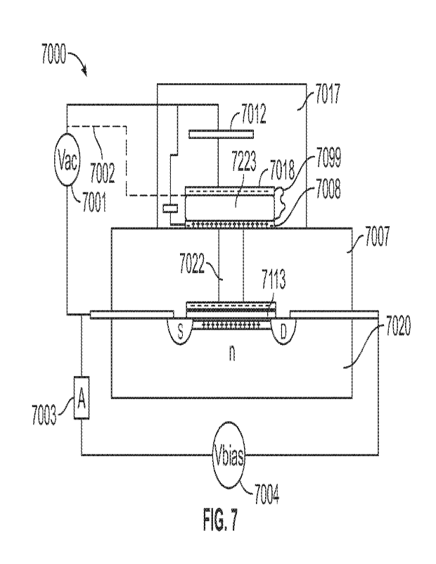
configured to provide an AC voltage in a sinusoidal, rectangular, triangular,
saw-tooth, or
another suitable waveform alternating between a positive potential and a
negative potential.
In some embodiments, the ionic fluxes through the nanopores are modulated by:
nucleotides
passing through the nanopores, labels on nucleotides being incorporated to
polynucleotides,
or any combination thereof.
[0007] In one aspect, disclosed herein is a method of
identifying nucleotides. The
method may comprise providing a nanopore within a membrane separating a cis
well and a
trans well; providing an AC input from an electrical source operably coupled
to a cis
electrode in the cis well and to the source terminal of a FET in the trans
well; and measuring
an AC response from the FET, wherein the AC response depends on the identity
of a
nucleotide within or near the nanopore. In some embodiments, measuring the AC
response
comprises measuring a change of the amplitude of the AC response. In some
embodiments,
measuring the AC response comprises measuring a change of the waveform of the
AC
response. In some embodiments, providing the AC input comprises providing an
AC voltage
in a sinusoidal, rectangular, triangular, saw-tooth, or another suitable
waveform alternating
-2-
CA 03183813 2022- 12- 21
WO 2022/212038
PCT/US2022/020395
between a positive potential and a negative potential. In some embodiments,
measuring the
AC response comprises measuring a first response associated with a first
nucleotide and a
second response associated with a second nucleotide without waiting for a
transient response
to approach a steady-state response.
[0008] In one aspect, disclosed herein is a sensor device
for identifying
nucleotides. The device may comprise an electrode; a FET; a partially double-
stranded
nucleic acid polymer having one end operably coupled to the electrode and the
other end
operably coupled to the gate terminal of the FET; an electrical source
configured to provide
an AC input between the electrode and the source terminal of the FET; and a
controller
operably coupled to the FET, the controller configured to measure an AC
response of the
FET, wherein the AC response depends on the identity of a nucleotide
interacting with the
partially double-stranded nucleic acid polymer. In some embodiments, the
controller is
configured to measure a change of the amplitude of the AC response In some
embodiments,
the controller is configured to measure a change of the waveform shape of the
AC response.
In some embodiments, the electrical source is configured to provide an AC
voltage in a
sinusoidal, rectangular, triangular, saw-tooth, or another suitable waveform
alternating
between a positive potential and a negative potential. In some embodiments,
electrical
conduction through the partially double-stranded nucleic acid polymer is
modulated by a
nucleic acid label on a nucleotide being incorporated to a polynucleotide, the
nucleic acid
label being partially complementary to the partially double-stranded nucleic
acid polymer.
[0009] The systems, devices, kits, and methods disclosed
herein each have
several aspects, no single one of which is solely responsible for their
desirable attributes.
Without limiting the scope of the claims, some prominent features will now be
discussed
briefly. Numerous other examples are also contemplated, including examples
that have
fewer, additional, and/or different components, steps, features, objects,
benefits, and
advantages. The components, aspects, and steps may also be arranged and
ordered
differently. After considering this discussion, and particularly after reading
the section
entitled "Detailed Description," one will understand how the features of the
devices and
methods disclosed herein provide advantages over other known devices and
methods.
[0010] It is to be understood that any features of the
device and/or of the array
disclosed herein may be combined together in any desirable manner and/or
configuration.
-3-
CA 03183813 2022- 12- 21
WO 2022/212038
PCT/US2022/020395
Further, it is to be understood that any features of the method of using the
device may be
combined together in any desirable manner. Moreover, it is to be understood
that any
combination of features of this method and/or of the device and/or of the
array may be used
together, and/or may be combined with any of the examples disclosed herein.
Still further, it
is to be understood that any feature or combination of features of any of the
devices and/or of
the arrays and/or of any of the methods may be combined together in any
desirable manner,
and/or may be combined with any of the examples disclosed herein.
[0011] It should be appreciated that all combinations of
the foregoing concepts
and additional concepts discussed in greater detail below are contemplated as
being part of
the inventive subject matter disclosed herein and may be used to achieve the
benefits and
advantages described herein.
BRIEF DESCRIPTION OF THE DRAWINGS
[0012] Features of examples of the present disclosure will
become apparent by
reference to the following detailed description and drawings, in which like
reference
numerals correspond to similar, though perhaps not identical, components. For
the sake of
brevity, reference numerals or features having a previously described,
function may or may
not be described in connection with other drawings in which they appear.
[0013] FIG. IA, FIG. 1B, FIG. 1C and FIG. 1D schematically
illustrate
embodiments including a nanopore.
[0014] FIG. IE schematically illustrates an example of a
solid-state nanopore.
[0015] FIG. 2A, FIG. 2B, FIG. 2C, FIG. 2D, FIG.. 2E and
FIG. 2F schematically
illustrate embodiments including a tether anchored adjacent to a biological
nanopore.
[0016] FIG. 3A, FIG. 3B and FIG. 3C schematically
illustrate embodiments
including a nanopore formed with ionophores.
[00171 FIG. 4 is a schematic diagram of an example of a
sensing system including
a molecular bridge sensor.
[0018] FIG. 5 is schematic diagram of another example of a
molecular bridge
sensing system.
[0019] FIG. 6 schematically illustrates an embodiment
including a nanopore and
an AC electrical source.
-4-
CA 03183813 2022- 12- 21
WO 2022/212038
PCT/US2022/020395
[0020] FIG. 7 schematically illustrates an embodiment
including a molecular
bridge and an AC electrical source.
[0021] FIG. 8 shows an equivalent circuit for the
embodiment of FIG. 7.
[00221 FIG. 9 shows an equivalent circuit for the
embodiment of FIG. 6.
[0023] FIG. 10 plots the response of the circuit shown in
FIG. 9 under some
parameters.
[0024] FIG. 11A, FIG. 11B and FIG. 11C plot the response
of the circuit shown
in FIG. 9 under other parameters.
[0025] FIG. 12A, FIG. 12B and FIG. 12C plot the signal-to-
noise ratio of the
response of the circuit shown in FIG. 9.
[0026] FIG. 13 shows the circuit response in different
scenarios relating to FIG.
9.
[0027] FIG. 14A and FIG. 14B show the signal-to-noise
ratio of the response of
the circuit shown in FIG. 8.
[0028] FIG. 15A and FIG. 1513 illustrate exemplary AC
response waveforms.
DETAILED DESCRIPTION
[ 0029] All patents, applications, published applications
and other publications
referred to herein are incorporated herein by reference to the referenced
material and in their
entireties. If a term or phrase is used herein in a way that is contrary to or
otherwise
inconsistent with a definition set forth in the patents, applications,
published applications and
other publications that are herein incorporated by reference, the use herein
prevails over the
definition that is incorporated herein by reference.
Introduction
100301 The disclosed technology relates to systems and
methods for sequencing a
biopolymer (e.g., DNA, RNA, polypeptide or protein) by identifying monomers
(e.g.,
nucleotides or amino acids) based on alternating current (AC) electrical
responses. Each
specific type of monomer, or alternatively its unique label or barcode, can
act as part of a
resistor in the equivalent circuit of a disclosed system. When an AC input
(e.g., a sine wave
current or voltage) is applied to the system, the electrical responses of the
system may be a
-5-
CA 03183813 2022- 12- 21
WO 2022/212038
PCT/US2022/020395
function of the resistance, which depends on the identity of the monomer, and
of
capacitances in the system. The capacitances in the system may be associated
with
membranes or transistors in the system. The phase, amplitude, or waveform of
the AC
electrical responses can be read out (e.g., by transistors) to determine the
sequence of the
biopolymer.
[00311 In certain embodiments, using an AC input in the
disclosed technology
eliminates the need for waiting due to a RC transient delay, and may therefore
allow for a
faster readout and/or a more accurate readout. In certain embodiments,
measurement
sensitivity is increased when the frequency of the AC input is tailored for
the electrical
properties of the disclosed system. In addition, biopolymers are often
dissolved in
electrolytes or buffer solutions, and it may be beneficial to have non-
Faradaic processes
without net electrochemical reaction in the disclosed system. In certain
embodiments,
working in AC mode and without net electrochemical reaction can achieve less
buffer
consumption, smaller sequencing unit devices, and/or a more scalable ensemble
of
sequencing unit devices. In certain embodiments, the AC readout approach
provides a
scalable, electrochemistry-free, and/or high-bandwidth application of nanopore
sequencing.
1.0032] In non-Faradaic conduction, no chemical reaction
(reduction or oxidation
of chemical substances) occurs at the surface of the metal electrode. The
changing potential
across the electrical double layer (which behaves like a capacitor) between
the metal
electrode and the electrolyte drives the ion flow. For non-Faradaic
conduction, the metal
electrode may be made of metals that are resistant to corrosion and oxidation,
for example,
titanium or noble metals such as platinum or gold. Despite the lack of
chemical interaction
between the electrode and the electrolyte, there is transient physical
displacement of ions in
the electrolyte from the growth and shrinkage of the ion depletion region at
the metal-liquid
interface, in response to the applied potential. This ion depletion region is
referred to as an
"electrical double layer" in electrochemistry. Using an electrical engineering
model, a
parallel plate capacitor forms where the metal is one plate, the depletion
region is the
dielectric, and the diffuse distribution of ions in the liquid is the other
plate.
Operation of a Sequencing Device
-6--
CA 03183813 2022- 12- 21
WO 2022/212038
PCT/US2022/020395
[0033] The operation principles of a system and a method
for identifying organic
molecules based on electrical responses are described herein. In one
embodiment, such
system may include a flow chamber containing a liquid, one or more electrodes,
one or more
structures having capacitance, and a transistor. A molecule of interest may be
dissolved in
the liquid. Moreover, the molecule of interest may act as part of a resistor
in an equivalent
circuit of the system, where the resistance may be a function of the identity
of the molecule
of interest. The one or more structures having capacitance may be connected in
series or in
parallel with the resistor. In some cases, the transistor itself may have
capacitances that
cannot be ignored in the equivalent circuit. An alternating current or voltage
may be applied
to the system, and the electrical response of the system may be a function of
the identity of
the molecule of interest. The phase, amplitude, or waveform of the electrical
response may
be read out by the transistor and used to determine the identity of the
molecule of interest. In
some cases, the molecules of interest may be different nucleotides or amino
acids. In some
cases, the liquid may be an electrolyte/buffer solution. In some embodiments,
multiple such
systems (or multiple nanopore sequencing devices) may be arranged in an array
and
individually accessed by a logic circuit. For example, each column in the
array may be
controlled using one selector device, and each row in the array may be read
out using one
amplifier. in some cases, each system in the array does not require an
amplifier on its own,
and therefore such array may be more scalable. In some embodiments, the
biopolymers in
the respective nanopore sequencing devices may be controlled or actuated
substantially
simultaneously. In some embodiments, the biopolynlers in the respective
nanopore
sequencing devices may be detected or sequenced substantially simultaneously.
[0034] In examples wherein a plurality of nanopore
sequencing devices forms an
array on a substrate, each of the plurality of the nanopore sequencing devices
in the array
may share a common cis electrode and a common trans electrode. In another
example, each
of the plurality of the nanopore sequencing devices shares a common cis
electrode, but has a
distinct trans electrode. In yet another example, each of the plurality of the
nanopore
sequencing devices has a distinct cis electrode and a distinct trans
electrode. In still another
example, each of the plurality of nanopore sequencing devices has a distinct
cis electrode and
shares a common trans electrode.
-7-
CA 03183813 2022- 12- 21
WO 2022/212038
PCT/US2022/020395
[0035] In a substrate with an array of nanopore sequencing
devices, there may be
one common cis well and one common trans well communicating with a portion, or
all, of
the nanopore sequencing devices within the array on the substrate. However, it
should be
understood that an array of the nanopore devices may also include several cis
wells that are
fluidically isolated from one another and are fluidically connected to
respective one or more
trans wells fluidically isolated from one another and defined in the
substrate. Multiple cis
wells may be desirable, for example, in order to enable the measurement of
multiple
polynucleotides on a single substrate. In some embodiments, a substrate with
an array of
nanopore sequencing devices comprises one common cis electrode, one common
trans
electrode, one common cis well, one common trans well, and a plurality of
nanopore
sequencing devices,
[0036] In other embodiments, the substrate with an array
of nanopore sequencing
devices comprises one common cis well, a plurality of trans wells, and a
plurality of
nanopore sequencing devices, where each nanopore sequencing device can be
individually
addressable with individual trans electrodes. In other embodiments, the
substrate with an
array of nanopore sequencing devices comprises a plurality of cis wells, a
plurality of trans
wells, and a plurality of nanopore sequencing devices, where each nanopore
sequencing
device can be individually addressable with individual trans electrodes. In
some examples,
the cis well may be in contact with an array of nanopores, and thus is capable
of maintaining
the electrolyte in contact with each of the nanopores in the array.
[0037] A substrate comprising an array of nanopore
sequencing devices may have
many different layouts of nanoscale openings on the array, including regular,
repeating, and
non-regular patterns of nanoscale openings. In an example, the nanoscale
openings may be
disposed in a hexagonal grid for close packing and improved density of the
devices. Other
array layouts may include, for example, rectilinear (i.e., rectangular)
layouts, triangular
layouts, and so forth. As examples, the layout or pattern can be an x-y format
of nanoscale
openings that are in rows and columns. in some other examples, the layout or
pattern can be
a repeating arrangement of nanoscale openings. In still other examples, the
layout or pattern
can be a random arrangement of nanoscale openings. The pattern may include
spots, posts,
stripes, swirls, lines, triangles, rectangles, circles, arcs, checks, plaids,
diagonals, arrows,
squares, and/or cross-hatches.
-8-
CA 03183813 2022- 12- 21
WO 2022/212038
PCT/US2022/020395
[0038] The layout of nanoscale openings may be
characterized with respect to the
density of nanoscale openings (i.e., number of nanoscale openings in a defined
area of the
substrate comprising the array). For example, an array of nanoscale openings
may be present
at a density ranging from about 10 nanoscale openings per mm2 to about
1,000,000 nanoscale
openings per mm2. The density may also include, for example, a density of at
least about 10
per inm2, about 5,000 per mm2, about 10,000 per mm2, about 0.1 million per
mm2, or more.
Alternatively or additionally, the density may no more than about 1,000,000
per mm2, about
0.1 million per mm2, about 10,000 per mm2, about 5,000 per mm2, or less. It is
to be further
understood that the density of the nanoscale openings in the substrate can be
between one of
the lower values and one of the upper values selected from the ranges above.
[0039] The layout of nanoscale openings in an array on a
substrate may also be
characterized in terms of the average pitch, i.e., the spacing from the center
of a nanoscale
opening to the center of an adjacent nanoscale opening (center-to-center
spacing) The
pattern can be regular such that the coefficient of variation around the
average pitch is small,
or the pattern can be non-regular in which case the coefficient of variation
can be relatively
large. In an example, the average pitch may range from about 100 nm to about
500 pm. The
average pitch can be, for example, at least about 100 nm, about 5 p.m, about
10 p.m, about
100 p.m, or more. Alternatively or additionally, the average pitch can be, for
example, at
most about 500 p.m, about 100 p.m, about 50 pm, about 10 pm, about 5 pm, or
less. The
average pitch for an example array of devices can be between one of the lower
values and
one of the upper values selected from the ranges above. In an example, the
array may have a
pitch (center-to-center spacing) of about 10 p.m. In another example, the army
may have a
pitch (center-to-center spacing) of about 5 pm. In yet another example, the
array may have a
pitch (center-to-center spacing) ranging from about 1 p.m to about 10 pm.
[0040] In some examples, an array lifetime is about or
above 48 hours, and a
typical diameter of the trans well is about or above 100 p.m.
Embodiments
100411 One aspect of the disclosed technology relates to
nanopore sequencing of
nucleic acids. In one embodiment, the disclosed system includes a nainopore.
The disclosed
system may include a flow chamber containing an electrolyte, and thus applying
a voltage
-9-
CA 03183813 2022- 12- 21
WO 2022/212038
PCT/US2022/020395
across the system results in an ionic current through the nanopore. The
molecule of interest
may be a nucleotide, or equivalently, a unique tag or label of the nucleotide.
For example, a
tag or label of the nucleotide may be a particular sequence combination of
nucleotides. When
the molecule of interest is in or near the nanopore, it may result in a unique
ionic current
blockade at the nanopore, and therefore a unique nanopore resistance depending
on the
identity of the molecule of interest. In some cases, the nanopore may be a
biological
nanopore formed of protein or DNA and deposited in a lipid bilayer. hi other
cases, the
nanopore may be a solid-state nanopore directly formed as a nanoscale opening
in a
membrane (e.g., silicon based, graphene, or polymer membrane). The nanopore
may even be
a biological and solid-state hybrid. The lipid bilayer or the membrane may act
as a capacitor
in the equivalent circuit of the system. In some embodiments, the disclosed
system may be
used to identify amino acids or other biomolecules.
[0042] One embodiment of the disclosed system is
illustrated in FIG. 6. In FIG. 6,
A nanopore sensor device 6000 for identifying nucleotides is shown. The
nanopore sensor
device 6000 may include one or more cis wells 6002. The nanopore sensor device
6000 may
further include one or more cis electrodes associated with the one or more cis
wells. The
nanopore sensor device 6000 may further include a plurality of trans wells
6006. Each of the
plurality of trans wells may be separated from the one or more cis wells by a
lipid or solid-
state membrane 6004 having a nanopore 6003. The nanopore sensor device 6000
may further
include a plurality of field effect transistors 6005 (FETs), each of the
plurality of FETs
associated with one of the plurality of trans wells.
[0043] The nanopore sensor device 6000 may further include
an electrical source
6001 configured to provide alternating current (AC) inputs between the one or
more cis
electrodes and the source terminals of the plurality of FETs. The nanopore
sensor device
6000 may further include a controller 6010 operably coupled to the plurality
of FETs, the
controller 6010 configured to measure AC responses of the plurality of FETs,
wherein the
AC responses depend on the identities of the nucleotides within or near the
nanopores. FIG.
15A and FIG. 15B illustrate exemplary AC response waveforms. Changes to the
nanopore
resistance may cause amplitude and phase modulation of the waveforms as shown
in FIG.
15B. In some cases, the controller 6010 is configured to measure changes of
the amplitudes
of the AC responses, e.g., as shown in comparing points 153 and 154 in FIG.
15B. For
-10-
CA 03183813 2022- 12- 21
WO 2022/212038
PCT/US2022/020395
example, the amplitude may be obtained by comparing the maximal and minimal
points 151
and 152 in FIG. 15B. In some cases, the controller 6010 is configured to
measure changes of
the waveform shapes of the AC responses. In some cases, the electrical source
is configured
to provide an AC voltage in a sinusoidal, rectangular, triangular, saw-tooth,
or another
suitable waveform alternating between a positive potential and a negative
potential. In some
cases, ionic fluxes through the nanopores are modulated by: nucleotides
passing through the
nanopores, labels on nucleotides being incorporated to polynucleotides, or any
combination
thereof. FIG. 9 shows an equivalent circuit of the nanopore sensor device
6000.
[0044] To determine the identity of the molecule of
interest, the disclosed method
may apply an AC voltage across the system and reads out the voltage or current
response
from the transistor. By applying an AC voltage, the system will have a non-
Faradaic,
capacitive response depending on the identity of the molecule of interest, and
the system may
not have a net electrochemical reaction. Using an AC voltage may also allow
for a faster
readout. Measurement sensitivity may be increased if the AC voltage frequency
is at around
the frequency of resonance of nanopore and bilayer/membrane.
[0045] For example, in reference to FIG. 6, a method of
identifying nucleotides
may include providing a nanopore 6003 within a membrane 6004 separating a cis
well 6002
and a trans well 6006. The method of identifying nucleotides may further
include providing
an AC input from an electrical source 6001 operably coupled to a cis electrode
in the cis well
and to the source terminal of a FET 6005 in the trans well. The method of
identifying
nucleotides may further include measuring an AC response from the FET, wherein
the AC
response depends on the identity of a nucleotide within or near the nanopore
6003.
[0046] In some cases, measuring the AC response includes
measuring a change of
the amplitude of the AC response. In some cases, measuring the AC response
includes
measuring a change of the waveform of the AC response. In some cases,
providing the AC
input includes providing an AC voltage in a sinusoidal, rectangular,
triangular, saw-tooth, or
another suitable waveform alternating between a positive potential and a
negative potential.
In some cases, measuring the AC response includes measuring a first response
associated
with a first nucleotide and a second response associated with a second
nucleotide without
waiting for a transient response to approach a steady-state response.
-11 -
CA 03183813 2022- 12- 21
WO 2022/212038
PCT/US2022/020395
[0047]
In certain embodiments, the equivalent circuit shown in FIG. 9 satisfies
the following equations. Ifg is the measured voltage on FET gate and can be
computed by
22 j 1
Vg Vac ¨
Z-1 + 2, where ZI R and Z2
. In FIG. 9, co
represents the frequency of the AC input, R represents the resistance of the
nanopore, C'Br.
represents the capacitance of the lipid bilayer, and CF represents the
capacitance associated
with the FET.
) 1 + x2
S = Re = ______
[0048] FIG. 10 plots the response Vac 2x2
under certain
x = NricoRC CF CBL C
parameters, where and assuming
. The x-axis plots the
frequency of the AC source or of the signal as measured by the FET. The
location 101 of the
1 1
x eci ¨
=\,/ 2
largest sensitivity to changes in R can be found at =
= 2RC. In other
words, location 101 is the resonant frequency of the nanopore and
membrane/bilayer in
which the signal to the FET is sensitive to changes in the pore resistance or
at or near the
inflection point of the resistivity of the nanopore and membrane/bilayer.
[0049]
FIG. 11A, FIG. 11B and FIG. 11C plot the response under different
parameters and shows that changes in pore resistance (12,..pore) result in the
change in
resonant frequency of the nanopore and membrane/bilayer. The resonant
frequency of the
nanopore is sensitive to changes in the pore resistance (R.pore). The y-axis
plots the real
part (Re) of the circuit response as measured by the voltage on the FET gate
and plots the
imaginary part (Im) as well. The x-axis plots the frequency of the AC source
or of the signal
as measured by the FET. In certain embodiments, the resonant frequency of the
nanopore
and membrane/bilayer can be determined when the real part (Re) is sensitive to
changes in
the AC voltage frequency or at or near an inflection point. In certain
embodiments, the
resonant frequency of the nanopore and membrane/bilayer circuit response can
be
determined by the imaginary part (Im), relating to phase shift, is at or near
a maximum level.
[0050]
In the example of FIG. 11A, the gate area of the FET is about 1.0 um',
the
membrane/bilayer area is about 1.0 um', and the gate capacitance density is
about 17 if/tun'.
-12-
CA 03183813 2022- 12- 21
WO 2022/212038
PCT/US2022/020395
The resonant frequency of the nanopore and membrane/bilayer is when the pore
resistance is
1.0 GOhm is shifted higher in comparison when the pore resistance if 1.5 GOhm.
[0051] In the example of FiG. 11B, the gate area of the
FET is about .25 um', the
membrane/bilayer area is about 0.25 um", and the gate capacitance density is
about 17
ff/um2. The resonant frequency of the nanopore and membrane/bilayer when the
pore
resistance is 1.0 GOhni is shifted higher in comparison when the pore
resistance if 1.5
GOhm.
[0052] In the example of FIG. 11C, the gate area of the
FET is about 3.50 um',
the membrane/bilayer area is about 100.00 um', and the gate capacitance
density is about 17
ff/um2. The resonant frequency of the nanopore and membrane/bilayer when the
pore
resistance is 1.0 GOhm is shifted higher in comparison when the pore
resistance if 1.5
GOhm.
[0053] FIGs 11A-11 C show that changes in the resonant
frequency of the
nanopore and membrane/bilayer due to the change in resistance of the nanopore
can be
utilized to detect a sequenced base which changes the resistance of the
nanopore.
[0054] FIG. 12A, FIG. 12B and FIG. 12C shows that the
signal-to-noise ratio of
the response change with respect to changes in size and capacitance of the FET
gate and/or of
the lipid bilayer. The signal-to-noise ratio as shown is proportional to the
differentiation of
the FET measured response with respect to pore resistance (11pore).
[0055] FIG. 13 shows examples that the circuit response
can distinguish between
the scenarios with no bilayer, with bilayer only, or with both nanopore and
bilayer. The y-
axis plots the real part (Re) of the circuit response as measured by the
voltage on the FET
gate and plots the imaginary part (Im) as well. The x-axis plots the frequency
of the AC
source or of the signal as measured by the FET. In certain embodiments, the
resonant
frequency of the membrane/bilayer with or without a nanopore can be determined
when the
real part (Re) is sensitive to changes in the AC voltage frequency or at or
near an inflection
point. In certain embodiments, the resonant frequency of membrane/bilayer with
or without a
nanopore can be determined when the imaginary part Urn), relating to phase
shift, is at or
near a maximum level.
-13-
CA 03183813 2022- 12- 21
WO 2022/212038
PCT/US2022/020395
[0056] In the example when the pore resistance (R pore) is
0.0 GOhm, such as
when the membrane/bilayer has been damaged and no longer separates the cis
cell and trans
cell, the circuit response is generally following the AC voltage.
[00571 In the example where the pore resistance (R pore)
is 100.0 GOhm, such as
when a nanopore has not been incorporated into the membrane/bilayer, the
circuit response is
sensitive to changes in the AC voltage frequency and is in a resonant state at
a frequency of
the AC source at about 100Hz.
[0058] In the example where the pore resistance
(It...pore) is 1.0 GOhm, such as
when a nanopore has been incorporated into the membrane/bilayer, the circuit
response is
sensitive to changes in the AC voltage frequency and is in a resonant state at
a frequency of
the AC source at about 10kHz. The nanopore and membrane/bilayer resonate at a
high
frequency of the AC source in comparison to a membrane/bilayer being in a
resonant state
without incorporation of a nanopore.
[00591 Point 131 indicates the response at resonant
frequency in the scenario
having both nanopore and bilayer. Arrow 132 shows that nanopore insertion to
the
membrane/bilayer shifts the resonant frequency to a higher frequency.
[0060] In certain embodiments, the lack of a resonant
frequency can be used to
determine that the membrane/bilayer is damaged and a particular trans well is
defective. In
certain embodiments, a relatively low resonant frequency can be used to
determine that a
nanopore has not been incorporated in the membrane/bilayer. For example, a new
nanopore
can be introduced into the membrane/bilayer. In certain embodiments, a
relatively high
resonant frequency can be used to determine that a nanopore has been
incorporated in the
membrane and a particular trans well is functioning properly.
[0061] According to some embodiments, FIGs. 1A-1D
schematically illustrate a
composition including a tether anchored to or adjacent to a nanopore and
configured for use
in detecting action of a polymerase upon a nucleotide using a tether anchored
to or adjacent
to a nanopore responsive to a change in electrical potential across the
nanopore. In some
cases, the nanopore may be a solid-state nanopore as illustrated in FIG. 1E.
[00621 The composition illustrated in FIG. lA includes
nanopore 1800 including
first side 1801, second side 1802, aperture 1803 extending through the first
and second sides,
and constriction 1804 disposed between the first and second sides; permanent
tether 1810
-14-
CA 03183813 2022- 12- 21
WO 2022/212038
PCT/US2022/020395
including a head region (not specifically labeled) anchored to first side 1801
of nanopore
1800, a tail region (not specifically labeled) that is movable between first
side 1801 and
second side 1802 of nanopore 1800, and an elongated body (not specifically
labeled) that
includes reporter region 1814 and moiety 1815; and nucleotide 1830 including
an elongated
tag (not specifically labeled) that includes moiety 1832 but lacks a reporter
region. As
illustrated in FIG. 1A, an interaction between moiety 1832 of nucleotide 1830
and moiety
1815 of tether 1810 can dispose reporter region 1814 at a predetermined
location relative to
the moiety 1832. Optionally, more than one reporter region can be provided,
e.g., at least
two, or three, or four, or five, or more than five reporter regions.
Additionally, moiety 1 81 5
can be located at any suitable position along an elongated tag, e.g., can be
located between
head region 1811 and reporter region 1814 and adjacent to reporter region 1814
such as
illustrated in FIG. IA, or can be adjacent to head region 1811, adjacent to
tail region 1812, or
between tail region 181 2 and reporter region 1814.
[00631 It should be appreciated that the disposition of
reporter region 1814 at the
predetermined location relative to moiety 1832 can be detectable in any
suitable manner. For
example, the composition can be in operable communication with a measurement
circuit. The
measurement circuit can be configured to detect the position of reporter
region 1 814 relative
to moiety 1832. In one illustrative embodiment, nanopore 1800, tether 1810,
polymerase
1850, and nucleotide 1830 can be immersed in a conductive fluid, e.g., an
aqueous salt
solution. A. measurement circuit can be in communication with first and second
electrodes
and can be configured to apply a first voltage between those electrodes so as
to apply a
voltage across nanopore 1800, as represented by the "-1-." and "---" signs
illustrated in FIG. IA,
and to use the electrodes to measure the magnitude of a current or flux
through aperture 1803
at the first voltage. Reporter region 1814 can have a different electrical or
flux blockade
property than some or all other regions of the elongated body of the tether
(not specifically
labeled). For example, reporter region 1814 can include an electrostatic
charge, while some
or all other regions of elongated body can include a different electrostatic
charge, or can be
uncharged (e.g., can be electrically neutral). Or, for example, reporter
region 1814 can be
uncharged, while some or all other regions of the elongated body can include
an electrostatic
charge. in one illustrative, nonlimiting example, the elongated body of the
tether includes a
polynucleotide that includes one or more abasic nucleotides that define
reporter region 1814.
-15-
CA 03183813 2022- 12- 21
WO 2022/212038
PCT/US2022/020395
The magnitude of the current or flux through aperture 1803 can measurably
change
responsive to the relative location of reporter region 1814 within aperture
1803, and such
relative location can be based upon the applied voltage and on the location of
reporter region
1814 relative to moiety 1832, which in turn can be based on the action of
polymerase 1850
upon nucleotide 1830.
00641 More specifically, the measurement circuit further
can be configured to
change the applied voltage across nanopore 1800 to a second voltage, e.g., by
reversing the
applied voltage such as represented by the reversal of the "-h" and "¨" signs
such as
illustrated in FIG. 1B. Such a change in applied voltage can cause movement of
interacting
moieties 1815, 1832 within aperture 1803 of nanopore 1800. For example, as
illustrated in
FIG. 1B, the change in applied voltage can move interacting moieties 1815,
1832 adjacent to
constriction 1804, and can dispose reporter region 1814 adjacent to or within
constriction
1804 The measurement circuit can be configured to use the electrodes to
measure the
magnitude of a current or flux through aperture 1803 at the second voltage. It
can be seen
that the current or flux at the first voltage is different than the current or
flux at the second
voltage, and such current or flux can be based upon the second voltage and on
the location of
reporter region 1814 relative to moiety 1832, which in turn can be based on
the action of
polymerase 1850 upon nucleotide 1830.
[0065] The action of polymerase 1850 upon nucleotide 1830
can be individually
identifiable based on a measured (e.g., optically or electrically measured)
magnitude or time
duration, or both, of a signal generated by such a system. For example, the
action of
polymerase 1850 upon nucleotide 1830 can cause interaction between moieties 1
815 and
1832, which in turn causes reporter region 1814 to become disposed at a first
location
relative to moiety 1832, and the presence of reporter region 1814 at the first
location causes
the signal, e.g., current or flux through aperture 1803, to have a first
magnitude. As such, the
signal having the first magnitude correlates to the action of polymerase 1850
upon nucleotide
1830 having occurred. Note that a duplex formed between moiety 1815 and moiety
1832 can
be sufficiently large as to inhibit movement of the duplex through the
constriction, e.g., under
the second voltage.
[0066] As illustrated in FIG. 1C, in some embodiments,
continued application of
the second voltage can cause moiety 1815 to dissociate from moiety 1832. Such
dissociation
-16-
CA 03183813 2022- 12- 21
WO 2022/212038
PCT/US2022/020395
can be considered to "interrupt" a duplex formed between moiety 1815 and
moiety 1832. In
some embodiments, reporter region 1814 or moiety 1815, or both, can move
through
constriction 1804 so as to be disposed on second side 1802 of nanopore 1800.
Moiety 1832
can be configured so as to remain disposed on the first side of nanopore 1800
even if moiety
1815 becomes disposed on the second side of nanopore 1800, so as to
temporarily inhibit
interaction between moieties 1815 and 1832. As illustrated in FIG. 1D,
following such
dissociation, the voltage applied across aperture 1803 can again be changed,
e.g., can be
changed back to the first voltage, responsive to which moieties 1815 and 1832
can interact
with one another.
[00671 Note that in some embodiments, the respective
lengths of the elongated
body of the tether and the elongated tag of the nucleotide, the respective
locations of moieties
1815 and 1832, and the respective location of reporter region 1814 are co-
selected so as to
inhibit the application of force to nucleotide 1830 while the nucleotide is
being acted upon by
polymerase 1850, and thus to inhibit or preclude such a force from modifying
the
performance of the polymerase. In one illustrative embodiment, the interaction
between
moiety 1815 and moiety 1832 forms a duplex. The length of the elongated body
of the tether,
and the location of moiety 1815 along the elongated body, can be co-selected
such that
moiety 1815 can be extended through constriction 1804 responsive to an
appropriate applied
voltage, e.g., so as to cause dissociation between moiety 1815 and moiety
1832. The length
of the elongated tag of the nucleotide, and the location of moiety 1832 along
the elongated
tag, can be co-selected so as to provide additional slack such that elongated
tag need not be
pulled taut in order to dispose reporter region 1814 adjacent to constriction
1804 under the
second applied voltage. The size of the duplex 1815, 1832 can inhibit movement
of the
duplex through constriction 1804, and can shield the nucleotide from forces
that otherwise
may have been applied to nucleotide 1830 via elongated tag 1831. Additionally,
the relative
locations of reporter region 1814 and moieties 1815 and 1832 can be co-
selected so as to
dispose reporter region 1814 at a suitable location relative to constriction
1804 under the
second voltage so as to facilitate detection of the reporter region when
moieties 1815 and
1832 interact with one another. In one exemplary embodiment, reporter region
1814 is
disposed at a suitable location along elongated body 1831 so as to be disposed
within, or
-17-
CA 03183813 2022- 12- 21
WO 2022/212038
PCT/US2022/020395
adjacent to, constriction 1804 of nanopore 1800 when moieties 1815 and 1832
interact with
one another responsive to action of polymerase 1850.
[0068] According to some embodiments, FIGs. 2A-2F
schematically illustrate a
composition including a tether anchored adjacent to a biological nanopore and
configured for
use in detecting action of a polymerase upon a first nucleotide using a change
in applied
voltage across the nanopore.
[0069] More specifically, FIG. 2A illustrates a
composition including nanopore
2200 including first side 2201, second side 2202, aperture 2203 extending
through the first
and second sides, and constriction 2204 disposed between the first and second
sides.
Illustratively, nanopore 2200 can include a biological pore, such as a MspA
nanopore (e.g.,
M2-NNN MspA mutant), disposed in a barrier, such as a membrane of biological
origin (e.g.,
a lipid bilayer) or a solid state membrane. The composition illustrated in
FIG. 2A further
includes tether 2210 including head region 2211, tail region 2212, and
elongated body 2213
disposed therebetween. Head region 2211 is suitably anchored to polymerase
2250, e.g.,
using any suitable attachment provided herein or otherwise known in the art.
Elongated body
2213 of tether 2210 can include a moiety 2214. Illustratively, elongated body
2213 can
include a polynucleotide, and a first subset of the nucleic acids of the
polynucleotide can
define moiety 2214. Additionally, tail region 2212 can include at least one
charged atom such
that, based upon a voltage being applied across nanopore 2200 illustrated in
FIG. 2A during
step 1, such voltage generates a first directional force Fl that causes
translocation of tail
region 2212 through aperture 2203 and past constriction 2204 such that a
portion of
elongated tail 2213 becomes disposed within aperture 2203 and tail region
becomes disposed
beyond second side 2202 of nanopore 2200 in a manner such as illustrated in
FIG. 2B. Such
directional force Fl also causes translocation of polymerase 2250 towards
second side 2202
of nanopore 2200 until polymerase 2250 comes to rest on or adjacent to first
side 2201 of
nanopore 2200 in a manner such as illustrated in FIG. 2B, preventing or
inhibiting further
movement of polymerase 2250 under directional force Fl. Note that polymerase
optionally
can be partially disposed within aperture 2203 of nanopore 2200.
[00701 The composition illustrated in FIG. 2A also can
include another member
2250' to which tail region 2212 of tether 2210 can attach. For example, the
composition
illustrated in FIG. 2A can include one or more polynucleotides 2250' having a
sequence that
-18-
CA 03183813 2022- 12- 21
WO 2022/212038
PCT/US2022/020395
suitably can hybridize to corresponding nucleic acids on elongated body 2213
or on tail
region 2212 of tether 2210. For example, as illustrated in FIG. 2.13, under
directional force Fl
that is applied during step 1 (FIG. 2A) and can continue during step 2 (FIG.
2B), tail region
2212 becomes disposed beyond second side 2202 of nanopore 2200 and becomes
attached to,
e.g., hybridizes with member 2250', e.g., a complimentary piece of DNA
("capture-DNA")
present adjacent to second side 2202 (e.g., on the trans side) of nanopore
2200. The bond
between tail region 2212 and member 2250', e.g., hybridization between one or
more first
nucleic acids of tail region 2212 and one or more second nucleic acids of
member 2250' so as
to form a duplex 2212, 2250', e.g., double stranded DNA, is sufficiently
strong so that upon
application of a reverse directional force F2 (e.g., during step 3 illustrated
in FIG. 2C), e.g.,
reversal of the voltage, the duplex inhibits separation of the polymerase from
the nanopore
and, as such, the polymerase remains captured at the nanopore. For example,
duplex 2212,
2250' can include a sufficient number of hybridized nucleic acids such that
the duplex does
not dissociate under application of force F2. Additionally, the duplex 2212,
2250' can be
sufficiently large as to inhibit movement of the duplex through constriction
2204.
Additionally, in some embodiments, the lateral dimensions of constriction 2204
of nanopore
2200 are selected such that only a single elongated body 2213 of a single
tether 2210 can be
disposed therethrough, thus assuring that only one polymerase 2250 becomes
captured at the
nanopore.
[0071] In particular embodiments, a quality assessment
step can be utilized to
evaluate the nanopore or the capture of polymerase at the nanopore. A nanopore
that is
properly embedded in a membrane can produce a characteristic current or flux
pattern that is
distinguishable from the current or flux pattern that results when no nanopore
is present in
the membrane or when a nanopore is not fully functional. In the event that a
quality
assessment indicates that a nanopore is not properly embedded in a membrane,
the steps used
to load the nanopore can be repeated.
[0072] A polymerase that is properly captured by a
nanopore can also produce a
characteristic current or flux pattern. For example, a bias voltage that is
applied to a nanopore
that has captured a polymerase via a tether can produce a current or flux
pattern that is
indicative of interaction between the nanopore aperture and signature bases in
a nucleic acid
tether. Bias voltages can be applied in opposite directions to determine
whether the tether has
-19-
CA 03183813 2022- 12- 21
WO 2022/212038
PCT/US2022/020395
desired mobility in the nanopore lumen such that signature bases interact with
the aperture as
predicted. In the event that a quality assessment indicates that a polymerase
has not been
properly captured by a nanopore, the polymerase can be stripped, for example
by application
of a strong reverse bias, and steps used to capture the polymerase at the
nanopore can be
repeated.
[00731 In another optional quality assessment routine, a
relatively large reverse
bias voltage can be applied to the system to determine if the polymerase and
tether are
removed from the nanopore. Typically, the duplex formed between member 2250'
and 2212
will be sufficiently strong to prevent removal of the tether. This quality
assessment routine
will indicate if this is the case. Similarly, bias voltages can be applied at
this stage and the
resulting current or flux patterns detected to determine if corking or
uncorking occurs as set
forth previously herein. In the event that a quality assessment indicates that
a polymerase has
not been captured by a nanopore with sufficient stability, steps used to
capture the
polymerase at the nanopore can be repeated.
[0074] Several embodiments set forth herein relate to
multiplex devices that are
loaded with multiple nanopores each of which is desired to attach to a
polymerase. Quality
assessment steps, such as those set forth above, can be carried out for the
multiplex
population. If a desired number of functional nanopores have not been formed
in a multiplex
nanopore apparatus or if the fractional loading is not sufficient, then the
apparatus can be
treated in bulk to repeat nanopore (or polymerase) loading. Optionally, the
nanopores (or
polymerases) can be removed prior to repeating the loading step, for example,
if faulty
nanopores or polymerases are present. For example, repetition of loading (and
optionally
removal of nanopores or polymerases) can be carried out if the multiplex
apparatus is loaded
at fewer than 90%, 75%, 50%, 30% or fewer of the expected sites.
[0075] At step 3 illustrated in FIG. 2C, the composition
illustrated in FIG. 2B
further can be subjected to a reverse directional force F2, e.g., reversal of
the voltage relative
to that of steps 1 and 2, based upon which polymerase 2250 can come out of
contact with
first side 2201 of nanopore 2200, and can be contacted with sequencing primer
2280, target
single stranded DNA 2270 (target), and a plurality of nucleotides 2230, 2230',
each of which
includes a corresponding elongated tag 2231, 2231' including a corresponding
moiety 2232,
-20-
CA 03183813 2022- 12- 21
WO 2022/212038
PCT/US2022/020395
2232' that interacts with the moiety of tether 2213 responsive to polymerase
2250 acting
upon that nucleotide 2230 or 2230'.
[00761 At step 4 illustrated in FIG. 213, based upon the
sequence of target 2270,
polymerase 2250 acts upon first nucleotide 2230, based upon which the
corresponding
moiety 2232 of elongated tag 2231 of nucleotide 2230 interacts with moiety
2214 of tether
2310. For example, polymerase 2250 can preferentially bind first nucleotide
2230 relative to
second nucleotide 2230' based upon first nucleotide 2230 being complementary
to a next
nucleotide in the sequence of target 2270. Additionally, elongated tag 2231
can include a first
nucleotide sequence, and moiety 2214 of elongated body 2213 can include a
second
nucleotide sequence that is complementary to the first nucleotide sequence of
elongated tag
2231, such that the first nucleotide sequence and the second nucleotide
sequence hybridize to
one another. Note that step 4 can be performed under reverse directional force
F2, e.g.,
reversal of the voltage relative to that of steps 1 and 2, so that polymerase
2250 need not be
disposed against first side 2201 of nanopore 2200.
[0077] At step 5 illustrated in FIG. 2E, directional force
Fl again can be applied,
which can cause translocation of tail region 2212 in a direction away from
first side 2201 of
nanopore 220 and translocation of polymerase 2250 towards second side 2202 of
nanopore
2200. For example, a voltage across nanopore 2200 again can be reversed.
However,
application of force F1 at step 5 may not necessarily cause polymerase 2250 to
come to rest
on or adjacent to first side 2201 of nanopore 2200 in a manner such as
illustrated in FIG. 2B.
Instead, application of force Fl (pulling towards trans) can cause a duplex
defined by the
interaction (e.g., binding or hybridization) between moiety 2214 and 2232 to
come to rest on
or adjacent to constriction 2204. Illustratively, the composition can be
included in a system
that includes measurement circuitry configured to measure a current or flux
through
constriction 2204. During step 5, the current or flux can be based on first
moiety 2232, e.g.,
based upon the particular sequence of moiety 2232, and first nucleotide 2230
can be
identifiable based upon the current or flux. For example, moiety 2232 of first
nucleotide 2230
can have a different sequence than that of moiety 2232' of second nucleotide
2230', and can
bind to a different portion (moiety) of elongated body 2213 of tether 2210.
Illustratively, the
elongated tags can include any suitable polynucleotide sequence that
facilitates
distinguishing from one another nucleotides to which such tags are attached.
-21 -
CA 03183813 2022- 12- 21
WO 2022/212038
PCT/US2022/020395
[0078] At step 6 illustrated in FIG. 2F, under continued
application of directional
force Fl, after a stochastic time the duplex between moiety 2214 of tether
2210 and moiety
2232 of elongated tag 2231 of nucleotide 2230 dissociates in a maimer
analogous to that
described in Derrington et al., PNAS 2010, cited elsewhere herein. Following
such
dissociation, directional force Fl can cause polymerase 2250 to come to rest
on or adjacent to
first side 2201 of nanopore 2200 in a manner such as illustrated in FIG. 2B.
[0079] Note that other configurations suitably can be
used. For example,
alternatively to steps 5 and 6 respectively illustrated in FIGs. 2E and 2F,
elongated tag 2231
instead can be sufficiently short that the duplex between moiety 2214 of
tether 2210 and
moiety 2232 of elongated tag 2231 of nucleotide 2230 does not reach the
constriction under
application of directional force Fl, and instead polymerase 2250 comes to rest
on or adjacent
to first side 2201 of nanopore 2200 in a manner such as illustrated in FIG.
2B. In such
embodiments, the elongated tags 2231, 2231' attached to different nucleotides
2230, 2230'
that can be bound by polymerase 2250 can include moieties 2232, 2232' that are
different
sequences or lengths than one another and thus interact differently with,
e.g., hybridize
differently with, moiety 2214 of tether 2210 than one another so as to cause
different changes
in the length of tether 2214. The corresponding nucleotides 2230, 2230' can be
identified
based on changes in current or flux based on the length of tether 2210 caused
by interactions
between moiety 2214 and the corresponding moiety 2232, 2232'. Steps 4-6
analogous to
those illustrated in FIGs. 2D-2F can be repeated, therefore applying AC-
voltage preserving
the electrodes. In yet another embodiment, the elongated tag or the elongated
body can
include a reporter region such as provided elsewhere herein, and the current
or flux through
aperture 2203 can be based on the reporter region being disposed within the
aperture, and
nucleotide 2230 can be identifiable based on the current or flux.
[0080] Additionally, should a dysfunctional polymerase be
captured, one can
reverse the voltage to a very high voltage so that the capture DNA comes off
and a new
polymerase can be captured (repeating steps 1-3).
[0081] Voltage, current, or optical waveforms can be
measured for various states
of a tether that passes through a nanopore. The voltage, current, or optical
waveforms can be
useful for determining results of an analytical method carried out on a
nanopore system. For
example, the waveforms can be fit to data to increase accuracy of sequencing
reads.
-22-
CA 03183813 2022- 12- 21
WO 2022/212038
PCT/US2022/020395
[0082] In one embodiment, to begin sequencing of the
template DNA, the
disclosed method can apply a positive relative potential to the trans
electrode to pull the
polymer tether such that the DNA polymerase moves to the vicinity of the
nanopore. The
polymer tether may be a single-stranded DNA which contains an abasic segment.
As the
DNA polymerase incorporates tagged nucleotides to base-pair with the template
DNA, the
identities of the tagged nucleotides can be determined. Each tagged nucleotide
being
incorporated by the DNA polymerase may have a unique tag. The unique tag can
bind (e.g.,
hybridize) to a unique region of the polymer tether which has a unique
distance from the
abasic segment, such that the location of the abasic segment relative to the
nanopore can be
uniquely determined. The unique location of the abasic segment relative to the
nanopore can
result in a unique ionic current blockade at the nanopore, and therefore a
unique nanopore
resistance. To read out the identity of the tagged nucleotide, the disclosed
method can apply
an AC voltage By applying an AC voltage, the system may have a non-Faradaic,
capacitive
response, and may not have a net electrochemical reaction. In some
embodiments, by
measuring the ITT gate voltage waveform which depends on the unique nanopore
resistance,
one can determine the unique identity of the tagged nucleotide. Compared to
reading out the
identity of the tagged nucleotide by applying a DC voltage, which requires
waiting for the
transient response to decay away, using an AC voltage may allow for a faster
readout.
Measurement sensitivity may be improved if the AC voltage frequency is at
around the
resonant frequency of the nanopore and membranelbilayer which maximizes the
response
sensitivity to changes in the resistivity of the nanopore. After determining
the identity of the
tagged nucleotide, the disclosed method can apply another a greater positive
relative
potential to the trans electrode to increase the pull force on the polymer
tether, such that the
tag dissociates from the polymer tether. In some embodiments, the disclosed
method may be
used to detect proteins or other types of biopolymers.
100831 According to some embodiments, FIGs. 3A-3C
schematically illustrate a
nanopore formed with ionophores. A single polymerase 3010 may be anchored into
a
membrane 3020. The membrane may be a lipid monolayer or a lipid bilayer. The
polymerase
can be anchored using a membrane-spanning peptide (MSP) 3011, and this peptide
can be
anchored to the underlying surface. One half (gB) 3030 of an ionophore (e.g.,
gramicidin)
may be conjugated via a tether to the MSP¨this half resides on the trans side
of the
-23-
CA 03183813 2022- 12- 21
WO 2022/212038
PCT/US2022/020395
membrane. The purpose of this tether is to localize gB to the polymerase, and
to the trans
side. Other methods of localizing g13 close to the polymerase on the trans
side include
anchoring gB to the surface, or using asymmetric bilayers where gB has
characteristics that
favor the trans-side bilayer. The polymerase may interact with a template
polynucleotide
3002 and a primer 3001, which may not pass through th.e pore. Gamma phosphate
labeled
nucleotide 3003 may be attached to the other half of the gramicidin dimer (gA)
3031¨this is
on the cis side. When the nucleotide sits in the polymerase active site, a
dimer 3040 may be
formed from the two halves of the gramicin, opening up a nanopore or ion
channel permitting
current 3050 to flow. Simple modifications to the gramicidin peptide sequence
may affect the
current flow, so four different modifications can permit four different
signals. The two halves
of the gramicin can be engineered to have fast off-rates, so after the gamma
phosphate
linkage is cleaved, gA will diffuse away into the bulk. Note that one gA alone
may not span
the entire membrane to permit ion flow. To read out the identity of the
labeled nucleotide, the
disclosed method can apply an AC voltage. By applying an AC voltage, the
system may have
a non-Faradaic, capacitive response, and may not have a net electrochemical
reaction. In
some embodiments, by measuring the AC response waveform which depends on the
four
different modifications, one can determine the unique identity of the labeled
nucleotide.
[0084] Additional details of the embodiments can be found
in US10364463B2,
Liu, Zewen., et al. "Solid-state nanopore-based DNA. sequencing technology."
Journal of
Nanomaterials 2016 (2016), the entirety of each of the disclosures is
incorporated herein by
reference.
Alternative Embodiments
[0085] One aspect of the disclosed technology relates to
using the molecular of
interest as part of a molecular bridge that conduct electricity. In one
embodiment, the
disclosed system includes a nanogap and a molecular bridge extending across
the nanogap. A
slab of dielectric may also extend across the nanogap to act as a capacitor.
When the
molecule of interest interacts (e.g., hybridizes) with the molecular bridge,
it may result in a
well-defined change in the electrical conductivity of the molecular bridge.
The molecular
bridge may be a partially double-stranded DNA, a DNA origatni, a carbon
nanotube, or other
-24-
CA 03183813 2022- 12- 21
WO 2022/212038
PCT/US2022/020395
molecular wires, and may contain nanoparticles. This disclosed system can be
used to
identify a great variety of molecules, e.g., different nucleotides or amino
acids.
[0086] One embodiment of the disclosed system is
illustrated in FIG. 7. In FIG. 7,
a sensor device 7000 for identifying nucleotides is shown. The sensor device
7000 may
include an electrode 7012. The sensor device 7000 may further include a PET
7020 having a
gate oxide 7113. The sensor device 7000 may further include a molecular
bridge, e.g., a
partially double-stranded nucleic acid polymer 7099 in a flow chamber 7017.
The molecular
bridge 7099 may have one end operably coupled to the electrode 7012, e.g., via
a top metal
surface 7018, and the other end operably coupled to the gate terminal of the
FET 7020, e.g.,
via a bottom metal surface 7008 and a metal interconnect 7022 buried in a
thick insulator
7007. A cap dielectric 7223 and the metal surfaces 7008 and 7018 may to form a
capacitor
connected in parallel with the partially double-stranded nucleic acid polymer
7099. The cap
dielectric 7223 may be about a few nm, 10 nm, 20 nm, 30 nm, 40 nm, 50 nm, 60
nm, 70 nm,
80 nm, or 90 nm in thickness.
[0087] The sensor device 7000 may further include an
electrical source 7001
configured to provide an AC input between the electrode and the source
terminal of the FET.
The sensor device 7000 may further include an additional electrode 7002 for
applying the AC
input. A bias voltage 7004 may be applied across the source and drain
terminals of the FET.
The sensor device 7000 may further include a controller 7003 operably coupled
to the PET,
the controller configured to measure an AC response of the FET, wherein the AC
response
depends on the identity of a nucleotide interacting with the partially double-
stranded nucleic
acid polymer 7099.
[0088] FIG. 15A. and PIG. 15B illustrate exemplary AC
response waveforms,
such as the response waveforms as measured by the controller in FIG. 6, by the
controller
7003 of FIG. 7, or the controller of other suitable sensor devices. Changes to
the electrical
conduction of the molecular bridge 7099 may cause amplitude and phase
modulation of the
waveforms as shown in PIG. 15B. In some cases, the controller is configured to
measure
changes of the amplitudes of the AC responses, e.g., as shown in comparing
points 153 and
154 in PIG. 15B. For example, the amplitude may be obtained by comparing the
maximal
and minimal points 151 and 152 in FIG. 15B. In some cases, the controller is
configured to
measure a change of the waveform shape of the AC response. In some cases, the
electrical
-25-
CA 03183813 2022- 12- 21
WO 2022/212038
PCT/US2022/020395
source 7001 is configured to provide an AC voltage in a sinusoidal,
rectangular, triangular,
saw-tooth, or another suitable waveform alternating between a positive
potential and a
negative potential. In some cases, electrical conduction through the partially
double-stranded
nucleic acid polymer 7099 is modulated by a nucleic acid label on a nucleotide
being
incorporated to a polynucleotide, the nucleic acid label being partially
complementary to the
partially double-stranded nucleic acid polymer. FIG. 8 shows an equivalent
circuit of the
sensor device 7000.
[0089] FIG. 14A and FIG. 14B show the signal-to-noise
ratio of the response of
the circuit shown in FIG. 8. In the example of FIG. 14A, the area of the FET
gate is about
1.00 um.2 and the gate capacitance density of the FET 7020 is about 17 ffium2.
The resonant
frequency of the molecular bridge 7099 is at or near the peak of the SNR As
shown in FIG.
14A.õ as the resistance of the molecular bridge (R wire) decreases the
resonant frequency of
the molecular bridge increases Therefore, changes in the resonant frequency of
the
molecular bridge can be utilized to detect a sequenced base which changes the
resistance of
the molecular bridge. In the example of FIG. 1413, the area of the FET gate is
about 0.25 um'
and the gate capacitance density of the FET 7020 is about 17 ffilum2. The
resonant frequency
of the molecular bridge 7099 is at or near the peak of the SN R. As shown in
FIG. 14B, as the
resistance of the molecular bridge (R_wire) decreases the resonant frequency
of the
molecular bridge increases. Therefore, changes in the resonant frequency of
the molecular
bridge can be utilized to detect a sequenced base which changes the resistance
of the
molecular bridge.
[0090] According to some embodiments, a sensing system 40
shown in FIG. 4
includes a flow cell 41 and an electronic sensor 10 integrated into the flow
cell 41. The
electronic sensor 10 includes two electrodes 12, 14; a modified, partially
double stranded
nucleic acid polymer 16 bridging the two electrodes 12, 14, the modified,
partially double
stranded nucleic acid polymer 16 including two polynucleotide chains 18, 20
partially
bonded (via hydrogen bonding) together; a gap 22 in a first 18 of the
polynucleotide chains
wherein nucleotides are missing; and a plurality of nucleotide bases 24 of a
second 20 of the
polynucleotide chains exposed at the gap 22. The flow cell 41 is a vessel that
contains the
sensor 10. It is to be understood that other vessels, such as a well, tube,
channel, cuvette,
-26-
CA 03183813 2022- 12- 21
WO 2022/212038
PCT/US2022/020395
Petri plate, bottle, or the like may alternatively contain the sensor 10.
Cyclic processes, such
as nucleic acid sequencing reactions, are particularly well suited for flow
cells 41.
[0091] Example flow cells 41 include a substrate/support
13 and a lid bonded
directly or indirectly thereto or integrally formed therewith. Flow cell 41
may include a fluid
inlet 45 and a fluid outlet 47 that enable delivery of bulk reagents to one
sensor 10 or an
array of sensors 10 contained within the flow cell 41.
[0092] The sensing system 40 may also include a reagent
delivery system 49 to
selectively introduce a reagent to an input (e.g., fluid inlet 45) of the flow
cell 41, over the
sensor 10, and then out of the fluid outlet 47. The reagent delivery system 49
may include
tubing or other fluidics that can permanently or removably attach to the fluid
inlet 45. The
reagent deliver system 49 may include a sample container 51. The reagent
(including the
labeled nucleotide 30 to be introduced to the electronic sensor 10) may be
stored in the
sample container or prepared and introduced to the sample container just
before use. The
reagent deliver system 49 may also include a pump or other suitable equipment
to retrieve
the reagent from the sample container 51 and deliver it to the fluid inlet 45.
In other
examples, the sample container 51 is positioned so the reagent can flow by
gravity to the
fluid inlet 45, over the sensor 10, and out the fluid outlet 47. The sensor 10
in the flow cell 41
may also be operatively connected to a detector 15 to detect conductivity
changes of the
sensor 10 when the sensing system 40 is used.
[0093] According to some embodiments, a system 40' is
shown in FIG. 5 and
includes an electronic sensor 10, which includes two electrodes 12, 14; a
modified, partially
double stranded nucleic acid polymer 16 bridging the two electrodes 12, 14,
the modified,
partially double stranded nucleic acid polymer 16 including two polynucleotide
chains 18, 20
partially bonded (via hydrogen bonding) together, a gap 22 in a first 18 of
the polynucleotide
chains wherein nucleotides are missing; and a plurality of nucleotide bases 24
of a second 20
of the polynucleotide chains exposed at the gap 22; and separate reagents that
are to be
introduced to the electronic sensor 10, the reagents including labeled
nucleotides 30, at least
one of the labeled nucleotides 30 including a nucleotide 32, a linking
molecule 34 attached to
a phosphate group of the nucleotide, a switch strand 28 attached to the
linking molecule 34,
the switch strand 28 including a strand of nucleotides including bases 36
complementary to at
least some of the plurality of nucleotide bases 24 exposed at the gap 22. In
the example
-27-
CA 03183813 2022- 12- 21
WO 2022/212038
PCT/US2022/020395
shown in FIG. 5, the polynucleotide chain 18 is ACCGGGGTA-gap-ATCCG and the
polynucleotide chain 20 is TGGGCCCCATCCCCCCTAGGC (SEQ. ID No. 1). In the
polynucleotide chain 20, the nucleotide bases "CCCCCC" are exposed at the gap
22 (at least
until a switch strand 28 is associated therewith).
[0094] While not shown, it is to be understood that the
sensor 10 may be
positioned within or part of a vessel, such as flow cell 41 (FIG. 4), a tube,
channel, cuvette,
Petri plate, bottle, or the like. Another example of a suitable vessel is a
flow cell.
[0095] While one sensor 10 is shown in FIG. 5, it is to be
understood that the
sensing system 40' may include an array of sensors 10 positioned on a
substrate. Moreover,
the sensor(s) 10 of the sensing system 40' may each be electrically connected
to a respective
detector 15 to detect a response from the electrical sensor 10 when the switch
strand 28 is
associated at the gap 22.
[0096] Some examples of the sensing system 40' further
include a polymerase 38
anchored to the modified dsNA 16', and a template polynucleotide chain 48 that
is to be
introduced to the sensor 10.
[0097] As shown in FIG. 5, the sensor 10 includes the
polymerase 38. Any DNA
polymerase may be used that can catalyze the addition of one nucleotide at a
time to the
nascent strand. The DNA polymerase may be from any of the following families:
A, B, C, D,
X, Y, and RT. Specific examples from family A include r7 DNA polymerase, Poll,
Pol y,
Pol 0, or Poi v; or from family B include Pol II, Pol B, Poi Pol a, Pol 8, and
Poi e; or from
family C include Pol UT; or from family D include Pol D (DP1/DP2 heterodimer),
or from
family X include Pol 13, Pol a, Pol A.. Pol põ and Terminal deoxynucleotidyi
transferase; or
from family Y include Poi t, Pol x, Pol 1, Poi IV, and Pol V; or from family
RT include
Telomerase.
[0098] As shown in FIG. 5, the polymerase 38 is
immobilized to the modified
dsNA 16' with a tether 46. In another example, the polymerase 38 is
immobilized to a
substrate with the tether 46. The tether 46 is used as an anchor for the
polymerase 38, and it
may be desirable that the tether 46 be non-conducting. A non-conducting tether
may be
particularly desirable when the polymerase 38 is attached to the modified
cisNA 16'.
Examples of a suitable tether 46 includes polyethylene glycol (PEG) with a
cleavable link at
some point along the PEG chain, or may include Nickel NTA/I-Iis tag chemistry,
-28-
CA 03183813 2022- 12- 21
WO 2022/212038
PCT/US2022/020395
streptavidin/biotin chemistry (e.g., streptavidin attached to the modified
dsNA 16' and biotin
attached to the polymerase 38), DNA-DNA hybridization, DNA-PNA hybridization,
carboxyl silane 1-ethyl-3-(3-dimethylaminopropyl)carbodiimide (EDC), or any
other suitable
linker that can attach the polymerase to the modified dsNA 16' or to the
substrate surface. In
some examples, the tether 46 holds the polymerase 38 at least 10 nm away from
the modified
dsNA 16'. This may be desirable, for example, so that conformal changes to the
polymerase
38, charges of the polymerase 38, and/or charges of the target/template
polynucleotide chain
48 held by the polymerase 38 do not interfere with the sensing operation of
the modified
dsNA 16'.
[00991 In an example, the modified dsNA 16' may be
initially attached to the
polymerase 38 by the tether 46, which includes a cleavable link. This
combination may be
introduced to the electrodes 12, 14 to attach the opposed ends of the modified
dsNA 16' to
the electrodes 12, 14 and to attach the polymerase 38 to a substrate surface
via, e.g., Nickel
NTA/His tag chemistry. In this example, the cleavable link may be cleaved to
detach the
polymerase 38 from the modified dsNA 16'. In this example, the polymerise 38
is in
proximity to the modified dsNA 16', but is not actually touching it. It is to
be understood that
the tether 46 may be cleaved when chemistry is provided to hold the polymerase
38, e.g., on
the substrate surface and within proximity to the sensor 10.
[0100] As mentioned herein, examples of the system 40, 40'
may also include the
template polynucleotide chain 48 that is to be introduced to the sensor 10.
[0101] The template polynucleotide chain 48 may be any
sample that is to be
sequenced, and may be composed of DNA. RNA, or analogs thereof (e.g., peptide
nucleic
acids). The source of the template (or target) polynucleotide chain 48 can be
genomic DNA,
messenger RNA, or other nucleic acids from native sources. In some cases, the
template
polynucleotide chain 48 that is derived from such sources can be amplified
prior to use in a
method or system 40, 40' herein. Any of a variety of known amplification
techniques can be
used including, but not limited to, polymerase chain reaction (PCR), rolling
circle
amplification (RCA), multiple displacement amplification (MDA), or random
primer
amplification (RPA). It is to be understood that amplification of the template
polynucleotide
chain 48 prior to use in the method or system 40, 40' set forth herein is
optional. As such, the
template polynucleotide chain 48 will not be amplified prior to use in some
examples.
-29-
CA 03183813 2022- 12- 21
WO 2022/212038
PCT/US2022/020395
Template/target polynucleotkle chains 48 can optionally be derived from
synthetic libraries.
Synthetic nucleic acids can have native DNA or RNA compositions or can be
analogs
thereof.
[01021 Biological samples from which the template
polynucleotide chain 48 can
be derived include, for example, those from a mammal, such as a rodent, mouse,
rat, rabbit,
guinea pig, ungulate, horse, sheep, pig, goat, cow, cat, dog, primate, human
or non-human
primate; a plant such as Arabidopsis thaliana, corn, sorghum, oat, wheat,
rice, canola, or
soybean; an algae such as Chlamydomonas reinhardtii; a nematode such as
Caenorhabditis
elegans; an insect such as Drosophila rnelanogaster, mosquito, fruit fly,
honey bee or spider;
a fish such as zebrafish; a reptile; an amphibian such as a frog or Xenopus
laev is; a
Dictyostelium discoideum; a fungi such as Pneumocystis carinii Takifugu
rubripes, yeast,
Saccharamoyces cerevisiae or Schizosaccharomyces pombe; or a Plasmodium
falciparum.
Template polynucleotide chains 48 can also be derived from prokaryotes such as
a bacterium,
Escherichia coli, staphylococci or Mycoplasma pneumoniae; an archae; a virus
such as
Hepatitis C virus, ebola virus or human immunodeficiency virus; or a viroid.
Template
polynucleotide chains 48 can be derived from a homogeneous culture or
population of the
above organisms or alternatively from a collection of several different
organisms, for
example, in a community or ecosystem.
[0103] Moreover, template polynucleotide chains 48 may not
be derived from
natural sources, but rather can be synthesized using known techniques. For
example, gene
expression probes or genotyping probes can be synthesized and used in the
examples set
forth herein.
[0104] In some examples, template polynucleotide chains 48
can be obtained as
fragments of one or more larger nucleic acids. Fragmentation can be carried
out using any of
a variety of techniques known in the art including, for example, nebulization,
sonication,
chemical cleavage, enzymatic cleavage, or physical shearing. Fragmentation may
also result
from use of a particular amplification technique that produces amplicons by
copying only a
portion of a larger nucleic acid chain. For example, PCR amplification
produces fragments
having a size defined by the length of the nucleotide sequence on the original
template that is
between the locations where flanking primers hybridize during amplification.
The length of
-30-
CA 03183813 2022- 12- 21
WO 2022/212038
PCT/US2022/020395
the template polynucleotide chain 48 may be in terms of the number of
nucleotides or in
terms of a metric length (e.g., nanometers).
[0105] A population of template/target polynucleotide
chains 48, or amplicons
thereof, can have an average strand length that is desired or appropriate for
a particular
application of the methods or system 40, 40' set forth herein. For example,
the average strand
length can be less than about 100,000 nucleotides, about 50,000 nucleotides,
about 10,000
nucleotides, about 5,000 nucleotides, about 1,000 nucleotides, about 500
nucleotides, about
100 nucleotides, or about 50 nucleotides. Alternatively or additionally, the
average strand
length can be greater than about 10 nucleotides, about 50 nucleotides, about
100 nucleotides,
about 500 nucleotides, about 1,000 nucleotides, about 5,000 nucleotides, about
10,000
nucleotides, about 50,000 nucleotides, or about 100,000 nucleotides. The
average strand
length for a population of target polynucleotide chains 48, or amplicons
thereof, can be in a
range between a maximum and minimum value set forth above.
101061 In some cases, a population of template/target
polynucleotide chains 48
can be produced under conditions or otherwise configured to have a maximum
length for its
members. For example, the maximum length for the members can be less than
about 100,000
nucleotides, about 50,000 nucleotides, about 10,000 nucleotides, about 5,000
nucleotides,
about 1,000 nucleotides, about 500 nucleotides, about 100 nucleotides or about
50
nucleotides. Alternatively or additionally, a population of template
polynucleotide chains 48,
or amplicons thereof, can be produced under conditions or otherwise configured
to have a
minimum length for its members. For example, the minimum, length for the
members can be
more than about 10 nucleotides, about 50 nucleotides, about 100 nucleotides,
about 500
nucleotides, about 1,000 nucleotides, about 5,000 nucleotides, about 10,000
nucleotides,
about 50,000 nucleotides, or about 100,000 nucleotides. The maximum and
minimum strand
length for template polynucleotide chains 48 in a population can be in a range
between a
maximum and minimum value set forth above.
[0107) As shown in FIG. 5, the template polynucleotide
chain 48 (e.g., a single
stranded DNA strand) to be sequenced is bound to the polymerase 38 after
having been
introduced in solution along with reagents, such as the labeled nucleotides
30.
[0108] In some examples, several different labeled
nucleotides 30 (e.g.,
respectively labeled with dA, dC, dG, and dT as the nucleotide 32) may be used
together in a
-31 -
CA 03183813 2022- 12- 21
WO 2022/212038
PCT/US2022/020395
system 40, 40' including an array of sensors 10. In one example, four
different labeled
nucleotides 30 are used, each including a different nucleotide 32 and a
different nucleotide-
specific switch strand 28. As an example, the labeled nucleotides 30 include a
first labeled
nucleotide, which includes deoxyadenosine polyphosphate as the nucleotide and
a first
nucleotide-specific switch strand; a second labeled nucleotide, which includes
deoxyguanosine polyphosphate as the nucleotide and a second nucleotide-
specific switch
strand having a different sequence than the first switch strand; a third
labeled nucleotide,
which includes deoxycytidine polyphosphate as the nucleotide and a third
nucleotide-specific
switch strand having a different sequence than each of the first and second
switch strands;
and a fourth labeled nucleotide, which includes deoxythymidine polyphosphate
as the
nucleotide and a fourth nucleotide-specific switch strand having a different
sequence than
each of the first, second, and third switch strands. As such, in this example,
the first, second,
third, and fourth nucleotide-specific switch strands are different from each
other. The
different switch strands will generate different conductivity changes (when
associated at a
complementary gap 22), which may be used to identify the specific nucleotide
attached
thereto.
[0109] To determine the identity of the molecule of
interest, the disclosed method
may apply an AC voltage across the system and reads out the voltage or current
response
from the transistor. The electrical conductivity of the molecular bridge, and
therefore the
electrical response of the system, depend on the identity of the molecule of
interest.
Measurement sensitivity may be improved if the AC voltage frequency is at
around the
optimal frequency which maximizes the response sensitivity.
[01101 Additional details of the embodiments can be found
in US2020/0002758,
the entirety of each of the disclosures is incorporated herein by reference.
Further Examples
[0111.) Example 1: A system for identifying a component
in a
macromolecule, comprising:
[0112) a first element having a first resistance, wherein
the first resistance
depends on the identity of the component;
-32-
CA 03183813 2022- 12- 21
WO 2022/212038
PCT/US2022/020395
[0113] a second element having a first capacitance,
wherein the second element is
operably connected with the first element; and
[0114] an electrical source configured to supply a first
periodic waveform with
approximately a first frequency whereby the sensitivity of an electrical
response of the
system to the first resistance is maximized.
[0115] Example 2: The system of Example 1, wherein the
first frequency
depends on the first resistance and the first capacitance.
[0116] Example 3: The system of Example 1, wherein the
first periodic
waveform is sinusoidal.
[0117] Example 4: The system of Example 1, wherein the
first element and
the second element are connected in parallel.
[0118] Example 5: The system of Example 1, further
comprising a
plurality of electrodes and a plurality of transistors
[0119] Example 6: The system of Example 5, wherein one
of the plurality
of transistors is a field-effect transistor (FET).
[0120] Example 7: The system of Example 1, further
comprising an
electrode and a FET, wherein the electrode is operably connected to one side
of the first
element, wherein the gate terminal of the FET is operably connected to the
opposite side of
the first element, and wherein the first element and the second element are
connected in
parallel.
[0121] Example 8: The system of Example 7, wherein the
first periodic
waveform is supplied as a voltage across the electrode and the source terminal
of the FET.
[0122] Example 9: The system of Example 7, wherein the
first frequency
further depends on a second capacitance associated with the FET.
[0123] Example 10: The system of Example 9, wherein the
second
capacitance is the gate capacitance of the FET.
[0124] Example 11: The system of Example 1, wherein the
electrical source
is further configured to supply a second waveform.
[0125] Example 12: The system of Example 11, wherein
the electrical
source is configured to supply the second waveform and the first periodic
waveform
simultaneously.
-33-
CA 03183813 2022- 12- 21
WO 2022/212038
PCT/US2022/020395
[0126] Example 13: The system of Example 11, wherein
the second
waveform is periodic.
[0127] Example 14: The system of Example 11, wherein
the second
waveform is a direct current (DC) waveform.
[0128] Example 15: The system of Example 1, wherein the
macromolecule
comprises a plurality of types of polymers, and wherein the component is a
monomer of one
of the plurality of types of polymers.
[0129] Example 16: The system of Example 1, wherein the
macromolecule
comprises one or more polypeptides, and wherein the component is an amino
acid.
[0130] Example 17: The system of Example 1, wherein the
macromolecule
comprises one or more polynucleotides, and wherein the component is a
nucleotide.
[0131] Example 18: The system of Example 17, wherein
nucleotides of the
one or more polynucleotides are modified and/or labeled such that the values
of the first
resistance for any two types of nucleotides are distinguishable.
[0132] Example 19: The system of Example 17, further
comprising a
reverse transcriptase, wherein the reverse transcriptase is configured to
reverse transcribe a
portion of the ma cromol ecul e.
[0133] Example 20: The system of Example 17, further
comprising a DNA
polymerasc, wherein the DNA polymerase is configured to replicate a portion of
the
macromol ecul e.
[0134] Example 21: The system of Example 20, further
comprising a
chamber, an electrolyte in the chamber, and precursors of nucleic acids,
wherein the
precursors are dissolved in the electrolyte.
[0135] Example 22: The system of Example 21, further
comprising a
polymer tether permanently attached to the DNA polymerase, wherein the polymer
tether is
configured to be charged in the electrolyte.
[0136] Example 23: system of Example 22, wherein parts
of the precursors
are configured to hybridize with predefined regions of the polymer tether,
wherein the
predefined regions depend on the types of the precursors.
[0137] Example 24: The system of Example 22, wherein
the electrical
source is further configured to actuate the polymer tether.
-34-
CA 03183813 2022- 12- 21
WO 2022/212038
PCT/US2022/020395
[0138] Example 25: The system of Example 21, further
comprising a fluidic
subsystem configured to supply the electrolyte and the precursors to the
chamber.
[0139] Example 26: The system of Example 21, wherein
the precursors are
modified and/or labeled such that the values of the first resistance for any
two types of
precursors are distinguishable.
[01401 Example 27: The system of Example 26, wherein
the precursors are
coupled to ionophores or portions of ionophores.
[0141] Example 28: The system of Example 1, wherein the
second element
comprises at least one dielectric layer and at least one conductive layer.
[0142] Example 29: The system of Example 28, wherein
the first element
comprises a modified, partially double-stranded nucleic acid polymer.
[0143] Example 30: The system of Example 29, wherein
the modified,
partially double-stranded nucleic acid polymer comprises:
[0144] two polynucleotide chains partially bonded
together;
[0145] a gap in one polynucleotide chain wherein
nucleotides are missing; and
[0146] a plurality of nucleotide bases of the other
polynucleotide chain exposed at
the gap.
[0147] Example 31: The system of Example 1, wherein the
second element
comprises a membrane.
[0148] Example 32: The system of Example 31, wherein
the membrane is
formed of lipid, silicon, graphene, a solid-state material, a synthetic
material, a biomimetic
equivalent of lipid, or any combination thereof.
[0149] Example 33: The system of Example 31, further
comprising an
ionophore or a portion of an ionophore deposited in the membrane.
[0150] Example 34: The system of Example 33, wherein
the first element
comprises an ion channel formed in the membrane based in part on the ionophore
or the
portion of an ionophore.
[0151] Example 35: The system of Example 31, wherein
the first element
comprises a nanopore.
[0152] Example 36: The system of Example 35, wherein
the nanopore is a
hole in the membrane.
-35-
CA 03183813 2022- 12- 21
WO 2022/212038
PCT/US2022/020395
[0153] Example 37: The system of Example 35, wherein
the nanopore
comprises a structure deposited in the membrane, wherein the structure is
formed of one or
more polynucleotides, one or more polypeptides, one or more types of
biopolymers, one or
more carbon nanotubes, one or more types of solid-state materials, or any
combination
thereof.
[01541 Example 38: An array of a plurality of
sequencers, wherein at least
one sequencer is defined according to the system of any of the previous
Examples.
[0155] Example 39: A method of using the system as
defmed in any of
Examples 7 - 10, the method comprising measuring a response of the FET as a
function of
the identity of the component to identify the component in the macromolecule.
[0156] Example 40: The method of Example 39, wherein
measuring the
response comprises measuring the FET gate-source voltage, the FET source-drain
current,
the F'ET drain-to-source resistance, or any combination thereof.
[0157] Example 41: The method of Example 39, wherein
measuring the
response comprises measuring a phase of the response, an amplitude of the
response, a
waveform of the response, or any combination thereof.
[01581 Example 42: The method of Example 39, the method
further
comprising setting the first frequency to a value such that the partial
derivative of the
response of the FET with respect to the first resistance is maximal or
minimal.
[0159] Example 43: The method of Example 39, the method
further
comprising setting the first frequency to a value such that measured variation
in the response
of the FET with respect to changing the first resistance is larger than a
threshold.
[0160] Example 44: The method of Example 42, the method
further
comprising configuring the electrical source to supply the first periodic
waveform at a
frequency within 10% of the first frequency.
[0161] Example 45: The method of Example 42, the method
further
comprising configuring the electrical source to supply the first periodic
waveform at a
frequency having the same order of magnitude as the first frequency.
Demi Lions
-36-
CA 03183813 2022- 12- 21
WO 2022/212038
PCT/US2022/020395
[0162] All technical and scientific terms used herein have
the same meaning as
commonly understood to one of ordinary skill in the art to which this
disclosure belongs
unless clearly indicated otherwise.
[01631 As used herein, the singular forms "a", "and", and
"the" include plural
referents unless the context clearly dictates otherwise. Thus, for example,
reference to "a
sequence" may include a plurality of such sequences, and so forth.
[0164] The terms comprising, including, containing and
various forms of these
terms are synonymous with each other and are meant to be equally broad.
Moreover, unless
explicitly stated to the contrary, examples comprising, including, or having
an element or a
plurality of elements having a particular property may include additional
elements, whether
or not the additional elements have that property.
[0165] As used herein, "cis" refers to the side of a
nanopore opening through
which an analyse or modified analyse enters the opening or across the face of
which the
analyte or modified analyte moves.
[0166] As used herein, "trans" refers to the side of a
nanopore opening through
which an analyte or modified analyte (or fragments thereof) exits the opening
or across the
face of which the analyte or modified analyte does not move.
[0167] As used herein, the terms "fluidi cal ly
connecting," "fluid
communication," "fluidically coupled," and the like refer to two spatial
regions being
connected together such that a liquid or gas may flow between the two spatial
regions. For
example, a cis well/wells may be fluidically connected to a trans well/wells
by way of a
middle well, a fluidic tunnel, a narrower region, or a pore, e.g., a nanopore,
such that at least
a portion of an electrolyte may flow between the connected wells. The two
spatial regions
may be in fluid communication through first and second nanoscale openings, or
through one
or more valves, restrictors, or other fluidic components that are to control
or regulate a flow
of fluid through a system.
[01681 As used herein, the term "operably connected"
refers to a configuration of
elements, wherein an action or reaction of one element affects another
element, but in a
manner that preserves each element's functionality.
[0169] As used herein, the term "membrane" refers to a non-
permeable or semi-
permeable barrier or other sheet that separates two liquid/gel chambers (e.g.,
a cis well and a
-37-
CA 03183813 2022- 12- 21
WO 2022/212038
PCT/US2022/020395
fluidic cavity) which can contain the same compositions or different
compositions therein.
The permeability of the membrane to any given species depends upon the nature
of the
membrane. In some examples, the membrane may be non-permeable to ions, to
electric
current, and/or to fluids. For example, a lipid membrane may be impermeable to
ions (i.e.,
does not allow any ion transport therethrough), but may be at least partially
permeable to
water (e.g., water diffusivity ranges from about 40 ttm/s to about 100 Rm.'s).
For another
example, a synthetic/solid-state membrane, one example of which is silicon
nitride, may be
impermeable to ions, electric charge, and fluids (i.e., the diffusion of all
of these species is
zero). Any membrane may be used in accordance with the present disclosure, as
long as the
membrane can include a transmembrane nanoscale opening and can maintain a
potential
difference across the membrane. The membrane may be a monolayer or a
multilayer
membrane. A multilayer membrane includes two or more layers, each of which is
a non-
permea ble or semi-permeable material.
[0170] The membrane may be formed of materials of
biological or non-biological
origin. A material that is of biological origin refers to material derived
from or isolated from
a biological environment such as an organism or cell, or a synthetically
manufactured version
of a biologically available structure (e.g., a biomirnetic material).
[0171] An example membrane that is made from the material
of biological origin
includes a monolayer formed by a bolalipid. Another example membrane that is
made from
the material of biological origin includes a lipid bilayer. Suitable lipid
bilayers include, for
example, a membrane of a cell, a membrane of an organelle, a liposome, a
planar lipid
bilayer, and a supported lipid bilayer. A lipid bilayer can be formed, for
example, from two
opposing layers of phospholipids, which are arranged such that their
hydrophobic tail groups
face towards each other to form a hydrophobic interior, whereas the
hydrophilic head groups
of the lipids face outwards towards the aqueous environment on each side of
the bilayer.
Lipid bilayers also can be formed, for example, by a method in which a lipid
monolayer is
carried on an aqueous solution/air interface past either side of an aperture
that is substantially
perpendicular to that interface. The lipid is normally added to the surface of
an aqueous
electrolyte solution by first dissolving it in an organic solvent and then
allowing a drop of the
solvent to evaporate on the surface of the aqueous solution on either side of
the aperture.
Once the organic solvent has at least partially evaporated, the solution/air
interfaces on either
-38-
CA 03183813 2022- 12- 21
WO 2022/212038
PCT/US2022/020395
side of the aperture are physically moved up and down past the aperture until
a bilayer is
formed. Other suitable methods of bilayer formation include tip-dipping,
painting bilayers,
and patch-clamping of liposome bilayers. Any other methods for obtaining or
generating
lipid bilayers may also be used.
[0172] A material that is not of biological origin may
also be used as the
membrane. Some of these materials are solid-state materials and can form a
solid-state
membrane, and others of these materials can form a thin liquid film or
membrane. The solid-
state membrane can be a monolayer, such as a coating or film on a supporting
substrate (i.e.,
a solid support), or a freestanding element. The solid-state membrane can also
be a
composite of multilayered materials in a sandwich configuration. Any material
not of
biological origin may be used, as long as the resulting membrane can include a
transmernbrane nanoscale opening and can maintain a potential difference
across the
membrane. The membranes may include organic materials, inorganic materials, or
both.
Examples of suitable solid-state materials include, for example,
microelectronic materials,
insulating materials (e.g., silicon nitride (Si3N4), aluminum oxide (A.1203),
hafnium oxide
(lf02), tantalum pentoxide (Ta205), silicon oxide (SiO2), etc.), some organic
and inorganic
polymers (e.g., polyami de, plastics, such as polytetrafluoroethylene (PTFE),
or elastomers,
such as two-component addition-cure silicone rubber), and glasses. In
addition, the solid-
state membrane can be made from a monolayer of graphene, which is an
atomically thin
sheet of carbon atoms densely packed into a two-dimensional honeycomb lattice,
a
multilayer of graphene, or one or more layers of graphene mixed with one or
more layers of
other solid-state materials. A graphene-containing solid-state membrane can
include at least
one graphene layer that is a graphene nanoribbon or graphene nanogap, which
can be used as
an electrical sensor to characterize the target polynucleotide. It is to be
understood that the
solid-state membrane can be made by any suitable method, for example, chemical
vapor
deposition (CVD). In an example, a graphene membrane can be prepared through
either
CVD or exfoliation from graphite. Examples of suitable thin liquid film
materials that may
be used include &block copolymers or triblock copolymers, such as amphiphilic
PMOXA-
PDMS-PMOXA ABA triblock copolymers.
[0173] As used herein, the term "nanopore" is intended to
mean a hollow
structure discrete from, or defined in, and extending across the membrane that
permits ions,
-39-
CA 03183813 2022- 12- 21
WO 2022/212038
PCT/US2022/020395
electric current, and/or fluids to cross from one side of the membrane to the
other side of the
membrane. For example, a membrane that inhibits the passage of ions or water-
soluble
molecules can include a nanopore structure that extends across the membrane to
permit the
passage (through a nanoscale opening extending through the nanopore structure)
of the ions
or water-soluble molecules from one side of the membrane to the other side of
the
membrane. The diameter of the nanoscale opening extending through the nanopore
structure
can vary along its length (i.e., from one side of the membrane to the other
side of the
membrane), but at any point is on the nanoscale (i.e., from about 1 nn to
about 100 nm, or to
less than 1000 nrn). Examples of the nanopore include, for example, biological
nanopores,
solid-state nanopores, and biological and solid-state hybrid nanopores.
[0174] As used herein, the term "diameter" is intended to
mean a longest straight
line inscribable in a cross-section of a nanoscale opening through a centroid
of the cross-
section of the nanoscale opening. It is to be understood that the nanoscale
opening may or
may not have a circular or substantially circular cross-section (the cross-
section of the
nanoscale opening being substantially parallel with the cis/trans electrodes).
Further, the
cross-section may be regularly or irregularly shaped
[0175] As used herein, the term "biological nanopore" is
intended to mean a
nanopore whose structure portion is made from materials of biological origin.
Biological
origin refers to a material derived from or isolated from a biological
environment such as an
organism or cell, or a synthetically manufactured version of a biologically
available structure.
Biological nanopores include, for example, polypeptide nanopores and
polynucleotide
nanopores.
[0176] As used herein, the term "polypeptide nanopore" is
intended to mean a
protein/polypeptide that extends across the membrane, and permits ions,
electric current,
polymers such as DNA or peptides, or other molecules of appropriate dimension
and charge,
and/or fluids to flow therethrough from one side of the membrane to the other
side of the
membrane. A polypeptide nanopore can be a monomer, a homopolymer, or a
heteropolymer.
Structures of polypeptide nanopores include, for example, an a-helix bundle
nanopore and a
0-barrel nanopore. Example polypeptide nanopores include a-hemolysin,
Mycobacterium
smegmatis porin A (MspA), gramicidin A, maltoporin, OmpF, OmpC, PhoE, Tsx, F-
pilus,
etc. The protein a-hemolysin is found naturally in cell membranes, where it
acts as a pore for
-40-
CA 03183813 2022- 12- 21
WO 2022/212038
PCT/US2022/020395
ions or molecules to be transported in and out of cells. Mycobacterium
.smegmatis porin A
(MspA) is a membrane porin produced by Mycobacteria, which allows hydrophilic
molecules to enter the bacterium. MspA forms a tightly interconnected octamer
and
transmembrane beta-barrel that resembles a goblet and contains a central pore.
[0177] A polypeptide nanopore can be synthetic. A
synthetic polypeptide
nanopore includes a protein-like amino acid sequence that does not occur in
nature. The
protein-like amino acid sequence may include some of the amino acids that are
known to
exist but do not form the basis of proteins (i.e., non-proteinogenic amino
acids). The protein-
like amino acid sequence may be artificially synthesized rather than expressed
in an
organism and then purified/isolated.
[0178] As used herein, the term "polynucleotide nanopore"
is intended to include
a polynucleotide that extends across the membrane, and permits ions, electric
current, and/or
fluids to flow from one side of the membrane to the other side of the
membrane. A
polynucleotide pore can include, for example, a polynucleotide origami (e.g.,
nanoscale
folding of DNA to create the nanopore).
[0179] As used herein, the term "solid-state nanopore" is
intended to mean a
nanopore whose structure portion is defined by a solid-state membrane and
includes
materials of non-biological origin (i.e., not of biological origin). A solid-
state nanopore can
be formed of an inorganic or organic material. Solid-state nanopores include,
for example,
silicon nitride nanopores, silicon dioxide nanopores, and graphene nanopores.
[0180] The nanopores disclosed herein may be hybrid
nanopores. A "hybrid
nanopore" refers to a nanopore including materials of both biological and non-
biological
origins. An example of a hybrid nanopore includes a polypeptide-solid-state
hybrid
nanopore and a polynucleotide-solid-state nanopore.
[0181] As used herein, the term "nanopore sequencer"
refers to any of the devices
disclosed herein that can be used for nanopore sequencing. In the examples
disclosed herein,
during nanopore sequencing, the nanopore is immersed in examples of the
electrolyte
disclosed herein and a potential difference is applied across the membrane. In
an example,
the potential difference is an electric potential difference or an
electrochemical potential
difference. An electrical potential difference can be imposed across the
membrane via a
voltage source that injects or administers current to at least one of the ions
of the electrolyte
-41-
CA 03183813 2022- 12- 21
WO 2022/212038
PCT/US2022/020395
contained in the cis well or one or more of the trans wells. An
electrochemical potential
difference can be established by a difference in ionic composition of the cis
and trans wells in
combination with an electrical potential. The different ionic composition can
be, for example,
different ions in each well or different concentrations of the same ions in
each well.
[0182]
The application of the potential difference across a nanopore may force
the translocation of a nucleic acid through the nanopore. One or more signals
are generated
that correspond to the translocation of the nucleotide through the nanopore.
Accordingly, as
a target polynucleotide, or as a mononucleotide or a probe derived from the
target
polynucleotide or mononucleatide, transits through the nanopore, the current
across the
membrane changes due to base-dependent (or probe dependent) blockage of the
constriction,
for example. The signal from that change in current can be measured using any
of a variety
of methods. Each signal is unique to the species of nucleotide(s) (or probe)
in the nanopore,
such that the resultant signal can be used to determine a. characteristic of
the polynucleotide.
For example, the identity of one or more species of nucleotide(s) (or probe)
that produces a
characteristic signal can be determined.
[0183]
As used herein, a "nucleotide" includes a nitrogen containing
heterocyclic
base, a sugar, and one or more phosphate groups. Nucleotides are monomeric
units of a
nucleic acid sequence. Examples of nucleotides include, for example,
ribonucleotides or
deoxyribonucleotides.
In ribonucicotides (RNA), the sugar is a ribose, and in
deoxyribonucleotides (DNA), the sugar is a deoxyribose, i.e., a sugar lacking
a hydroxyl
group that is present at the 2' position in ribose. The nitrogen containing
heterocyclic base
can be a purine base or a pyrimidine base. Purine bases include adenine (A)
and guanine
(G), and modified derivatives or analogs thereof. Pyrimidine bases include
cytosine (C),
thymine (T), and uracil (U), and modified derivatives or analogs thereof. The
C-1 atom of
deoxyribose is bonded to N-1 of a pyrimidine or N-9 of a purine. The phosphate
groups may
be in the mono-, di-, or tri-phosphate form. These nucleotides are natural
nucleotides, but it
is to be further understood that non-natural nucleotides, modified nucleotides
or analogs of
the aforementioned nucleotides can also be used.
[01841
As used herein, the term "signal" is intended to mean an indicator that
represents information. Signals include, for example, an electrical signal and
an optical
signal. The term "electrical signal" refers to an indicator of an electrical
quality that
-42-
CA 03183813 2022- 12- 21
WO 2022/212038
PCT/US2022/020395
represents information. The indicator can be, for example, current, voltage,
tunneling,
resistance, potential, voltage, conductance, or a transverse electrical
effect. An "electronic
current" or "electric current" refers to a flow of electric charge. In an
example, an electrical
signal may be an electric current passing through a nanopore, and the electric
current may
flow when an electric potential difference is applied across the nanopore.
01851 The term "substrate" refers to a rigid, solid
support that is insoluble in
aqueous liquid and is incapable of passing a liquid absent an aperture, port,
or other like
liquid conduit. In the examples disclosed herein, the substrate may have wells
or chambers
defined therein. Examples of suitable substrates include glass and modified or
functionalized
glass, plastics (including acrylics, polystyrene and copolymers of styrene and
other materials,
polypropylene, polyethylene, poly butylene, polyurethanes,
polytetrafluoroethylene (PTFE)
(such as TEFLON from Chemours), cyclic olefins/cyclo-olefin polymers (COP)
(such as
7,F.ONOROD from 7eon), polyimides, etc.), nylon, ceramics, silica or silica-
based materials,
silicon and modified silicon, carbon, metals, inorganic glasses, and optical
fiber bundles.
[0186] The terms top, bottom, lower, upper, on, etc. are
used herein to describe
the device/nanopore sequencer and/or the various components of the device. It
is to be
understood that these directional terms are not meant to imply a specific
orientation, but are
used to designate relative orientation between components. The use of
directional terms
should not be interpreted to limit the examples disclosed herein to any
specific orientation(s).
As used herein, the terms "upper-, "lower", "vertical", "horizontal" and the
like are meant to
indicate relative orientation.
[0187] As used herein, the terms "well", "cavity" and
"chamber" are used
synonymously, and refer to a discrete feature defined in the device that can
contain a fluid
(e.g., liquid, gel, gas). A cis well is a chamber that contains or is
partially defined by a cis
electrode, and is also fluidically connected to the fluidic system of a FET
which in turn is
fluidically connected to a trans well/chamber. Examples of an array of the
present device
may have one cis well or multiple cis wells. The trans well is a single
chamber that contains
or is partially defined by its own trans electrode, and is also fluidically
connected to a cis
well. In examples including multiple trans wells, each trans well is
electrically isolated from
each other trans well. Further, it is to be understood that the cross-section
of a well taken
-43-
CA 03183813 2022- 12- 21
WO 2022/212038
PCT/US2022/020395
parallel to a surface of a substrate at least partially defining the well can
be curved, square,
polygonal, hyperbolic, conical, angular, etc.
[0188] As used herein, "field-effect transistors" or
"FETs" typically include
doped source/drain regions that are formed of a semiconductor material, e.g.,
silicon,
germanium, gallium arsenide, silicon carbide, etc., and are separated by a
channel region. A
n-FET is a FET having an n-channel in which the current carriers are
electrons. A p-FET is a
FET having a p-channel in which the current carriers are holes. Source/drain
regions of a n-
FET device may include a different material than source/drain regions of a p-
FET device. In
some examples, the source/drain regions or the channel may not be doped. Doped
regions
may be formed by adding dopant atoms to an intrinsic semiconductor. This
changes the
electron and hole carrier concentrations of the intrinsic semiconductor at
thermal equilibrium.
A doped region may be p-type or n-type. As used herein, "p-type" refers to the
addition of
impurities to an intrinsic semiconductor that creates a deficiency of valence
electrons. For
silicon, example p-type dopants, i.e., impurities, include but are not limited
to boron,
aluminum, gallium, and indium. A.s used herein, "n-type" refers to the
addition of impurities
that contribute free electrons to an intrinsic semiconductor. For silicon,
example n-type
dopants, i.e., impurities, include but are not limited to, antimony, arsenic,
and phosphorus.
The dopant(s) may be introduced by ion implantation or plasma doping.
[0189] For example, in an integrated circuit having a
plurality of metal oxide
semiconductor field effect transistors (MOSFETs), each MOSFET has a source and
a drain
that are formed in an active region of a semiconductor layer by implanting n-
type or p-type
impurities in the layer of semiconductor material. Disposed between the source
and the drain
is a channel (or body) region. Disposed above the body region is a gate
electrode. The gate
electrode and the body are spaced apart by a gate dielectric (gate oxide)
layer. The channel
region connects the source and the drain, and electrical current flows through
the channel
region from the source to the drain. The electrical current flow is induced in
the channel
region by a voltage applied at the gate electrode.
[0190] Non-planar transistor device architectures, such as
nanosheet (or
nanowire) transistors, can provide increased device density and increased
performance over
planar transistors. A "gate-all-around" transistor is a transistor in which
the gate is structured
to wrap around the channel. A "nanosheet transistor" refers to a type of FET
that may include
-44-
CA 03183813 2022- 12- 21
WO 2022/212038
PCT/US2022/020395
a plurality of stacked nanosheets extending between a pair of source/drain
regions, forming a
channel. Nanosheet transistors, in contrast to conventional planar FETs, may
include a gate
stack that wraps around the full perimeter of multiple nanosheet channel
regions. Nanosheet
transistor configurations enable fuller depletion in the nanosheet channel
regions and reduce
short-channel effects. "Nanowire transistors" may be similar to nanosheet
transistors, except
the channel may include nanowires instead of nanosheets. The gate-all-around
structure in
nanosheet or nanowire transistors can provide very small devices with better
switching
control, lower leakage current, faster operations, and lower output
resistance.
[0191] A way of increasing channel conductivity and
decreasing FET size is to
form the channel as a nanostructure. For example, a gate-all-around (GAA)
nanosheet FET is
an architecture for providing a relatively small FET footprint by forming the
channel region
as a series of nanosheets. In a GAA configuration, a nanosheet-based FET
includes a source
region, a drain region and stacked nanosheet channels between the source and
drain regions.
A gate surrounds the stacked nanosheet channels and regulates electron flow
through the
nanosheet channels between the source and drain regions. GAA nanosheet FETs
may be
fabricated by forming alternating layers of channel nanosheets and sacrificial
nanosheets.
The sacrificial nanosheets are released from the channel nanosheets before the
FET device is
finalized. For n-type FETs, the channel nanosheets are typically silicon (Si)
and the
sacrificial nanosheets are typically silicon germanium (SiGe). For p-type
FETs, the channel
nanosheets are typically SiGe and the sacrificial nanosheets are typically Si.
In some
implementations, the channel nanosheet of a p-FET can be SiGe or Si, and the
sacrificial
nanosheets can be Si or SiGe. Forming the GAA nanosheets from alternating
layers of
channel nanosheets formed from a first type of semiconductor material (e.g.,
Si for n-type
FETs, and SiGe for p-type FETs) and sacrificial nanosheets formed from a
second type of
semiconductor material (e.g., SiGe for n-type FETs, and Si for p-type FETs)
provides
superior channel electrostatics control, which is beneficial for continuously
scaling gate
lengths down to seven nanometer CMOS technology and below. The use of multiple
layered
SiGe/Si sacrificial/channel nanosheets (or Si/SiGe sacrificial/channel
nanosheets) to form the
channel regions in GAA FET semiconductor devices provides desirable device
characteristics, including the introduction of strain at the interface between
SiGe and Si.
-45-
CA 03183813 2022- 12- 21
WO 2022/212038
PCT/US2022/020395
[0192] In some examples, a "nanowire" is characterized by
a critical dimension of
less than about 30 nm, while a "nanosheet" is characterized by a critical
dimension of about
30 nm or greater. In exemplary devices, the critical dimension is measured
along the gate. In
that direction, if the width of the channel is small, the channel cross-
section is like a "wire"
whereas if the width of the channel is large, the channel cross-section is
like a "sheet."
[01931 In some examples, the smallest dimension of the
nanosheet or nanowire is
between about 1-10, about 1-50, about 1-100, about 1-500, or about 1-1000 nm.
In some
examples, the smallest dimension of the nanosheet or nanowire is between about
1-5, about
3-10, about 5-15, about 10-20, about 15-30, about 20-40, about 30-50, about 40-
75, about 50-
100, about 75-150, about 100-200, about 150-300, about 200-400, about 300-500,
about 400-
750, or about 500-1000 nm. In some examples, the smallest dimension of the
nanosheet is at
least about 3, about 5, about 7, about 10, about 15, about 20, about 50, about
100, about 150,
about 200, about 250, about 300, about 350, about 400, about 450, about 500,
about 600,
about 700, about 800, about 900, about 1000, about 2000, about 2500, about
3000, about
4000, or about 5000 times smaller than the other two dimensions of the
nanosheet. In some
examples, the smallest dimension of the nanosheet is between about 2-5, about
3-7, about 5-
10, about 7-15, about 10-20, about 15-50, about 20-100, about 50-150, about
100-200, about
150-250, about 200-300, about 250-350, about 300-400, about 350-450, about 400-
500,
about 450-600, 5 about 00-700, about 600-800, about 700-900, about 800-1000,
about 900-
2000, about 1000-2500, about 2000-3000, about 2500-4000, or about 3000-5000
times
smaller than the other two dimensions of the nanosheet. In some examples, the
smallest
dimension of the nanosheet is at most about 3, about 5, about 7, about 10,
about 15, about 20,
about 50, about 100, about 150, about 200, about 250, about 300, about 350,
about 400, about
450, about 500, about 600, about 700, about 800, about 900, about 1000, about
2000, about
2500, about 3000, about 4000, or about 5000 times smaller than the other two
dimensions of
the nanosheet. In some examples, the biggest dimension of the nanowire is at
least about 3,
about 5, about 7, about 10, about 15, about 20, about 50, about 100, about
150, about 200,
about 250, about 300, about 350, about 400, about 450, about 500, about 600,
about 700,
about 800, about 900, about 1000, about 2000, about 2500, about 3000, about
4000, or about
5000 times bigger than the other two dimensions of the nanowire. In some
examples, the
biggest dimension of the nanowire is between about 2-5, about 3-7, about 5-10,
about 7-15,
-46-
CA 03183813 2022- 12- 21
WO 2022/212038
PCT/US2022/020395
about 10-20, about 15-50, about 20-100, about 50-150, about 100-200, about 150-
250, about
200-300, about 250-350, about 300-400, about 350-450, about 400-500, about 450-
600,
about 500-700, about 600-800, about 700-900, about 800-1000, about 900-2000,
about 1000-
2500, about 2000-3000, about 2500-4000, or about 3000-5000 times bigger than
the other
two dimensions of the nanowire. In some examples, the biggest dimension of the
nanowire is
at most about 3, about 5, about 7, about 10, about 15, about 20, about 50,
about 100, about
150, about 200, about 250, about 300, about 350, about 400, about 450, about
500, about
600, about 700, about 800, about 900, about 1000, about 2000, about 2500,
about 3000,
about 4000, or about 5000 times bigger than the other two dimensions of the
nanowire.
[01941 The aspects and examples set forth herein and
recited in the claims can be
understood in view of the above definitions.
Additional Notes
[01951 It should be appreciated that all combinations of
the foregoing concepts
and additional concepts discussed in greater detail below (provided such
concepts are not
mutually inconsistent) are contemplated as being part of the inventive subject
matter
disclosed herein. In particular, all combinations of claimed subject matter
appearing at the
end of this disclosure are contemplated as being part of the inventive subject
matter disclosed
herein. It should also be appreciated that terminology explicitly employed
herein that also
may appear in any disclosure incorporated by reference should be accorded a
meaning most
consistent with the particular concepts disclosed herein.
[0196] Reference throughout the specification to "one
example", "another
example", "an example", and so forth, means that a particular element (e.g.,
feature,
structure, and/or characteristic) described in connection with the example is
included in at
least one example described herein, and may or may not be present in other
examples. In
addition, it is to be understood that the described elements for any example
may be combined
in any suitable manner in the various examples unless the context clearly
dictates otherwise.
[0197] It is to be understood that the ranges provided
herein include the stated
range and any value or sub-range within the stated range, as if such value or
sub-range were
explicitly recited. For example, a range from about 2 nm to about 20 nm should
be
interpreted to include not only the explicitly recited limits of from about 2
nm to about 20
-47-
CA 03183813 2022- 12- 21
WO 2022/212038
PCT/US2022/020395
nm, but also to include individual values, such as about 3.5 nm, about 8 nm,
about 18.2 nm,
etc., and sub-ranges, such as from about 5 nm to about 10 nm, etc.
Furthermore, when
"about" and/or "substantially" are/is utilized to describe a value, this is
meant to encompass
minor variations (up to +1- 10%) from the stated value.
[0198] While several examples have been described in
detail, it is to be
understood that the disclosed examples may be modified. Therefore, the
foregoing
description is to be considered non-limiting.
[0199] While certain examples have been described, these
examples have been
presented by way of example only, and are not intended to limit the scope of
the disclosure.
Indeed, the novel methods and systems described herein may be embodied in a
variety of
other forms. Furthermore, various omissions, substitutions and changes in the
systems and
methods described herein may be made without departing from the spirit of the
disclosure.
The accompanying claims and their equivalents are intended to cover such forms
or
modifications as would fall within the scope and spirit of the disclosure.
[0200] Features, materials, characteristics, or groups
described in conjunction
with a particular aspect, or example are to be understood to be applicable to
any other
aspector example described in this section or elsewhere in this specification
unless
incompatible therewith. All of the features disclosed in this specification
(including any
accompanying claims, abstract and drawings), and/or all of the steps of any
method or
process so disclosed, may be combined in any combination, except combinations
where at
least some of such features and/or steps are mutually exclusive. The
protection is not
restricted to the details of any foregoing examples. The protection extends to
any novel one,
or any novel combination, of the features disclosed in this specification
(including any
accompanying claims, abstract and drawings), or to any novel one, or any novel
combination,
of the steps of any method or process so disclosed.
[02011 Furthermore, certain features that are described in
this disclosure in the
context of separate implementations can also be implemented in combination in
a single
implementation. Conversely, various features that are described in the context
of a single
implementation can also be implemented in multiple implementations separately
or in any
suitable sub-combination. Moreover, although features may be described above
as acting in
certain combinations, one or more features from a claimed combination can, in
some cases,
-48-
CA 03183813 2022- 12- 21
WO 2022/212038
PCT/US2022/020395
be excised from the combination, and the combination may be claimed as a sub-
combination
or variation of a sub-combination.
[0202] Moreover, while operations may be depicted in the
drawings or described
in the specification in a particular order, such operations need not be
performed in the
particular order shown or in sequential order, or that all operations be
performed, to achieve
desirable results. Other operations that are not depicted or described can be
incorporated in
the example methods and processes. For example, one or more additional
operations can be
performed before, after, simultaneously, or between any of the described
operations. Further,
the operations may be rearranged or reordered in other implementations. Those
skilled in the
art will appreciate that in some examples, the actual steps taken in the
processes illustrated
and/or disclosed may differ from those shown in the figures. Depending on the
example,
certain of the steps described above may be removed or others may be added.
Furthermore,
the features and attributes of the specific examples disclosed above may be
combined in
different ways to form additional examples, all of which fall within the scope
of the present
disclosure. Also, the separation of various system components in the
implementations
described above should not be understood as requiring such separation in all
implementations, and it should be understood that the described components and
systems can
generally be integrated together in a single product or packaged into multiple
products. For
example, any of the components for an energy storage system described herein
can be
provided separately, or integrated together (e.g., packaged together, or
attached together) to
form an energy storage system.
[0203] For purposes of this disclosure, certain aspects,
advantages, and novel
features are described herein. Not necessarily all such advantages may be
achieved in
accordance with any particular example. Thus, for example, those skilled in
the art will
recognize that the disclosure may be embodied or carried out in a manner that
achieves one
advantage or a group of advantages as taught herein without necessarily
achieving other
advantages as may be taught or suggested herein.
[0204] Conditional language, such as "can," "could,"
"might," or "may," unless
specifically stated otherwise, or otherwise understood within the context as
used, is generally
intended to convey that certain examples include, while other examples do not
include,
certain features, elements, and/or steps. Thus, such conditional language is
not generally
-49-
CA 03183813 2022- 12- 21
WO 2022/212038
PCT/US2022/020395
intended to imply that features, elements, and/or steps are in any way
required for one or
more examples or that one or more examples necessarily include logic for
deciding, with or
without user input or prompting, whether these features, elements, and/or
steps are included
or are to be performed in any particular example.
[0205] Conjunctive language such as the phrase "at least
one of X, Y, and Z,"
unless specifically stated otherwise, is otherwise understood with the context
as used in
general to convey that an item, term, etc. may be either X, Y, or Z. Thus,
such conjunctive
language is not generally intended to imply that certain examples require the
presence of at
least one of X, at least one of Y, and at least one of Z.
[0206] Language of degree used herein, such as the terms
"approximately,"
"about," "generally," and "substantially" represent a value, amount, or
characteristic close to
the stated value, amount, or characteristic that still performs a desired
function or achieves a
desired result.
[0207] The scope of the present disclosure is not intended
to be limited by the
specific disclosures of preferred examples in this section or elsewhere in
this specification,
and may be defined by claims as presented in this section or elsewhere in this
specification or
as presented in the future. The language of the claims is to be interpreted
broadly based on
the language employed in the claims and not limited to the examples described
in the present
specification or during the prosecution of the application, which examples are
to be construed
as non-exclusive.
-50-
CA 03183813 2022- 12- 21