Note: Descriptions are shown in the official language in which they were submitted.
DESCRIPTION
TITLE OF INVENTION
IC TAG AND MANUFACTURING METHOD FOR THE SAME
Technical Field
[0001] The present invention relates to an IC tag and a
manufacturing method for the same.
Background Art
[0002] In recent years, an IC tag called an inlet, which
has a configuration in which an antenna for radio wave
communication and an IC chip are mounted on a base sheet
made of plastic or paper, has been proposed as a type of IC
tag. Such an inlet is sealed with resin, is attached to an
article or embedded in an article, and is used for article
management.
Citation List
Patent Literature
[0003] Patent Literature 1: WO 2009/011041
Summary of Invention
Technical Problem
[0004] Incidentally, the IC tag as described above is
sometimes used in a severe environment where an external
force such as bending is received, and there is a risk that
the IC chip will separate from the antenna. When the IC
1
CA 03184237 2022- 12- 23
chip separates from the antenna in this manner,
communication may become impossible.
[0005] The present invention has been made in order to
solve the above-described problem, and aims to provide an
IC tag and a manufacturing method for the same, according
to which it is possible to prevent the IC chip from
separating even when an external force such as bending acts
on the tag.
Solution to Problem
[0006] An IC tag according to the present invention
includes: a base sheet having a first surface and a second
surface; an IC chip arranged on the first surface of the
base sheet; an antenna that is arranged on the first
surface of the base sheet and is configured to electrically
transmit and receive information stored in the IC chip; and
a protective sheet that is fixed to the first surface of
the base sheet via a bonding agent, so as to cover the IC
chip and the antenna, in which the protective sheet has a
protruding portion that protrudes along the IC chip.
[0007] The above IC tag can be configured such that the IC
chip is closest to the protective sheet at an edge portion
of a surface of the IC chip on the protective sheet side.
[0008] In the above IC tag, the bonding agent can be made
of a thermosetting resin.
[0009] In the above IC tag, the protective sheet can be
made of a resin material with a thickness of 25 to 250 pm.
2
CA 03184237 2022- 12- 23
[0010] A manufacturing method for an IC tag according to
the present invention includes: fixing an IC chip and an
antenna configured to electrically transmit and receive
information stored in the IC chip to a first surface of a
base sheet having the first surface and a second surface;
arranging a protective sheet on the first surface of the
base sheet via a bonding agent, so as to cover the IC chip
and the antenna; arranging an elastically-deformable
support sheet on the protective sheet; and forming a
protruding portion that protrudes along the IC chip on the
protective sheet by pressing the protective sheet while
heating, via the support sheet.
[0011] In the above manufacturing method for an IC tag, a
vacuum press can be used in the pressing of the protective
sheet.
Advantageous Effects of the Invention
[0012] According to the IC tag of the present invention, it
is possible to prevent the IC chip from separating even
when an external force such as bending acts thereon.
Brief Description of Drawings
[0013] FIG. 1 is a plan view showing an embodiment of an IC
tag according to the present invention.
FIG. 2 is a cross-sectional view of the IC tag of
FIG. 1.
FIG. 3A is a cross-sectional view showing a
3
CA 03184237 2022- 12- 23
manufacturing method for the IC tag of FIG. 1.
FIG. 3B is a cross-sectional view showing a
manufacturing method for the IC tag of FIG. 1.
FIG. 30 is a cross-sectional view showing a
manufacturing method for the IC tag of FIG. 1.
FIG. 3D is a cross-sectional view showing a
manufacturing method for the IC tag of FIG. 1.
FIG. 4 is a cross-sectional view showing another
example of an IC tag according to the present invention.
FIG. 5A is a cross-sectional view for illustrating a
bending test.
FIG. 5B is a cross-sectional view for illustrating a
bending test.
Description of Embodiments
[0014] 1. Overview of IC Tag
An embodiment of an IC tag according to the present
invention will be described below with reference to the
drawings. FIG. 1 is a plan view of the IC tag according to
the present embodiment (a cross-sectional view taken along
line A-A in FIG. 2), and FIG. 2 is a cross-sectional view
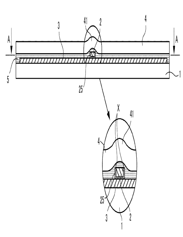
of FIG. 1. As shown in FIGS. 1 and 2, the IC tag according
to the present embodiment includes: a base sheet 1 formed
in a rectangular shape having an upper surface (first
surface) and a lower surface (second surface), an IC chip 2
and an antenna 3 that are arranged on the upper surface of
the base sheet 1, and a protective sheet 4 that is formed
4
CA 03184237 2022 12 23
in a rectangular shape and covers the IC chip 2 and the
antenna 3. Also, the protective sheet 4 is fixed to the
first surface of the base sheet 1 with a bonding agent 5.
Each of these members will be described in detail below.
[0015] Although there is no particular limitation on the
material constituting the base sheet 1, for example, the
base sheet 1 can be made of, for example, polyethylene,
polypropylene, polyvinyl chloride, polyester resins such as
polyethylene terephthalate, polyimide resins, and the like.
Also, the thickness of the base sheet 1 is, for example,
preferably 25 to 200 pm, and more preferably 50 to 150 pm.
[0016] Hereinafter, for convenience of description, as
shown in FIG. 1, sides in the longitudinal direction of the
base sheet 1 and the protective sheet 4 are called a first
side 101 and a second side 102, and sides in a lateral
direction are called a third side 103 and a fourth side
104. Accordingly, these sides are connected in the
following order: the first side 101, the third side 103,
the second side 102, and the fourth side 104.
[0017] The IC chip 2 is a known IC chip having a memory
function, and is electrically connected to a dipole antenna
3 made of a conductor.
[0018] In this embodiment, as an example, a dipole antenna
as shown in FIG. 1 is used. That is, the dipole antenna 3
includes an impedance matching portion 31 arranged near the
center in the longitudinal direction of the base sheet 1,
and a pair of dipole portions 32 extending from the
5
CA 03184237 2022- 12- 23
impedance matching portion 31 in the longitudinal direction
of the base sheet 1. The impedance matching portion 31 is
formed in a rectangular frame shape having first to fourth
sides. More specifically, a first side 311 of the
impedance matching portion 31 is arranged at a position
slightly spaced apart from the first side 101 of the base
sheet 1, and a second side 312 is arranged along the second
side 102 of the base sheet 1. That is, the first side 311,
the third side 313, the second side 312, and the fourth
side 314 of the impedance matching portion 31 are connected
in this order. The IC chip 2 is arranged near the center
of the first side 311 of the impedance matching portion 31.
[0019] Since the dipole portion 32 has a bilaterally
symmetrical shape, only the left side of FIG. 1 will be
described. The dipole portion 32 forms a rectangular frame
so as to extend from the first side 311 of the impedance
matching portion 31 to the first side 101 of the base sheet
1, extend from there along the first side 101, the third
side 103, and the second side 102 of the base sheet 1, and
further extend along the third side 313 of the impedance
matching section 31, and thereafter extends spirally inside
the frame. Note that although there is no particular
limitation on the thickness of the dipole antenna 3, for
example, the thickness can be set to 5 to 20 pm.
[0020] Although there is no particular limitation on the
material constituting the dipole antenna 3, for example,
the dipole antenna 3 can be made of a conductive material
6
CA 03184237 2022- 12- 23
such as silver, copper, or aluminum. When silver is used,
the dipole antenna 3 can be formed by applying a silver
paste containing silver onto the base sheet 1 through
screen printing. On the other hand, when copper or
aluminum is used, the dipole antenna 3 can be formed by
etching, for example. Also, the IC chip 2 is fixed to the
antenna 3 with a conductive bonding agent 25 such as ACP,
for example. In addition, the IC chip 2 can be fixed to
the antenna 3 through known flip-chip mounting for
electronic components. Note that although there is no
particular limitation on the thickness of the IC chip 2,
the thickness can be 100 to 150 pm.
[0021] Information stored in the IC chip 2 can be
transmitted and received by the dipole antenna 3 as
described above, for example, with use of radio waves in
the UHF band.
[0022] The protective sheet 4 is preferably made of a heat-
deformable material, and can be made of the same material
as the base sheet, for example. Also, the thickness of the
protective sheet 4 is, for example, preferably 25 to 250
pm, and more preferably 50 to 150 pm.
[0023] Also, in the protective sheet 4, a protruding
portion 41 protruding along the IC chip 2 is formed at a
location where the IC chip 2 is arranged. More
specifically, the protruding portion 41 is formed above the
IC chip 2 so as to have a roughly arcuate cross section.
Also, in a plan view, the protruding portion 41 is formed
7
CA 03184237 2022- 12- 23
in a substantially circular shape so as to follow the
planar shape of the conductive bonding agent 25. Also, the
IC chip 2 and protective sheet 4 are closest to each other
near the peripheral edge of the IC chip 2. The distance X
of the location where the IC chip 2 and the protective
sheet 4 are closest to each other is, for example,
preferably 1 to 20 pm, more preferably 1 to 12 pm, and
particularly preferably 1 to 8 pm. Also, the lower surface
of the protective sheet 4, that is, the surface facing the
base sheet 1, is lower than the upper surface of the IC
chip 2 in the region outside the protruding portion 41.
[0024] The bonding agent 5 can be made of a material
containing, for example, an acrylic thermosetting resin, an
ester-based thermosetting resin, an epoxy-based
thermosetting resin, or a polyimide-based thermosetting
resin as a main component. Such a thermosetting bonding
agent is suitable for bonding the protective sheet 4 and
the base sheet 1 while forming the protruding portion 41 by
applying pressure, as will be described later. However, a
thermoplastic bonding agent can also be used.
[0025] 2. Manufacturing Method for IC Tag
The IC tag configured as described above can be
formed by various methods, and for example, it can be
formed by the following method. First, as shown in FIG.
3A, the dipole antenna 3 is formed on the base sheet 1 by
an above-described method such as screen printing or
etching. Then, the IC chip 2 is fixed on the dipole
8
CA 03184237 2022- 12- 23
antenna 3 by the above-described method, for example, the
conductive bonding agent 25. Also, a protective sheet 4
having the same size as the base sheet 1 is prepared. The
bonding agent 5 described above is applied to the lower
surface of the protective sheet 4 in advance. Next, as
shown in FIG. 3B, this protective sheet 4 is arranged on
the base sheet 1 so as to cover the dipole antenna 3 and
the IC chip 2.
[0026] Subsequently, as shown in FIG. 30, the base sheet 1
is arranged on the support plate 7, and the support sheet 6
is arranged on the protective sheet 4. This support sheet
6 is an elastically deformable sheet for absorbing
deformation of the protective sheet 4 by the IC chip 2, as
will be described later, and for example, is preferably a
material with a durometer hardness (JIS K7215-1986) of HDD
10 to HDD 90, and more preferably HDD 10 to HDD 70.
Specifically, a resin material such as LDPE (low density
polyethylene), LLDPE (linear low density polyethylene),
HDPE (high density polyethylene), PTFE
(polytetrafluoroethylene resin), EMMA (ethylene-methyl
methacrylate copolymer resin), or EVA (ethylene-vinyl
acetate copolymer resin) can be used. Preferably, the
upper and lower surfaces of the support sheet 6 are coated
with a mold release agent. In addition, as will be
described later, the thickness of the support sheet 6 is
preferably a thickness that can absorb at least the
protruding portion 41 of the protective sheet 4, and for
9
CA 03184237 2022- 12- 23
example, is preferably 50 to 300 pm, and more preferably
100 to 200 pm.
[0027] Then, this support sheet 6 is pressed by a heating
plate 8. The temperature, time, and pressure of the
pressing by the heating plate 8 can be set in various ways,
but the setting needs to be performed such that the IC chip
2 is not damaged by the pressing and the protruding portion
41 is formed on the protective sheet 4 along the IC chip 2.
For example, the temperature is raised from 40 C to 160 C
in about 5 to 30 minutes (more preferably 10 to 20
minutes), and pressing is continued at 160 C for 15 to 50
minutes (more preferably 20 to 40 minutes). Thereafter,
the temperature is lowered from 160 C to 40 C in about 5 to
30 minutes (more preferably 10 to 20 minutes). During this
time, the heating plate 8 presses the support sheet 6 with
a pressure of 1 to 6 MPa, and more preferably 3 to 4 MPa.
Note that although the temperature of the heating plate 8
depends on the materials of the protective sheet 4 and the
support sheet 6, other temperatures may be used. However,
the temperature is preferably a temperature at which the
protective sheet 4 and the support sheet 6 are deformed,
and for example, the starting temperature is preferably 20
to 100 C, and the maximum temperature is preferably 120 to
180 C.
[0028] Also, as shown in FIG. 3D, when the support sheet 6
is pressed by the heating plate 8, the protective sheet 4
is pressed and the bonding agent 5 is also pressed. In
CA 03184237 2022- 12- 23
this process, the location of the protective sheet 4
corresponding to the IC chip 2 is pressed by the IC chip 2
and deforms to protrude upward, forming a protruding
portion 41 having an arcuate cross section. Then, the
protruding portion 41 presses the support sheet 6. That
is, the support sheet 6 plays a role of absorbing the
protruding portion 41 when pressed between the protective
sheet 4 and the heating plate 8. Furthermore, the support
sheet 6 also serves to prevent the IC chip 2 from being
crushed. In this way, after pressing at the time,
pressure, and temperature described above, the heating
plate 8 is separated, and the IC tag as shown in FIGS. 1
and 2 is completed.
[0029] It should be noted that, when pressing the
protective sheet 4 as described above, it is preferable to
use, for example, a vacuum press. This can prevent air
from entering between the bonding agent 5 and the base
sheet 1. In particular, since the IC chip 2 protrudes from
the base sheet 1, air tends to enter the surrounding area
of the IC chip 2. If air enters in this way, the antenna 3
may be disconnected, and therefore it is preferable to use
a vacuum press.
[0030] 3. Features
As described above, according to the present
embodiment, the protective sheet 4 has the protruding
portion 41 formed in a protruding shape along the IC chip
2, and in regions other than the protruding portion 41, the
11
CA 03184237 2022- 12- 23
lower surface of the protective sheet 4 is lower than the
uppermost surface of the IC chip 2 and is close to the base
sheet 1. As a result, the vicinity of the peripheral edge
of the protruding portion 41 and the vicinity of the
peripheral edge of the IC chip 2 are particularly close to
each other, and therefore when the IC tag is folded, for
example, the IC chip 2 is supported by the lower surface of
the protruding portion 41, and therefore it is possible to
prevent the IC chip 2 from being separated from the antenna
3.
[0031] 4. Modified Examples
Although one embodiment of the present invention has
been described above, the present invention is not limited
to the above-described embodiment, and various
modifications are possible without departing from the gist
of the invention. A plurality of modified examples shown
below can be appropriately combined.
[0032] <4-1>
In the above embodiment, the dipole antenna 3 and the
IC chip 2 are sandwiched between the support sheet and the
protective sheet 4. However, for example, as shown in FIG.
4, a sheet-like first cover member 91 and a second cover
member 92 can be further provided respectively on the lower
surface side of the base sheet 1 and the upper surface side
of the protective sheet 4, via a bonding agent 93. Each of
the cover members 91 and 92 can be made of the same
material and with the same thickness as the base sheet 1.
12
CA 03184237 2022- 12- 23
Also, there is no particular limitation on the bonding
agent 93, and the bonding agent 93 may also be a known
double-sided tape. In particular, it is preferable that
the bonding agent 93 between the second cover member 92 and
the protective sheet 4 absorbs the protruding portion 41
and prevents the second cover member 92 from being deformed
by the protruding portion.
[0033] <4-2>
The shape of the dipole antenna 3 described above is
an example, and various shapes are possible. Also, the
position of the IC chip 2 on the antenna 3 is not
particularly limited. Furthermore, various antennas can be
used as the antenna 3, and instead the antenna 3 using the
dipole antenna as described above, an antenna 3 using a
patch antenna may also be used. That is, the shape and the
like of the antenna 3 are not particularly limited, and
various forms are possible.
[0034] <4-3>
The shape of the IC tag, that is, the shape of the
base sheet 1 and the protective sheet 4, is not
particularly limited, and instead of an elongated shape as
described above, various shapes can be used according to
the application, such as a rectangular shape, a circular
shape, or a polygonal shape. Also, the base sheet 1 and
the protective sheet 4 do not necessarily need to have the
same shape, and it is sufficient that the IC chip 2 and the
antenna 3 are arranged at least between the two sheets 1
13
CA 03184237 2022- 12- 23
and 4.
Examples
[0035] Examples of the present invention will be described
below. However, the present invention is not limited to
these examples.
[0036] 1. Preparation of Example and Comparative Example
IC tags according to an example and a comparative
example were prepared as follows. In this example and
comparative example, the base sheet, protective sheet, IC
chip, and antenna are the same, as follows.
[0037] - Base sheet: PET, thickness 100 pm
- Conductive bonding agent: ACP
- IC chip: thickness 120 pm
- Antenna: Printed silver (same shape as Fig. 1),
thickness 10 pm
- Protective sheet with bonding agent: PET, thickness
100 pm, the bonding agent was a thermosetting epoxy resin
with an initial thickness of 50 pm (however, in the
comparative examples, an acrylic pressure-sensitive
adhesive with an initial thickness of 50 pm was used)
[0038] Next, the example was manufactured. At this time,
EMMA with a thickness of 150 pm was used as the support
sheet, and manufacturing was performed as shown in FIGS. 3A
to 3D. Using a vacuum press, the support sheet was pressed
with a heating plate at a pressure of 4 MPa, and the
heating plate was heated from 40 C to 160 C over 20
14
CA 03184237 2022 12 23
minutes. Next, pressing was performed at 160 C for 35
minutes and then cooling was performed to 40 C over 15
minutes. Thus, the IC tag according to the example was
completed. In this example, a protruding portion
protruding in a hemispherical shape was formed on the
protective sheet at a position corresponding to the IC
chip.
[0039] On the other hand, a comparative example was
manufactured as follows. That is, the base sheet and the
protective sheet were bonded to each other by being pressed
by a urethane roller, whereby the IC tag according to the
comparative example was manufactured.
[0040] 2. Evaluation Test
Next, a bending test was performed on the example and
the comparative example. That is, as shown in FIG. 5A, the
IC tag was folded approximately in half with the IC chip at
the center so that both sides face upward, and then, as
shown in FIG. 5B, the IC tag was folded approximately in
half with the IC chip at the center so that both sides face
downward. After performing this for 20 cycles, it was
checked whether or not the IC chip separated. As a result,
the IC chip did not separate from the antenna in the
example, but the IC chip separated from the antenna in the
comparative example.
LIST OF REFERENCE NUMERALS
[0041] 1 Base sheet
CA 03184237 2022- 12- 23
2 IC chip
3 Antenna
4 Protective sheet
Bonding agent
5
16
CA 03184237 2022- 12- 23