Note: Descriptions are shown in the official language in which they were submitted.
CA 03186265 2022-12-05
WO 2021/245372 PCT/GB2021/051273
- 1 -
RECONFIGURABLE ARRAY FOR RF/ANALOGUE SIGNALS
FIELD OF THE INVENTION
The present invention relates to a reconfigurable array for facilitating
dynamic
combination and distribution of RF/analogue signals.
BACKGROUND OF THE INVENTION
Light can be modulated by a data-carrying radio frequency signal and
transmitted
over an optical fibre link. This is referred to as RF over fibre (or radio
over fibre). There are
many communications applications of RF over fibre, including transmission of
mobile radio
signals (3G, 4G, 5G and WiFi) and cable television signals. RF over fibre is
also used in
satellite base station communications. Fibre optic links are advantageous
because they
provide lower transmission losses and reduced sensitivity to noise and
electromagnetic
interference compared to all-electrical signal transmission. Thus, RF over
fibre can be used
to transport analogue RF signals of very high bandwidth over long distances
with very low
loss and electromagnetic isolation from the environment. The present
application aims to
provide a versatile solution in terms of distribution of RF signals which
provides various
advantages over those of the prior art.
SUMMARY OF THE INVENTION
According to the present invention, there is provided a reconfigurable array
for
facilitating dynamic combination and distribution of RF/analogue signals. The
reconfigurable
array comprises: a number (N,) of input devices for generating or supplying
RF/analogue
input signals; a number (No) of output devices for analysing or forwarding
RF/analogue
output signals; an optical switch matrix comprising a number (No) of ports;
and a plurality of
splitters/combiners that each have multiple uncommon ports which couple to a
single
common port. Each of the ports of the optical switch matrix is an optical
input or an optical
output. Each input device is coupled to a respective port of the optical
switch matrix at an
optical input, and each output device is coupled to a respective port of the
optical switch
matrix at an optical output. The optical switch matrix is configurable to
enable optical
connection of any optical input to any optical output. Each splitter/combiner
enables either
fan-in of optical signals from the uncommon ports to the common port or fan-
out of optical
signals from the common port to the uncommon ports. Each port of each
splitter/combiner
is coupled to a respective port of the optical switch matrix. The plurality of
CA 03186265 2022-12-05
WO 2021/245372 PCT/GB2021/051273
- 2 -
splitters/combiners include at least one M:1 splitter/combiner, where M is a
predetermined
maximum number of RF/analogue signals for the reconfigurable array to fan-in
or fan-out,
where N, and N,.
An alternative for achieving fan-out uses a tuneable optical filter
architecture.
However, such an arrangement band limits very wideband RF signals and
generally has a
deleterious effect on linearity. In contrast, the present reconfigurable array
has no
bandwidth limiting optical features.
An alternative for achieving fan-in is described below in relation to Figure
1.
However, as will be discussed below, this solution is not scalable. In
contrast, the present
reconfigurable array is completely scalable and may be designed to enable
unconstrained
fan-in/fan-out for all input and output devices, or may be constrained to
limit the fan-in/fan-
out options by means of the number M.
The input devices may include one or more of: a receiving antenna; a software
defined radio, SDR, transmitter; and an RF/analogue signal generator.
The output devices include one or more of: a transmitting antenna; an SDR
receiver;
and an RF/analogue signal analyser.
Each input device may be coupled to the respective port of the optical switch
matrix
by means of a respective electrical-to-optical (E/O) converter configured to
convert the
respective RF/analogue signal into a corresponding optical signal for
distribution through
the optical switch matrix. The E/O converters for each of the input devices
may be
configured to generate optical signals having different optical wavelengths to
one another.
Each output device may be coupled to the respective port of the optical switch
matrix by means of a respective optical-to-electrical (0/E) converter
configured to convert
an optical signal received from the optical switch matrix into an RF/analogue
signal for
analysis or onward transmission by the output device. Each 0/E converter may
be
configured to provide automatic gain control by controlling a respective
RF/analogue
amplifier based on a measured light level of the received optical signal so as
to adjust an
output power of the respective RF/analogue signal to a predetermined level.
The plurality of splitters/combiners may include duplicate splitters/combiners
to
provide redundancy in case of failure of one or more of the plurality of
splitters/combiners.
In a first embodiment, the optical switch matrix is an any-to-any optical
switch
matrix, where each of the ports is reconfigurable as either an optical input
or an optical
CA 03186265 2022-12-05
WO 2021/245372 PCT/GB2021/051273
- 3 -
output, and where the any-to-any optical switch matrix is configurable to
enable optical
connection of any one of the ports to any other one of the ports.
In the first embodiment, the plurality of splitters/combiners may be defined
as
follows: (a) A is defined as max(N,, No) and B is defined as min(Nõ No), (b)
for 1= 1, 2, ...,
the 1th splitter/combiner is an X,:1 splitter/combiner, where X,= A/i rounded
down to the
nearest integer, (c) if X, < 2, the 1th splitter/combiner is excluded from the
plurality of
splitters/combiners and the number of splitters/combiners in the plurality of
splitters/combiners is defined as S, and (d) the total number of ports is
given by
p = N1+ N0+ 1(X1+1).E.7_
In one example of the first embodiment, M= A such that the reconfigurable
array is
unconstrained to enable fan-in from all of the input devices or fan-out to all
of the output
devices if desired. Alternatively, M <A such that the reconfigurable array is
constrained to
enable fan-in from a maximum of M input devices or fan-out to a maximum of M
output
devices, wherein each X, is constrained by X, M.
In a second embodiment, the optical switch matrix is a CxD optical switch
matrix
having a number (C) of ports on one side and a number (D) of ports on the
other side,
where C D, and where the CxD optical switch matrix 630 is configurable to
enable optical
connection of any of the C ports on the one side to any of the D ports on the
other side. In
the second embodiment, the plurality of splitter/combiners comprises a first
set of
splitters/combiners having their uncommon ports connected to respective ones
of the D
ports of the optical switch matrix and having their common ports connected to
respective
ones of the C ports of the optical switch matrix. In the second embodiment,
the plurality of
splitter/combiners comprises a second set of splitters/combiners having their
uncommon
ports connected to respective ones of the C ports of the optical switch matrix
and having
their common ports connected to respective ones of the D ports of the optical
switch matrix.
In one example of the second embodiment, N1> No such that each input device is
coupled to a respective one of the C ports of the optical switch matrix, and
each output
device is coupled to a respective one of the D ports of the optical switch
matrix.
Alternatively, N, < No such that each input device is coupled to a respective
one of the D
ports of the optical switch matrix, and each output device is coupled to a
respective one of
the C ports of the optical switch matrix.
In the second embodiment, the first set of splitters/combiners may be defined
as
follows: (a) A is defined as max(N,, No) and B is defined as min(Nõ No); (b)
for i= 1, 2, ...,
CA 03186265 2022-12-05
WO 2021/245372 PCT/GB2021/051273
- 4 -
the 1th splitter/combiner in the first set of splitters/combiners is an X,:1
splitter/combiner,
where X, = Ali rounded down to the nearest integer; and (c) if X, < 2, the it"
splitter/combiner
is excluded from the first set of splitters/combiners and the number of
splitters/combiners in
the first set of splitters/combiners is S. If desired, each X, may be
constrained by X, P,
where P is a predetermined maximum number of RF/analogue signals for the first
set of
splitters/combiners to fan-in or fan-out, where A.
In the second embodiment, the second set of splitters/combiners may be defined
as
follows: (a) for i= 1, 2, ..., the it" splitter/combiner in the second set of
splitters/combiners is
an Y,:1 splitter/combiner, where Y= Bli rounded down to the nearest integer;
and (b) if Y,<
2, the it" splitter/combiner is excluded from the second set of
splitters/combiners and the
number of splitters/combiners in the second set of splitters/combiners is T If
desired, each
Y, may be constrained by Y, 0, where Q is a predetermined maximum number of
RF/analogue signals for the second set of splitters/combiners to fan-in or fan-
out, where
<B.
In the second embodiment, the numbers C and D of ports required may be given
by:
C= A + S Yi and D= B + T + E.7_1 X
Other preferred features of the present invention are set out in the appended
claims.
BRIEF DESCRIPTION OF THE DRAWINGS
Embodiments of the present invention will now be described by way of example
with
reference to the accompanying drawings in which:
Figure 1 schematically illustrates an exemplary system for routing RF over
fibre
signals;
Figure 2a schematically illustrates a reconfigurable array for facilitating
dynamic
combination and distribution of RF/analogue signals between four input devices
and six
output devices;
Figure 2b schematically illustrates a specific example of the reconfigurable
array of
Figure 2a where the input devices are antennas and the output devices are
Software
Defined Radios (SDRs);
Figure 3 schematically illustrates a reconfigurable array according to a first
embodiment of the present invention including an any-to-any optical switch
matrix for
routing/distributing optical signals between six input devices and four output
devices;
CA 03186265 2022-12-05
WO 2021/245372 PCT/GB2021/051273
- 5 -
Figure 4 schematically illustrates an exemplary configuration of the
reconfigurable
array of Figure 3;
Figure 5 schematically illustrates another exemplary configuration of the
reconfigurable array of Figure 3; and
Figure 6 schematically illustrates a reconfigurable array according to a
second
embodiment of the present invention including a CxD optical switch matrix for
routing/distributing optical signals between six input devices and four output
devices.
DETAILED DESCRIPTION OF A PREFERRED EMBODIMENT
For applications that require more than just point-to-point connections, where
fan-in
(combining) or fan-out (splitting) distribution is desired, optical solutions
can support these
requirements. In particular, RF over fibre can be used to multiplex many
channels on a
single fibre for high density, small footprint distribution using wavelength
division
multiplexing (WDM).
A known system 100 for routing RF over fibre signals is shown in Figure 1. RF
over
fibre refers to analogue over fibre, as opposed to digital over fibre. As
mentioned in the
Background section, the analogue (e.g. RF) data signal is used to modulate an
optical (e.g.
laser) carrier signal. In many applications, the analogue data signal is a
radio frequency
signal (hence the terminology `RF over fibre'), but a lower frequency analogue
data signal
(e.g. a 20Hz audio signal) or a DC data signal (having high and low states)
could also be
used to modulate the optical carrier signal. Thus, in this application, the
term `RF over fibre'
encompasses an analogue data signal (DC up to 300GHz) being modulated onto an
optical
carrier signal and transmitted via an optic fibre; the data signals are
described herein as
RF/analogue signals. Figure 1 shows four RF over fibre inputs 110a-d on the
left hand side,
each of which provides an input signal having a different wavelength (A-D).
Each of these
four RF over fibre input signals is split by a respective splitter 120a-d into
four separate
signals. The system 100 further includes four switch arrays 130a-d. Each
switch array 130
feeds into a respective combiner 140a-d. Each combiner 140 is associated with
a
respective RF over fibre output 150a-d.
The four signals output by each splitter 120 are fed into four switches, one
from
each of the four switch arrays 130. For example, the split signals output by
the first splitter
120a feed into (a) a first switch of the first switch array 130a, (b) a first
switch of the second
switch array 130b, (c) a first switch of the third switch array 130c, and (d)
a first switch from
the fourth switch array 130d. Thus, each switch array 130 receives one input
signal from
CA 03186265 2022-12-05
WO 2021/245372 PCT/GB2021/051273
- 6 -
each of the four splitters 120. In other words, each of the receivers receives
a version of
each input signal, regardless of the fact that they may only be interested in
a single input
signal. Depending on which input signals are selected using the switches of
the switch
arrays 130, the combiners 140 each act to combine the selected input signals
to provide an
output signal to the respective output 150. Thus, each switch array 130 and
associated
combiner 140 may be considered as a tunable filtering element. For example,
the first
switch array 130a may be used to select the first input signal only such that
the output from
the first combiner 140a is based on the first input signal only. The second
switch array 130b
may be used to select the second and third input signals only such that the
output from the
second combiner 140b is based on a combination of the second and third input
signals. The
third switch array 130c may be used to select the first and third input
signals only such that
the output from the third combiner 140c is based on a combination of the first
and third
input signals. The fourth switch array 130d may be used to select all of the
input signals
such that the output from the fourth combiner 140b is based on a combination
of all of the
input signals.
Using the known system of Figure 1, any input 110 can be routed to any output
150,
with signal combination as necessary. However, if more than four inputs are
required, the
required number of components and the complexity of the system both increase
substantially. Furthermore, as the number of inputs increases from the four
shown in Figure
1 to an arbitrary large number N, it will be appreciated that the splitting
losses also increase
since each input signal is split into N separate signals, with a consequent
reduction in
amplitude. In this case, optical amplification is likely to be required, which
adds significant
complexity in terms of the implementation. Furthermore, the architecture of
Figure 1 is
unidirectional. Therefore, the system of Figure 1 is in many ways not
practical when
considering a larger number of inputs and outputs. Nonetheless, from this
starting point, it is
desired to design a completely reconfigurable signal distribution/routing
array where
numerous input devices require reconfigurable access to multiple output
devices, without
the disadvantages described with reference to Figure 1.
6x4 Reconfiqurable Array Using Any-To-Any Optical Switch Matrix
A signal distribution/routing array where numerous input devices require
reconfigurable access to multiple output devices is schematically illustrated
in Figure 2a.
The example of Figure 2a includes four input devices 210 and six output
devices 220 with a
reconfigurable distribution/routing arrangement 230 between them. Equally, the
system of
CA 03186265 2022-12-05
WO 2021/245372 PCT/GB2021/051273
- 7 -
Figure 2a could be used in reverse such that there are six input devices and
four output
devices. Of course, it will be appreciated that any number of input and output
devices may
be present depending on the desired use case. In general, the input devices
generate or
supply RF/analogue signals, so could be RF/analogue source devices such as
receiving
antennas, SDR transmitters (TX), or other RF/analogue signal generators. The
output
devices analyse or forward RF/analogue signals, so could be RF/analogue sink
devices
such as transmitting antennas, SDR receivers (RX), or other RF/analogue signal
analysers
(e.g. test devices).
As a specific example, Figure 2b shows the input and output devices as six
antennas 250 and four SDRs 260. Each antenna 250 in Figure 2 can be either an
input
device 210 (i.e. a receiving antenna) or an output device 220 (i.e. a
transmitting antenna).
In addition, each SDR 260 in Figure 2 can be either an input device 210 (i.e.
an SDR TX
which generates RF/analogue signals) or an output device 220 (i.e. an SDR RX
which
analyses RF/analogue signals). Furthermore, single or many connections to an
SDR 260 or
antenna 250 may be necessary to meet the following requirements:
(a) One SDR TX connected to many antennas is required in the case of a
distributed
antenna which is able to transmit in multiple directions. Equally, this
arrangement is
useful where high frequency directionality of transmission is required. In
this
example, the SDR TX in an input device 210, and the antennas are output
devices
220.
(b) Many SDR TX connected to one antenna is required for broadband composite
signal generation. In this example, the SDR TXs are input devices 210, and the
antenna is an output device 220.
(c) One antenna connected to many SDR RX is required for multi-carrier high
throughput demodulation. In this example, the antenna is an input device 210,
and
the SDRs are output devices 220.
(d) Many antenna connected to one SDR RX is useful at low frequencies for
efficient
SDR usage. In this example, the antennas are input devices 210, and the SDRs
are
output devices 220.
(e) Antenna to antenna connections are used in repeater stations.
(f) SDR TX to SDR RX connections may be required to use the optics as radio-to-
radio
over long distance fibres.
CA 03186265 2022-12-05
WO 2021/245372 PCT/GB2021/051273
- 8 -
Thus, a bidirectional, reconfigurable signal distribution/routing arrangement
230 between
the input devices 210 and the output devices 220 is desirable, including
options for fan-in
and fan-out. Such an arrangement could be used to re-purpose communications
infrastructure (e.g. antennas) to inject electronic countermeasure waveforms
to block
certain communications. This can be done using fan-in functionality to combine
the signal-
to-be-blocked with an opposing signal which can jam or obliterate the signal-
to-be-blocked.
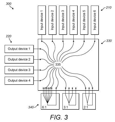
Accordingly, a suitable reconfigurable array 300 for facilitating dynamic
combination
and distribution of RF/analogue signals is schematically illustrated in Figure
3. The
reconfigurable array 300 comprises input devices 210 for generating or
supplying
RF/analogue signals, output devices 220 for analysing or forwarding
RF/analogue signals,
an optical switch matrix 330, and a plurality of splitters/combiners 340 to
enable fan-in or
fan-out of optical signals. In the exemplary arrangement of Figure 3, there
are six input
devices 210 and four output devices 220, but it will be understood that any
number of input
and output devices could be used depending on the use case.
The optical switch matrix 330 comprises a number of ports 335, the number
designated N. Note that most, but not all of the ports 335 are labelled in
Figure 3. In the
arrangement of Figure 3 there are 24 ports 335 (i.e. Np = 24), but it will be
appreciated that
this is exemplary such that a different number of ports 335 may be provided
depending on
the implementation requirements in a particular case. In the example of Figure
3, the optical
switch matrix 330 is a so-called "any-to-any" optical switch matrix that is
fully configurable to
enable optical connection of any one of the ports 335 to any other one of the
ports 335.
Each of the ports 335 acts as an optical input to or an optical output from
the optical switch
matrix 330. Furthermore, each of the ports 335 of the any-to-any optical
switch matrix 330
is reconfigurable from being an optical input to an optical output (or vice
versa), and may
switch seamlessly between the two. Thus, the optical switch matrix 330 is
reconfigurable,
fully bidirectional, and has low loss and high isolation. The optical switch
matrix 330 is also
non-blocking in that no optical connections block other optical connections
therethrough. An
exemplary any-to-any optical switch matrix with 48 ports is the Polatis Series
6000 48xCC
OSM available from Huber+Suhner (see hgps://www,pdatis.cornisvvitch- modules-
tor-oe
switch-module-solutions- orioinal-eauipment- ma nufacturesaso).
The number of input devices 210 is designated N,. In the arrangement of Figure
3
there are six input devices 210 (i.e. Ni= 6), but it will be appreciated that
this is exemplary
such that a different number of input devices 210 may be provided. Each input
device 210
is coupled to a respective port 335 of the optical switch matrix 330 at an
optical input.
CA 03186265 2022-12-05
WO 2021/245372
PCT/GB2021/051273
- 9 -
The number of output devices 220 is designated No. In the arrangement of
Figure 3
there are four output devices 220 (i.e. No = 4), but it will be appreciated
that this is
exemplary such that a different number of output devices may be provided. Each
output
device 220 is coupled to a respective port 335 of the optical switch matrix
330 at an optical
output.
The splitters/combiners 340 are used to address requirements (a)-(f) listed
above.
The splitters/combiners 340 are reconfigurable and bidirectional. Thus, each
splitter/combiner 340 has multiple uncommon ports which couple to a single
common port.
Each splitter/combiner 340 enables either fan-in of optical signals from the
uncommon ports
to the common port, or fan-out of optical signals from the common port to the
uncommon
ports, depending on the direction in which the splitter/combiner 340 is
connected. in
particular, when connected in one direction, a splitter/combiner 340 acts as a
combiner
where inputs to the uncommon ports are fanned-in to the common port (i.e.
there is a
many-to-one configuration of splitter/combiner inputs to splitter/combiner
outputs). When
connected in the opposite direction, a splitter/combiner 340 acts as a
splitter where an input
to the common port is fanned-out to the uncommon ports (i.e. there is a one-to-
many
configuration of splitter/combiner inputs to splitter/combiner outputs). Each
port
(common/uncommon) of each splitter/combiner 340 is coupled to a respective
port 335 of
the optical switch matrix 330. The plurality of splitters/combiners include at
least one M:1
splitter/combiner, where M is a predetermined maximum number of RF/analogue
signals for
the reconfigurable array to fan-in or fan-out, where N,
and No. In the example of
Figure 3, M= 6. Thus, the 6:1 splitter/combiner may be used to fan-in all of
the signals from
the six input devices 210. Equally, the 6:1 splitter/combiner may be used to
fan-out a single
input signal to all of the four output devices 220. The plurality of
splitters/combiners 340 in
the reconfigurable array 300 of Figure 3 further include a 3:1
splitter/combiner and a 2:1
splitter/combiner 340.
Notably, each port 335 of the optical switch matrix 330 is configured to
connect to a
single optical input or output. Thus, if an optical switch matrix port 335 is
coupled to an input
device 210, it cannot also be coupled to an output device 220 or to a
common/uncommon
port of a splitter/combiner 340 or even to another input device 210.
Regarding inputs into the optical switch matrix 330, each input signal should
be an
optical input signal. Thus, an RF/analogue input signal from an input device
210 is
converted to an optical signal prior to its presentation at a port 335 of the
optical switch
matrix 330. Equally, outputs from the optical switch matrix 330 will all be
optical output
CA 03186265 2022-12-05
WO 2021/245372 PCT/GB2021/051273
- 10 -
signals. Thus, it is also necessary to convert such output signals back to
RF/analogue for
onward transmission or processing by the output devices 220. For this reason,
each input
device 210 may be coupled to its respective port 335 of the optical switch
matrix 330 by
means of a respective electrical-to-optical (E/O) converter (not shown). Each
E/O converter
is configured to convert an incoming RF/analogue signal into a corresponding
optical signal
for distribution/routing through the optical switch matrix 330. As is known,
this may be
achieved by modulating a light source intensity with the RF/analogue signal to
generate a
corresponding optical signal. In addition, each output device is coupled to
the respective
port of the optical switch matrix 330 by means of a respective optical-to-
electrical (0/E)
converter (not shown). Each 0/E converter is configured to convert an optical
signal from
the optical switch matrix 330 into an RF/analogue signal for analysis or
onward
transmission by the relevant output device 220. As is also known, this may be
achieved by
demodulation of the optical signal. If an input device 210 or output device
220 is remote
from the optical switch matrix 330, an optical fibre (of up to several
kilometres in length)
may extend between the relevant E/O or 0/E converter and the associated port
335 of the
optical switch matrix 330.
When generating optical inputs into the optical switch matrix 330, it is
important that
any optical inputs destined to be combined by one of the splitters/combiners
340 have
different wavelengths assigned to enable wavelength-division multiplexing
(WDM). This can
be achieved if the E/O converters for each of the input devices 210 are
configured to
generate optical signals having different optical wavelengths (or wavelength
bands) to one
another. Of course, if signals from one or more of the input devices 210 are
never required
to be combined with signals from any of the other input devices 210, it will
be understood
that those input devices 210 need not have distinct wavelengths (or wavelength
bands)
associated with them. Note that the use of an optical switch matrix 330
enables fan-in of
signals in a highly linear manner for frequency stacking each of the generated
optical
signals, and this is clearly advantageous.
Each of the 0/E converters includes an optical receiver configured to receive
an
optical signal from the optical switch matrix 330 for subsequent conversion
into an
RF/analogue signal for onward transmission to the relevant output device 220.
Notably,
optical receivers are by their nature wideband and will respond to any
wavelengths present.
In cases where optical signals are split by one or more of the
splitters/combiners
340 as they pass through the optical switch matrix 330, there will be a
consequent
reduction in amplitude of the optical signal. In addition, the optical loss of
the
CA 03186265 2022-12-05
WO 2021/245372 PCT/GB2021/051273
-11 -
splitters/combiners 340 can be different (e.g. there will generally be a
greater optical loss
when using a 6:1 splitter/combiner as compared to using a 2:1
splitter/combiner). Thus, the
0/E converters may also be configured to provide automatic gain control to
compensate for
this. In this case, each 0/E converter includes a respective RF/analogue
amplifier, and the
automatic gain control may be achieved by controlling the RF/analogue
amplifier based on
a measured light level of the received optical signal so as to adjust an
RF/analogue output
power to a predetermined level. In this way, the different optical paths can
be gain balanced
if deemed necessary.
Figure 3 shows the optimal unconstrained arrangement of splitters/combiners
340
for the 6x4 example (which has six input devices 210 and four output devices
220). With
this arrangement, all requirements can be met without restriction/constraint
on fan-in or fan-
out. In other words, the unconstrained example of Figure 3 enables fan-in of
all six input
devices 210 or fan-in of any subgroups of input devices 210. Similarly, the
unconstrained
example of Figure 3 enables fan-out to all four output devices 220 or fan-out
to any
subgroups of output devices 220. The full configuration options are set out in
Table 1
below:
No. of input devices: 6
No. of output devices: 4
Unconstrained (i.e. M = 6)
Total no. of SIC ports: 14
Total no. of parts: 24
SifC: 6:1 3:1 21 Direct output connections
No. of SIC uncommon ports: 6 3 2 connections to
common
Total no. of SIC ports: 7 4 3 VC ports
A 6
1
4 2
4 1 1
3 3
3 2 1
3 1 1 1
2 2 2
12 2 1 1
1 2 1 1 1
Table 1
CA 03186265 2022-12-05
WO 2021/245372 PCT/GB2021/051273
- 12 -
In Table 1, S/C is shorthand for "splitter/combiner". The number of uncommon
ports
for each splitter/combiner 340 is shown, as well as the total number of
optical switch matrix
ports 335 that are required for each splitter/combiner 340. In each case, the
number of
optical switch matrix ports 335 required for each splitter/combiner 340 is
equal to the
number of uncommon ports plus one (for the common port). This is clearly
depicted for the
splitters/combiners 340 in Figure 3 (e.g. the 6:1 splitter/combiner 340 is
connected to 7
ports 335 of the optical switch matrix 330). Note that, for each
configuration, there are only
entries in four columns at most, since, in this example, there are only four
output devices
220 to which the input devices may ultimately be connected.
Configurations A-J in Table 1 depict all possible required configurations for
fan-in of
the six input devices 210. For example, configuration A involves all six input
devices 210
being connected to a single output device 220 by means of the 6:1
splitter/combiner 340. If
the input devices 210 were antennas and the single output device 220 was an
SDR, this
arrangement could be used for requirement (d) listed above. If the input
devices 210 were
SDRs and the single output device 220 was an antenna, this arrangement could
be used
for requirement (b) listed above. It is clear that any one-to-one mapping of
any input device
210 to any output device 220 is possible, bypassing all splitters/combiners
340. This is used
to some extent in all of configurations B, D, F, G, I and J. For example,
configuration D
connects four of the input devices 210 to one output device 220 by means of
the 6:1
splitter/combiner 340, with the other two input devices 210 being directly
connected to
respective output devices 220 without the need for splitting/combining.
Configuration E
involves connecting three input devices 210 to one output device 220 by means
of the 6:1
splitter/combiner 340, and connecting the other three input devices 210 to
another output
device 220 by means of the 3:1 splitter/combiner 340. The 2:1
splitter/combiner 340 is only
required for configuration H where the input ports 335 are separated into
three pairs.
Nonetheless, it will be appreciated that the 2:1 splitter/combiner 340 could
be used instead
of the 3:1 splitter/combiner 340 in configurations C, F, I and J. Equally, the
3:1
splitter/combiner 340 could be used instead of the 6:1 splitter/combiner 340
in
configurations F, G and I. This may be desirable to reduce splitting losses.
Notably, one of
the input devices 210 is not used in configuration J, so this is an unlikely
scenario in the 6x4
example.
An example of the configurability of the reconfigurable array 300 to meet the
different distribution requirements is shown in Figure 4. In this example, the
3:1
splitter/combiner is not used. Input device 1 is directly connected to output
device 1 without
CA 03186265 2022-12-05
WO 2021/245372 PCT/GB2021/051273
- 13 -
passing through a splitter/combiner. In addition, input devices 2, 3, 5 and 6
are all
connected to uncommon ports of the 6:1 splitter/combiner for onward connection
to output
device 4. Also, input device 4 is connected to the common port of the 2:1
splitter/combiner
for onward connection to output devices 2 and 3. This corresponds to
configuration D in
Table 1. Importantly, if the distribution requirements change, then the
optical switch matrix
330 may be reconfigured to provide different connections as desired.
A further example of the configurability of the reconfigurable array 300 to
meet the
different distribution requirements is shown in Figure 5. In this example,
input devices 3, 4,
5, and 6 are connected to four of the six uncommon ports of the 6:1
splitter/combiner so as
to combine the four signals. The common ports of the 6:1 and 2:1
splitters/combiners are
then connected such that the combined signal is split into two to provide
output signals to
output devices 1 and 2. Again, the 3:1 splitter/combiner is not used in this
example.
Whilst a 6x4 example of the reconfigurable array 300 is described above, it
will be
understood that the reconfigurable array 300 may be expanded to account for
larger
distribution requirements. As the size of the system increases (in terms of
the numbers Nõ
N, of input and output devices 210, 220), it may not be feasible to support an
unconstrained
system due to the number of splitters/combiners 340 required, and the
consequent size of
the optical switch matrix 330. Constraining the array in terms of fan-in/fan-
out requirements
can significantly reduce the optical switch matrix size (i.e. Np) by altering
or dropping some
of the splitter/combiner options. Furthermore, a typical deployment will not
generally require
unconstrained flexibility as not all input and output devices 210, 220 will be
the same and
there is often a known set of input and output devices 210, 220 that require
support for fan-
in/fan-out, and this can be designed into the reconfigurable array 300.
An example of a constrained 6x4 reconfigurable array 300 is shown in Table 2
where the predetermined maximum number of RF/analogue signals for the
reconfigurable
array to fan-in or fan-out is M= 4. As can be seen, this means that a 4:1
splitter/combiner
may be used in place of the 6:1 splitter/combiner 340 of Figure 3, which
reduces the total
number Np of required ports 335 from 24 to 22. This is a relatively small
saving in terms of
the number Np of ports 335, but the savings can be very significant when
constraining a
larger reconfigurable array 300.
CA 03186265 2022-12-05
WO 2021/245372
PCT/GB2021/051273
- 14 -
No. of input devices: 6
No. of output devices: 4
Constrained (M = 4)
Total no. of SIC ports: 12
Total no. of parts: 22
SIC: 4:1 3:1 2:1 Direct output connections
No. of SIC uncommon ports: 4 3 2 connections to
common
Total no. of 51C ports: S 4 3 SiC ports
A 4
4 1 1
3 2 1
3 1 11
2 2 1 1
2 1 1
Table 2
The described reconfigurable array 300 could be used in many communications
applications, such as the distribution requirements (a)-(f) listed above.
Generalised Reconfiqurable Array Using Any-To-Any Optical Switch Matrix
For a general Nix N, unconstrained reconfigurable array 300, it is possible to
calculate the splitter/combiner requirements as follows:
= Define A = max(Nõ N0)
= Define B = min(Nõ N0)
= For i= 1,2, ..., the 1th splitter/combiner is an X,:1 splitter/combiner,
where Xi = Ali
rounded down to the nearest integer
= Note that if X,< 2, the it" splitter/combiner is not required and should be
omitted,
such that the full set of splitters/combiners has already been determined,
with the
total number of splitters/combiners being designated S.
The total number of ports required is given by:
= + No +(X1+ 1)
i=1
CA 03186265 2022-12-05
WO 2021/245372 PCT/GB2021/051273
- 15 -
Then, consider constraining the N, x No reconfigurable array 300 such that
there is a
predetermined maximum number (M) of RF/analogue signals for the reconfigurable
array to
fan-in or fan-out. In this case, the unconstrained splitter/combiner
requirements (as
calculated above) should be modified as follows:
= Constrain each X, as follows: X, M
In each case (constrained/unconstrained), note that the system is symmetric.
In
other words, the same splitter/combiner requirements and the same number of
optical
switch matrix ports occur regardless of whether you have, e.g., 10 input
devices and 72
output devices, or 72 input devices and 10 output devices.
Consider an exemplary reconfigurable array 300 having N, = 16 and No = 6 (i.e.
A =
16 and B = 6). In this case, the splitters/combiners 340 required to provide
an
unconstrained system (M= 16) would be as follows: 16:1, 8:1, 5:1, 4:1, 3:1,
2:1. Thus, the
total number Np of ports 335 required for the optical switch matrix 330 would
be 66. If the
16x6 (or 6x16) reconfigurable array 300 were constrained such that the
predetermined
maximum number of RF/analogue signals for the reconfigurable array to fan-in
or fan-out is
M= 6, the splitters/combiners 340 required would be as follows: 6:1, 6:1, 5:1,
4:1, 3:1, 2:1.
This reduces the total number Np of required ports to 54.
As another example, consider a reconfigurable array 300 having N, = 32 and No
= 6
(i.e. A = 32 and B= 6). In this case, the splitters/combiners 340 required to
provide an
unconstrained system (M= 16) would be as follows: 32:1, 16:1, 10:1, 8:1, 6:1,
5:1. Thus,
the total number Np of ports 335 required for the optical switch matrix 330
would be 121. If
the 32x6 reconfigurable array 300 were constrained to M= 8, the
splitters/combiners 340
required would be as follows: 8:1, 8:1, 8:1, 8:1, 6:1, 5:1. this reduces the
total number Np of
required ports 335 to 87. If the 32x6 reconfigurable array 300 were further
constrained to M
= 6, the splitters/combiners 340 required would be as follows: 6:1, 6:1, 6:1,
6:1, 6:1, 5:1.
This further reduces the total number Np of required ports 335 to 79.
The M-constrained system described above is just one example of the sort of
constraint that may be applied to the reconfigurable array 300 when deciding
which
splitter/combiners 340 should be included. Other types of constraint are
possible to meet
system requirements. For example, a 16x6 system could be constrained to
provide fan-in
for up to 8 input devices 210, with the remaining input devices 210 only
requiring a
CA 03186265 2022-12-05
WO 2021/245372 PCT/GB2021/051273
- 16 -
maximum of 4 to be fanned-in. This would require the following
splitters/combiners: 8:1, 4:1,
4:1, 4:1, 3:1, 2:1. Thus, it will be appreciated that the system is fully
configurable to provide
any required signal routing/distribution requirements with the minimum number
of optical
components and optical ports. Given size, weight and power constraints, an
array of optical
components can be added to the optical switch matrix 330 to provide the
functionality
required.
Any-to-any optical switch matrices are available to buy with a number of ports
that is
a multiple of 16 (i.e. Np = 16n, where n is an integer). This is because the
switches tend to
be built in slices of 16 ports per slice. Thus, in cases where the constrained
or
unconstrained system has spare optical ports 335, additional
splitters/combiners 340 may
be included for redundancy purposes in order to cope with any component
failures or to
maximise availability. For example, in the unconstrained 6x4 example of Figure
3, if it were
not possible to obtain a 24-port optical switch matrix 330, then a 2-slice, 32-
port optical
switch matrix 330 could be used, leaving 8 spare ports. These could be used to
provide an
additional (redundant) 6:1 splitter/combiner, or additional (redundant) 3:1
and 2:1
splitters/combiners, as desired. An important aspect of constraining the
signal
routing/distribution requirements is to reduce the number of ports required
since costs go
up considerably with each additional slice added to the optical switch matrix.
6x4 Reconficiurable Array Using CxD Optical Switch Matrix
Whilst the optical switch matrix described above was an any-to-any optical
switch
matrix 330, this is not an essential feature. Alternative embodiments are
envisaged using a
CxD optical switch matrix 630, as described below with reference to Figure 6.
A CxD
optical switch matrix comprises a number (C) of ports on one side and a number
(D) of
ports on the other side, where we will assume C D. CxD optical switch matrix
matrices are
bidirectional, so that a CxD optical switch matrix may be operated with the C
ports as input
ports and the D ports as output ports, or the other way around with the C
ports as output
ports and the D ports as input ports. A CxD optical switch matrix 630 is
configurable to
enable optical connection of any of the C ports on the one side to any of the
D ports on the
other side. Thus, any optical input may be connected to any optical output.
Such optical
switch matrices allow simultaneous connection between optical inputs and
outputs in a fully
non-blocking, all-optical, cross-connect configuration. Exemplary CxD optical
switch
matrices are the MEMS Matrix Optical Switches available from DiCon
Fiberoptics, Inc. (see
h tos://www,diconfiberoptics.comiproductsimems matrix opticai switches.pta2).
Features
CA 03186265 2022-12-05
WO 2021/245372 PCT/GB2021/051273
- 17 -
of the CxD optical switch matrix embodiment described below should be
considered to be
similar to those of the any-to-any optical switch matrix embodiments described
above,
except where described differently below.
The reconfigurable array 600 of Figure 6 comprises input devices 210, output
devices 220, a CxD optical switch matrix 630, and a plurality of
splitters/combiners 640 to
enable fan-in or fan-out of optical signals. To enable a direct comparison to
Figure 3, there
are six input devices 210 (i.e. N, = 6) and four output devices 220 (i.e. No =
4) shown in
Figure 6. In particular, Figure 6 shows the same 6x4 connection configuration
as is shown
in Figure 4, but using the CxD optical switch matrix 630 rather than the any-
to-any optical
switch matrix 330. However, it will be understood that any number of input and
output
devices could be used depending on the use case.
In the arrangement of Figure 6, N1> No. Since we have assumed that C D by
definition), each input device 210 is coupled to a respective one of the C
ports of the optical
switch matrix 630, and each output device 220 is coupled to a respective one
of the D ports
of the optical switch matrix 630. Thus, the C ports are input ports and the D
ports are output
ports. If N, < No, then the C ports would be output ports and the D ports
would be input
ports. In other words, the input/output devices that are greater in number
should be
connected to the side of the optical switch matrix 630 with fewer ports (i.e.
the side having
C ports).
In Figure 6, there are 15 input ports shown at the top of the optical switch
matrix 630
(i.e. C = 15), and there are 17 output ports shown at the bottom of the
optical switch matrix
630 (i.e. D = 17). Thus, the CxD optical switch matrix 630 in this example is
a 15x17 optical
switch matrix. Of course, it will be appreciated that this is exemplary such
that different
numbers of input and output ports may be provided depending on the
implementation
requirements in a particular case.
The plurality of splitters/combiners 640 comprise two sets of
splitters/combiners. A
first set 640a of splitters/combiners has their uncommon ports connected to
respective ones
of the D ports of the optical switch matrix 630 and has their common ports
connected to
respective ones of the C ports of the optical switch matrix 630. Thus, since
the input
devices 210 are connected on the opposite side of the optical switch matrix
630 to the
uncommon ports of the first set 640a of splitters/combiners (which enables the
input
devices 210 to be connected to these uncommon ports), each of the first set
640a of
splitters/combiners enables fan-in of optical signals. A second set 640b of
splitters/combiners has their uncommon ports connected to respective ones of
the C ports
CA 03186265 2022-12-05
WO 2021/245372 PCT/GB2021/051273
- 18 -
of the optical switch matrix 630 and has their common ports connected to
respective ones
of the D ports of the optical switch matrix 630. Thus, since the input devices
220 are
connected on the opposite side of the optical switch matrix 630 to the common
ports of the
second set 640b of splitters/combiners (which enables the input devices 220 to
be
connected to these common ports), each of the second set 640b of
splitters/combiners
enables fan-out of optical signals. Note that if N, <N0, then the input and
output devices
would be the other way around such that each of the first set 640a of
splitters/combiners
enables fan-out of optical signals, and each of the second set 640b of
splitters/combiners
enables fan-in of optical signals.
As for the any-to-any optical switch matrix embodiment, the plurality of
splitters/combiners include at least one M:1 splitter/combiner, where M is a
predetermined
maximum number of RF/analogue signals for the reconfigurable array to fan-in
or fan-out,
where M N, and M No. In the example of Figure 6, M= 6, and the 6:1
splitter/combiner is
in the first set 640b of splitters/combiners. In fact, the M:1
splitter/combiner is always in the
first set 640a of splitters/combiners that is opposite the larger number of
input/output
devices 210, 220 (i.e. the set that has their uncommon ports connected to
respective ones
of the D ports of the optical switch matrix 630 and has their common ports
connected to
respective ones of the C ports of the optical switch matrix 630). In Figure 6,
the 6:1 splitter
combiner may be used to fan-in all of the signals from the six input devices
210. The first
set 640a of splitters/combiners in the reconfigurable array 600 of Figure 6
further includes a
3:1 splitter/combiner and a 2:1 splitter/combiner. Thus, the first set 640a of
splitters/combiners is identical to the plurality of splitters/combiners 330
used in the any-to-
any optical switch matrix embodiment of Figure 3.
In this CxD optical switch matrix embodiment, the plurality of
splitters/combiner 640
further comprise additional splitters/combiners from those used in the any-to-
any optical
switch matrix embodiment of Figure 3. In particular, the second set 640b of
splitters/combiners in Figure 6 are additional to those used in Figure 3. This
(additional)
second set 640b of splitters/combiners includes an L:1 splitter/combiner,
where
L = min(Nõ No) = B in the unconstrained case. In the example of Figure 6, L =
4 such that
the second set 640b of splitters/combiners comprises a 4:1 splitter/combiner.
The second
set 640b of splitters/combiners in the reconfigurable array 600 of Figure 6
further includes a
2:1 splitter/combiner.
As for Figure 3, Figure 6 shows the optimal unconstrained arrangement of
splitters/combiners 340 for the 6x4 example. With this arrangement, all
requirements can
CA 03186265 2022-12-05
WO 2021/245372 PCT/GB2021/051273
- 19 -
be met without restriction/constraint on fan-in or fan-out. In other words,
the unconstrained
example of Figure 6 enables fan-in of all six input devices 210 or fan-in of
any subgroups of
input devices 210. Similarly, the unconstrained example of Figure 6 enables
fan-out to all
four output devices 220 or fan-out to any subgroups of output devices 220.
Generalised Reconfiqurable Array Using CxD Optical Switch Matrix
For a general N, x Ak, unconstrained reconfigurable array 300, it is possible
to
calculate the splitter/combiner requirements for the CxD optical switch matrix
embodiments
as follows.
Let us initially consider the first set 640a of splitters/combiners having
their common
ports connected on the same side of the optical switch matrix 630 as the
larger number of
input/output devices 210, 220 (i.e. the six input devices 610 in Figure 6),
and having their
uncommon ports connected on the same side of the optical switch matrix 630 as
the
smaller number of input/output devices 210, 220 (i.e. the four output devices
620 in Figure
6). The first set 640a of splitters/combiners in the unconstrained CxD optical
switch matrix
embodiments are determined in a corresponding manner to the set of
splitters/combiners
340 used in the any-to-any optical switch matrix embodiments:
= Define A = max(Nõ Alc,)
= Define B = min(Nõ Alc,)
= For i= 1, 2, ..., the it" splitter/combiner in the first set is an X, :1
splitter/combiner,
where X, = A/i rounded down to the nearest integer
= Note that if X,< 2, the it" splitter/combiner is not required and should
be omitted,
such that the full first set 640a of splitters/combiners has already been
determined,
with the total number of splitters/combiners in the first set 640a being
designated S.
Let us now consider the second set 640b of splitters/combiners having their
common ports connected on the same side of the optical switch matrix 630 as
the smaller
number of input/output devices 210, 220 (i.e. the four output devices 620 in
Figure 6), and
having their uncommon ports connected on the same side of the optical switch
matrix 630
as the larger number of input/output devices 210, 220 (i.e. the six input
devices 620 in
Figure 6). The second set 640b of splitters/combiners in the unconstrained CxD
optical
switch matrix embodiments are determined as follows:
CA 03186265 2022-12-05
WO 2021/245372 PCT/GB2021/051273
- 20 -
= For 1= 1, 2,..., the it" splitter/combiner in the second set is an Y,:1
splitter/combiner,
where Y, = B/ i rounded down to the nearest integer
= Note that if Y,< 2, the it" splitter/combiner is not required and should
be omitted,
such that the full second set 640b of splitters/combiners has already been
determined, with the total number of splitters/combiners in the second set
640b
being designated
The numbers C and D of ports required are given by:
C=
i=1
D= B -FT -FIXi
i=1
As for the any-to-any optical switch matrix embodiments, it is possible to
apply
constraints to the CxD optical switch matrix embodiments. Rather than using a
single
constraint M (as in the any-to-any optical switch matrix embodiments), two
constraints are
required (one on fan-in and one on fan-out) due to the separate sets 640a,b of
splitters/combiners used for fan-in and fan-out:
= Constrain each X, as follows: X, P
where P is a predetermined maximum number of RF/analogue signals for the first
set 640a of splitters/combiners to fan-in or fan-out, where A.
= Constrain each Y, as follows: Y,
where Q is a predetermined maximum number of RF/analogue signals for the
second set 640b of splitters/combiners to fan-in or fan-out, where B
The CxD optical switch matrix embodiment may be preferable in some cases since
CxD optical switch matrices are generally less expensive that any-to-any
optical switch
matrices.
Although preferred embodiments of the invention have been described, it is to
be
.. understood that these are by way of example only and that various
modifications may be
contemplated.