Note: Descriptions are shown in the official language in which they were submitted.
WO 2022/035987
PCT/US2021/045589
MINI AUTOMATIC TRANSFER SWITCH
CROSS-REFERENCE TO RELATED APPLICATIONS
This application claims priority to U.S. Provisional Application Numbers
63/063,966
and 63/064,361, both entitled "INDUSTRIAL AUTOMATIC TRANSFER SWITCH" and
filed on August 11, 2020. This Application also Claims Priority to U.S. Patent
Application
Serial No. 16/817,456, entitled, "RELAY CONDITIONING AND POWER SURGE
CONTROL," filed March 12, 2020, which claims priority from U.S. Provisional
Patent
Application Serial No. 62/817,456 of the same title filed on March 12, 2019.
This
application further claims priority to U.S. Patent Application No. 16/351,431,
entitled,
"MANAGEMENT MODULE, Z-STRIP, AND MINI-ATS SYSTEMS AND RELATED
COMPONENTS,- filed on March 12, 2019, which claims priority from U.S.
Provisional
Application No. 62/641,943, entitled, "POWER DISTRIBUTION USING IIYDRA CABLE
SYSTEMS,- filed on March 12, 2018, and U.S. Provisional Application No.
62/641,929,
entitled, "MANAGEMENT MODULE, Z-STRIP, AND MINI-ATS SYSTEMS AND
RELATED COMPONENTS," filed on March 12, 2018. This Application also claims
priority to U.S. Patent Application No. 16/351,343, entitled, "POWER
DISTRIBUTION
USING HYDRA CABLE SYSTEMS," filed on March 12, 2019, and PCT Application No.
PCT/US2019/021936, entitled, "MANAGEMENT MODULE, Z-STRIP, AND MINI-ATS
SYSTEMS AND RELATED COMPONENTS," filed on March 12, 2019. The contents of
the above-noted applications (collectively, the -parent applications") are
incorporated by
reference herein as if set forth in full and priority to these applications
are claimed to the full
extent allowable under U.S. law and regulations.
INCORPORATION BY REFERENCE
The systems, components and processes described herein build on and can be
combined with a number of technologies of Zonit Structural Solutions (Zonit)
to yield
synergies or combinative advantages such as improved efficiency of rack space,
reduced rack
size for a given payload of equipment, enhanced functionality, enhanced
networking and
monitoring of equipment, reduced equipment requirements and costs, and others.
Accordingly, reference is made at various points in the description to one or
more of the
following families of U.S. cases (patents and applications) of Zonit (it is
intended to reference
all related U.S. application and patents in each family that are available to
be incorporated by
reference), all of which are incorporated by reference herein in their
entireties.
1
CA 03189138 2023- 2- 10
WO 2022/035987
PCT/US2021/045589
1. U.S. Pat. Appl. Serial Nos. 60/894,842, 12/049,130, 12/531,212,
12/569,733
(the ATS cases);
2. U.S. Pat. Appl. Serial Nos. 60/894,844; 12/531,215; 13/889,181;
15/353,590; 14/217,225 (the Z-cool cases);
3. U.S. Pat. Appl. Serial Nos. 60/894,846; 12/531,226; 12/569,377;
13/757,156; 13/763,480; 14/717,899; 15/655,620; 15/656,229 (the Smart
Outlets cases);
4. U.S. Pat. Appl. Serial Nos. 60/894,848; 12/531,231; 12/569,745;
13/466,950; 14/249,151; 13/208,333; 14/191,339; 14/564,489; 15/603,217;
15/797,756; 61/970,267; 61/372,752; 61/372,756; 13/208,333; 61/769,688;
14/191,339;
14/564,489; 15/603,217; 15/797,756 (the Auto-Switching cases);
5. U.S. Pat. Appl. Serial Nos. 61/324,557; 13/088,234; 14/217,278;
15/250,523; 15/914,877; 60/894,849; 12/531,235; 12/568,444; 13/228,331;
61/610,183; 61/619,137; 61/799,971; 61/944,506; 15/064,368; 15/332,878 (the
Locking
Receptacle cases);
6. U.S. Pat. Appl. Serial Nos. 60/894,850; 12/531,240; 12/569,609;
14/470,691; 15/673,153 (the NetStrip cases);
7. U.S. Pat. Appl. Serial Nos. 61/039,716; 12/891,500; 13/108,824;
14/217,204; 14/680,802; 15/450,281 (the Power Distribution Methodology
cases);
8. U.S. Pat. Appl. Serial Nos. 61/040,542; 12/892,009; 13/108,838;
14/327,212
(the UCAB cases);
9. U.S. Pat. Appl. Serial No. 09/680,670 (the ZPDS case);
10. U.S. Pat. Appl. Serial Nos. 14/217,159; 15/452,917; 14/217,172;
15/425,831; 14/217,179; 15/706,368 (the Relay cases);
The parent cases together with the other cases noted above are occasionally
referred to
collectively herein as the Zonit cases.
BACKGROUND
Electronic data processing (EDP) equipment, such as servers, storage devices,
or the
like, are often fed by alternating current (AC) power sources in a data center
and require
very high reliability. For this reason, this equipment is generally fed by one
or more
uninterruptible power sources (UPS). When redundant power sources (e.g., A and
B power
sources) are supplied in a data center, the data center manager must manage
the
2
CA 03189138 2023- 2- 10
WO 2022/035987
PCT/US2021/045589
provisioning and capacity demand for both of the sources. The provisioning
must be done so
that if either of the two sources fails, the remaining power source has
sufficient power
capacity to carry the total load of the equipment. However, the complexity of
delivering
power from a UPS to the equipment often creates numerous possibilities for
interruption.
For example, power distribution circuits, interim circuit breakers,
plugboards, power
whips, power distribution units (PDUs), power strips, power cords (often non-
locking), and
other distribution elements are often placed in the circuit path between large
UPS systems
and the EDP equipment. These components increase the probability of an
interruption or
disconnection of the equipment from the power sources. EDP equipment may
contain a dual
power supply arrangement that can provide direct current (DC) power to the
internal circuits
of the equipment from two separate AC sources. Also, UPS systems and other
power
distribution components need maintenance which may require that they be taken
out of
service.
In this arrangement, the failure of one of the AC sources will result in the
equipment
load being supplied from the alternate DC power supply in the unit. At times
when both
AC sources are present, the load is either shared by both power supplies, or
favored to one of
the power supplies. These systems, sometimes referred to as "redundant
supplied" systems,
may be a final line of defense for reliable power delivery to the electronic
circuits within
the equipment. However, these solutions may be costly due to the additional
power supplies
that may be required. Further, the added components generate more heat, which
is
undesirable in many applications. Alternatively, EDP equipment may include
only one
power supply and one AC power input. In this configuration, the equipment is
subject to
the failure of the single AC source. Further, additional components such as
Automatic
Transfer Switches to address this vulnerability may require rack space, which
is costly.
Aggregating a plurality of such affected EDP equipment onto a multiple outlet
power
distribution unit (PDU) and powering that PDU from a switching apparatus such
as an
Automatic Transfer Switch (ATS) that selects from the available power sources
(e.g. A or B) is
an alternative means of delivering redundant power to said EDP equipment while
reducing the
number of power supplies, cords, etc. It may be a superior method due to cost
and efficiency
for many deployment scenarios, such as large server farms for example.
In another application, many industrial devices starting in the 1960's have
incorporated
intelligent control modules using digital processing components, for example,
one or more
single chip microcontrollers (MCU) or other digital processing components. The
Intel g051 is a
famous and widely used example of this type of component. These components
have gained
3
CA 03189138 2023- 2- 10
WO 2022/035987
PCT/US2021/045589
greatly in computing power and capability, accelerated by the cell phone
revolution which for
example uses many ARM-32 & ARM-64 MCU components. The increase in computing
power of these components has allowed significant increases in the complexity
and capability
of the programming logic they execute. Insuring that intelligent control
modules have
maximum uptime delivers many benefits. Many failures of long-service time
modules occur
at power-up. So, avoiding unnecessary reboot or restart cycles improves
reliability. Many
software algorithms used with control modules "learn- as runtime increases and
some or all
of that learning may be lost when the module is rebooted due to power
distribution
maintenance, UPS maintenance, UPS failure or a power source failure. The use
of an
appropriate ATS unit in the power path to the intelligent control module(s) in
these industrial
devices can eliminate these potential problems and maximize uptime.
It should be realized that laptop/desktop/server computers, single board
computers
(SBC), system-on-a-chip (SOC), Microcontroller units (MCUs), and other similar
components that are all essentially digital devices capable of executing
programs. Further
SBC units, SOC, MCU and other similar digital processing components are rarely
built into
computing devices that are designed with dual power supplies. All of these
computing
devices can run programs that can benefit from improved uptime, by properly
using
appropriate Automatic Transfer Switch units as described herein. The uptime
benefits are
obvious for any digital processing device with a single power supply, but also
can
benefit digital processing devices that have dual power supplies.
It is against this background that the automatic transfer switch module
described
herein has been developed.
SUMMARY
The following embodiments and aspects of the invention herein are described
and
illustrated in conjunction with systems, tools, and methods which are meant to
be
exemplary and illustrative, and not limiting in scope.
In accordance with one instantiation of the current invention, an automatic
transfer
switch for automatically switching an electrical load between two power
sources is
provided. The automatic transfer switch includes a switch module, and primary
and
secondary input cords, each attached to the switch module, and each for
receiving power from
a different one of the two power sources. For use in data center environments
with A-B
power sources, it is desirable to deterministically manage the load on the A
and B power
sources. The automatic transfer switch may be operable to prefer and use the A
power
4
CA 03189138 2023- 2- 10
WO 2022/035987
PCT/US2021/045589
source (i.e., primary power source) when it is available and only use the B
power source (i.e.,
secondary power source) when the A power source is unavailable. Conversely,
the
automatic transfer switch may be operable to prefer and use the B power source
(i.e.,
primary power source) when it is available and only use the A power source
(i.e., secondary
power source) when the B power source is unavailable. For example, the source
that has
the desired voltage or any other power quality characteristic or combination
of
characteristics that is best suited for the EDP equipment load being fed may
be preferred as
the desired source. The automatic transfer switch can also make these
determinations of
power source preference based not only on availability, but also on the
quality of the
power. The ATS may be designed to allow the data center manager to choose
which power
input is the preferred input. This may be done by explicit interaction with
the ATS unit (by
a manual power input selector, graphical user interface object, or other user
control for
example), automatically (e.g., in response to a sensed electrical condition or
environmental
sensor input) or by remote control via remote EDP apparatus, for example the
Zonit
control module as is described below. This is desirable so that the data
center manager can
allocate power distribution system capacity with control and assurance of what
source will
normally feed those connected loads. The automatic transfer switch can also
make these
choices about what power source to prefer based not only the availability, but
also on the
quality of the input power. For example, the source that has the voltage or
any other
power quality characteristic or combination of characteristics that is best
suited for the
EDP equipment load being fed may be preferred as the desired source.
The automatic transfer switch also includes an output cord (or one or more
output
receptacles) attached to the switch module, for supplying power to the
electrical load.
Additionally, the automatic transfer switch can include one or more relays
(e.g., mechanical
relays, solid-state relays, or a combination of both) disposed within the
switch module and
coupled to the primary input cord. The relay is operable to sense suitable
power delivery
characteristics (i.e., quality) on the input cords and automatically couple
the output cord to
either the primary or secondary input cords in accordance with one or more
values of the
input power quality.
The automatic transfer switch also may have one or more communications
mechanisms that allow it to be connected to remote EDP apparatus (such as the
Zonit control
module for example) enabling monitoring, control (including configuration) and
reporting of
the automatic transfer switch via remote and/or local electronic means. This
can enable
reporting of any power quality characteristic measured or observed at the ATS,
the status of
CA 03189138 2023- 2- 10
WO 2022/035987
PCT/US2021/045589
connected EDP equipment and any power quality characteristic that the EPD
equipment
load(s) affects. It can also include other variables such as the hardware and
software health
and internal environmental conditions of the ATS unit or a connected device
with
appropriate apparatus. Any other information that is desired about the ATS
unit and its
components for example cooling fan performance and status could be supplied.
If desired
the ATS unit can be equipped with connections for additional sensors such as
environmental
(temperature, humidity, moisture present, smoke detection), safety (door lock
status,
moisture present, smoke detection), or other sensor type as needed. The ATS
unit can
provide the information needed to do electrical usage measurement and billing
functions if
desired. The ATS unit can report any or all the information gathered to the
remote EDP
apparatus as needed and desired, where it can be processed, displayed and
acted upon as
desired. Alternatively, the ATS unit can process the information and take
actions, generate
alerts or use other status information for display by the ATS unit as desired.
The ATS unit can incorporate the ability to sample the waveform of one or more
power inputs and/or the power output of the ATS in high resolution, in one
instantiation
15kHz. An example circuit to do this which can be constructed in a small
space, with a low
power budget, for very low cost, (which makes it possible to incorporate in
any of the
inventions and their possible instantiations described herein) is described
later. This sampling
rate is sufficient to provide very detailed information on the power quality
of the input
source(s) and/or the connected output load or loads. This level of sampling is
functionally
similar to high-quality dedicated power quality analysis instruments such as
offered by
Fluke, Tektronics, and other manufacturers. Additionally, this same level of
power quality
measurement can be embedded as an optional capability into the power
distribution devices
described in the Zonit cases which are incorporated by reference herein.
Having this level of
power quality measurement embedded into the power distribution system of a
data center,
factory, office, or home allows a wide range of capability as described in the
Zonit cases.
The automatic transfer switch may be implemented in a relatively small device
that
is suitable for deployment in less than a full 1U of rack mounting space or
adjacent to
rack mounted electrical devices or similarly to a PDU associated with those
electrical
devices. It may be used in any structure suitable for supporting electrical
devices (e.g., 2
post equipment racks, 4 post equipment racks, various types of cabinets, or
the like). It
may be mounted in a partial 1U space that is already partially used by EDP
equipment
(thus not sacrificing any 1U rack spaces) or in parts of the rack that are not
used when
mounting. In some instantiations, the switch module may occupy less than 85
cubic inches,
6
CA 03189138 2023- 2- 10
WO 2022/035987
PCT/US2021/045589
for single-phase configurations and 150 cubic inches for three-phase
configurations. In this
regard, the automatic transfer switch is likely to not require mounting space
in an
equipment rack, and this may reduce cooling problems that are associated with
sizable
components and longer power cords used in traditional designs. The switch may
also
consume relatively little power (less than 2 Watts in some instantiations)
compared to other
automatic transfer switches, due to the use of modem solid-state components
and innovative
design.
There are multiple instantiations of the automatic transfer switch that can be
created,
depending on the needs and requirements of the application. A variety of
possible
instantiations are shown in Figs. 18-20. Some of the instantiations can be
either single-phase
or polyphase power ATS units. The instantiations have a variety of possible
form-factors,
some of which are capable of zero-U mounting, some of which are rack-
mountable, and
some which are sufficiently small to be conveniently embedded in an industrial
device, such
as a control module enclosure or cabinet for that industrial device, as
described in more detail
in the Zonit cases. This small size factor is very important; rack-mounted ATS
units can be
difficult or impossible to integrate in many types of applications. Some of
the instantiations
may have features suitable for industrial device usage, such as DIN rail
mounting
compatibility, either by having the integral slots in the case accept a
standard dimension DIN
rail or by use of a DIN rail adapter, which can mount to the integral slots.
Some
instantiations of the ATS units may incorporate terminal blocks rather than
input and/or
output cords or receptacles, since this can make it more convenient to connect
the ATS unit
to the wiring harness of the industrial device or other application.
In accordance with another aspect of the present invention, an automatic
transfer
switch for automatically switching an electrical load between two power
sources is provided.
The automatic transfer switch includes a switch module that occupies less than
85 cubic
inches of space. The automatic transfer switch also includes primary and
secondary input
cords, each attached to the switch module, and each for receiving power from a
different
one of the two power sources, and an output cord that is attached to the
switch module for
supplying power to the electrical load, or to a PDU capable of supplying power
to a plurality
of EDP equipment loads. Additionally, the automatic transfer switch includes
one or more
relays contained within the switch module and having a voltage sensitive input
coupled to the
primary input cord for coupling the output cord to the primary input cord when
one or
more power qualities of the primary input cord is acceptable, and for coupling
the output
cord to the secondary input cord when one or more power qualities on the
primary input
7
CA 03189138 2023- 2- 10
WO 2022/035987
PCT/US2021/045589
cord are not acceptable. Additionally, the primary source and the secondary
source are
selectable with regards to which is assigned to the physical "A" and "B"
inputs of the
automatic transfer switch.
In accordance with another aspect of the present invention, an automatic
transfer
switch, (the Zonit l_tATS-MiniTm is one possible example while the the Zonit
pATS-
IndustrialTm has a somewhat larger spatial envelope) for automatically
switching an
electrical load between two power sources is provided. The automatic transfer
switch
includes a switch module that occupies less than 150 cubic inches of space. It
can be
provided in a range of amperage capacities as needed, but still be small
enough to easily
be mounted in an industrial control enclosure or cabinet. It can be DIN rail
mounted,
either directly or via an adapter. It can have a very high MTBF and a wide
operational
temperature range, suitable for industrial device environments. The automatic
transfer
switch also includes primary and secondary input cords, each attached to the
switch
module, and each for receiving power from a different one of the two power
sources, and
an output cord that is attached to the switch module for supplying power to
the electrical
load, or optionally a terminal block for the input and output power
connections. Additionally,
the automatic transfer switch includes one or more relays contained within the
switch module
and having a voltage sensitive input coupled to the primary input cord for
coupling the
output cord to the primary input cord when one or more power qualities of the
primary
input cord is acceptable, and for coupling the output cord to the secondary
input cord when
one or more power qualities on the primary input cord are not acceptable. The
relays can be
designed to be open when the control logic is not operational, which is the
default for
most ATS units. This ensures that if there is a logic problem with the ATS
unit it does not
deliver power. Additionally, the primary source and the secondary source are
both capable
of powering the unit up if only one is energized. The unit can be equipped
with either fuses
and a Virtual Circuit Breaker w/ reset button (as described in the Zonit cases
incorporated by
reference in full) or one or more small-form factor circuit breakers. In this
way protection
against overloads is provided. Each method has advantages.
The automatic transfer switch can be provided with clearly visible status
indicator
lights that can be viewed regardless of the angle or orientation of the
automatic transfer
switch. This allows a wide variety of mechanical mounting configurations
without interfering
with visibility of said status indicators. The status indicator lights can be
mirrored to or
replicated by a remote display and/or to the remote management device(s) as
desired, to be
displayed as needed. The status indicator lights can indicate which power
input source is
8
CA 03189138 2023- 2- 10
WO 2022/035987
PCT/US2021/045589
currently being used. They can also indicate whether the unused power source
is present
and/or of suitable quality. This can be done by controlling the intensity,
blink rate, pattern or
other visible parameter of the indicator lights. The ATS unit can also
incorporate Zonit
ZCrush circuitry to prevent discharge of stored energy from the connected
loads through the
ATS unit when the ATS unit is performing a power source transfer. A number of
examples of
this phenomenon are discussed in US Pat. Application Serial Number 16/817,504
entitled
"Relay Conditioning and Power Surge Control,- filed on March 12, 2020, (the
ZCrush case)
which is incorporated herein by reference. A common practice in industrial
control modules is
to use a large filter capacitor across the AC main inputs (similar to what is
done in AC/DC
power supplies as discussed in the ZCrush case) and/or step down the AC
voltage to 24 or 48
volts via a transformer that often can store a large amount of energy in its
core which can be
discharged through the ATS unit when a power transfer occurs. The ATS unit can
also be
auto-ranging, that is operate on a wide range of input voltages for example 24-
277V, 48-277V,
80-277V or other desired voltage operating ranges. The unit can be designed to
work with
either DC or AC power.
In accordance with another aspect of the present invention, an automatic
transfer
switch, (the Zonit l_tATS-V2Tm is one possible example) for automatically
switching an
electrical load between two power sources is provided. The automatic transfer
switch
includes a switch module that occupies less than 150 cubic inches of space. It
can be
provided in a range of amperage capacities as needed, but still be small
enough to easily
be mounted in an EDP equipment rack or cabinet_ It can be DIN rail mounted,
either
directly or via an adapter in the cabinet. The automatic transfer switch also
includes
primary and secondary input cords, each attached to the switch module, and
each for
receiving power from a different one of the two power sources, and an output
cord that is
attached to the switch module for supplying power to the electrical load.
Additionally, the
automatic transfer switch includes one or more relays contained within the
switch module and
having a voltage sensitive input coupled to the primary input cord for
coupling the output
cord to the primary input cord when one or more power qualities of the primary
input cord
is acceptable, and for coupling the output cord to the secondary input cord
when one or
more power qualities on the primary input cord are not acceptable. The relays
can be
designed to be closed when the control logic is not operational, which is not
the default
for most ATS units. This ensures that if there is a logic problem with the ATS
unit it does
continue to deliver power. Additionally, the primary source and the secondary
source are
both capable of powering the unit up if only one is energized.
9
CA 03189138 2023- 2- 10
WO 2022/035987
PCT/US2021/045589
The unit can be equipped with both fuses and a Virtual Circuit Breaker w/
reset
button (as described in the Zonit cases which are incorporated by reference in
full). This is
compatible with failing closed if the ATS control logic fails, since in that
case, the unit
becomes a fused power cord on the side that is connected when the relays are
not powered
and closed. In this way protection against overloads is provided, regardless
if the control
logic is functional or not. The automatic transfer switch can be provided with
clearly visible
status indicator lights that can be viewed regardless of the angle or
orientation of the automatic
transfer switch. This allows a wide variety of mechanical mounting
configurations without
interfering with visibility of said status indicators. The status indicator
lights can be mirrored
to or replicated by a remote display and/or to the remote management device(s)
as desired, to
be displayed as needed. The status indicator lights can indicate which power
input source is
currently being used. They can also display is the unused power source is
present. This can be
done by controlling the intensity, blink rate, pattern or other visible
parameter of the indicator
lights. The indicator lights can also indicate if there is a power quality
problem or the
amperage being delivered exceeds a given percentage of the capacity of the ATS
unit. This is
useful in data center loads where EDP equipment is moved into and out of racks
and the
power delivered by the ATS unit can thereby vary. It helps data center staff
not overload the
ATS unit. The ATS unit can also incorporate Zonit ZCrush circuitry to prevent
discharge of
stored energy from the connected loads through the ATS unit when the ATS unit
is
performing a power source transfer. A number of examples of this phenomenon
are discussed
in the Zerush case which is incorporated by reference. The ATS unit can also
be auto-
ranging, that is operate on a wide range of input voltages for example 24-
277V, 48-277V, 80-
277V or other desired voltage operating ranges.
According to a still further aspect of the present invention, a method for use
in
providing power to an electrical device is provided. The method includes
providing an auto-
switching device having a first interface for coupling to a first power
source, a second
interface for coupling to a second power source, and one or more third
interfaces for
coupling to the electrical device to be powered. The auto-switching device is
operative to
automatically switch between the first and second power sources in response to
an
interruption of the quality of the primary input power. The method also
includes coupling
the first interface to the first power source, coupling the second interface
to the second
power source, coupling the third interface(s) to the electrical device and
selecting one of the
first and second power sources as the primary source. Additionally, the
automatic transfer
switch, being connected via electronic means to remote management equipment,
can also
CA 03189138 2023- 2- 10
WO 2022/035987
PCT/US2021/045589
serve to turn off or on power to the equipment connected to the output of the
automatic
transfer switch in response to either manual operator desire, or automatically
in the event of
over-temperature, or fire/ smoke detection, or any number of other conditions
deemed
necessary by the remote controlling equipment and any attached sensor devices
monitorable
by said remote controlling equipment.
Additionally, the automatic transfer switch has clearly visible status
indicator lights
that can be viewed regardless of the angle or orientation of the automatic
transfer switch. This
allows a wide variety of mechanical mounting configurations without
interfering with
visibility of status indicators.
Additionally, the automatic transfer switch module can incorporate unique
mounting
slots that ease the burden of physically and securely mounting the automatic
transfer switch
module to a secure mounting location. The unique slots allow use of a variety
of standard off-
the-shelf hardware combinations to attach to the automatic transfer switch
module easily and
without special adapters or tools.
According to a still further aspect of the present invention, a system for
powering a
rack mounted electrical device is provided. The system includes a rack or
cabinet that has a
plurality of power sources. Further, the system includes an auto-switching
module including
a first cord coupled to the first power source, a second cord coupled to the
second power
source, and one or more third cord(s) coupled to an electrical device
supported on one of the
shelves of or otherwise mounted to the rack or to a power distribution unit
(such as a
horizontal or vertically mounted plugstrip or powerstrip) capable of
delivering power from
the output of the automatic transfer switch to a plurality of equipment. The
auto-switching
module is operative to switch a supply of power to the electrical device(s)
between the first
and second power sources in response to an interruption on the current input
source or other
power quality characteristic of the input power. Additionally, the automatic
transfer switch,
via local or remote means (by connection to remote management devices), can
also serve to
turn off or on power to the equipment connected to the output of the automatic
transfer switch
in response to either an explicit operator request (e.g., entered by a user
employing a physical
selector, such as a button or switch, or employing an electronic sensor such
as an object of a
graphical user interface), or automatically in the event of over-temperature,
or fire/ smoke
detection, or any number of other conditions deemed necessary, either by the
ATS unit or by
the remote controlling equipment and the attached sensory devices of each. The
ATS may also
include a current limiting device for limiting the maximum current across the
device to remain
within a defined range.
11
CA 03189138 2023- 2- 10
WO 2022/035987
PCT/US2021/045589
The automatic transfer switch has clearly visible status indicator lights that
can be
viewed regardless of the angle or orientation of the automatic transfer
switch. This allows a
wide variety of mechanical mounting configurations without interfering with
visibility of said
status indicators. The status indicator lights can be mirrored to or
replicated by a remote
display and/or to the remote management device(s) as desired, to be displayed
as needed. The
housing may also include slots or other openings for dissipating heat
generated by the ATS.
The automatic transfer switch module can be provided with unique mounting
slots as
part of its enclosure that ease the task of physically and securely mounting
the automatic
transfer switch module in a secure mounting location. The unique slots allow
use of a variety
of standard off-the-shelf hardware combinations to attach to the automatic
transfer switch
module easily and without special adapters or tools.
The solutions we have invented are innovative and provide considerable
benefits.
They include a number of electronic circuits that perform various functions.
We describe
below their usage in the context of an automatic transfer switch, but they may
also be
useful in other applications. The automatic transfer switch we are using as a
descriptive
example can incorporate the inventions described in PCT Application No.
PCT/US2008/057140, U.S. Provisional Patent Application No. 60/897,842, and
U.S. Patent
Application No. 12/569,733, now U.S. Patent No. 8,004,115, all of which are
incorporated
herein by reference.
The circuits are described below in relationship to an automatic transfer
switch
("ATS") that is connected to two separate power sources, A & B. It should be
noted that
the example ATS is for single phase power, however polyphase ATS units can be
constructed using the same circuits, which would essentially be multiple
single phase ATS
units acting in parallel. The only change needed is to synchronize certain of
the control circuits
so that they act together across the multiple ATS units to handle switching
and return from the
A polyphase source to the B polyphase source and back. The only change is to
specify under
what conditions to switch power sources. For example, given three phase power
with X,Y & Z
hot leads, a fault on any of three might be considered reason to switch to the
B polyphase
source. To return to the A polyphase source, all three polyphase leads may
have to be present
and of sufficient quality to enable the return to the A source.
In addition to the exemplary aspects and embodiments described above, further
aspects and embodiments will become apparent by reference to the drawings and
by study of
the following description.
12
CA 03189138 2023- 2- 10
WO 2022/035987
PCT/US2021/045589
BRIEF DESCRIPTION OF FIGURES
For a more complete understanding of the present invention and further
advantages
thereof, reference is now made to the following detailed description taken in
conjunction with the
drawings in which:
Figure 1 is a basic block diagram showing an overview of the Electrical and
Electronic
Subsections in accordance with the present invention;
Figure 2A is a detailed block diagram of the Input Disconnect Switch and Sync
detector
in accordance with the present invention;
Figure 2B is a schematic of one side of the Input Disconnect Switch and Sync
Detector in
accordance with the present invention;
Figure 3A is a detailed block diagram describing the various functions of the
components
of the Input Selector (Gate Keeper) sub section in accordance with the present
invention;
Figure 3B is a schematic of the Input Selection and Power Switching Section
(Gate
Keeper) in accordance with the present invention;
Figure 4 is a Current Sense block diagram providing an overview of the current
sensing
apparatus associated with detecting the output current of the ATS in
accordance with the present
invention;
Figure 5 is an Indicators and Communication block diagram providing an
overview of the
communication apparatus and indicators used in the ATS in accordance with the
present
invention;
Figure 6 is a Power Supply block diagram providing an overview of the various
elements
of the Power Supply system used to power the ATS and the Remote Communications
sections in
accordance with the present invention;
Figure 7 shows timing diagrams providing an overview of the generic timing and
sequencing of events in accordance with the present invention;
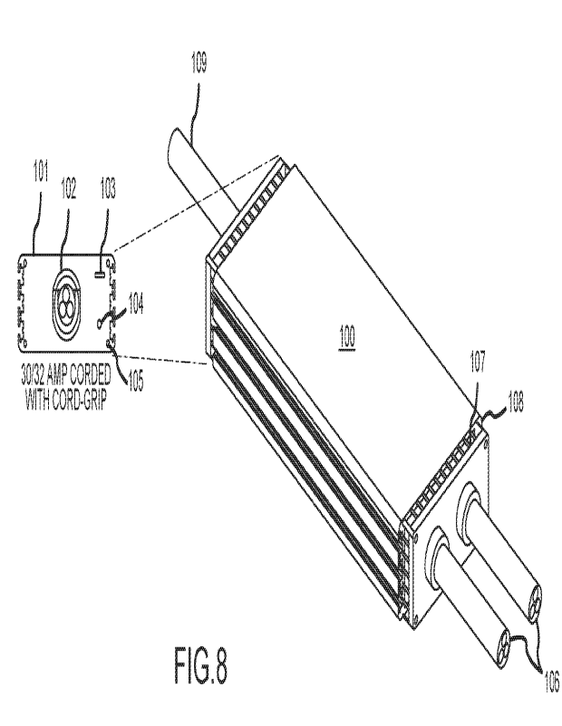
Figure 8 shows a 30 amp corded Automatic Transfer Switch in accordance with
the
present invention, shown in perspective and left end views;
13
CA 03189138 2023- 2- 10
WO 2022/035987
PCT/US2021/045589
Figure 9 shows a 30 amp dual IEC type C19 Output, Corded Input ATS in
accordance
with the present invention;
Figure 10 shows a 20 amp dual IEC type C20 Input, Single IEC type C19 Out ATS
in
accordance with the present invention;
Figure 11 shows a circuit and method for detecting zero crossings in
accordance with the
present invention;
Figure 12 shows how the synch detector circuit extracts the AC input voltage
valve in
accordance with the present invention;
Figure 13 shows a cross-section end view of the case of an ATS in accordance
with the
present invention;
Figure 14 shows components of a relay contact authentication detection module
in
accordance with the present invention;
Figures 15A-C show block diagrams of an ATS including relay operation
authentication
functionality in accordance with the present invention;
Figures 16A-16H show a circuit for implementing an inrush limiting function in
accordance with the present invention;
Figure 17 shows a high definition waveform sensor circuit in accordance with
the present
invention;
Figures 18-20 show a variety of instantiations of an ATS in accordance with
the present
invention;
Figure 21 shows a number of options for utilizing an ATS as described herein
to increase
the uptime and maintainability of an example SBC control module; and
Figure 22 shows a number of housing or case configurations in accordance with
the
present invention.
DETAILED DESCRIPTION
14
CA 03189138 2023- 2- 10
WO 2022/035987
PCT/US2021/045589
An automatic transfer switch system is described below that has a number of
advantageous characteristics relating to data conductivity, compact size,
avoiding use of valuable
rack space, primary power source selection, remote monitoring and reporting,
maximum current
control and the like. Specific examples embodying these advantageous
characteristics are
described below. However, it should be understood that alternative
implementations are possible
in accordance with the claimed invention. Accordingly, the following
description should be
understood as exemplary and not by way of limitation.
The primary function of the ATS is accomplished by transferring electrical
power from
one source to the other via a set of mechanical relays. In addition, the
closure of these
mechanical relays can be augmented by the use of modem semiconductor switches,
e.g.,
Insulated Gate Bipolar Transistors, (herein after referred to as IGBT) but
these devices could be
other semiconducting switches of sufficient Voltage and Current handling
capabilities in the
categories of TRIACS, SCRs, Bipolar Transistors, Field Effect Transistors, or
combinations of
each. These can be configured in a variety of ways, each with advantages and
disadvantages. A
preferred instantiation as applied to this ATS is utilizing IGBTs. They are
selected due to ease of
turning them on and off, robust construction, and resistance to false
conduction.
The timing and execution of desired functions is accomplished utilizing a
digital control
circuit comprised of a peripheral interface controller, or PIC. This device is
a member of the
"programmable function- devices and allows for a set of code to be recorded in
the device
that directs the actions of the overall digital control system. The PIC has
sufficient
computational capacity to perform certain mathematical computations to allow
for precision
calculation of voltages, current, time and other precision parameters
necessary for very
precise control of the timing of the relays and solid-state switches.
The ATS also includes advanced communication capabilities via a connection to
remote EDP equipment for the purpose of reporting status, electrical
characteristics of the
attached electrical -mains," and a variety of other information contents that
could be useful in
the maintenance of power systems attached to the ATS, either as source power
or as attached
equipment (herein after referred to as the "load-). This communication portal
on the ATS
utilizes as a primary means of communicating, the internationally accepted
schema called
Universal Serial Bus (USB), and as a secondary communication protocol of
PICKIT
programming transport. This secondary communication is included to allow field
upgrades
to be made without requiring the ATS device to be opened up for access to
traditional
programming ports. A third communications means is also provided that allows
simple
Digital Serial Data to be transmitted and received by the ATS via un-encoded 5
Volt logic
CA 03189138 2023- 2- 10
WO 2022/035987
PCT/US2021/045589
levels. This third communications means is provided to allow interfacing with
long-line
communications means. The USB transport and protocols are not especially well
suited to
transmitting and receiving data over distances greater than 10 to 30 meters.
For applications
requiring communication in harsh environments over long distances, an
interface is necessary
to convert the signals to various other standards. The availability of the raw
"serial data"
through the communication port enables the direct attachment of alternate
transport standards
interfaces simply and economically.
Description of Circuit Operation.
Figure 8 shows perspective and rear views of one instantiation of the ATS 100.
As
shown, two power cords 106 enter the ATS (A power and B power inputs) and one
cord 109
exits the ATS (power out to the load). It also shows that the ATS has
indicators 107 located
beneath a clear crenelated plastic lens 108 that also acts as the air inlets.
Shown also is the
aforementioned communication portal 103 and a small push-button 104 used for
inputting
some local control commands directly to the ATS.
The ATS 100 has a pair of small fans internal to the assembly that provide
cooling to
the various components inside as necessary. These fans are operated only as
needed and only
at what speed is necessary to maintain acceptable operating temperatures. Two
fans are
included for redundancy, and the controller inside the ATS 100 can report via
the
communications port to remote monitoring equipment any detected faults,
including the
performance characteristics of either of the fans. Temperature at the air
inlet of the unit as
well as the air outlet is also reported to the remote monitoring equipment.
Referring to Figure 7, The Overview of Basic Switching Concepts, a basic
understanding of the operation of the ATS can be gained.
= Figure 7A shows the off state of the ATS when no power is applied.
Switches 2, 3,
91 and 92 are all open.
= Figure 7B shows the state when power is applied to the A input. The unit
powers up
and the controller turns on the A input switch 2 and it also closes the Input
Selection Switch 4
(herein after referred to as the GK, short for Gate Keeper) and is allowed to
pass to the output
through the GKA switch 91. Power can now flow from the A input to the output.
= Figure 7C shows the state when power is applied to the B input The unit
powers up
and the controller turns on the B input switch 3 and it also closes the Input
Selection Switch 4
and is allowed to pass to the output through the GKB switch 92. Power can now
flow from
16
CA 03189138 2023- 2- 10
WO 2022/035987
PCT/US2021/045589
the A input to the output. When power is applied to both inputs, as will be
the normal
condition, then both of the Input Selection Switches will close and deliver
power to the GK 4
where the controller will direct either the GKA switch 91 or the GKB switch 92
to gate
power to the output. Never should both GKA 91 and GKB 92 ever be closed at the
same
time. This will result in shorting the two inputs together.
= Figure 7D shows the condition of having both GKA 91 and GKB 92 on at the
same
time. A fuse located on one side of the A input 12 is shown -blown" or open,
in this case.
Since the GK has shorted both leads of A input to B input, then the opposing
side must also
be protected. The B input also has a fuse 13 on one of its inputs, but it is
in the opposite lead
path. It is also shown "blown," or open. These two fuses 12, 13 not only
protect the load
from exposing the circuit to a dangerous condition, but they also prevent a
serious overload
of the input power sources in the unlikely event of a catastrophic internal
failure of the ATS.
Using this technique, two fuses can protect all 6 leads, two on the A input,
two on the B input
and two on the Output, with any overload condition in any combination.
= Figure 7E shows the introduction of the Solid State Switching elements
93, 94.
Mechanical relays all require some finite amount of time to operate after the
signal is applied
to the coil, either to close or to open the contacts. Solid State Switching
devices generally
have a very short time to operate, on the order of microseconds. However, they
do exhibit a
voltage drop across the junction when conducting (closed) and this voltage
drop represents
loss of power in the circuit. For example, an IGBT based semiconductor AC
switch (such as
applied in this instantiation) exhibits a voltage drop of about 3 volts at 30
Amps of conducted
power. That relates to 90 Watts of loss. The equivalent mechanical relay will
exhibit a loss
of about 1 Watt at the same applied current. Thus, a mechanical relay
augmented with a solid
state relay is an ideal combination for maximizing efficiency as well as
operation speed.
When desired to conduct, an augmented relay configuration as shown in Figure
7E, the
conduction of electrical current will commence within about 10 microseconds of
the
command to conduct. This allows precise timing of the connection to the power
source.
However, the disconnect time is still subject to the response time of the
mechanical relay
since the contacts of the mechanical relay are in parallel connection to the
SSR element.
Even though the SSR element may disconnect, the mechanical contacts will
remain closed for
a short time prior to releasing. This delay is of little consequence when
switching from one
power source to the other when power is available on both, such as is the case
when the ATS
is returning to the preferred side after the power has been restored on that
preferred side.
17
CA 03189138 2023- 2- 10
WO 2022/035987
PCT/US2021/045589
Precise timing of the disconnect can be accomplished in this case because the
mechanical
relay can be commanded to release prior to the desired time of the actual
disconnection, while
the SSR is still conducting. Then, at the desired time of disconnection. the
SSR can be
commanded to release. Thus, for most conditions, precise timing can be
achieved, with little
power loss in this configuration. The use of the IGBT and bridge AC switch has
the
advantage of being able to turn on and off in very short time periods. It is
difficult to turn off
a Triac, or an SCR based switch, as those devices want to stay on until
current stops
conducting, thus they stay on until the AC current passes through the zero
crossing as the sine
wave changes polarity. In the example shown in Figure 7E, The SSR on side A 93
is shown
in the on condition, and conducting power to the Output while the mechanical
relay contacts
of GKA 91 are moving to try to close. Any variation in timing that might be
imposed by the
mechanical effects of the motion of the relay contacts are masked by the SSR
conducting.
Albeit the associated power loss intrinsic to the SSR delivering the current
is present during
this time, it is of only a very short duration, about 10 milliseconds, before
the mechanical
relay contacts close, thus reducing the power loss to a minimum. The SSR can
remain on but
it will have no effect.
= Figure 7F shows the final configuration with power being conducted
through the
GKA relay 91 to the output and bypassing the SSR 93.
Sub-circuit Detailed Descriptions
Figure 1 shows the general configuration of all of the sub-circuits and helps
identify their
function in the overall operation of the ATS. Note that both the A side AC
power connection and
the B side AC power connections pass through a -N" Side Disconnect and Sync
Generation sub-
circuits 2,3. When AC voltage is not present on the input to one or both of
these circuits 2,3 the
internal mechanical relay inside of this circuit remains in the "open- state,
thus no power is
passed through to the Gate Keeper 4. These "N" Side Disconnect and Sync
Generation sub-
circuits 2, 3 provide several functions to the operation of the ATS.
Disconnection from the GK 4 when power is not present on the input provides
safety
disconnection from the source and provides required disconnection isolation
voltage capacity
required by various safety agencies such as Underwriters Laboratory (UL). The
mechanical gap
on the relay contacts prevent voltages as high as 3000 Volts from passing
through.
Commands from the Digital Control Electronics 1 can command the -IN¨ Side
Disconnect and
Sync Generation sub-circuits 2, 3 to engage or dis-engage, as timing needs are
satisfied.
18
CA 03189138 2023- 2- 10
WO 2022/035987
PCT/US2021/045589
The "N" Side Disconnect and Sync Generation sub-circuits 2, 3 also have a
circuit in them that
detects the AC voltage near the point where it crosses zero when changing from
one polarity to
the other. This signal generation allows a pulse to be generated that is
symmetrical about the zero
crossing to be formed and sent to the Digital Control Electronics 4 for use in
providing
information needed to electronically synchronize and control the various
actions of the ATS.
= Figure 11 shows the simplified means that this is accomplished in the "N"
Side
Disconnect and Sync Generation sub-circuit. The circuit 200 is comprised of
three main
elements, the input bridge 202, comparator 203 and isolation optical coupler
205. As AC
voltage is applied to the input 201 it becomes rectified in the bridge 202.
The rectified
voltage is scaled down to a useable voltage by resistor divider R1 and R2 and
that voltage
is applied to the input of the comparator 203. The other input of the
comparator 203 has a
reference voltage applied to it formed by the resistor divider R3 and R4 and
is filtered by
the capacitor Cl. When the applied rectified voltage from the AC bridge
becomes greater
that the reference voltage, the output of the comparator 203 switches "On," in
this case
the output goes to 5 volts, or High. When the applied rectified voltage from
the AC
bridge becomes less that the reference voltage, the output of the comparator
203 switches
"Off', in this case the output goes to 0 volts, or Low.
= The synchograms 300 show the voltage ¨ time waveforms typical of this
circuit
200. The AC In 207 is rectified 208, and when the thresholds are crossed, the
output of
the comparator produce pulses 209 at the point where the original AC in 207
crosses at
the zero crossing plus the threshold of the comparator. These pulses are
nearly
symmetrical about the actual zero crossing of the original AC In voltage.
The Sync pulse formed in "N- Side Disconnect and Sync Generation sub-circuits
2, 3 also carries
information about the applied voltage to that circuit in the form of the pulse
width. As the
voltage increases the pulse width becomes narrower and narrower. This allows
detection of the
applied voltage by the Digital Control Electronics on the same signal path as
the synchronization
pulse.
= Figure 12 shows how the sync detector circuit also functions for
extracting the
AC Input Voltage value in the Digital Control Electronics Section. Assuming a
high
voltage of, for example, 240 VAC, is represented by the synchogram 300 at the
AC In
207. The rectified Voltage 208 is then crossing the threshold and results in
pulses 209
formed that are narrow. But, if a lower voltage, say 120 VAC is applied as
shown in the
second synchogram 301 the voltage threshold of the rectified AC voltage 221 is
crossed
19
CA 03189138 2023- 2- 10
WO 2022/035987
PCT/US2021/045589
sooner and as a result the Comparator Out 222 pulses become wider. The Digital
Control
Electronics can compare the time of the rising edge to the falling edge of
these pulses and
apply mathematical formulae to retrieve the exact voltage that is represented
by those
pulse widths. Alternatively, the Digital Control Electronics can hold a table
of
representative values that, when compared to the detected pulse width times,
can also
result in very accurate representations of the applied voltages.
The output of the comparator circuit in the "1\1- Side Disconnect and Sync
Generation sub-
circuits is passed through an optical isolation circuit to make sure that the
Digital Control
Electronics is electrically isolated from any AC or DC Voltage applied to the
inputs. This is a
safety requirement and is enforced by various regulatory agencies such as
Underwriters
Laboratory (UL).
= Figure 2B shows the schematic of the "IN" Side Disconnect and Sync
Generation
sub-circuits. The AC filter section 21 shows a simple Pi filter attaching the
AC mains to
the electronics of the "N" Side Disconnect and Sync Generation sub-circuit via
a fuse F5
of 250 ma. A pair of inductor and a capacitor are used to prevent any high
frequency
noise generated in the attached circuits 22 from entering the AC mains lines.
This is done
to prevent interference with other external electric and electronic devices.
This is also
necessary for various compliance agencies such as Federal Communication
Commission,
of FCC, as well as others. After power is filtered, it is delivered to the
Switchmode
Current Limiter 22 where the AC high voltage is rectified in D2, D3 D8 and D9
and
delivered to the filter capacitor C2 via D4. D4 isolates the rectified DC from
the bridge
from the filtered DC of C2. The un-filtered rectified DC is delivered to the
comparator
through the resistive divider R6 and R5 for developing sync and voltage data
as
previously described. Rectified and filtered DC voltage at C2 is delivered to
the
Switching chip Q9 via a filter inductor pair of L10, a ferrite bead for very
high
frequencies, and L12, for medium frequency limiting. The switching chip Q9
turns on
and off at about 80 Khz, and the duty cycle determines how much current is
present in
Ll. Since this is switching into Li from a monopolar source, the flyback
energy in Li is
contained by D10. The Switching chip chip Q9 is pre-programmed to adjust the
duty
cycle to maintain a constant current of 20 ma. This chip is originally
designed for use in
modern LED lighting, but is r purposed to simplify the power supply design of
this
invention. The varying pulses in Li are translated to a fairly constant
current of 20 ma
and then is allowed to pass through the coils of the two relays 21 that switch
on the main
AC power. The other side of the two relay coils 21 enter the On-Off Switch 23
at the
CA 03189138 2023- 2- 10
WO 2022/035987
PCT/US2021/045589
Drain of Q5. If Q5 is "On," the current then passes to the secondary filter
capacitor C7 In
the Sync Pulse Generator section 25. 20 ma oy current is presented to the
Cathode of
ZD3, and when the voltage reaches 8.2 Volts, the Zener conducts to maintain
about 8.2
Volts. This voltage is presented to the input of the 5-volt regulator Q7. This
is a
precision 5-volt linear regulator. As long as the total power requirements of
the output of
the regulator, and the attached circuits does not exceed 20 mA, then ample
overhead
voltage will be present to maintain precision 5-volt regulation. The design of
the Sync
Pulse Generator 25 Comparator circuit is such that there is very little
current necessary to
accomplish the detection function. Only about 2 mA is actually used in this
part of the
circuit. This leaves 18 ma available. Some of the 18 mA available at the input
to the 5
volt regulator Q7, is diverted to the opto-coupler U4 26 and through the 1K
resistor
connected to the output of the comparator U7. If the U-7 is in worst case
voltage
detection mode, where the output is "on" (or low) all of the time, then all
8.2 Volts is
dropping through the 1 K resistor, minus the 2 volt drop of the LED in the
opto coupler
U4. The resultant maximum current is 6.2 mA. Thus, for all cases, the series
switch
mode regulation of a total of 20 mA, is adequate to drive all possible
combination of
circuit requirements.
This method was chosen to optimize the efficiency of operation of the
circuits. Very little
power is wasted, and the total circuit power efficiency is about 84%. The
total quiescent
power used to operate the "N- Side Disconnect and Sync Generation sub-circuit
is about
_65 Watt. Both the A and B sides add up to around 1_3 Watts. This is a very
high
efficiency for all of the functions achieved.
This scheme also makes the operation of these circuits functional from about
30 Volts of
AC applied to the mains inputs all the way up to 300 Volts. These circuits
must function
across the maximum range of AC input voltages to allow monitoring and
functionality of
the ATS regardless of the voltage applied.
A signal that comes from the Digital Control Electronics, "Force Disconnect"
27 is
presented in cases where the Controller wishes to shut off an input. This is
done during every
transfer cycle to prevent any possibility of carrying an arc between the
contacts of the Gate
Keeper (Figure 3, 39 and 40) that would cause a short between the A side and
the B side Power
Inputs.
The "Force Disconnect" 27 signal causes the LED in the opto-coupler Ul to turn
on the
phototransistor in Ul , which in turn shorts the Gate of Q5 to the Source of
Q5. This turns the Q5
21
CA 03189138 2023- 2- 10
WO 2022/035987
PCT/US2021/045589
Drain off and shuts off the current path to the relays. About 2 ins. Later the
relay contacts open
and power is disconnected between the input and the output of the Disconnect
relays 21.
When the -Force Disconnect" is removed from the opto coupler Ul, and the
phototransistor turns off, then current from R1, 3.9 Meg ohm resistor is
applied to the gate of Q5,
the voltage rises to about 10 volts very quickly and the Drain of Q5 is
connected to the Source
and Q5 is turned on. Current can now pass through the coils of the switching
relays, sourced by
the switch mode chip Q9, as described earlier. The relays 21 are now energized
and the contacts
are closed about 7 to 10 ms later.
During the time that a "Force Disconnect" is present, there is no need for
sync pulses
during the transfer process. Voltage and timing have already been determined
by the Digital
Control Electronics. But a "Force Disconnect" usually only lasts for 20 ms or
so, just long
enough to complete a transfer. During that 20 ms, power stored in C15 keeps
the comparator
operational, and pulses can continue to be detected if there ever became a
need to utilize the
information.
Figure 3 shows the detailed block diagram of the Input Selector, or Gate
Keeper (GK). This is the
core of the ATS. This is where power from either the A side Disconnect Switch,
of the B side
Disconnect Switch is directed to the Output and eventually to the "load". Its
operation is directed
entirely by the commands from the Digital Control Electronics. When no signals
are present
from the Digital Control Electronics all of the relays in the GK, and the
Solid State Relays (SSRs)
are in the open, non-conducting state. This presents a "Fail Safe- condition.
In order for the Digital Control Electronics to direct power from the A Side
Disconnect
Switch output, it must first make sure that no control signal is being sent to
the B side steering
circuits. A special piece of code in the Digital Control Electronics makes
this check every time a
attempt to change the state of either input is made. It is critical that the A
side and the B side are
never connected to the output at the same time, as this would result in a
short circuit between the
A side and the B side inputs and would cause a fuse to blow, and perhaps more
damage. A
second layer of protection is included with the implementation of hardware
interlock 49 that
prevents two commands from conflicting. For example, if the Digital Control
Electronics
requests that the A relay coil driver turns on by asserting the control line
42, that signal will also
be present at the input of the logic gate 46. Since the true state of the A
side request is inverted at
the input to the logic gate 46, any signals present at 41, the control line
that would drive the B
side, is blocked by the gate 46. Conversely, a signal from the Digital Control
Electronics
requesting to turn on the B side Relay Coil Driver 41 that is asserted will be
present at the
inverting input to the logic gate 43 and in turn mask any signals coming from
the A side Digital
22
CA 03189138 2023- 2- 10
WO 2022/035987
PCT/US2021/045589
Control Electronics conunand 42 to turn on the A side Relay Coil Driver. The
same concepts
apply to the IGBT drivers. These function similarly to the Relays, but with
nearly instantaneous
response times. The commands to turn on one side or the other will result in a
masking signal
sent to the opposite side and prevent a dual turn on condition to exist. A
"high" in the IGBT drive
A side control input 47 will be presented as a low to the gate on the b side
45 and inhibit any
signaling from the Digital Control Electronics from passing through the gate
45. Conversely, A
"high- in the IGBT drive B side control input 48 will be presented as a low to
the gate on the b
side 44 and inhibit any signaling from the Digital Control Electronics from
passing through the
gate 44. 5 KV Optical Isolators are included between the Digital Control
Electronics and the
IGBT Drivers. This is necessary since the IGBT drivers operate at the AC Line
voltage potential
of their respective AC sources. The Relay Coil Drivers do not require
isolation, the Coils of the
relays 39, 40 are isolated from the AC Line voltage mechanically.
Figure 3B shows the detailed Electronic Schematic of the Input Selector, or
Gate Keeper
(GK). When the Digital Control Electronics determines that the A side AC power
should be
connected to the Output, it simply asserts both the Gate Keeper o A (GK to A)
signal and IGBT
Drive A. The 5 volts logic control signal presented at GK to A will turn on
the FET Q11. It's
Source is connected to ground, so the Drain goes to ground, thus supplying
current to the coils of
the A side Gate Keeper relays, RY 3 and RY 7 These relays acquire coil current
from the +12
Volt power supply. Magnetic field current starts to build in the coils and the
relay is starts to
energize. Generally speaking these relays require 7 to 10 ms to operate. The
bigger the relay, the
slower the operation, generally. During this time the second half of the
operation has begun. The
Digital Control Electronics has also issued a assert command to the IGBT Drive
A input. This
High level (5 Volts) signal sends current to the LEDs of U 13 and U 15, 5 KV
Isolation opto-
couplers, via resistors 27 and 28. This current is dependent on Q14 a PNP
bipolar transistor
being turned on also. The turn on of Q4 is generally present due to the base
pull down resistor
R31. If, for some reason, the IGBT Drive B was high (asserted for some
reason), the base of Q
14 would also be high, and no current would be able to go through the
collector of Q14, thus
disabling the IGBT Drive A command. The transistor Q14 is essentially the
logic gate discussed
prior with Figure 3A, Logic Gate 44. This is the second layer fail-safe
discussed earlier.
However, assuming that the IGBT Drive B is not asserted, and that the IGBT
Drive A is asserted,
and that current is now flowing in U 15 and U 13, the other side of those opto-
couplers will now
be also conducting.
To understand how the TGBT drivers turn on the IGBT, it must be assumed that
AC
power has been present coming from the A Side Disconnect Switch for at least a
little while.
23
CA 03189138 2023- 2- 10
WO 2022/035987
PCT/US2021/045589
That AC Voltage that has been present has been conducting through Diodes 13
and 32, and R 41
and R3, charging Capacitors 26 and 32, each to 20 Volts. When these capacitors
reach 20 Volts,
the current is diverted through Zener Diodes ZD 5 and ZD 1, and the voltage
remains at 20 Volts.
The capacitors are 4.7 micro-Farads each. The amount of charge they hold is
important later on
in the discussion.
When the optical coupler photo transistor in U13 turns on, 20 volts from C26
will be
conducted through R9 and on to the base of Q13 and resistor 2. Capacitor 33
presents a very
short impedance to this turn on and filter out transient noise. Otherwise,
Capacitor 33 has no
effect. When the voltage is applied to the base of Q13, the voltage rises very
fast, limited
essentially by the charge rate of C33. As the Base of Q 13 rises, the
transistor releases its current
path from the Emitter to the Collector, essentially shutting off this
transistor. The rising voltage
at the base of Q 13 now is passed to the base of the IGBT Q2 via the diode 21.
These rising
voltages are now limited by the base capacitance of the IGBT Q2 and the
current limiting of the
Opto coupler and R33. Since the opto coupler is around 200 ohms at this time,
the rise time is
relatively fast, on the order of 150 microseconds. The IGBT Q2 is now
conducting. Any AC
Voltage that appears across the contacts of the RY7 at this time is shunted
through the Diode
Bridge BR2 and through the IGBT Q2 Collector- Emitter. Effectively, the AC
inputs to the
bridge BR3 are shorted. This whole process has taken about 200 micro-seconds.
Meanwhile, the
Relay 7 is just starting to energize. It will be another 7 to 10 ms before it
actually has the contacts
meet one another. The AC input to this side of the Load is now connected.
The same process is occurring on the other half of the A side IGBT drive, the
side driven
by U15. Ultimately, IGBT Q3 will be turned on, shunting Bridge 3 and
delivering AC power to
the other side of the A side path between the A side Disconnect Switch to the
Output and to the
load.
After a period of around 100 ins, it is assumed that the relays have closed
and that all of
the current is bypassing the IGBTs. The Digital Control Electronics will de-
assert the IGBT
Drive A and the IGBT Drive B control signals. If, for some reason the Digital
Control
Electronics did not release the drive signals, a designed in feature of the
IGBT Drivers
themselves will release the drive signal from the IGBT gates and disconnect
the devices. This is
accomplished by the decay of the stored charge in the aforementioned C26 and
C32. The current
path from the C26 and C32, through the opto couplers and through the 68 K base
resistors for Q
13 and Q 21will eventually discharge the C26 and C32 to the point where the
IGBTs do not have
sufficient voltage on the Gates of these devices to sustain current flow in
the Collector to Emitters
of Q 2 and Q3. Even though some current is being supplied to the C 26 and C32
from the D13
24
CA 03189138 2023- 2- 10
WO 2022/035987
PCT/US2021/045589
and D32, the resistive divider of 560K and 68 K, through a half wave
rectifier, will not provide
sufficient voltage at the base of the IGBTs to sustain current. At maximum
input voltage to the
ATS of 277 volts AC, only about 6 volts will be present at the gate of the
IGBT and the device
will turn off Careful selection of components has enabled this feature without
the addition of
any additional circuitry.
When the Digital Control Electronics determines it is time to shut off a
particular side of
the GK, there are two possibilities. One is for an immediate shut off,
implying it is being turned
off as fast as possible due to a loss of voltage on this path. This would be
the case when, for
example, this is the A side, the A side is the preferred, and the load has
been connected to the A
side for some time. This is a normal state.
When the A input AC voltage fails below an acceptable level, the control logic
can
determine that the A input power is failing and an outage (vs. a power quality
disturbance for
example) is in progress. It is now necessary to transfer to the alternate
power source (the B side in
this example) as fast as possible. The first action to consider after the
Digital Control Electronics
has determined that the failure is valid by observing the a Sync pulse
occurred at a time it
shouldn't have, or the sync pulse was longer than it should be, the Digital
Control Electronics will
immediately start the disconnect process. It is paramount that the failed AC
power input be
totally disconnected from the output prior to connecting the alternate side
power source to the
Load. Otherwise, current would be transferred from the Alternate power Source
to the Primary
power source, which could be at a very low impedance (for example, the whole
AC grid). So,
knowing that it has taken a couple of milliseconds to verify that a failure
has happened, another
two milliseconds (plus a little buffer insurance of 1 millisecond) is
desirable to ensure that the
Input Relays and the Gatekeeper Relays have had sufficient time to
mechanically open. As
mentioned before, this time is on the order of 2 milliseconds average. Thus,
the command to
"Force Disconnect" the primary side (A in this example) is immediately issued
along with the
GK to A control lead being de-asserted. This starts the process of
disconnecting from the A side.
It is assumed that the IGBT Drive for the A side has long since been removed,
preferably about
200 ms after it was asserted long ago when power was initially transferred to
the Primary side.
The Digital Control Electronics must now wait patiently for at least two
milliseconds.
The ATS Digital Control Electronics actually waits 3.5 ms, with the relays we
are currently
using, but this value is programmable into the Digital Control Electronics and
may change
depending on the relays sourced for use in these ATS units. But it does wait
until it is sure that
enough time has passed that the mechanical relays have opened the path from
the previously
connected Power source and the output. At this point, The Digital Control
Electronics can assert
CA 03189138 2023- 2- 10
WO 2022/035987
PCT/US2021/045589
the IGBT Drive B and the GK to B signals and connect the load to the alternate
power source as
described in the connect sequence above.
When the IGBT drive is off, and the opto-couplers are not turned on, there is
no current
source to keep C33 (C47) charged and they decay in voltage down from wherever
they were until
these capacitors are fully discharged via resistors R2 and R4. At this point,
the bases of Q 13 and
Q21 are at the collector potential. Q13 and Q21 are Darlington coupled
transistors and have gain
characteristics in excess of 20,000. Any attempt to raise the voltage on the
emitters of these
transistors Q13 and Q21, will result in immediate conduction to the collector
potential. In other
words, the Gates of the IGBTs Q 2 and Q3 are shorted to their Emitters. This
is necessary.
Because the Collectors are connected indirectly to the output of the ATS via
the Bridges BR2 and
BR3, when the IGBTs on the Alternate side do come on, and deliver AC to the
Load from that
side, they will turn on very fast. The resultant very high rate of voltage
change at the output will
appear at the Collectors of the now off IGBTs Q2 and Q3. Without the very low
impedance
clamp on the Gates of the 1GBTs Q2 and Q2, the high rate of rise at the
Collectors will try to turn
on the IGBTs through the capacitive coupling internal to the devices. The
higher the rate of rise
of the voltage, the more susceptible the IGBTs are to false turn on. Thus, the
ever-present clamp
across the Gate to Emitters of the IGBTs when they are off This unique IGBT
drive scheme is
both simple and robust. It requires no external power to operate. Switching on
the alternate side
from IGBT Drive B and GK to B are mirrored in function to the A side.
Figure 4 shows how the ATS monitors current and retrieves data necessary for
synchronization of zero crossing using the output current As an ATS, the
decision to transfer a
load from one active AC power source to another active AC power source
requires additional
considerations other than performing the transfer as quickly as possible.
Since both AC sources
are present, there may be additional considerations to make when deciding when
to disconnect
from the active source delivering power to the load, and then connecting it to
the active AC
source that is considered the Primary source. This event occurs every time
there is a power
outage on the primary source, the ATS transfers to the alternate source, and
then eventually the
Primary AC power source is restored. AT this time, the transfer the ATS must
make is from one
good source to another good source.
It is necessary to make the opening of the relay occur at or near the zero
crossing of
current when disconnecting a load from an active AC source. This helps fervent
contact arcing
and extends the life of the relay contacts. In the ATS described here, the
Disconnect Relays in
the Disconnect Switch and Sync Section do not have solid state bypass circuits
to unload the
26
CA 03189138 2023- 2- 10
WO 2022/035987
PCT/US2021/045589
CLUTelli from the relay contacts during a disconnect. Thus, the disconnection
must be
synchronized with the zero crossing of the current in the circuit.
The ATS described herein can deliver power to a variety of load types. One
such load
type is what is referred to as a reactive load, often found where the load has
capacitance,
inductance, or a combination of both. When there is capacitance or inductance
in the circuit,
the voltage and current waveforms are not synchronous. The power flow has two
components
- one component flows from source to load and can perform work at the load and
the other
component known as the "reactive power", is due to the delay between voltage
and current,
referred to as phase angle, and does not do useful work at the load. It can be
thought of as
current that is arriving at the wrong time (too late or too early). This phase
difference between
the actual voltage zero crossing and the zero crossing of the current requires
that, since the relay
contacts can be damaged by current, not volts, it becomes necessary to cause
the relay contacts to
open at the time that the current is passing through the zero. Since this can
be different timing
from the zero-crossing detected in the Disconnect Switch and Sync Section. an
alternate method
of determining the timing of the relay opening, and it must be based on the
current flow instead of
the voltage present.
When power is present on both sources, and a transfer is imminent, the Digital
Control
Electronics must measure the output current, and if it is significant, use
this to determine when to
open the various relays in the path of the current flow. In the ATS described
here the Digital
Control Electronics has tables loaded into its memory at the time of
manufacture that contain the
measured time between the command to release a given relay, and when it
successfully opens the
contacts. Generally, this time is about 2 milliseconds, but it can vary
significantly due to
manufacturing variables. Thus, the Digital Control Electronics keeps track of
the delay times for
each of the relays in the ATS and can use that information to calculate the
exact disconnect time
when preparing to disconnect the load from an active AC source.
The Digital Control Electronics also has determined the time from one-half
cycle to the
next by measuring the rising edge to the rising edge of the sync pulses
generated in the
Disconnect Switch and Sync Section. By using this information, the Digital
Control Electronics
can now subtract the known delay of a given relay from the time between half
cycles and arrive at
a number that is predictive of when the relay contacts will start to open,
relative to a zero crossing
of current. The Digital Control Electronics will prepare to make the relay
opening, then at the
next zero crossing of the current will then delay the amount of time
calculated by subtracting the
relay opening time from the half cycle to half cycle time, then the Digital
Control Electronics
issues the disconnect command.
27
CA 03189138 2023- 2- 10
WO 2022/035987
PCT/US2021/045589
In this manner, the ATS described here can disconnect a load very close to the
actual zero
crossing of the current by performing these predictive calculations. This
minimizes the
degradation of the electrical contacts within the relays. In addition,
conditions could exist that
prevent a relay contact from releasing when the command from the Digital
Control Electronics
commands it to disconnect. The most common cause of this is a welded contact
that is the result
of some excessive current during the prior transfer. Other conditions could
include mechanical
wear or degradation of materials due to time, heat or other causes. In any of
the cases where a
contact has not operated in the manner desired by the Digital Control
Electronics, a method is
described here that allows the Digital Control Electronics to detect that
fault condition. If the
fault condition is detected before the commands are issued for any additional
relay or SSR action,
then a shorting of the A side power source to the B side power source can be
avoided. In much
large Automatic Transfer Switch applications, traditional ATS designs, this is
accomplished by
mechanically linking the power contacts of the relay to an auxiliary set of
contacts that can be
monitored by the Digital Control Electronics for this authentication process.
In the case of the
MINI ATS application described here the physical size is of significant
concern. A novel means
of detecting the operation of the relay is described here, referred to as the
Relay Operation
Authentication Detector, that allows this authentication, while maintaining a
small form factor.
In addition, this detection means is directly involving the active electrical
conductive portion of
the relay that actually passes the power through the relay. By detecting on
that specific electrical
conductor, there is positive confirmation of the state of that contact, either
connected to the power
source or not connected. When the Digital Control Electronics commands either
the closure of
the desired relay or opening of the desired relay, this authentication feature
allows the Digital
Control Electronics to immediately check the results of that action request
and verify it has
completed before moving on to performing any other actions. In the event of
detecting a failure
to complete the command by the relay in question, the Digital Control
Electronics can then
undergo a process to halt any additional actions, report this fault event to
the monitoring
controller, and it can perform multiple attempts to operate the relay and
possibly self-repair the
electrical fault by breaking loose the potentially welded contact. In that
event, the Digital Control
Electronics can then elect to return the entire MINI ATS to operation or place
it in a safe state
such as totally shut down. The determination of what to do with the fault
condition is fully
programmable and can be specific to various applications. This flexibility
offered by
implementing the authentication is unique in Automatic Transfer Switches.
In addition, the authentication circuits allow the Digital Control Electronics
to operate in a
mode where the next step is not determined by time as described earlier, but
by what state the
28
CA 03189138 2023- 2- 10
WO 2022/035987
PCT/US2021/045589
various components are physically, or electrically in. For example, when the
conunand to
disconnect the relay from one source is issued, instead of calculation when it
should have
disconnected, to allow proceeding, the Digital Control Electronics simply
waits for the
authentication signals from the affected relays to indicate a successful
completion of the action.
The Digital Control Electronics merely has to put a timed limit on that so
detection of a fault can
be determined. But being a state-controlled process means that the next action
that is dependent
on the upcoming change of state is timed to the optimum time when that next
action can
commence.
Figure 4 shows the basic electrical and electronic components of the Current
sensing
section of the ATS. The primary sensing element is a Hall Effect sensor 51
adjacent to the Hot
Out Lead that is attached to the output of the ATS. The magnetic fields
generated by the passing
current 57 is detected in the Hall effect sensor 51and amplified. Zero
restoration 52 of the sensed
signal is necessary to stabilize the conversion from AC measurement to DC in
the Precision
Rectifier 52. After the Current waveform has been rectified, it is still
returning to zero every half
cycle. At the moment it returns to zero, the Zero Crossing Detector 55 output
asserts. This signal
is sent to the Digital Control Electronics for use in calculating timing. In
addition, the rectified
current output of the Precision Rectifier 52 is also sent to an integrator
that consists of an array of
capacitors and resistors that smooth out the sensed current and convert it to
a smooth DC level.
That DC level then is sent to the Digital Control Electronics via a buffer
amplifier and enters the
Digital Control Electronics through an integrated Analog to Digital Converter
for digital
processing and reporting of the current levels to the communication port, and
eventually to the
remote monitoring equipment.
The Digital Control Electronics also uses the integrated DC levels to
determine if the
ATS should turn on the light that warns of "maximum load acceptable." A
feature of the ATS
described here is its ability to set a warning light when the load is above a
pre-programmed level.
Another action that the Digital Control Electronics can perform using the
integrated DC
level is to shut off the output in the event of an overload. If the current
exceeds a pre-
programmed level, the ATS can de-energize the Gate Keeper relay very quickly
to protect the AC
power circuit. The Digital Control Electronics can then turn on another
warning light to indicate
that an overload has occurred, and it can send status data through the
communication port to the
remote monitoring equipment.
Another feature of the ATS described here is its ability to set a warning
light when the
load exceeds a pre-programmed level and turn off power to that load
coincidentally.
29
CA 03189138 2023- 2- 10
WO 2022/035987
PCT/US2021/045589
A reset button (Figures 8, 9, 10, item 104) is provided as a means for the
operator to reset
a Load-Fault condition once the fault has been removed.
Unique filtering at the hardware level in the integrator 54 and software
computations by
the Digital Control Electronics allow a precise imitation of any fuse curve
desired, or any circuit
breaker desired.
The output current sense discriminated by the Digital Control Electronics can
also be
used to predictively operate the cooling fans. Instead of waiting until the
interior of the ATS has
heated up due to heavy loading, and then turning on the fans, the Digital
Control Electronics can
predict the internal heating due to detected load in the current sensor 11.
Thus, the fans come on
before individual components become hot. This feature can be useful in
improving the reliability
of the ATS.
The ATS can be predictive about internal heating and start the fan(s)
proactively to
reduce materials fatigue and improve reliability.
Figure 5 shows the overview of the Indicators 9 in the ATS, and the
Communication port
10.
The Indicators are generic LEDs of various colors. Utilizing state-of-the-art
components,
bright and efficient LEDs provide excellent indications of the various
statuses of the ATS
described here. The unique crenelated lens assembly allows effective airflow
as well as an
excellent range of angles of visibility of the LEDs.
In addition, a current limiter 60 is in the path of the electrical supply for
all of the LEDs.
This prevents overloading of the power supply in the event that 3 or more LEDs
are illuminated
simultaneously.
The Communication portal 10 provides a specialized communication set between
the
Digital Control Electronics and the remote monitoring and control electronics.
Three functions are provided by this port, but others could also be
implemented.
i. USB communication with the remote monitoring and control electronics.
ii. Connection between the Peripheral Interface Controller (PIC) (a type of
MCU) internal to the
ATS described here, and an external programming tool. This allows updating the
software
(firmware) of the PIC without having to open the case up. There may be
customers that have
ATSs as described here that require special functions. Due to the unique
design of this ATS,
these client needs may be met by supplying specialized operating code to the
Digital Control
Electronics of this ATS.
CA 03189138 2023- 2- 10
WO 2022/035987
PCT/US2021/045589
iii. Connection between the Digital Control Electronics and external
conununication interface
converters to allow long line communications to remote monitoring and control
electronics. USB
has short length limitations and as such may not be applicable to all
communications
requirements.
The Digital Control Electronics can send data via USB to the remote monitoring
and
control electronics via the USB 2.0 interface converter 71 through the panel
accessed USB type C
connector 72. A USB type C connector is selected for its unique pairing of
pins that generally
allow the connector to be mated in either polarity. The pins from one side of
the connector are
mirrored on the other side of the connector so that regardless of which way
the mating connector
is inserted, the communication and voltages sent through the connector system
will be preserved.
The ATS described here leverages this bi-polar characteristic for an added
feature. By flipping
the connector, that flip can be detected and send an alert signal 76 to the
Digital Control
Electronics via a Polarity Detect circuit 70. The Polarity Detect circuit
operates by detecting if a
ground pin is present on one of the pins. The complement pin (in a reversed
condition of mating
the connectors) is connected, instead, to the +5 volts pin of the connector.
In this manner, the
orientation of the connector can be determined by the Digital Control
Electronics. This is useful
by allowing the Digital Control Electronics to determine if it should be
communicating via USB,
or if it should be preparing to accept data from a remote programming tool.
This feature also can
be used to alert the operator that the connector is flipped. This can be used
to help improve the
security of the data contained in the Digital Control Electronics. By flipping
the connector one
way, a physical barrier to writing data into the Digital Control Electronics.
However, flipping the
connector the other way allows data to be written to the Digital Control
Electronics, while
simultaneously the Digital Control Electronics can provide distinctive
illumination to the LEDs
that alert the operator to this write vulnerability.
Thus, the unique wiring of the USB type C connector allows the ATS described
here to
communicate with multiple types of external electronics and improve the
security of the data
stored in the ATS.
Figure 6 shows the overview of the power supply system in the ATS described
here.
Since it is unknown at any time if power will be present on the A input, the B
input or both, a
power supply system is included that is both 5 KV isolated from the Digital
Control Electronics,
but it is available from both the A and B inputs. A 12-volt DC supply is
attached to the output of
the A Side Disconnect and Sync AC Power out. Also a 12-volt DC supply is
attached to the
output of the B Side Disconnect and Sync AC Power out. Each of these power
supplies are
31
CA 03189138 2023- 2- 10
WO 2022/035987
PCT/US2021/045589
connected to a common +12 bus via isolation diodes 86 that are contained
within the power
supply modules. These diodes provide the capability of either power supply to
operate if one or
the other fails. This is a redundant power supply system and is an added
feature of the ATS
described here.
The 12-volt bus is distributed to the various electronics on Digital Control
Electronics 1
and the A or B Side Selector 4 electronics where the 12 Volts DC is reduced,
if needed, to 5 Volts
and 3.3 Volts as necessary with local regulator chips. The inputs to the 12
Volt power supplies
are protected by fuses 89, 90 for safety reasons.
In addition to the local ATS power supply, an auxiliary power supply 81 to
deliver power
to the USB port 91 is provided. This is a 5 Volt 2 amp supply and again is
Isolation Rated to
supply power to the USB client devices in accordance with regulatory agency
requirements such
as the Underwriters Laboratory (UL) and other similar regulatory bodies.
The input to the USB power supply 8lis supplied via a selector relay 88. Each
of the
inputs to the selector relays have a single fuse in line 84,85 to protect the
5 Volt power supply 81
and to prevent the possibility of a through relay short circuit path between
the A side and the B
side, in the event of a catastrophic failure of the selector 81.
Figures 8, 9 and 10 show various instantiations of the ATS 100.
= Figure 8 shows a variant that has flexible cords entering 106 and exiting
109 the
ATS described here 100. This is a 30 amp, or 32 Amp model, but other current
handling
capacity cordage can easily be applied. Various amperage capacity models
differ only in
the cords, the connectors on the ends of the cords, the internal main fuse
ratings, and the
pre-programmed information contained in the memory of the Digital Control
Electronics.
Voltage range selection is automatic in the main unit 100 but will be largely
determined
by the plug type installed.
The output cord 109 of the ATS described here 100 exits the end cap 101
through a strain
relief bushing 102 that is selectable for the cable size without varying the
size of the hole in the
end cap. This reduces manufacturing costs.
The output end cap 101 also has the portal for communications 103 described in
Figure 5,
element 72. The end cap 101 also contains the push button 104 for resetting
the ATS electronic
circuit breaker or selecting the preferred input.
= Figure 9 shows a variant that has flexible cords entering 106 and a pair
of IEC
type C19 receptacles mounted in the end cap 101 of the ATS described here 100.
This is
32
CA 03189138 2023- 2- 10
WO 2022/035987
PCT/US2021/045589
a 30 amp, or 32 Amp model. Amperage capacity models differ only in the
specifications
related to the country of usage assigned, the internal main fuse ratings, and
the pre-
programmed information contained in the memory of the Digital Control
Electronics.
Voltage range selection is automatic in the main unit 100.
The dual IEC type C19 connectors of the ATS described here 100 are directly
mounted in
the end cap 101.
The output end cap 101also has the portal for communications 103 described in
Figure 5-
72. The end cap 101 also contains the push button 104 for resetting the ATS
electronic circuit
breaker or selecting the preferred input.
= Figure 10 shows a variant that and a pair of IEC type C20 chassis mount
plugs
121 on the entry to the ATS described here 100. A single IEC type C19
receptacle 120 is
mounted in the end cap 101 of the ATS described here 100. This is a 16-amp
model.
Voltage range selection is automatic in the main unit 100.
The output end cap 101also has the portal for communications 103 described in
Figure 5,
element 72. The end cap 101 also contains the push button 104 for resetting
the ATS electronic
circuit breaker or selecting the preferred input.
Figure 13 shows a cross section end view of the extruded case 201 of the ATS.
The case has numerous features including:
i. Extruded aluminum for strength and durability
ii. All metal construction minimizes electrical and magnetic interference
problems
iii. Slots on each side of the case with ample surface area for dissipation of
heat
iv. Slots on each side for mounting.
The slots on the sides are configured at -T" slots, meaning that the slot has
a small cavity
behind the slot that facilitates ease of mounting with a variety of hardware.
The size and shape
of these "T" sots is optimized for use with off-the-shelf mounting hardware.
Generally
speaking, "T" slots are commonplace, but in this instantiation the slots have
additional features
that make them unique.
The slots are extruded for the whole length of the case. This allows mounting
fasteners to
be inserted from either end and positioned laterally along the length of the
ATS to facilitate
locating adjoining holes in mating apparatus such as computer racks, clamp
assemblies, flexible
33
CA 03189138 2023- 2- 10
WO 2022/035987
PCT/US2021/045589
hinges, and so on. In addition, the spacing of the slots with respect to each
other is such that a
standard off-the-shelf DIN rail can be inserted directly.
In addition, each slot also has a rib along the centerline 212 that acts to
engage with the
slot in standard round head and flat head screws.
In addition, the slots have relief grooves 213 in the sides of the slots that
facilitate a
standard off-the-shelf flat washer when fastener hardware has variable size
head flange widths.
In addition, the sides of the slots are sized so they are just a little wider
than standard off-
the-shelf hex nuts of the size appropriate for mounting to data center racks.
Some fastener types that this improved "T" slot system can accommodate, but
are not
limited to are listed below:
= #10 X 32 Hex Head bolt 202
= #10 X 24 Hex Head bolt 202
= M.5 X .8mm Metric Hex head bolt
202
= #8 X 24 Hex Head bolt 202
= #8 X 32 Carriage head bolt 203
= #8 X 32 Standard
round head screw with washer 204
= #10 X 24 Standard round head screw without washer 204
= Hex Nut, #8 and #10 205,206
= #8 X 32 flat head screw and washer 207
= #8 and #10 Allen or Spline socket tip screws (non-standard) 209
= #8 and #10 Torx
socket tip screws (non-standard) 210
= #8 and #10 slotted tip screws
211
The ability to utilize a wide variety of mounting hardware styles, along with
the slots being the
full length of the enclosure, and the included ribs that prevent round head
and flat head screws
from turning inside of the slot make mounting this product versatile and
convenient.
Figure 14 shows the general principal components of one relay contact
operation
authentication detection 400 that comprise the Relay Operation Authentication
Detector section
of the MINI ATS.
AC power 212 is present always on the armature of the relay 211. When a
command
from the Digital Control Electronics is initiated through the GK Relay Control
210 the relay 211
will move the armature to the Switched High Voltage output leg 213 of the
relay 211. This is the
normal power path for operation of the relay switch. There are four such
switches in the Mini
34
CA 03189138 2023- 2- 10
WO 2022/035987
PCT/US2021/045589
ATS that comprise switching of the Hot and neutral (or secondary Hot) of the A
side, and the Hot
and neutral (or secondary Hot) of the B side.
The relay contact detection circuitry consists of a very small pulse
transformer 214
designed to operate at low voltages, such as 5 volts connected across the
armature of the relay
211 and the unused normally closed contact 217 of the relay 211. The windings
216 of the pulse
transformer 214 are thereby normally shorted out by the normally closed
position of the relay 211
when it is not actuated and no power is being sent through the relay from the
input 212 to the
output 213.
At all times, a small 400 Kilohertz (KHz) oscillator 215 is operating. This
frequency can
be anything appropriate to the characteristics of the selected pulse
transformer 214 and could vary
from various applications to another. For the use in the MINI ATS, a
transformer that operates
well at 400 KHz is selected due to its small size and efficiency. The output
of the oscillator 215
is connected to the pulse transformer 214 through a current limiting resistor
220. Thus, when the
set of windings 216 are shorted due to the position of the contacts of the
relay 211, the windings
of the oscillator connected side of the transformer 219 are also shorted out.
Most of the output
power of the oscillator 215 is dissipated in the current limiting resistor
220. Subsequently, the
windings of the pulse transformer 218 that are connected to the bridge
rectifier 221 have very
little signal transmitted there also. Thus, no voltage is developed across the
capacitor 222 and the
bleed down resistor 223. The voltage output at 224 is essentially zero. Thus,
a zero-output
voltage represents that the relay 211 contacts are in the open condition with
regards to the power
path.
When a command from the Digital Control Electronics is initiated through the
GK Relay
Control 210 the relay 211 will move the armature to the Switched High Voltage
output leg 213 of
the relay 211 and thus remove the short condition on the winding of the
transformer 216 the
moment that the armature of the relay 211 leaves the contact 217 when the coil
of the relay is
energized. When the short condition on the winding 216 is removed, the
oscillator 215 output
can now energize the input winding of the pulse transformer 219 and the 400
KHz will be
transmitted through the pulse transformer 214 to the output winding 218. The
AC will be
rectified in the bridge rectifier 221 and filtered by the capacitor 222. Thus,
an output voltage
represents that the relay 211 contacts are on their way to or at the closed
condition with regards to
the power path and allowing the relay to pas power from the input 212 to the
output 213. The
selection of the winding ratio and the operational voltage of the oscillator
215 determine the
output voltage of the bridge rectifier 221. In this instantiation the output
voltage selected is 5
volts and is directly compatible with the electronics in the Digital Control
Electronics.
CA 03189138 2023- 2- 10
WO 2022/035987
PCT/US2021/045589
A bleed down resistor 223 is connected across the filter capacitor 222 to
deplete the
voltage there when the output of the pulse transformer 214 ceases to deliver
voltage due to a short
condition returning to the relay 211 contact closure where it is connected to
the Normally Closed
contact 217. This bleed down is very fast since the filter capacitor is
selected to be only big
enough to ensure consistent output voltage during the transition from positive
to negative on the
output of the transformer 214.
When the command from the Digital Control Electronics to disconnect the AC
power
path through the relay 211 occurs, the relay armature transitions from the
Normally Open contact
position 213 to the normally closed contact 217. For the pulse transformer
relay switch position
sense winding 216 to become shorted out and thus signal successful completion
of opening of the
power path, the armature must physically become disconnected from the output.
This increases
the reliability of accurately detecting the state of the relay.
In addition, because the transformer is connected only to the unused Normally
Closed
contact 217, the circuit operates efficient and autonomously from whatever
voltages or
frequencies are present on the power path.
Figure 15A shows the basic block diagram of the Mini ATS now including the
Relay
Operation Authentication Detectors 301, 302, 303 and 304. It shows the device
with no input to
output connections such as would be the off condition of the Mini ATS. Note
that there is no
power path shown connected from either input to the output. Also note that the
output of each of
the Relay Operation Authentication Detectors is represented by an L, for Low,
or no voltage from
the detectors within each Relay Operation Authentication Detector section.
Each of the four
Relay Operation Authentication Detector relays are now in the Normally Closed
position (non-
energized) states, and thus the contact sense windings of all four are
shorted.
In normal operation, one or the other of the inputs will be connected to the
output. Figure
15B shows that, in this case, the input "A" is connected to the output "OUT".
Now, each of the
outputs of the Relay Operation Authentication Detectors associated with the
"A" side 301 and
302 are now outputting a high signal represented by an H for each. This hi
signal is sent to the
Digital Control Electronics where it can verify the state of the relays and
can continue to operate
normally. Each change of state commanded by the Digital Control Electronics
can be monitored
and authenticated by the Digital Control Electronics in this manner.
Figure 15C shows a possible fault condition where the Digital Control
Electronics is
commanding the A side Gate Keeper relays to disconnect via the Gate Keeper
Amplifier 91 by
turning off power to the relay. But the Normally Open contact on the Hot side
is shown
diagrammatically as being -stuck" to the output connection. The complementary
relay has
36
CA 03189138 2023- 2- 10
WO 2022/035987
PCT/US2021/045589
successfully opened. Thus, the output from the Relay Operation Authentication
Detector for that
relay contact remains in the "High" state, thus signaling the Digital Control
Electronics that the
operation to disconnect that relay contact has failed. This allows the Digital
Control Electronics
to take appropriate steps and not apply power to the Gate Keeper amplifier on
the B side thus
potentially causing a hazardous short of the A side to the B side.
It is possible now for the Digital Control Electronics to repeated turn on and
off the
affected relay and monitor the state of that Relay Operation Authentication
Detector. It is
possible, even likely that repeated operation of the relay will eventually
cause the stuck contacts
to dislodge. The unit reliability is subsequently improved by this self-
healing potential of this
design.
Figure 16 shows several methods for increasing the uptime and maintainability
of an SBC
module that is acting as the control module either standalone or as part of a
larger device. Several
of the ATS instantiations described herein can be used to eliminate power-
related downtime.
It allows single power supply SBC modules and other critical loads to be fed
by both filtered
utility line power and a UPS, or two UPS units, with either as the primary or
backup power
source. If possible, the UPS can be plugged into a different branch circuit
than the second
input to the nATSTm, allowing the UPS to be taken out of service for
maintenance or testing
without SBC downtime. With this configuration, both the utility line power and
the UPS
must fail at the same time to result in downtime. The figure below compares
the traditional
methods of powering an SBC module to those possible with a suitable ATS.
Figure 16A shows one possible instantiation of a novel circuit to activate the
inrush
limiting function that can be used in ATS units, as described in this filing
or other possible
ATS instantiations.
The sub-assembly 500 is comprised of a relay 506 in the path of the AC power
that
exits the ATS. The power that is delivered to the output of the uATS or the
Industrial uATS
must pass through this relay. Across the input 505 and the output 507 of the
relay 506 is
connected a low value resistor 512, approximately 10 ohms. This resistance can
be fixed, or
it can be of a Negative Temperature Coefficient (NTC) type used specifically
for inrush
applications. In the case of the Zonit uATS and Zonit Industrial products,
this resistor is of
the NTC variety, and is 10 ohms.
Since the intent of the inrush limiter is to limit the peak current at the
moment of the
transfer from one source to the other source and then become transparent, the
circuit relies on
the electronic drive circuits in those products that change the state of the
relays that direct the
power within the ATS. The signal to the Gate Keeper relays within the ATS can
be used to
37
CA 03189138 2023- 2- 10
WO 2022/035987
PCT/US2021/045589
signal this Inrush limiter circuit to operate. When transferring to the
alternate power source
in the ATS, a drive signal of 12 to 48 volts is applied to a steering relay,
known as a Gate
Keeper or GK relay. When the transfer is back, the signal to that GK relay is
removed and
the relay then connects the AC power to the original source. In other words,
the drive to the
GK relay inside of the ATS product can be used to actuate this inrush limiter
circuit 500 for
both transitions. At the moment of the transfer, either direction in the ATS
product, this
inrush limiter circuit actuates its relay 506 momentarily to bypass the AC
power through the
limiting resistor 512. After a short period of time, 20 to 100 milliseconds in
the case of uATS
and uATS Industrial products, the relay 506 is de-energized and the Normally
Closed (NC)
contacts again pass the power from the input 505 to the output 507, thus
bypassing the
internal limiting resistor 512.
The signal from the ATS product that actuates GK relays is directed to the
input of the
Inrush Limiter Circuit from connection 514 through limiting resistor 501 and
capacitor 502 to
the three transistors 508, 509 and 515. If the transition is positive going,
current is directed to
the base of Q508 and blocked by the reverse emitter of Q509. In that case,
Q508 is turned on
for a period of time determined by the discharge rate of the capacitor 502 and
the limited
current from resistor 501. These components are selected to supply adequate
turn on current
in Q 508 for a period of about 30 milliseconds before the capacitor charges up
adequately to
stop presenting current to the base of Q 508, thus allowing it to turn off.
While Q 508 is in
the on condition, the collector of Q 508 is pulled to the emitter voltage,
turned ON so to say.
The low going pulse on the collector of the transistor 508 is coupled through
the coupling
capacitor 504 to the relay 506 coil 511 thus turning that relay on, and
actuating the armature
of the relay 506, and disconnecting the short across the inrush limiting
resistor 512. AC
power must now pass from the input of the inrush limiter circuit 505 to the
output 507 via the
inrush limiting resistor 512. After a period of about 30 milliseconds, the
charge that was
stored in the coupling capacitor 504 is nearing depletion, but at that time
the drive signal
from the transistor 508 turns off, thus releasing the drive to the relay 506.
At this time, the
coupling capacitor is discharged, and now begins recharging through the charge
limiter
resistor 503 from an internal DC power supply located in the main ATS unit.
This method of
powering the relay is novel in that it only stores enough energy to actuate
the relay for the
desired time period, about 30 milliseconds in this case. And this
configuration also takes
advantage of the fact that after a transfer, the main ATS device will pause
for a minimum of
about 3 to 5 seconds before another transfer is initiated. This allows the
coupling capacitor
ample time to recharge slowly in preparation for the next interruption cycle.
This imposes
38
CA 03189138 2023- 2- 10
WO 2022/035987
PCT/US2021/045589
very little drain on the main power supplies of the ATS itself. Those power
supplies are
designed to operate at the very minimum power needs of the main ATS product
and were not
designed to drive an additional relay directly. Not utilizing the novel power
circuit of this
invention would impose excessive power draw on the main power supply and
possibly affect
normal operation of the ATS. This design allows for this circuit to be added
to the existing
design with little modification to those products other than tapping into the
GK relay drive
for signaling, connection to the power supply and inserting the relay 506, and
resistor 512 in
the power path exiting the ATS device.
When the input signal to the inrush limiter circuit 500 goes from the high
state to the
low state as in the case where the main ATS unit is transferring back to the
original source,
the falling voltage at the input to the inrush limiter is coupled via
connection 514 through
current limiting resistor 510 and coupling capacitor 502 to the three
transistors 508, 509 and
515. In this case, the falling signal tries to go negative and is blocked by
the reversed biased
base of 508 thus fully shutting it off Now, the negative going pulse from the
coupling
capacitor 502 causes forward conduction through the emitter of the negative
translation
detection transistor 509 from its base which is grounded. At this point the
negative transition
detection transistor turns on and the collector is pulled towards ground. It
is connected to the
base of relay drive transistor two 515, which is configured in an emitter
follower current
amplifier connection to the coupling capacitor 504. Again, as in the opposing
scenario, the
current through the transistor 515 actuates the armature of the relay 506 and
disconnecting
the short across the inrush limiting resistor 512. AC power must now pass from
the input of
the inrush limiter circuit 505 to the output 507 via the inrush limiting
resistor 512. After a
period of about 30 milliseconds, the charge that was stored in the coupling
capacitor 504 is
nearing depletion, but at that time the drive signal from the negative
translation detection
transistor 509 turns off, thus releasing the drive to the relay 506. At this
time, the coupling
capacitor is discharged, and now begins recharging through the charge limiter
resistor 503
from an internal DC power supply located in the main ATS unit in preparation
for the next
interrupt cycle.
In yet another example instantiation of the invention, Figures 16B-16H show an
example instantiation of the invention that can be created from the methods
and apparatus
described herein (Zoniti..tATS-INDTm). A key point in this instantiation is
that the use of
current limiting methods allows the automatic transfer switch to be designed
to transfer
without regard to the potential difference between the A-B inputs because the
current limiting
technology prevents damaging arcs from forming across the relays in the ATS
during a
39
CA 03189138 2023- 2- 10
WO 2022/035987
PCT/US2021/045589
transfer event. This protects the relays from arc damage and possible micro-
welding and
simplifies the design of the ATS unit, since it does not have to (but could if
desired) transfer
on a zero crossing of the AC cycle on a secondary source to primary source
transfer. The
sample instantiation places current limiting on the output of the ATS, but it
can be placed on
one or more of the A input, the B input, or the output as is best suited for
the particular
application. Some of these options are described in other parts of this and
associated filings.
It should be noted that the circuits described in this and the other
instantiations herein
can be greatly compressed as to parts count, spaced used, and power consumed
by designing
ASIC chips to implement these same or substantially same circuits. This is
valuable when
designing to the minimum form-factor possible, which is useful in the data
center market,
where space in the rack is at a premium. The creation of ASIC chips does
require significant
investment.
Inrush Limiting
The primary function of an ATS is to select between two independent AC power
sources, henceforth called A source and B source, and connect the selected
source to the
output connector. The ATS can be designed to use a preferred source that it
will go to if both
of the sources are available. In this example instantiation the preferred
source for the ATS is
the A source.
The ATS can operate from sources of different phases also. The user often does
not
know what phase of the AC line is present on each available source power, thus
it is desirable
that the ATS be able to operate with any phase combination or polarity of the
input sources.
The ATS is designed so that the A source and the B source are never
inadvertently
connected together. Because the A source and the B source can have differing
phases or
polarities, it is possible to have current flow between the sources in the
event of a failure of
the switching components of the ATS. For this reason, a means of separating
the two sources
is required. This is generally accomplished by utilizing an electro-mechanical
relay with a
physical armature, or moving element, that selects between one electrical
contact, or another.
A physical separation thus exists between the two power sources so only one
can be
connected at any one time. One method of doing this is commonly referred to as
relays, and
in the case of the example ATS this relay will be referred to as the -
gatekeeper- relay.
However, to make the transfer of power from one source to the other be able to
occur
relatively quickly, the distance between the contacts of the relays must be
kept to a minimum,
and the weight of the armature must also be kept to a minimum. The lowered
inertia of the
moving component, the armature, coupled with the minimized gap between the
selected
CA 03189138 2023- 2- 10
WO 2022/035987
PCT/US2021/045589
contacts allows for maximizing the speed of a transfer from one source to
another. This is
valuable because many of the intended applications for the ATS are usage cases
where even
short power outages can cause the equipment connected to the output of the ATS
to power
down or reset, causing downtime. Thus, fast transfers between sources is
critical, and is one
of the unique aspects of the invention.
Issues can arise when using relays with characteristics that result in fast
transfer times,
such as small gaps between their contacts. In the event of an overload
condition happening
on the output of the ATS occurring at the same time a transfer occurs, the
overload current
could cause an arc to develop across the two contacts that are separating
(disconnecting) that
could become long enough to still be sustained when contact with the opposite
side occurs.
In this case, the arc would then be sustained between the two differing phases
of the two
inputs. The arc would become a nearly zero ohm short between the two inputs in
that case
and serious damage could occur. Of course, circuit breakers and fuses in line
with the inputs
would protect the circuit, but the momentary short circuit could cause
unintended damage to
the relays, other components in the ATS, connected circuits, equipment or even
physical
electrical connections. To prevent this condition, a method of limiting the
peak electrical
current to a threshold that is below the sustained arc potential of those
contacts connected to
the input sources is very desirable. This limitation of current can be in the
connection
between the gatekeeper relay and the output because that is the only possible
source of the
potential concurrent high current load and the input power. Thus, placing a
means of limiting
the current in that output can mitigate the problem of arc formation between
the contacts of
the input sources. The methodology to perform this mitigation the ATS is
designated -inrush
limiter" and the inrush limiter has another function, albeit still controlling
potentially
excessive current during the transfer event.
Often, the equipment connected to the output of the ATS has load
characteristics that
are not purely resistive. It can be inductive, or capacitive, or a combination
of both. In any
case of electrical loads having these inductive or capacitive characteristics,
it is referred to as
"reactive.- Currents can flow between the source and the load that are not
proportional to the
voltage at any given time. In the case of many loads, a capacitance is place
across the AC
power to minimize the Radio Frequency (RF) interference. Or the load could be
a
transformer, which will introduce Inductive Fly-back, often with severe
currents associated
with the flyback.
The reactive loads can momentarily generate very high currents relative to the
operating current. The operating current is what the design of the ATS
internal components
41
CA 03189138 2023- 2- 10
WO 2022/035987
PCT/US2021/045589
is generally specified to meet. One possible solution for making the ATS
immune to the
excessive currents is to utilize components that are designed for these much
higher currents.
However, larger mechanical relays result in much slower transfer times (which
may make the
ATS unsuitable for ensuring uninterrupted uptime for ITE devices and other
types of
equipment or devices that have integrated digital processors or other
digitally based control
mechanisms) and add significant size and cost to the finished product, both of
which are
undesirable.
An alternative to larger components is to provide a method of limiting the
maximum
current during the time of the transfer. Then after the transfer is complete,
apply another
mechanical switch that bypasses that current limiting component. This bypass
eliminates the
power loss associated with a current limiting means.
Thus, the inrush limiting feature of the ATS described in this invention is
twofold. It
mitigates the possibility of shorting the two sources and it mitigates the
destructive potential
of reactive loads.
Inrush limiting circuitry and functionality is described in U.S. Patent
Application
Serial Number 16/817,504, entitled "Relay Conditioning and Power Surge
Control,- filed on
March 12, 2020 and incorporated herein by reference. That filing describes
several types of
loads that are found in the data center and other environments that can cause
high levels of
transient currents. It also describes some innovative methods and apparatus to
deal with those
issues in the design and construction of ATS and other types of electrical
equipment.
Fast Response to A Source Power Failure
A critical feature of the ATS is its ability to rapidly detect a failure of
the AC power
and initiate the transfer from the failing source to the alternate source a
quickly as possible.
The period of time to make this decision must be slightly greater than an
average power line
short time outage, such as less than 2 to 4 milliseconds (ms). A commonly used
metric of a
power source disruption versus a power source outage is that anything loss of
power that lasts
longer than 4 milliseconds is an outage, anything less is a brief disruption.
These momentary
power outages are common and would cause unnecessary transfer events if they
were not
acted on properly. The ATS has a unique method of detecting the AC outage and
filtering the
momentary losses and rejecting them while still guaranteeing a quick transfer
that is fast
enough for ITE devices and other microprocessor-based devices to stay up when
a transfer is
determined to actually be required, described below.
The power consumed by the circuits that operate within the ATS on the A source
side
is passed through an optical coupler. Thus, when AC power that is valid is
present on the A
42
CA 03189138 2023- 2- 10
WO 2022/035987
PCT/US2021/045589
source, the optical detector is "on" and allowing the signal that says the AC
power on the A
source is good (A-OK) can pass to the B source side control electronics and
keep it shut off,
and the gatekeeper relay(s) un-energized and selecting the A side input. The
moment that
power fails on the A side, the optical conductor shuts off because the power
is not passing to
the electronic components of the A side electronics. When the optical coupler
shuts off, the
electronics on the B side no longer sees the signal that the A side is good (A-
OK false) then it
initiates switching the gatekeeper relay from the A source to the B source.
This A side power
fail detection circuitry is robust, and very fast. No complex circuitry is
needed to
discriminate if the power is there or not. A simple RC filter allows selection
of how long the
outage must be to initiate the transfer.
HIPOT Compliance and Safety Isolation
The ATS must be capable of withstanding a high impulse (or sustained) voltage
between the A source and the B source for safety reasons. Depending on the
country of use,
the agency that defines the worst-case resistance to impulse or sustained
voltage will mandate
up to 3750 volts of "withstand" potential. In the event of high voltage
appearing at either the
A source, or the B source, the ATS must be able to prevent the high voltage
from becoming
present on the opposite source. This is commonly tested and verified by a test
called the
High Potential Test, or HIPOT.
Because the design of the ATS minimizes the size of the finished product, and
it also
minimizes the transfer time by utilizing small, low mass mechanical relay
components, the
voltage where the A source input and the B source input power enters the
gatekeeper relay
has a gap that could break into an arc at these HIPOT voltages. Thus, an
auxiliary relay set
of gaps is inserted in the A source input power path. The sum of the distances
of both the
gatekeeper relays and this added A source input relay (A disconnect relay)
results in
achieving the necessary gap to prevent the FITPOT voltage from causing a
breakdown, and
thus achieves agency specified voltage threshold immunity.
There are six basic states the ATS can be in at any given time.
1. Both Sides Powered, On Preferred Side A
2. A Side Fails, Transfer to B side Initiated
3. Transferred to the B Side, Output Power through Current Limiter
4. On B Side, Current Limiter Bypassed
5. On B Side, A Side Power has Returned and Transfer from B Side to A Side has
Initiated
43
CA 03189138 2023- 2- 10
WO 2022/035987
PCT/US2021/045589
6. Transferred to the A side, Output power through the Current Limiter
Description of Circuit Functionality
Observe Figure 16B. Power is present on Both the A Side 1601 and the B side
1602
inputs. AC power is following the Red Path through the Circuit Breaker CB 1603
to the
normally closed input contacts of the gatekeeper relay. Because the Gatekeeper
Relay is de-
energized, the armature is in the select A Side position and it conducts the
AC Power to the
load 1605 via the contacts in the normally closed Inrush Limiter Relay 1606.
This is the
normal operating condition of the ATS.
AC power present at the A Source input is also directed to the A side AC to DC
Power Supply 1607 at this time. The current supplied by the power supply 1607
passes
through the A Disconnect Relay 1612 coil and energizes the relay. The current
also passes
through the optical coupler 1608 causing the output of the optical coupler to
conduct as well.
With power applied to the coil of the A Disconnect Relay 1612, the contacts
are in the closed
position shown and conduction power through the relay and to the Gatekeeper
Relay 1604.
The output of the optical coupler 1608 conducting allows DC current from the B
side
AC to DC Power Supply 1609 to be switched off and not allowed to flow to the
coil of the
Gatekeeper Relay by the electronic switch 1611. Thus, the Gatekeeper Relay
1604 is off and
allowing the A side AC power 1601 to pass through to the output and the Load
1605.
Figure 16C shows the electrical path shortly after the A Source AC Power 1601
has
ceased. At this point, AC B Source power, is supplied to the B side Ac to DC
power supply
1609 via the Circuit Breaker CB 1615. Power is available to energize the
electronic switch
1611. Because power has failed on the A Source 1601, there is no power to flow
through the
optical coupler 1608, and thus the output to the optical coupler 1608 is not
conducting. When
the output of the optical coupler 168 is not conducting the electronic switch
1611 turns ON
and conducts DC power from the B side AC to DC power supply 1609 through the
coil of the
Gatekeeper Relay 1604 1 or 2 ms after the Gatekeeper Relay 1604 coil is
energized, the
armature starts to move off of the Normally Closed (NC) contacts and
disconnects the A Side
input 1601 power path from the load 1605. In addition, the A Disconnect Relay
1612 is also
starting to disconnect. The power to the load 1605 is disconnected completely
at this time.
In addition, at the moment that the electronic switch 1611 changes state, a
signal is sent to the
Inrush Control Timer 1613. The Inrush Control Relay 1606 is energized and the
Normally
Closed contacts begin to open. This is important timing. The Inrush Control
Relay contacts
must be open prior to closure of any of the AC power path contacts so that any
power that
44
CA 03189138 2023- 2- 10
WO 2022/035987
PCT/US2021/045589
flows then will be forced to pass through the Inrush Limiter Resistor 1614.
Presently, with
the armatures of all three relays in flight, there is no current presented to
the Load 1605. The
stage is set for when the current path is restored, for current to pass
through the Inrush
Limiter Resistor 1614.
Figure 16D shows the state of the ATS during the period between 2 ms after the
Loss
of A Source 1601 power and up to about 40 ms later. During this period of time
any reactive
load current or voltage that may occur during the transfer cycle from A source
to B source
will have had to pass through the Inrush Limiting Resistor 1614. The value of
this resistor is
calculated to provide substantial current to the Load 1605, but excessive
current will dissipate
as heat in the Inrush Limiter Resistor 1614. The use of an Inrush Limiter
Resistor is not
unique, but the means of actuating the bypass around it is.
Figure 16E shows the steady state of the ATS after about 40 ms after the loss
of
power to the A Source 1601. The Inrush Control Timer 1613 has been on for a
period
exceeding its timeout parameters, in this case 40 ms. This value can be
adjusted easily for
optimum performance, but the 40 ms is presently selected because it guarantees
that any
transient events that could be destructive to the relay contacts has passed,
as well as any arc
potential from the load being carried between contacts of the Gatekeeper Relay
1604. Since
the Inrush Control Timer 1613 has timed out, the current to the Inrush Control
Relay 1606
contacts have returned to the Normally Closed (NC) condition and current can
pass through
the relay on its way to the Load 1605.
In addition, after about 4 or 5 ms of the initiation of the transfer, the A
Disconnect
Relay 1612 has been powered off long enough to be fully open. In addition, the
Gatekeeper
Relay 1610 has been energized long enough that the contacts are now closed in
the position
that conducts AC power from the B Source input 1602 via the Circuit Breaker CB
1615, to
the Load 1605 through the Inrush Limiter Relay 1606, bypassing the Inrush
Limiter Resistor
1614.
At this point, as long as there is no power present on the A Source 1601 power
will be
delivered to the Load 1605 from the B Source 1602. This is the steady state
for the condition
of A source off, B source On.
Figure 16F shows the state of the ATS about 2 to 4 seconds after the AC power
is
returned to the A Source 1601 input. Immediately after the return of power to
the A Source
1601 the AD to DC Power Supply 1607 becomes powered on, and the voltage
present is
detected as being in an acceptable range by the Under and Over Voltage
Detector 1616, a
timer circuit Return to A side Delay 1617 is started. It operates for about 2
to 4 seconds,
CA 03189138 2023- 2- 10
WO 2022/035987
PCT/US2021/045589
inhibiting the current from the AC to DC Power Supply 1607 from passing
through the input
of the optical coupler 1608 and the coil of the A Disconnect Relay 1612. This
is the delay
after AC power returns to the A Source to allow that power to settle down and
for any minor
interruptions to dissipate. After the 2 to 4 seconds has elapsed, the timer
has expired and
current is allowed to flow through the coil 1618 of the A Disconnect Relay
1612, thus
energizing it, and through the input to the optical coupler 1608, thus turning
on the output of
the optical coupler 1608. The A disconnect Relay 1612 starts to move towards
connection
but is not yet there. Simultaneously, the current from the B side AC to DC
Power Supply
1609 is allowed to flow through the output of the optical coupler 1608 and
through the
electronic switch turning off the switch 1611. This in turn disconnects power
from the coil of
the Gatekeeper Relay 1604. The contacts in the Gatekeeper Relay begin to move,
but are not
connected to the opposite side yet, thus preventing any AC power to pass
through the ATS to
the Load 1605.
In addition, at this time, the Inrush Control Timer 1613 has seen the
transition from
off to on in the current path through the electronic switch drive circuit 1611
and the Inrush
Control Timer has energized. It will remain energized for about 40 ms. The
Inrush Control
Relay 1606 is now energized and the Normally Closed contacts begin to open.
Again, this is
important timing. The Inrush Control Relay contacts must be open prior to
closure of any of
the AC power path contacts so that any power that flows then will be forced to
pass through
the Inrush Limiter Resistor 1614. Presently, with the armatures of all three
relays in flight,
there is no current presented to the Load 1605. The stage is set for when the
current path is
restored to the A Source 1601, for current to pass through the Inrush Limiter
Resistor 1614
for a period of about 40 ms. Thus, dissipating any possible transient voltage
and current
spikes that might occur.
Figure 16G shows the state of the ATS during the period about 2 ms. after the
initiation of return to A Source 1601 power and up to about 40 ms later. At
this point the
Inrush Control Timer has not expired and the Inrush Limiter Relay 1606 remains
open.
During this period of time any reactive load current or voltage that may occur
during the
transfer cycle from B source to A source will have to pass through the Inrush
Limiting
Resistor 1614. The value of this resistor is calculated to provide substantial
current to the
Load 165, but excessive current will dissipate as heat in the Inrush Limiter
Resistor 1614.
Figure 16H shows the steady state condition described for Figure 16B. AC Power
is
in Steady State on the A Source, the Inrush Control Timer 1613 time has
expired and the
Inrush Control Relay 1606 has returned to the closed position.
46
CA 03189138 2023- 2- 10
WO 2022/035987
PCT/US2021/045589
Figure 17 shows an example instantiation of a high definition (HD) waveform
sensor
circuit. The key design constrains are small size, low energy usage and very
low cost, which
is novel, because it enables large numbers of HD waveform sensors to be very
widely
deployed and that information to be gathered and analyzed. This in turn
enables many types
of status, diagnostic and predictive analysis for the power distribution
system and connected
devices, many details of which are described in the Zonit cases. The
inventions described in
the Zonit cases (e.g., power signal signature recognition) can incorporate
this high-definition
sensor capability for detecting and reporting high resolution (for example 0-
100 kHz
sampling rates, note zero Hz is DC power) waveform sampling to measure power
quality
parameters, for example Voltage and Current information regarding the AC power
lines that
the various devices are connected to both for their inputs and outputs. It can
also be
incorporated into any of the Zonit inventions referenced herein and also
implemented in a
plug-in module or other convenient form-factor (many of which are described
herein) and
include provisions to store and/or communicate the waveform information to
other devices
via a variety of communication methods, such as wireless, USB, Ethernet and
others. These
requirements have resulted in the creation of a specialized set of circuits
that perform the
required function.
The measurement of these AC lines require very high voltage isolation from the
digital and analog circuits for safety reasons. Isolation in excess of 3000
VAC is often
necessary. In addition, small size is important in the Zonit products, as well
as efficient
operation. The high isolation buffer / amplifier shown in Figure 600 consists
of an AC
power path through the buffer consisting of the AC Line in 601, to the AC Line
out 619 via a
Hall Effect current sense chip 615.
AC power generally also supplies AC power into the power supply 605 that
generates
a DC output that is isolated from the AC mains. The DC output drives the
output amplifiers
that are connected to the digital and analog sub-circuits that are external.
The isolated DC
output 603 is also routed to another High Isolation power supply 607 which in
turn supplies
the input of the voltage buffer 613 allowing the DC input to have a reference
to the AC Line
620.
For Voltage detection, the AC line 601 is connected to the precision rectifier
608 to
generate a rectified DC output with no filtering for detection. The output of
the rectifier is
referenced to the AC line 620. The input of the High Isolation buffer
amp1ifier613 is
referenced to the same AC line, 620. The High Isolation buffer amplifier 613
input 612
detects the output of the voltage dividing resistors 610 and 611. The high
isolation buffer
47
CA 03189138 2023- 2- 10
WO 2022/035987
PCT/US2021/045589
amplifier 613 then outputs a rectified and scaled Sensed Voltage Output 617 to
the external
measurement electronics.
For Current detection, the AC current is passed through the input 616 of a
Hall Effect
current sense chip 615 where the faint magnetic field 614 is detected across a
High Isolation
voltage barrier. The Sensed Current output 618 of the Hall Effect magnetic
detector 616 is
routed to the external measurement electronics. Figure 18 shows a perspective
view of one
possible instantiation of a Zonit ATS-INDUSTRIAL. This same form-factor can
be used for a
Zonit pATS-V2 or other ATS instantiations.
The foregoing description of the present invention has been presented for
purposes of
illustration and description. Furthermore, the description is not intended to
limit the
invention to the form disclosed herein. Consequently, variations and
modifications
commensurate with the above teachings, and skill and knowledge of the relevant
art, are
within the scope of the present invention. The embodiments described
hereinabove are
further intended to explain best modes known of practicing the invention and
to enable others
skilled in the art to utilize the invention in such or other embodiments and
with various
modifications required by the particular application(s) or use(s) of the
present invention. It is
intended that the appended claims be construed to include alternative
embodiments to the
extent permitted by the prior art.
48
CA 03189138 2023- 2- 10