Note: Descriptions are shown in the official language in which they were submitted.
CA 03190780 2023-02-03
WO 2022/034038
PCT/EP2021/072193
Photonic Integrated Circuit
Technical Field
The disclosure relates to the technical field of photonic integrated circuits,
in particular to an
alignment of optical components in integrated photonic circuits, and in
particular to the
alignment of an optical resonator with respect to a waveguide in an integrated
photonic circuit.
Background
Quantum computing is currently being developed with the prospective to
accelerate the
development of molecules for pharmaceutical applications or organic solar
cells, to optimize
logistics and financial markets investment, and to allow for secure cloud
computing. To date,
quantum computer processors with a handful of qubits to almost hundred qubits
have been
demonstrated. However, thousands of qubits are expected to be required for a
fault-tolerant
quantum correction for practical applications. It was shown theoretically that
quantum
computing with squeezed states of light has the potential to provide the
scalability to
implement thousands of qubits. The realization of this approach benefits from
the physical
implementation of a system which can integrate numerous sources of squeezed
light. With the
bulk optics commonly used as sources of squeezed lights this is a challenge.
Photonic
integrated circuits may solve the problem of integrating numerous optical
components, in
particular optical resonators, in a single device by forming the components on
a continuous
substrate. The continuous substrate may be an integral piece in a monolithic
approach. The
continuous substrate may also be constructed combining two or more substrates.
The two or
more substrates can comprise different materials in a hybrid approach.
In particular, the coupling of the optical resonator to a waveguide may be
essential, as the
waveguide mediates the coupling to other components. The optical resonator can
give rise to a
multipass geometry or a larger field strength of an electromagnetic wave
inside the optical
resonator than outside of it. The multipass geometry or the larger field
strength improves the
efficiency of a device comprising the optical resonator, in particular of a
device adapted for a
nonlinear process to take place in the optical resonator. In this context, the
efficiency of the
device may be characterized by a conversion rate of photons in the incoming
electromagnetic
1
CA 03190780 2023-02-03
WO 2022/034038
PCT/EP2021/072193
wave to photons in the generated electromagnetic wave. The efficiency of the
device may be
characterized by an enhancement factor of the cavity. The efficiency of the
device may also be
a number of photons in the generated electromagnetic wave per photon in the
incoming
electromagnetic wave entering the resonator. Alternatively, the efficiency of
the device may be
characterized as the power of a generated electromagnetic wave per power of
the incoming
electromagnetic wave. In particular, the multipass geometry or the larger
field strength can
improve the efficiency of a device which comprises the optical resonator and
is configured to
generate squeezed light, and it can improve the squeezing factor of the
squeezed light. The
improved efficiency of the device and the improved squeezing factor may
improve the
performance of the device in applications, in particular in applications in
quantum optics, for
example in quantum computing.
Stefszky et al., Physical Review Applied 7, 044026 (2017) and Stefszky et al.,
Journal of Optics
20(6), o655oi (2018) demonstrate the use of a lithium-niobate waveguide, i.e.
of a nonlinear
medium with a non-vanishing Chi2 nonlinearity, in an optical resonator for
squeezed-light
generation and for second-harmonic generation.
Optical resonators have been integrated into photonic integrated circuits as
ring resonators,
described, for example, in EP3444657M., or with gratings forming grating
reflectors as end
elements of a optical resonator, described, for example, in Smit et al.,
Semiconductor Science
and Technology 29, 083001 (41 pages) (2014). Widely applied ring resonators
are composed
of nonlinear media with a vanishing Chi2 nonlinearity, for example silicon,
which limits the
efficiency of nonlinear processes in the ring resonator. Ring resonators with
a vanishing Chi2
nonlinearity apply four-wave mixing, a Chi3 nonlinear process, which typically
generates
photon pairs with unequal energies of the photons (non-degenerate pair),
whereas photon
pairs with equal energies of the photons (degenerate pair) are desirable for
many applications.
Moreover, the efficiency of a device using a Chi2 nonlinear process may exceed
the efficiency
of a device using a Chi3 nonlinear process. The implementation of a Chi2
nonlinear process in
a ring resonator is challenging. Moreover, ring resonators suffer
disadvantageous bending
losses, which increase with a decreasing radius of the ring resonator.
Therefore, a ring
resonator cannot easily have both a short optical resonator length and a high
finesse. An optical
resonator with a short length and a high finesse is desirable in many
applications, for example
for generating single frequency modes of ultra-narrow bandwidth or for
wavelength-division
multiplexing.
JP Ho 66439 A discloses an optical wavelength conversion device with an
optical waveguide
type optical wavelength conversion element and with laser diodes.
2
CA 03190780 2023-02-03
WO 2022/034038
PCT/EP2021/072193
An optical resonator has been integrated into a polymer-based photonic-
integrated circuit
using the hybrid approach, see Happach et al., Optics Express 25, pages 27665-
27670 (2017).
The integrated optical resonator is a bulk etalon. Polymer-based photonic
integrated circuits
may suffer from a low thermal conduction and from high optical losses, for
example due to an
absorption in the polymer. The optical loss can limit a finesse of the optical
resonator and
reduce the efficiency of a device comprising the optical resonator. The
generation of heat may
be especially critical in polymer-based photonic-integrated circuits because
of the low thermal
conduction and a limited thermal stability.
Optical resonators have also been integrated into photonic integrated circuits
using coupling
elements, as described for example in Dietrich et al., Nature Photonics 12,
pages 241-247
(2018). The device described by Dietrich et al. uses coupling elements to
compensate a
misalignment between the optical resonator and a neighboring waveguide. The
coupling
elements may cause an optical loss. The optical loss can limit a finesse of
the optical resonator,
reduce the efficiency of an optical device comprising the optical resonator,
limit a squeezing of
squeezed light produced in the optical resonator, and/or may generate heat
that needs to be
transported away to maintain a stability of the device.
Overview
In view of the technical problems described above, there is a need for an
improved optical
resonator that can easily be co-integrated with other optical components on a
common
substrate and that can be manufactured efficiently and in large numbers.
This objective is achieved with a photonic integrated circuit according to
independent claim 1.
Independent claim 12 provides a method for producing a photonic integrated
circuit. The
dependent claims relate to preferred embodiments.
In a first aspect, the disclosure relates to a photonic integrated circuit,
comprising a first
waveguide on a first waveguide substrate, a second waveguide on a second
waveguide
substrate, a resonator device, comprising a first mirror, comprising a first
layered structure on
a first mirror substrate, wherein the first mirror substrate is provided by or
fixed to the first
waveguide substrate or the second waveguide substrate, a second mirror,
comprising a second
layered structure on a second mirror substrate, wherein the second mirror
substrate is
provided by or fixed to the first waveguide substrate or the second waveguide
substrate;
wherein the first mirror and the second mirror form end mirrors of an optical
resonator, and
wherein at least a portion of the first waveguide is within the optical
resonator; characterized
in that the first waveguide substrate is continuous with the second waveguide
substrate, and
3
CA 03190780 2023-02-03
WO 2022/034038
PCT/EP2021/072193
in that the first waveguide at a first end of the first waveguide is aligned
with the second
waveguide at a second end of the second waveguide.
The portion of the first waveguide within the optical resonator can
advantageously be used to
route a beam and/or to control a beam quality and/or to control a profile of
an optical beam
inside the optical resonator, in particular of a laser beam inside the optical
resonator. In
particular, using established techniques, the portion of the first waveguide
within the optical
resonator may be designed to support a specified width, diameter, divergence,
transverse
mode, or mode spacing of the optical beam. For example, the portion of the
first waveguide
within the optical resonator may be designed to route a beam and/or to control
a beam quality
and/or to control a profile of an optical beam inside the portion of the first
waveguide within
the optical resonator. The portion of the first waveguide within the optical
resonator may also
be designed to route a beam and/or to control a beam quality and/or to control
a profile of an
optical beam inside a free space or a gas volume in the optical resonator.
As the first waveguide at the first end of the first waveguide is aligned with
the second
waveguide at the second end of the second waveguide, the resonator and the
second waveguide
are aligned with respect to one another in a static and stable way. The static
and stable
alignment can improve the performance of a device that comprises the photonic
integrated
circuit. Moreover, the static and stable alignment results in a compact device
geometry, which
may be beneficial for a cost of production of the device and for the co-
integration of other
optical, electro-optical, and/or heat-conducting components. The static and
stable alignment
can render additional adjustment unnecessary.
The alignment of the first waveguide at the first end of the first waveguide
with the second
waveguide at the second end of the second waveguide can relax or eliminate the
need for a
coupling element which compensates an angular misalignment between the optical
resonator
and the second waveguide. This may be an advantage over existing integrated
optical
resonators as described, for example, in Smit et al. and Dietrich et al.,
which may require a
coupling element for compensating an angular misalignment, and possibly also
for controlling
a divergence of a light beam. The coupling element for compensating the
angular misalignment
may cause optical losses due to absorption and scattering in the coupling
element and at
interfaces to the coupling element. Avoiding the coupling element for
compensating an angular
misalignment can avoid the optical losses and improve the efficiency of a
device comprising
the photonic integrated circuit. Avoiding the coupling element for
compensating an angular
misalignment can also increase a finesse of the optical resonator, which can
result in a higher
electric field strength inside the optical resonator and a sharper resonance
profile of the optical
resonator. Avoiding the coupling element for compensating an angular
misalignment can also
4
CA 03190780 2023-02-03
WO 2022/034038
PCT/EP2021/072193
reduce the complexity of producing the photonic integrated circuit, because
the production
involves producing and positioning fewer components, improving the reliability
and reducing
the cost of production. Avoiding the coupling element for compensating an
angular
misalignment can also improve the mechanical integrity and rigidity of the
photonic integrated
.. circuit, as fewer components can move with respect to each other, for
example in the presence
of an unintended movement such as a mechanical vibration. Moreover, the
photonic integrated
circuit according to Claim 1 advantageously allows for easy integration of a
coupling element
for controlling the divergence of the light beam, for example if one of the
end mirrors of the
optical resonator is a curved mirror.
The optical resonator can flexibly be adjusted to and optimized for specific
applications by
designing reflectivities and transmittances of the end mirrors. In particular,
the optical
resonator can act as a cavity. The advantage of flexibility is a result of the
comprised first
layered structure and second layered structure. The first layered structure
and the second
layered structure may, for example, be designed for a high reflectivity of at
least one mirror of
the first mirror and the second mirror. For a high finesse of the optical
resonator, both the first
layered structure and the second layered structure may be designed for a high
reflectivity. For
example, the first layered structure and the second layered structure may be
designed for a
high reflectivity for a first electromagnetic wave with a first frequency, and
a high
transmittance for a second electromagnetic wave with a second frequency.
Furthermore,
additional optical components may be fabricated using similar techniques or a
same coating
device as for the end mirrors, for example additional bending mirrors co-
integrated with the
photonic integrated circuit, either as part of the optical resonator or
separate from the optical
resonator.
In one embodiment, the first waveguide or the second waveguide comprises
lithium niobate,
lithium tantalate, beta barium borate, lithium triborate, potassium titanyl
phosphate, silicon,
silicon oxide, aluminum arsenide, gallium arsenide, aluminum gallium arsenide,
or silicon
nitride.
In an embodiment, the first waveguide or the second waveguide comprises
titanium-indiffused
lithium niobate or magnesium-indiffused lithium niobate or silicon-indiffused
silicon oxide.
The first waveguide substrate and the first waveguide may form an integral
piece. Here, an
integral piece may refer to a piece which does not have a noticeable internal
interface that
would separate the piece into two pieces.
The second waveguide substrate and the second waveguide may form an integral
piece.
5
CA 03190780 2023-02-03
WO 2022/034038
PCT/EP2021/072193
In one embodiment, the first waveguide substrate and the second waveguide
substrate form
an integral piece. In the context of the present disclosure, this is referred
to as a monolithic
approach. The monolithic approach may be used to optimize the mechanical
rigidity of the
photonic integrated circuit and its resilience to unintended movements such as
vibrations. In
the monolithic approach, the first waveguide substrate and the second
waveguide substrate
may be processed together using the same processing techniques. This
facilitates a fabrication
of the photonic integrated circuit and reduces its cost. The monolithic
approach may also be
used to ensure the alignment of the first waveguide at the first end of the
first waveguide and
the second waveguide at the second end of the second waveguide. For example,
the first
waveguide and the second waveguide can initially be produced as a single,
continuous
waveguide and can later be separated by a recess.
In another embodiment, the first waveguide substrate is mostly composed of a
first material,
which is different from a second material, which the second waveguide
substrate is mostly
composed of. In the context of the present disclosure, this is referred to as
a hybrid approach.
The first material may be selected or optimized for a first specific
functionality. The second
material may be selected or optimized independently from the first material
for a second
specific functionality. The hybrid approach hence allows for combining the
most suitable
materials for specific functionalities. More than two materials optimized for
more than two
functionalities may be combined in one photonic integrated circuit.
Here and in the following, a component may be understood to be mostly composed
of a
specified material, if a weight of the specified material comprised in the
component is at least
half of a weight of the component, or in particular at least two thirds of a
weight of the
component.
The first mirror substrate may be different from the first waveguide
substrate.
A first material, that the first mirror substrate is mostly composed of, may
be different from a
second material, which the first waveguide substrate is mostly composed of.
In one embodiment, a length of the optical resonator is at least 1 vtm, in
particular loo vtm, or
1 mm, or 5 mm. In one embodiment, the length of the optical resonator does not
exceed 1 m,
in particular loo mm, or 50 mm, or 20 mm.
In one embodiment, a length of the portion of the first waveguide inside the
optical resonator
is at least 1 vtm, in particular loo vtm, or 1 mm, or 5 mm. In one embodiment,
the length of the
6
CA 03190780 2023-02-03
WO 2022/034038
PCT/EP2021/072193
portion of the first waveguide inside the optical resonator does not exceed 1
m, in particular
100 mm, or 50 mm, or 20 mm.
In one embodiment, the length of the optical resonator does not exceed the
length of the
portion of the first waveguide inside the optical resonator by a factor of 10,
in particular a factor
of 3, or 1.5.
The photonic integrated circuit advantageously allows for a compact design of
the optical
resonator. A short length of the optical resonator not exceeding the length of
the portion of the
first waveguide inside the optical resonator by a factor of 10, in particular
a factor of 3, or 1.5,
can minimize an optical loss caused by scattering and absorption in the
optical resonator. The
minimized optical loss can improve the efficiency of an optical device
comprising the photonic
integrated circuit. Reduced optical losses can also improve the finesse of the
optical resonator.
The improved finesse can, for instance, be used to increase an electric field
strength inside the
first waveguide. The short optical resonator length may also be used to
generate a large spectral
spacing of a frequency comb of electromagnetic frequencies supported by the
optical resonator.
The large spectral spacing may allow for selecting a single frequency from the
frequency comb,
for example using bandpass filtering or frequency-selective homodyne
detection. For example,
an ultra-narrow bandwidth may be achieved this way. As another example, the
large spectral
spacing may allow for wavelength-division multiplexing of the frequency modes
into individual
spatial modes for separate processing.
The first mirror substrate may be different from the second waveguide
substrate.
A first material, of which the first mirror substrate is mostly composed, may
be different from
a second material, of which the second waveguide substrate is mostly composed.
The first mirror substrate and the second mirror substrate may be different
from the first
waveguide substrate or the second waveguide substrate.
A first material, of which the first mirror substrate is mostly composed, may
be different from
a second material, of which the first waveguide substrate or the second
waveguide substrate is
mostly composed; and/or a third material, of which the second mirror substrate
is mostly
composed, may be different from the second material.
In one embodiment, a portion of the first layered structure or the second
layered structure is
embedded within a continuous body formed by the first waveguide substrate and
the second
waveguide substrate. For example, this embodiment may be applied to maximize a
thermal
7
CA 03190780 2023-02-03
WO 2022/034038
PCT/EP2021/072193
conduction between the first layered structure and the first waveguide
substrate or the second
waveguide substrate.
In an embodiment, a portion of the first layered structure or the second
layered structure is
below a top surface of the first waveguide substrate or the second waveguide
substrate. For
example, this embodiment may be used to maximize a thermal conduction between
the first
layered structure or the second layered structure and the first waveguide
substrate or the
second waveguide substrate.
In an embodiment, the first layered structure or the second layered structure
has an orientation
perpendicular to a top surface of a continuous body formed by the first
waveguide substrate
and the second waveguide substrate.
For instance, a width of the first waveguide and/or the second waveguide may
be no smaller
than 2.5 m, in particular no smaller than 4 m.
For instance, a width of the first waveguide and/or the second waveguide may
be no larger
than lo m, in particular no larger than 8 pm.
According to an embodiment, a thickness of the first waveguide substrate is at
least 50 m, in
particular 300 m, or 500 m, or 2 mm.
According to an embodiment, a thickness of the first waveguide substrate does
not exceed
20 TIMI, in particular 5 mm, or 3 mm, or 2 MM.
A large thickness of the first waveguide substrate of at least 50 m, in
particular 300 m, or
500 m, or 2 mm, can make the production of the photonic integrated circuit
more reliable, as
it reduces the risk of unintended breaking. The large thickness may also
improve the rigidity
and ruggedness of the photonic integrated circuit in the presence of
unintended movements
and in particular mechanical vibrations. Large thickness substrates typically
also show less
bowing and warping, i.e. are flatter, which may be favorable with respect to
the performance
of the device. This can enhance the lifetime of the photonic integrated
circuit. The large
thickness may also improve a thermal transport within the photonic integrated
circuit,
improving the thermal stability and/or homogeneity of the photonic integrated
circuit.
A width of a continuous piece formed by the first waveguide substrate and the
second
waveguide substrate may be at least 1 m, 1 mm, 10 mm, 30 mm, or 50 mm.
8
CA 03190780 2023-02-03
WO 2022/034038
PCT/EP2021/072193
A width of a continuous piece formed by the first waveguide substrate and the
second
waveguide substrate may not exceed loo m, 10 m, 1 m, 300 mm, or 200 mm.
A length of a continuous piece formed by the first waveguide substrate and the
second
waveguide substrate may be at least 1 vtm, 1 mm, 10 mm, 30 mm, or 50 mm.
A length of a continuous piece formed by the first waveguide substrate and the
second
waveguide substrate may not exceed loo m, 10 m, 1 m, 300 mm, or 200 MM.
A large width of a continuous piece formed by the first waveguide substrate
and the second
waveguide substrate or a large length of a continuous piece formed by the
first waveguide
substrate and the second waveguide substrate of at least 1 vtm, 1 mm, 10 mm,
30 mm, or
50 mm, can support the co-integration of additional optical resonators or
additional
components on the photonic integrated circuit.
Both, a width and a length of the first waveguide substrate, may be at least 1
mm, and in
particular lo mm.
According to one embodiment, the photonic integrated circuit further comprises
an optical
bandpass filter between the first waveguide and the second waveguide.
The optical bandpass filter may be used for selecting a single frequency from
a frequency comb
supported by the photonic integrated circuit.
The first waveguide substrate and the second waveguide substrate may be in
direct physical
contact. The first waveguide substrate and the second waveguide substrate may
be separated
by no more than one optical component, which may in particular be the first
mirror or the
second mirror. The first waveguide substrate and a closest point of the second
waveguide
substrate may be separate by no more than loo vim.
In an embodiment, the first waveguide and/or the first waveguide substrate
comprises a
nonlinear optical medium.
For example, the nonlinear medium may be adapted to support parametric down
conversion,
second harmonic generation, sum-frequency generation, difference-frequency
generation,
four-wave mixing, optical parametric amplification, optical parametric
oscillation, white-light
generation, Kerr lensing, two-photon absorption, or multi-photon absorption.
9
CA 03190780 2023-02-03
WO 2022/034038
PCT/EP2021/072193
In an embodiment, the nonlinear medium has a non-vanishing Chi2 nonlinearity.
The non-
vanishing Chi2 nonlinearity can promote a high efficiency of a nonlinear
process in the
nonlinear optical medium, in particular compared to a reference efficiency of
a reference
nonlinear process in a reference nonlinear optical medium with a vanishing
Chi2 nonlinearity.
The nonlinear medium with the non-vanishing Chi2 nonlinearity may comprise
lithium
niobate. The lithium niobate may comprise periodically poled lithium niobate.
The lithium
niobate may comprise titanium-indiffused lithium niobate or magnesium-
indiffused lithium
niobate.
Using the periodic poling, for example of periodically poled lithium niobate,
a phase-matching
condition of the nonlinear optical medium may be tuned. The tuning may give a
maximum of
flexibility of the photonic integrated circuit in terms of applications. For
example, the phase-
matching condition and hence the nonlinear optical medium may be tuned to
support a specific
nonlinear optical process. For example, the phase-matching condition and hence
the nonlinear
optical medium may be tuned to support a nonlinear optical process for at
least one specific
frequency of at least one electromagnetic wave. For example, the phase-
matching condition
and hence the nonlinear optical medium may be tuned to support a nonlinear
optical process
for a specific temperature of the nonlinear optical medium.
According to an embodiment, the nonlinear optical medium is adapted to convert
an incoming
electromagnetic wave with at least one incoming frequency to at least one
generated
electromagnetic wave with at least one generated frequency, wherein at least
one generated
frequency is different from at least one incoming frequency.
For example, at least one generated frequency may be smaller than at least one
incoming
frequency. For example, at least one generated frequency may be the double of
at least one
incoming frequency.
In particular, if the nonlinear medium has a non-vanishing Chi2 nonlinearity,
the frequency
conversion may comprise a parametric down conversion, in particular a
parametric down
conversion that produces degenerate photon pairs. The parametric down
conversion can
generate an electromagnetic wave with a generated frequency smaller than the
incoming
frequency of the incoming electromagnetic wave at high efficiency, in
particular compared to
a reference efficiency of a four-wave mixing process, which may be used in a
reference
nonlinear optical medium with a vanishing Chi2 linearity.
CA 03190780 2023-02-03
WO 2022/034038
PCT/EP2021/072193
A transverse confinement of the incoming electromagnetic wave due to the
waveguide
structure of the first waveguide, and a confinement of the incoming
electromagnetic wave
along an optical axis due to the optical resonator formed by the first mirror
and the second
mirror may result in an enhancement of a field strength of the incoming
electromagnetic wave
in the first waveguide. The enhancement can improve the efficiency of a device
comprising the
optical resonator, in particular of a device adapted to support a nonlinear
process in the
nonlinear optical medium comprised in the first waveguide, for example, a
frequency
conversion in the nonlinear optical medium. For example, the improved
efficiency of the device
can relax requirements with respect to a source of optical or electric pump
power, thereby
reducing the technical requirements towards the device and its cost. For
example, the
improved efficiency can improve an output power of the generated
electromagnetic wave. For
example, the improved efficiency can improve a squeezing of a squeezed light,
which may be
generated in the nonlinear optical medium.
According to an embodiment, a field strength of the incoming electromagnetic
wave inside the
optical resonator is larger than a field strength of the incoming
electromagnetic wave outside
the optical resonator.
According to an embodiment, the generated electromagnetic wave passes through
the portion
of the first waveguide inside the optical resonator more than once. The
generated
electromagnetic wave passing through the portion of the first waveguide inside
the optical
resonator more than once can seed a nonlinear optical process inside the
nonlinear optical
medium. The seeding can improve the efficiency of a device that comprises the
optical
resonator and is adapted to support the nonlinear process, which can for
example be a
frequency conversion.
At least one incoming frequency may be in the UV or visible or IR spectral
range. At least one
incoming electromagnetic wave may have a wavelength of at least 200 nm, in
particular of at
least 400 nm. At least one incoming electromagnetic wave can have a wavelength
no longer
than lo vtm, in particular no longer than 1600 nm. For instance, at least one
incoming
electromagnetic wave can have a wavelength in a wavelength range from 840 to
860 nm, or
from 1300 to 1320 nm, or from 1370 to 1390 nm, or from 1540 to 156o nm. The
incoming
electromagnetic wave with a wavelength in one of these wavelength ranges may
efficiently be
transported in commonly used optical fibers. This may improve the integration
of the photonic
integrated circuit into larger optical devices. For instance, at least one
incoming
electromagnetic wave can have a wavelength in a wavelength range from 420 to
430 nm, or
from 65o to 660 nm, or from 685 to 695 nm, or from 770 to 780 nm; and in
particular to a
wavelength in a range from 770 to 780 nm. For example, applying an incoming
electromagnetic
11
CA 03190780 2023-02-03
WO 2022/034038
PCT/EP2021/072193
wave with a wavelength in one of these wavelength ranges and using a
degenerate parametric
down conversion for the frequency conversion inside the nonlinear optical
medium may
generate a frequency that can be transmitted with low loss in commonly used
optical fibers.
This may improve the integration of the photonic integrated circuit into
larger optical devices.
At least one generated frequency may be in the UV or the visible or the IR
spectral range. At
least one generated electromagnetic wave may have a wavelength of at least 200
nm, in
particular of at least 400 nm. At least one generated electromagnetic wave can
have a
wavelength no longer than 10 vtm, in particular no longer than 1600 nm. For
instance, at least
one generated electromagnetic wave can have a wavelength in a wavelength range
from 840 to
860 nm, or from 1300 to 1320 nm, or from 1370 to 1390 nm, or from 1540 to 156o
nm; in
particular from 1540 to 156o nm. The generated electromagnetic wave with a
wavelength in
one of these wavelength ranges may efficiently be transported in commonly used
optical fibers.
This may improve the integration of the photonic integrated circuit into
larger optical devices.
According to one embodiment, the generated electromagnetic wave comprises an
electromagnetic wave in a squeezed state.
According to an embodiment, the first layered structure or the second layered
structure
comprises a layer of a material different from the first substrate and/or the
second substrate.
For example, the first layered structure or the second layered structure may
comprise a layer
composed mainly of an oxide or a halide or a chalcogenide or a III-V
semiconductor. For
instance, the first layered structure or the second layered structure may
comprise a layer
composed mainly of TiO2, SiO2, MgF2, Ta205, ZnSe, YF3, AlGaAs, GaAs, AlAs,
AlAsSb, or
GaSb. In one embodiment, the first layered structure comprises an epitaxial
layer, wherein the
material forming the epitaxial layer is different from the first mirror
substrate. For example,
the epitaxial layer may comprise semiconductor material. At least one
epitaxial semiconductor
layer may be comprised in a first mirror or a second mirror with a high
reflectivity of at least
98 %, 99.5 %, 99.9 % or in an ultra-performance mirror with a reflectivity of
at least 99.99 %.
In an embodiment, the second waveguide and/or the first waveguide substrate
comprises a
nonlinear optical medium.
The first mirror and/or the second mirror may have a reflectivity of at least
98 %, in particular
at least 99.5 % or at least 99.9 %.
12
CA 03190780 2023-02-03
WO 2022/034038
PCT/EP2021/072193
The first mirror and/or the second mirror may have a transmittance of at least
1 %, in particular
at least 25 % or at least 40 %. The transmittance may be used to couple an
electromagnetic
wave out of the optical resonator or into the optical resonator.
A roughness of a portion of the first mirror substrate or of the second mirror
substrate may be
<5 nm, in particular < 1 nm. The lower roughness < 5 nm, in particular < 1 nm,
may be applied
in a first mirror or a second mirror with a high reflectivity of at least 98
%, 99.5 %, 99.9 % or
in an ultra-performance mirror with a reflectivity of at least 99.99 %.
The first layered structure or the second layered structure may comprise a
layer composed
mainly of a metal, in particular gold, silver, or aluminum. Composing the
layer mainly of a
metal can reduce the complexity of the first layered structure and the cost of
producing the
photonic integrated circuit.
The first layered structure and/or the second layered structure may be in
physical contact with
the first waveguide. The first layered structure and/or the second layered
structure in contact
with the first waveguide can minimize the length of the optical resonator. The
minimized
length of the optical resonator can minimize an optical loss caused by
scattering and absorption
in the optical resonator.
The photonic integrated circuit may comprise a space between the first mirror
or the second
mirror and the first optical waveguide or the second waveguide, and the space
may be filled
with vacuum or a filler material. The vacuum or the filler material may
improve the coupling
of an electromagnetic wave between the first waveguide and the second
waveguide. The filler
material may reduce the difference in the indices of refraction of the space
and the first mirror
or the second mirror. The filler material may reduce the difference in the
indices of refraction
of the space and the first optical waveguide or the second waveguide.
The first layered structure or the second layered structure may have a
thickness of at least 1 vtm,
in particular of at least 5 vim.
The first layered structure or the second layered structure may have a
thickness not exceeding
loo vtm, in particular 50 vtm, or 20 vtm, or 10 vim. The small thickness of
the layered structure
not exceeding loo vtm, in particular 50 vtm, or 20 vtm, or 10 vtm, may offer
advantages over the
much larger thickness of known Bragg gratings, which are applied as end
mirrors in integrated
optical resonators. In particular, the small thickness can reduce the
scattering and absorption
at the end mirror. Further, the small thickness can increase the density at
which the first
layered structure or the second layered structure can be integrated in a
larger photonic
13
CA 03190780 2023-02-03
WO 2022/034038
PCT/EP2021/072193
integrated circuit, and ultimately the density at which the optical resonator
can be integrated
in a larger photonic integrated circuit.
The photonic integrated circuit may comprise at least one additional layered
structure on the
first mirror substrate or the second mirror substrate. The additional layered
structure may
comprise an antireflection coating, an optical bandpass filter, an optical
shortpass filter, or an
optical longpass filter. For example, the antireflection coating may have a
reflectivity < 2 %, in
particular < 0.5 %.
The photonic integrated circuit may further comprise a second optical
resonator and a third
mirror with a third layered structure on a third mirror substrate, wherein the
third mirror
substrate is provided by or fixed to the first waveguide substrate or the
second waveguide
substrate, and wherein the third mirror forms an end mirror of the second
optical resonator,
the second optical resonator being different from and/or spatially separate
from the optical
resonator.
The design of the photonic integrated circuit can advantageously promote the
co-integration
of additional optical resonators which share with the optical resonator a
continuous chip
formed by the first waveguide substrate and the second waveguide substrate. In
particular, the
co-integration of additional optical resonators on the same chip reduces the
cost of production.
In particular, the co-integration of additional optical resonators minimizes
movement of the
optical resonator and the additional optical resonators with respect to one
another, for example
in the presence of mechanical vibrations, thus improving the performance of a
device
comprising the photonic integrated circuit. More than one additional mirror
may be co-
integrated. More than one additional optical resonator may be co-integrated.
At least one
additional waveguide within an additional optical resonator of an additional
optical resonator
may be co-integrated. At least one second additional waveguide aligned with an
additional
waveguide may be integrated. The co-integration of additional optical
resonators and/or
waveguides can provide a scalability of the photonic integrated circuit, which
is, for example,
an advantage for quantum computing with continuous variables. In an advanced
application,
mirrors and/or resonators and/or waveguides may be co-integrated on the same
chip in a large
number exceeding ten or a hundred or a thousand.
The photonic integrated circuit may further comprise a fourth mirror
comprising a fourth
layered structure on a fourth mirror substrate, wherein the fourth mirror
substrate is provided
by or fixed to the first waveguide substrate or the second waveguide
substrate, and wherein the
fourth mirror forms an end mirror of the second optical resonator of the
second optical
resonator.
14
CA 03190780 2023-02-03
WO 2022/034038
PCT/EP2021/072193
The photonic integrated circuit may further comprise a third waveguide,
wherein at least a
portion of the third waveguide is within the second optical resonator.
The photonic integrated circuit may further comprise a fourth waveguide,
wherein the fourth
waveguide at a fourth end of the fourth waveguide is aligned with the third
waveguide at a third
end of the third waveguide.
In an embodiment, the photonic integrated circuit further comprises at least
one heat sink in
physical contact with the first waveguide substrate or the second waveguide
substrate.
A thermal conductivity of the heat sink may be at least 150 WArn=K).
The heat sink may comprise diamond, or silicon carbide or aluminum nitride,
copper, silver or
gold. For instance, the heat sink may comprise diamond grown by chemical vapor
deposition
(CVD) or silicon carbide grown by CVD.
According to an embodiment, the photonic integrated circuit comprises at least
two heat sinks
on different sides of the first waveguide substrate.
The design of the photonic integrated circuit with the first waveguide
substrate and the second
waveguide substrate forming a continuous chip can provide an efficient heat
transfer or
thermal conduction within the chip and away from the chip, and a large contact
area for heat
sinks on the first waveguide substrate and the second waveguide substrate. The
large contact
area may be used for physically contacting at least one heat sink with the
photonic integrated
circuit resulting in an efficient heat transfer or thermal conduction between
the chip and the
heat sink. The heat sink can improve a thermal stability of the photonic
integrated circuit. The
improved thermal stability can improve the performance of a device comprising
the photonic
integrated circuit, in particular the performance of a photonic integrated
circuit with a
nonlinear optical medium, because a nonlinearity of the nonlinear optical
medium can depend
critically on temperature. For example, the improved thermal stability can
make an output of
the device more stable. For example, the improved thermal stability can allow
for increasing
an optical or electric pump power applied to the device. For example,
increasing the optical or
electric pump power can improve a squeezing of a squeezed light, which may be
generated in
the nonlinear optical medium. For example, the efficient thermal transport may
be used to
control the temperature of photonic-integrated light-detection modules (single-
photon
avalanche diodes, PIN diodes) and to reduce their optical background noise.
Furthermore, the
thermal properties of the heat sink, for example a low thermal capacity and a
high heat
CA 03190780 2023-02-03
WO 2022/034038
PCT/EP2021/072193
conductance, may advantageously be used for faster modulation of temperature-
controlled
linear-optic elements, including phase shifters and variable beam splitters.
In an embodiment, the first waveguide substrate or the second waveguide
substrate exhibits at
least one of the following: an integrated gas cell, a microstructure, a
waveguide, a phase shifter,
a beam splitter, a delay line, an interferometer, an electrode, a
photodetector, in particular a
photodiode, an avalanche diode, a squeezed-light source, a sensor, a Peltier
element, a heat
sink.
The design of the photonic integrated circuit can advantageously promote the
co-integration
of additional components which share with the optical resonator a continuous
chip formed by
the first waveguide substrate and the second waveguide substrate. Additional
components can
comprise a microstructure, a waveguide, a phase shifter, a beam splitter, a
delay line, an
interferometer, an electrode, a photodetector, in particular a photodiode, an
avalanche diode,
a squeezed-light source, a sensor, a Peltier element, a heat sink. For
example, the co-
integration of additional components on the same chip may reduce the cost of
production. The
co-integration of additional optical resonators can improve the performance of
a device
comprising the photonic integrated circuit. For example, the co-integration
may improve the
performance by minimizing a movement of the optical resonator and the
additional optical
resonators with respect to one another, for example in the presence of
mechanical vibrations.
For example, the co-integration may improve the performance by providing a
scalability of the
photonic integrated circuit, which is, for example, an advantage for quantum
computing with
continuous variables. The additional components may benefit from the good
thermal
conductivity of a heat sink on the first waveguide substrate or the second
waveguide substrate,
improving the performance of the additional components.
The first waveguide substrate or the second waveguide substrate may comprise
at least one of
the following: silicon, silicon oxide, lithium niobate, beta barium borate,
lithium triborate,
potassium titanyl phosphate, silicon nitride, aluminum arsenide, gallium
arsenide, aluminum
gallium arsenide, indium phosphide, gallium phosphide, or silicon carbide. The
first
waveguide substrate or the second waveguide substrate may comprise crystalline
material.
The photonic integrated circuit may further comprise a focusing or defocusing
element, at least
a portion of which is located between the first waveguide and the second
waveguide. The
focusing or defocusing element may improve the coupling of an electromagnetic
wave between
the first waveguide and the second waveguide. For example, an improved
coupling improves
the efficiency of a device comprising the photonic integrated circuit.
16
CA 03190780 2023-02-03
WO 2022/034038
PCT/EP2021/072193
For instance, the focusing or defocusing element may comprise a curved mirror.
The curved
mirror may have a surface with a spherical or cylindrical or parabolic shape,
or with a shape of
a Cartesian oval. The shape of the surface of the curved mirror may be
optimized to reduce
spherical aberration below reference spherical aberration of a curved mirror
with a spherical
.. surface. The minimized spherical aberration may improve the coupling of an
electromagnetic
wave between the first waveguide and the second waveguide. For example, an
improved
coupling improves the efficiency of a device comprising the photonic
integrated circuit.
According to one embodiment, the first mirror and/or the second mirror
comprises or is the
io curved mirror. The first mirror or the second mirror comprising or being
the curved mirror
minimizes the number of components in or close to the optical resonator. The
minimized
number of components can minimize optical losses due to scattering and
absorption. For
example, the minimized optical losses improve the efficiency of a device
comprising the
photonic integrated circuit. The minimized optical losses can also improve the
finesse of the
optical resonator.
For instance, the curved mirror has a radius of curvature of at least 1 m, in
particular 50 m,
or wo m, or 300 m. For instance, the curved mirror has a radius of curvature
not exceeding
10 mm, in particular 1 mm, or 500 pm, or 300 pm.
In one embodiment, the focusing or defocusing element comprises a micro lens,
a micro beam
expander, a coupling grating, or a gradient-index GRIN lens. The successful
integration of
focusing and/or defocusing elements into photonic integrated circuits has been
demonstrated
in Dietrich et al. and in Happach et al. In particular, Dietrich et al.
demonstrate the integration
.. of beam expanders, whereas Happach et al. demonstrate the integration of
GRIN lenses.
In another aspect, the disclosure relates to a device comprising the photonic
integrated circuit
with some or all of the features described above. For instance, the device may
comprise an
optical parametric oscillator, a cavity-enhanced photon-pair source, a second-
harmonic
generator, a difference-frequency generator, or a sum-frequency generator. For
instance, the
device may be a device for squeezed-light generation, squeezed-state encoding,
quantum key
distribution, quantum computing, frequency-comb generation, generation of
single frequency
modes of ultra-narrow bandwidth, wavelength-division multiplexing, sensing,
light ranging
and detection (LIDAR), spectroscopy, or mid-infrared spectroscopy.
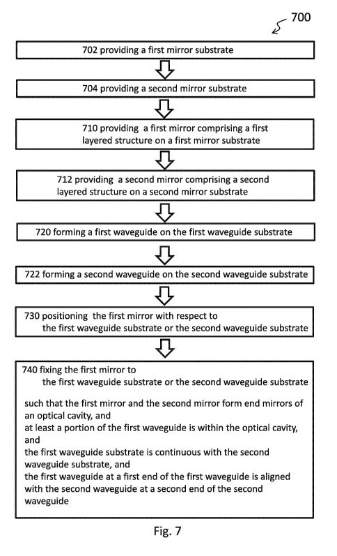
In yet another aspect, the disclosure relates to a method for producing a
photonic integrated
circuit, the method comprising: providing a first waveguide substrate with a
first waveguide,
providing a second waveguide substrate with a second waveguide, providing a
first mirror
17
CA 03190780 2023-02-03
WO 2022/034038
PCT/EP2021/072193
comprising a first layered structure on a first mirror substrate, providing a
second mirror
comprising a second layered structure on a second mirror substrate, forming a
first waveguide
on the first waveguide substrate, forming a second waveguide on the second
waveguide
substrate, characterized in that the method comprises the following steps:
positioning the first
mirror with respect to the first waveguide substrate or the second waveguide
substrate, and
fixing the first mirror to the first waveguide substrate or the second
waveguide substrate, such
that the first mirror and the second mirror form end mirrors of an optical
resonator, and at
least a portion of the first waveguide is within the optical resonator, and
the first waveguide
substrate is continuous with the second waveguide substrate, and the first
waveguide at a first
end of the first waveguide is aligned with the second waveguide at a second
end of the second
waveguide.
The method may comprise all the process steps, but not necessarily in the
given order. At least
some of the process steps may be performed at an earlier or later point in the
method.
According to one embodiment, the method further comprises forming alignment
structures on
the first mirror substrate or the second mirror substrate. In another
embodiment, the method
further comprises forming alignment structures on the first waveguide
substrate or the second
waveguide substrate.
For example, the alignment structures may comprise alignment marks.
Positioning the first
mirror with respect to the first waveguide substrate or the second waveguide
substrate may
comprise aligning the first mirror with respect to the first waveguide
substrate or the second
waveguide substrate according to a visual inspection of the alignment marks.
For example, the alignment structures may comprise alignment slots.
Positioning the first
mirror with respect to the first waveguide substrate or the second waveguide
substrate may
comprise aligning the first mirror with respect to the first waveguide
substrate or the second
waveguide substrate according to at least one mechanical contact point
provided by at least
one alignment slot.
For instance, forming the first waveguide or the second waveguide can be
performed prior to
the positioning and the fixing.
For instance, forming the first waveguide or the second waveguide can be
performed after the
positioning and the fixing. In particular, forming the first waveguide or the
second waveguide
after the positioning and the fixing can improve the precision of the
alignment. In particular,
forming the first waveguide or the second waveguide after the positioning and
the fixing
18
CA 03190780 2023-02-03
WO 2022/034038
PCT/EP2021/072193
eliminates a risk of misalignment of the first waveguide and the second
waveguide during the
positioning and fixing. The improved precision of the alignment may improve
the coupling of
an electromagnetic wave between the first waveguide and the second waveguide.
For example,
an improved coupling improves the efficiency of a device comprising the
photonic integrated
.. circuit. Eliminating the risk of misalignment can improve the reliability
of a production of the
photonic integrated circuit.
The method may comprise polishing a section of the first mirror substrate
and/or the second
mirror substrate to a surface roughness < 5 nm, in particular < 1 nm.
The method may further comprise depositing the first layered structure or the
second layered
structure. For instance, depositing the first layered structure or depositing
the second layered
structure may comprise ion beam sputtering or magnetron sputtering or
molecular beam
deposition or atomic layer deposition. According to one embodiment, depositing
the first
layered structure or depositing the second layered structure comprises
depositing the first
layered structure or depositing the second layered structure on the first
waveguide or on the
second waveguide.
The method may further comprise removing at least a portion of the first
mirror substrate. The
.. method may further comprise removing at least a portion of the second
mirror substrate.
The positioning and fixing may comprise a microassembly step or a robotic pick-
and-place
step. The microassembly step or the robotic pick-and-place step may comprise
picking up the
first mirror with an automated device. The microassembly step or the robotic
pick-and-place
step may comprise positioning the first mirror with respect to the first
waveguide substrate or
the second waveguide substrate, and/or fixing the first mirror to the first
waveguide substrate
or the second waveguide substrate using an automated device. The microassembly
step or the
robotic pick-and-place step may comprise positioning the first mirror with a
precision of no
larger than lo vtm, in particular no larger than 1 vim.
The method may further comprise forming a recess in the first waveguide
substrate or the
second waveguide substrate, and positioning and fixing the first mirror such
that at least a part
of the first mirror is in the recess. Positioning the first mirror such that
at least a part of the
first mirror is in the recess may comprise aligning the first mirror with
respect to a side or an
edge of the recess.
The method may comprise direct bonding the first waveguide substrate and the
second
waveguide substrate. The direct bonding may for example comprise surface
activated bonding,
19
CA 03190780 2023-02-03
WO 2022/034038
PCT/EP2021/072193
plasma activated bonding, adhesive bonding, anodic bonding, eutectic bonding,
glass frit
bonding, thermocompression bonding, or reactive bonding.
The method may further comprise forming an intermediate layer between the
first mirror
substrate and the first waveguide substrate or the second waveguide substrate.
For instance,
the intermediate layer may comprise silicon or silicon oxide.
The first mirror substrate may have a thickness of at least 1 mm, in
particular of at least 10 mm.
The first waveguide substrate or the second waveguide substrate may have a
thickness of at
least 1 mm, in particular of at least lo mm.
The method may further comprise attaching the first waveguide substrate or the
second
waveguide substrate to an auxiliary substrate with a thickness of at least 1
mm, in particular of
at least 10 mm.
A thickness of the first mirror substrate, or the first waveguide substrate,
or the second
waveguide substrate, or the auxiliary substrate of at least 1 mm, in
particular at least 10 mm,
makes handling the respective substrate more reliable. In particular, it
reduces a risk of
unintendedly breaking the respective substrate during the positioning and
fixing. The
thickness of at least 1 mm, in particular of at least 10 mm, also improves the
adhesion between
the first mirror substrate and the first waveguide substrate or the second
waveguide substrate.
The improved adhesion reduces a danger that a joint between the first mirror
substrate and
the first waveguide substrate or the second waveguide substrate breaks, in
particular in the
presence of movements or vibrations. For example, the improved adhesion
improves the
reliability of the production of the photonic integrated circuit. For example,
the improved
adhesion enhances a lifetime of the photonic integrated circuit. Large
thickness substrates
typically also show less bowing and warping, i.e. are flatter, which may be
favorable with
respect to the performance of the device. The thickness of at least 1 mm, in
particular of at least
10 mm, also improves a thermal transport between the first mirror substrate
and the first
waveguide substrate or the second waveguide substrate.
The method may further comprise attaching a heat sink to the first waveguide
substrate or to
the second waveguide substrate. For instance, a thermal conductivity of the
heat sink may be
at least 150 W/(m=K).
The heat sink may comprise diamond, silicon carbide, aluminum nitride, copper,
silver or gold.
CA 03190780 2023-02-03
WO 2022/034038
PCT/EP2021/072193
Attaching the heat sink may comprise depositing diamond or silicon carbide by
chemical vapor
deposition.
The method may further comprise attaching at least two heat sinks to surfaces
on opposite
sides of the first waveguide substrate.
Brief Description of the Drawings
The features and numerous advantages of the disclosure will become best
apparent from a
to detailed description of exemplary embodiments with reference to the
accompanying drawings,
in which:
Fig. 1 is a schematic illustration of a top view of the photonic integrated
circuit according to
one embodiment;
Fig. 2 is a schematic illustration of the photonic integrated circuit
according to another
embodiment;
Fig. 3 gives schematic illustrations of a top view of the photonic integrated
circuits with
focusing or defocusing elements according to yet another embodiment;
Fig. 4 illustrates optical devices using an optical parametric oscillator or a
single-photon
source based on the photonic integrated circuit;
Fig. 5 illustrates optical devices using a squeezed-light source based on the
photonic
integrated circuit;
Fig. 6 is a schematic illustration of a cross sectional side view of the
photonic integrated
circuit, further comprising a heat sink according to an embodiment;
Fig. 7 gives a process flow illustrating a method for producing the photonic
integrated circuit;
Fig. 8 illustrates a method for producing the photonic integrated circuit
according to an
embodiment;
Fig. 9 illustrates a method for producing the photonic integrated circuit
according to another
embodiment
21
CA 03190780 2023-02-03
WO 2022/034038
PCT/EP2021/072193
Fig. 10 illustrates a method for producing the photonic integrated circuit
comprising a
microassembly step or a robotic pick-and-place step;
Fig. 11 illustrates a method for producing the photonic integrated circuit
comprising a direct
bonding step.
Detailed Description
Fig. 1 gives a schematic illustration of a photonic integrated circuit loo
according to one
embodiment, which may, for example, be applied as an optical parametric
oscillator 460, a
cavity-enhanced photon-pair source 462, or a cavity-enhanced source of
squeezed light 56o.
The photonic integrated circuit is shown from a top view. In this embodiment,
a first
mirror 120 and a second mirror 120 are located on opposite surfaces of a first
waveguide
substrate 104, which thus serves as a first mirror substrate 124 and a second
mirror
substrate 134. According to this embodiment, the first waveguide 102 is fully
within the optical
resonator formed by the two mirrors 120, 130. The first waveguide substrate
104 comprises a
nonlinear medium 140, for example lithium niobate, with a portion of the
nonlinear medium
configured as a nonlinear gain medium, for example by periodic poling to form
a section of
periodically poled lithium niobate. For example, the first waveguide substrate
104 can be a
single crystal of lithium niobate. The lithium niobate may comprise titanium-
indiffused
lithium niobate. The electric field of an incoming electromagnetic wave 152,
which can
advantageously be generated in a photonic integrated circuit loo according to
a slightly
modified embodiment adapted for second-harmonic generation, is enhanced in the
optical
resonator. Consequently, the electric field is enhanced in the first waveguide
102, 106 formed
in the nonlinear medium. The enhanced field strength enhances the efficiency
of a device
comprising the nonlinear medium. Advantageously, the periodic poling of the
lithium
niobate 140 may be optimized for a specific nonlinear optical process to occur
at a specified
temperature for a specific incoming frequency and incoming polarization. For
example, the
periodicity can be adapted to support degenerate parametric down conversion
for an incoming
frequency corresponding to an incoming wavelength of 775 nm. In this case, a
seeded or
unseeded degenerate parametric downconversion results in an electromagnetic
wave 154 with
a frequency corresponding to a wavelength of 1550 nm. The photonic integrated
circuit loo
can generate an electromagnetic wave 154 that comprises squeezed light, or
generate photon
pairs. The generated electromagnetic wave 154 may pass through the nonlinear
optical
medium more than once because of the optical resonator formed by the first
mirror 120 and
22
CA 03190780 2023-02-03
WO 2022/034038
PCT/EP2021/072193
the second mirror 130. Multiple passes of the generated light can be used to
seed the nonlinear
optical process, which can enhance an output power of the nonlinear optical
process, and to
implement a device which is referred to as an optical parametric oscillator in
the context of this
disclosure. The multiple passes can hence be beneficial for the efficiency of
a device adapted to
support the nonlinear optical process. In particular, the photonic integrated
circuit may be
applied as a source of intense squeezed light. The multiple passes and the
enhanced field
strength in the optical resonator can improve the performance of an optical
device comprising
the photonic integrated circuit, in particular of a source of squeezed light,
for example by
relaxing the demands on a possible source of optical or electric power which
may be needed to
operate the optical device. For example, the cost of the source may hence be
reduced. An output
power of the optical device can be improved. A quality of a squeezing of
generated squeezed
light can be improved. The improved efficiency of the device also reduces
waste heat generated
in the device, which may be beneficial for a stability of the generated light
and a lifetime of the
device.
Fig. 2 gives a schematic perspective view of a different embodiment of the
photonic integrated
circuit 200 for, for example, an optical parametric oscillator 460, a cavity-
enhanced photon-
pair source 462, or a cavity-enhanced source of squeezed light 56o. Like in
the embodiment
illustrated in Fig. 1, also according to the embodiment depicted in Fig. 2 the
first mirror 120,
220 and the second mirror 130, 230 form end mirrors of an optical resonator.
Like in the other
embodiment, a portion 206 of the first waveguide is in the optical resonator.
In addition, this
embodiment of the photonic integrated circuit 200 can be adapted to support a
nonlinear
optical process, giving the same advantages as the photonic integrated circuit
shown in Fig. 1.
According to the embodiment shown in Fig. 2, the first mirror substrate 224 is
fixed to the first
waveguide substrate 204, and the second mirror 230 is fixed to one of the
waveguide
substrates 204, 214. In some embodiments, the first mirror substrate 124, 224
is provided by
one of the waveguide substrates, whereas the second mirror substrate 234 is
fixed to one of the
waveguide substrates. In some embodiments, the first mirror 120, 220 and the
second
mirror 130, 230 are formed on the same mirror substrate, the same mirror
substrate acting as
the first mirror substrate 124, 224 and the second mirror substrate 134, 234.
In this case, the
first mirror 120, 220 and the second mirror 130, 230 can be formed on opposite
surfaces of the
same substrate. This same substrate can then be fixed to the first waveguide
substrate 104, 204
or the second waveguide substrate 114, 214.
The photonic integrated circuit loo may comprise a second waveguide substrate
114 of a
material different from the material of the first waveguide substrate 104,
thus implementing a
hybrid approach to photonic integrated circuits. The hybrid approach has the
advantage that
the most suitable material of the second waveguide substrate 114 can be
selected for a target
23
CA 03190780 2023-02-03
WO 2022/034038
PCT/EP2021/072193
functionality of the optical components on the second waveguide substrate 114,
which can be
different from a target functionality of the optical components on the first
waveguide
substrate 104. This allows for the design of complex photonic integrated
circuits. For example,
microstructures, waveguides, ring resonators, phase shifters interferometers,
beam splitters,
delay lines, heat sinks and electronic elements can be on the first waveguide
substrate 104 or
the second waveguide substrate 114 whichever has a more suitable material for
the component.
Additional waveguides and ring resonators are shown in the photonic integrated
circuit wo in
Fig. 1 as examples. An additional third waveguide substrate or more waveguide
substrates,
possibly comprising a third or more different materials, can be continuous
with the first
waveguide substrate 104 or the second waveguide substrate 114, forming a
single chip. The
chip can combine multiple materials, wherein each one may be best-suited for a
specific
functionality.
According to the embodiment shown in Fig. 1, the second layered structure 132
of the second
mirror 130 is fully enclosed in a continuous chip formed by the first
waveguide substrate 104
and the second waveguide substrate 114. This embodiment may result in an
efficient optical
coupling between the first waveguide and the second waveguide, as it minimizes
the optical
losses, for example scattering losses, associated with the optical coupling.
The efficient optical
coupling can improve the quality of the squeezing of a squeezed light, which
can be generated
in a portion of the first waveguide. The efficient coupling is also beneficial
for a high finesse of
the optical resonator, which can be an advantage in some applications. The
continuous chip
may also result in a high heat conduction between the second mirror 120 and
the first
waveguide substrate 104 and the second waveguide substrate 114. The first
mirror 120 and the
second mirror 130 are in physical contact with the nonlinear medium for a high
heat
conduction also between the nonlinear medium and the mirrors 120, 130. The
efficient
transport of heat away from the nonlinear medium and the first mirror 120 and
the second
mirror 130 into the first waveguide substrate 104 and the second waveguide
substrate 114 may
be an advantage in applications which require a high thermal stability and
homogeneity. For
example, this may be the case in the generation of squeezed light with a high
intensity of the
.. pump light. Advantageously, the heat transport away from the first
waveguide substrate 104
and the second waveguide substrate 114 is facilitated by using heat sinks that
are attached close
to or are in contact with the components in which heat originates.
The first waveguide 102, 202 and the second waveguide 112, 212 are aligned
with respect to
each other at corresponding ends. In particular, one end 108, 208 of the first
waveguide
neighbors one end 118, 218 of the second waveguide 112, 212. The alignment is
such that an
extension of an axis of the first waveguide 102, 202 at an end 108, 208 of the
first waveguide
coincides with an axis of the second waveguide 112, 212 at an end 118, 218 of
the second
24
CA 03190780 2023-02-03
WO 2022/034038
PCT/EP2021/072193
waveguide. This way, light can couple directly along a straight line from the
first waveguide
102, 202 to the second waveguide 112, 212. This avoids coupling elements that
would otherwise
be needed for compensating angular misalignment. In some known integrated
photonic
circuits, coupling elements are comprised to compensate an angular
misalignment or to bridge
a significant gap between the axis of the first waveguide 102, 202 and the
axis of the second
waveguide 112, 212 at their corresponding ends or control the divergence of a
light beam.
Avoiding coupling elements reduces optical losses due to scattering and
absorption in the
coupling elements and at interfaces of the coupling element. This improves the
efficiency of
devices comprising the photonic integrated circuit. The reduced optical losses
due to scattering
.. and absorption also increase the finesse of the optical resonator, which is
an advantage in many
devices in which the photonic integrated circuit can be applied. The increased
finesse results
in a higher electric field strength inside the optical resonator and a sharper
resonance profile
of the optical resonator. This is an advantage in narrow-linewidth
applications using the
photonic integrated circuit. Moreover, avoiding the coupling elements reduces
the complexity
.. of producing the photonic integrated circuit, as fewer components are
produced and/or placed
with a high accuracy. Avoiding coupling elements also reduces the cost of
producing the
photonic integrated circuits and improves the reliability of the production.
Moreover, the
mechanical integrity and rigidity is improved, as fewer components can move
with respect to
each other, for example in the presence of a mechanical vibration. For an
efficient coupling,
the end 108, 208 of the first waveguide and the end 118, 218 of the second
waveguide are
located in enclosed vicinity of one another in one embodiment. In particular,
the end 108 of
the first waveguide can be in direct contact with the first mirror 120 or the
second mirror 130,
and the end 118 of the second waveguide can also be in direct contact with the
first mirror 120
or the second mirror 130, thus minimizing the distance in between them to a
minimal distance
.. given by a thickness of the first mirror 120, 220 or the second mirror 130,
230.
Fig. 3 illustrates another embodiment of the photonic integrated circuit,
comprising a focusing
or defocusing element 350 between the first waveguide 102 the second waveguide
112. The
focusing or defocusing element may improve the coupling between the first
waveguide 102,
202 and the second waveguide 112, 212. For example, the embodiments
illustrated in Fig. 3
comprise as a focusing or defocusing element a micro-lens 352, 354 as shown in
Fig. 3A and
Fig. 3B, a micro beam expander 356 as shown in Fig. 3C, or a coupling grating
358 or a GRIN
lens 358 as shown in Fig. 3D. In one embodiment, illustrated in Fig. 3A, the
first mirror 120 or
the second mirror 130 comprises or is the curved mirror 350, 352. This
minimizes the number
.. of optical components in the optical resonator or close to the optical
resonator, which could
act as sources of scattering and/or absorption. In some embodiments, the
curved mirror has a
radius of curvature of loo rn to 300 m. The curved mirror can have any
shape, including
spherical, cylindrical, parabolic, or the shape of a general Cartesian oval.
Parabolic and
CA 03190780 2023-02-03
WO 2022/034038
PCT/EP2021/072193
Cartesian oval shapes may be an advantage as the radius of curvature may not
be much larger
than the diameter of a beam of incoming radiation in an application, provoking
spherical
aberration. The parabolic and Cartesian oval shapes compensate the spherical
aberration. The
focusing or defocusing element can be configured to maximize the stability of
the optical
resonator. Moreover, the focusing or defocusing element can be configured to
maximize the
finesse of the optical resonator. In another embodiment, a space between the
first waveguide
102 or the second waveguide 112 and the first mirror 120 or the second mirror
130 comprises
vacuum or a filler material. The filler material reduces the difference in the
optical index of
refraction at an interface of the first waveguide 102 or the second waveguide
112. This further
improves the coupling between the first waveguide 102 and the second waveguide
112. The first
mirror substrate 124 or the second mirror substrate 134 may further exhibit at
least one layered
structure. The first mirror substrate can for example support an
antireflection coating, an
optical bandpass filter, an optical short pass filter, or an optical long pass
filter. In particular,
the antireflection coating can improve the coupling between the first
waveguide and the second
waveguide, for example by reducing reflection losses of a pump light or a
generated light.
In one embodiment, the first waveguide 102, 202 or the second waveguide 112,
212 comprises
lithium niobate, silicon, silicon oxide, aluminum arsenide, gallium arsenide,
aluminum
gallium arsenide, or silicon nitride, but the first waveguide 102, 202 or the
second
waveguide 112, 212 may be composed of any semiconductor or dielectric that is
now known or
developed in the future. In an embodiment, the first waveguide 102, 202 or the
second
waveguide 112, 212 comprises titanium-indiffused lithium niobate or silicon-
indiffused silicon
oxide. Also, in one embodiment, the first waveguide substrate 104, 204 or the
second
waveguide substrate 114, 214 comprises lithium niobate, silicon, silicon
oxide, aluminum
arsenide, gallium arsenide, aluminum gallium arsenide, or silica nitrite, but
the first waveguide
substrate 104, 204 or the second waveguide substrate 114, 214 may be composed
of any
semiconductor or dielectric that is now known or developed in the future. The
first waveguide
substrate 104, 204 or the second waveguide substrate 114, 214 can comprise
crystalline
material, for example in the form of a wafer.
The first layered structure 122, 222 or the second layered structure 132, 232
each comprise at
least one layer of material different from the first waveguide substrate 104,
204 and the second
waveguide substrate 114, 214. The first layered structure 122, 222 or the
second layered
structure 132, 232 may comprise alternating layers of materials with a low
index of refraction
and materials with a high index of refraction. This combination ensures a high
reflectivity
(>98 %, > 99 %, > 99.5 %, > 99.9 %, or > 99.99 %). A material forming a layer
of the layered
structure may comprise an oxide or a halide or a chalcogenide or a III-V-
semiconductor, for
example TiO2, SiO2, MgF2, Ta205, ZnSe, YF3, AlGaAs, GaAs, AlAs, AlAsSb, or
GaSb. The
26
CA 03190780 2023-02-03
WO 2022/034038
PCT/EP2021/072193
layers may also be composed of any other semiconductor or dielectric that is
now known or
developed in the future. The first layered structure 122, 222 and the second
layered
structure 132, 232 can have thicknesses below 30 vtm, in particular below 20
VIM. The
thicknesses can be at least 1 vtm, in particular at least 5 vim. The first
layered structure 122, 222
or the second layered structure 132, 232 can comprise a metal layer e.g. gold,
silver, or
aluminum coating). A metal layer has the advantage that it can be produced
economically,
while providing a reflectivity > 85 %, > 90 %, or > 95 %. A section of the
mirror substrate can
have a roughness of RMS <5 nm, in particular <1 nm. In particular, this may be
useful for
producing ultra-high performance mirrors (reflectivity exceeding 99.99 %),
while for all other
applications (reflectivity > 98 %,> 99 %,> 99.5 %, or > 99.9 %) industrial
grade polishing can
possibly be employed. A deposited layer may comprise an epitaxial
semiconductor layer,
wherein the material forming the epitaxial layer can be the same or different
from the material
forming the substrate. A first mirror 120, 220 or a second mirror 130, 230
which comprises the
epitaxial layer can have a reflectivity > 99.9 % or > 99.99 %. Mirrors
comprising an epitaxial
semiconductor layer usually comprise a mirror substrate that comprises
crystalline material.
The first layered structure 122, 222 and/or the second layered structure 132,
232 thus achieve
a high reflectivity of the first mirror 120, 220 and the second mirror 130,
230. The high
reflectivity results in a high finesse of the optical resonator. The
combination of a high finesse
and a short length of the optical resonator is an advantage over existing ring
resonators, for
example when the photonic integrated circuit is used for generating single
frequency modes of
ultra-narrow bandwidth or for wavelength-division multiplexing.
Moreover, the reflectivity and transmittance of the first mirror 120, 220
and/or the second
mirror 130, 230 can easily be adjusted according to the requirements of a
specific application
by designing the first layered structure 122, 222 and/or the second layered
structure 132, 232
correspondingly. The first layered structure 122, 222 and/or the second
layered structure 132,
232 can have a transmittance of at least 1 %, in particular at least 25 %, or
at least 40 %. The
transmittance of the first layered structure 122, 222 and/or the second
layered structure 132,
232 can be used to couple the incoming electromagnetic wave into the optical
resonator, or to
couple the generated electromagnetic wave out of the optical resonator.
The reflectivity and transmittance of the first mirror 120, 220 and the
reflectivity and
transmittance of the second mirror 130, 230 can be configured for impedance
matching. In
particular, the reflectivity and transmittance of the first mirror 120, 220
and the reflectivity
and transmittance of the second mirror 130, 230 can be configured such that a
light power
transmitted through the first mirror 120, 220 or the second mirror 130, 230 is
at most as high
as a light power dissipated during a round trip in the optical resonator. The
reflectivity and
27
CA 03190780 2023-02-03
WO 2022/034038
PCT/EP2021/072193
transmittance can be adjusted individually for each frequency of an
electromagnetic wave in
the presence of multiple frequencies of at least one electromagnetic wave, for
example if an
incoming frequency differs from a generated frequency in the device using the
photonic
integrated circuit, or in case of multiple, differing incoming frequencies or
multiple, differing
generated frequencies.
The first mirror substrate 124, 224 or the second mirror substrate 134, 234
can be composed
of materials which are the same or different from the material of the first
waveguide
substrate 104, 204 or the second waveguide substrate 114, 214. In one
embodiment, the first
lo mirror substrate 124, 224 or the second mirror substrate 134, 234
comprises lithium niobate,
silicon, silicon oxide, aluminum arsenide, gallium arsenide, aluminum gallium
arsenide, or
silicon nitride, but the first mirror substrate 124, 224 or the second mirror
substrate 134, 234
may be composed of any semiconductor or dielectric that is now known or
developed in the
future. In one embodiment, a portion of the first layered structure 122 or the
second layered
structure 132 is embedded within a continuous body formed by the first
waveguide
substrate 104 and the second waveguide substrate 114 as illustrated in Fig. 1.
In another
embodiment, the first layered structure 122 or the second layered structure
132 is fully
embedded within the continuous body formed by the first waveguide substrate
104 and the
second waveguide substrate 114 as illustrated in Fig. 1. In another
embodiment, at least a
portion of the first layered structure 222 or the second layered structure 232
is below a top
surface of the first waveguide substrate 204 or the second waveguide substrate
214 as
illustrated in Fig. 2. In an embodiment, the layers of the first layered
structure 122, 222 or the
layers of the second layered structure 132, 232 are perpendicular to a top
surface of the first
waveguide substrate 104, 204 or a top surface of the second waveguide
substrate 114, 214.
The first waveguide 102, 202 can comprise a nonlinear medium. The photonic
integrated
circuit with the nonlinear optical medium has the advantage that the strength
of an
electromagnetic wave in the waveguide is enhanced due to the transverse
confinement in the
waveguide and the confinement along the optical axis in the optical resonator
enhances. The
enhanced strength of the electromagnetic field improves the efficiency of a
device which
comprises the optical resonator, in particular of a device adapted to support
a nonlinear optical
process mediated by the nonlinear optical medium. For example, a required
optical or
electrical input power or pump power is reduced, an amount of generated heat
is reduced, a
generated optical output power is improved, or a squeezing of a generated
light is improved.
The nonlinear medium can for example comprise BBO, LBO, KDP, KTP, KTA, KBBF,
BiBO,
CLBO, KTA, GaAs, AgGaS2, ZnTe, InP, GaSe, CdTe, CdZnTe, LiTa03, or LiNb03. The
nonlinear optical medium can alternatively comprise any nonlinear optical
material that is now
known or developed in the future. The nonlinear optical medium may for example
be adapted
28
CA 03190780 2023-02-03
WO 2022/034038
PCT/EP2021/072193
to support parametric down conversion, second harmonic generation, sum
frequency
generation, difference frequency generation, four-wave mixing, optical
parametric
amplification, optical parametric oscillation, white-light generation, Kerr
lensing, two-photon
absorption, multi-photon absorption, or stimulated amplified emission. In an
embodiment,
the nonlinear optical medium has a non-vanishing Chi2 nonlinearity. This is
realized in
nonlinear optical media without inversion symmetry. In an embodiment, the
nonlinear optical
medium without inversion symmetry is ferroelectric. For example, the nonlinear
optical
medium can comprise lithium niobate, in particular it can comprise titanium-
indiffused
lithium niobate. The lithium niobate can comprise periodically poled lithium
niobate 140.
Periodic poling of the ferroelectric domains in periodically poled lithium
niobate 140 allows
for tuning phase matching conditions of the nonlinear optical medium. By
tuning the phase
matching conditions, the nonlinear optical medium can be configured to support
a specified
nonlinear optical process, or can be configured to support nonlinear optical
processes for
specified frequencies of electromagnetic waves, or can be configured to
support a nonlinear
process at a specified temperature. This flexibility is advantageous in
applications, as it enables
an average expert in the field to design a photonic integrated circuit for a
specific application.
In an embodiment, the nonlinear optical medium is adapted to support a
nonlinear optical
process comprising a frequency conversion. In an embodiment, the frequency
conversion
comprises at least one incoming electromagnetic wave 152 with an incoming
frequency and at
least one generated electromagnetic wave 154 with a generated frequency, and
the generated
frequency is different from the incoming frequency. In one embodiment, the
generated
frequency is smaller than the incoming frequency. For example, this is
achieved by employing
parametric down conversion, optical parametric amplification, optical
parametric oscillation,
or four-wave mixing as a nonlinear optical process. In another embodiment, at
least one
generated frequency is the double of at least one incoming frequency. For
example, this can be
achieved using second harmonic generation in the nonlinear optical medium. The
optical
resonator can be configured to enhance a field strength of the incoming
electromagnetic
wave 152 inside the optical resonator compared to a field strength of the
incoming
electromagnetic wave 152 outside the optical resonator. The enhanced field
strength can
advantageously increase the efficiency of a device which comprises the optical
resonator and
is adapted to support the nonlinear optical process. In one embodiment, the
generated
electromagnetic wave 154 passes through the portion 106, 206 of the first
waveguide inside the
optical resonator more than once, realizing a multi-pass geometry. In the
multi-pass geometry,
the generated electromagnetic wave 154 can further seed the nonlinear optical
processes. This
increases the efficiency of a device comprising the optical resonator further.
The increased
efficiency improves the performance of the device for example by relaxing the
requirements
with respect to a source of optical or electrical pump power, thereby reducing
the technical
29
CA 03190780 2023-02-03
WO 2022/034038
PCT/EP2021/072193
requirements towards the device and its cost. The increased efficiency also
improves the
squeezing of squeezed light which can be generated in the nonlinear optical
process.
The incoming frequency of the incoming electromagnetic wave 152 can be in the
UV, or the
visible, or the infrared spectral range, with a wavelength of at least 200 nm,
in particular
400 nm. The wavelength may be at most 10 vtm, in particular at most 1600 nm.
Depending on
the specific incoming frequency or frequencies, and depending on the generated
frequency or
frequencies, specific materials of the first waveguide 102, 202 or the second
waveguide 112, 212
may need to be employed. In particular, the material of the first waveguide
102, 202 and the
second waveguide 112, 212 should exhibit a high transparency to the incoming
frequency or
the generated frequency. The photonic integrated circuit advantageously
provides the
flexibility to employ a wide selection of materials such that the wavelength
range may be
tailored to a specific application. In particular, the incoming frequency can
be in the
wavelength range from 840 to 860 nm, from 1300 to 1320 nm, from 1370 to 1390
m, or from
1540 to 156o nm. Advantageously, an incoming electromagnetic wave 152 of such
a wavelength
is transported efficiently in commonly used optical fibers. Using such an
incoming frequency
allows to integrate the photonic integrated circuit into extended optical
devices. In one
embodiment, the incoming frequency can be in the wavelength range from 420 to
430 nm,
from 65o to 660 nm, from 685 to 695 nm, or from 770 to 780 nm, in particular
in the
wavelength range from 770 to 780 nm. Using such an incoming frequency in
combination with
degenerate parametric down conversion results in generated frequencies, which
can
advantageously be transmitted with low loss in commonly used optical fibers.
In another
embodiment, the incoming frequency can be in the wavelength range from 1640 to
1680 nm,
from 1680 to 1720 nm, from 2600 to 2640 nm, or from 3080 to 3120 nm, in
particular in the
wavelength range from 3080 to 3120 nm. Using such an incoming frequency in
combination
with frequency-doubling or second-harmonic generation results in generated
frequencies,
which can advantageously be transmitted with low loss in commonly used optical
fibers.
The generated frequency of the generated electromagnetic wave 154 can be in
the UV, or the
visible, or the infrared spectral range, with a generated wavelength of at
least 200 nm, in
particular 400 nm. The generated wavelength may be at most 10 vtm, in
particular at most
1600 nm. In particular, the generated frequency can correspond to a wavelength
range from
840 to 860 nm, from 1300 to 1320 nm, from 1370 to 1390 m, or from 1540 to
1.56o nm.
Advantageously, a generated electromagnetic wave 154 of such an outgoing
frequency is
transported efficiently and commonly used optical fibers. Using such an
outgoing frequency
allows to integrate the photonic integrated circuit into extended optical
devices, for example
for providing the incoming electromagnetic wave 152 or for processing the
generated
CA 03190780 2023-02-03
WO 2022/034038
PCT/EP2021/072193
electromagnetic wave 154. In an embodiment, the generated wavelength is
between 1540 and
1560 nm.
In one embodiment, the generated electromagnetic wave 154 comprises
electromagnetic wave
in a squeezed state. The combined confinement along the transverse direction
by the
waveguide 106, 206 comprising a nonlinear optical medium and along the optical
axes by the
optical resonator 120, 220, 130, 230 enhances the field strength of an
incoming
electromagnetic wave 152 and improves the quality of the squeezing. Moreover,
the continuous
first waveguide substrate 104, 204 and second waveguide substrate 114, 214
provide a
mechanically robust and rugged platform for squeezed light generation and for
coupling
squeezed light between the different components of an optical device, in
particular a photonic
integrated circuit. Moreover, the first mirror 120, 220 and the second mirror
130, 230
comprising at least one layer of material different from a material of the
first waveguide
substrate 104, 204 and the second waveguide substrate 114, 214 allow for a
high finesse of the
optical resonator, further improving the quality of the squeezing. The
photonic integrated
circuit can hence be applied for the generation of high quality or high
intensity squeezed light,
giving advantages in applications such as squeezed-state encoding 570, quantum
key
distribution 572, quantum computing 574, or wavelength-division multiplexing.
Some
exemplary applications that the photonic integrated circuit can advantageously
be applied in
are illustrated in Fig. 5.
According to the embodiments shown in Fig. 1 and Fig. 2, the first waveguide
is completely
inside the optical resonator formed by the first mirror 120, 220 and the
second mirror 130,
230. According to the embodiment shown in Fig. 1, the length of the optical
resonator matches
the length of the first waveguide. The first layered structure 122, 222 and/or
the second layered
structure can be in physical contact with the first waveguide 102, 202 to
minimize the length
of the optical resonator. This can be achieved by depositing the first layered
structure 122, 222
or the second layered structure 132, 232 directly onto the first waveguide
102, 202. According
to the embodiment shown in Fig. 2, a gap may exist between the first mirror or
the second
mirror and the first waveguide, such that the length of the optical resonator
slightly exceeds
the length of the first waveguide. In some embodiments, the length of the
optical resonator
does not exceed the length of the portion 106, 206 of the first waveguide
inside the optical
resonator by a factor of 10, in particular of 3, or 1.5. According to some
embodiments, the
length of the optical resonator may not exceed 1 m, or loo mm, or 50 mm, or 20
mm. A longer
optical resonator provides better selectivity. A short length of the optical
resonator results in a
compact design with the advantage of reducing optical loss. As an additional
advantage, an
optical resonator with a short length emits a frequency comb with a large
spectral spacing. The
large spectral spacing allows for selecting a single frequency, for example
using bandpass
31
CA 03190780 2023-02-03
WO 2022/034038
PCT/EP2021/072193
filtering or frequency selective homodyne detection. In one embodiment, the
photonic
integrated circuit comprises an optical bandpass filter, or an optical short
pass filter, or an
optical long pass filter located between the first waveguide 102, 202 and the
second waveguide
112, 212. By selecting a single frequency from the frequency comb using the
bandpass filter, an
ultra-narrow bandwidth can be achieved, which is an advantage in some
applications. A large
spectral spacing also allows for wavelength-division multiplexing of the
frequency modes into
individual spatial modes for separate processing of the individual spatial
modes. Therefore,
the first waveguide substrate 104, 204 or the second waveguide substrate 114,
214 can comprise
an array of waveguides or a phase array, which can be adapted to serve as a
monochromator
or a spectroscope. On the other hand, a larger length of the optical resonator
can enhance the
interaction length of a process related to an interaction between light and
matter in the optical
resonator. An enhanced interaction length can enhance the efficiency of a
device which
comprises the optical resonator and is adapted to support the process, which
can for example
comprise the generation of light during the interaction. A short length of the
optical resonator
can be used, for example if the photonic integrated circuit is used in
combination with a pulsed
light source. A short length of the optical resonator reduces the dispersion
inside the optical
resonator and can improve a pulse duration of a generated light pulse.
Atypical width of the first waveguide 102, 202 or the second waveguide 112,
212 may be at least
10 nm, in particular 500 nm, or 1 m, or 2 pm. In one embodiment, the width of
the first
waveguide 102, 202 or the second waveguide 112, 212 does not exceed 1 mm, in
particular
300 m, or 50 vim, or 10 vim, or 8 m. This width is optimized for
applications with
electromagnetic radiation in the ultraviolet, the visible and the infrared
spectral range.
Different widths are possible, optimized for the application and the
wavelength range used. A
tapered shape of the first waveguide 102, 202 or the second waveguide 112, 212
is possible, for
example to improve the coupling between the first waveguide 102, 202 and the
second
waveguide 112, 212. A part of the first waveguide 102, 202 may be embedded in
the first
waveguide substrate 104, 204. A part of the first waveguide 102, 202 may
protrude from the
first waveguide substrate 104, 204. A part of the second waveguide 112, 212
may be embedded
in the second waveguide substrate 114, 214. A part of the second waveguide
102, 202 may
protrude from the second waveguide substrate 114, 214.
The first waveguide 102, 202 and the first waveguide substrate 104, 204 may
form one integral
piece. Also the second waveguide 112, 212 and the second waveguide substrate
114, 214 may
form one integral piece. In a monolithic approach, illustrated in Fig. 2, the
first waveguide
substrate 204 and the second waveguide substrate 114, 214 form an integral
piece. This
approach optimizes the mechanical rigidity of the photonic integrated circuit
and hence its
resilience to unintended movements such as vibrations. The monolithic approach
also ensures
that the first waveguide substrate 204 and the second waveguide substrate 114,
214 can be
32
CA 03190780 2023-02-03
WO 2022/034038
PCT/EP2021/072193
processed together using the same processing techniques. This facilitates the
fabrication of the
photonic integrated circuit and reduces its cost. The monolithic approach can
also be used to
ensure the alignment of the first waveguide 102, 202 and the second waveguide
112, 212, by
initially producing both of them as a continuous waveguide and at a later step
separating them
by a recess in the waveguide.
In another embodiment, consistent with the schematic illustration in Fig. 1,
the first waveguide
substrate 104 and the second waveguide substrate 114 are fixed to one another.
In this case,
the first waveguide substrate 104 and the second waveguide substrate 114 can
be composed of
different materials, consistent with a hybrid approach to photonic integrated
circuits. In the
hybrid approach, the best materials for specific functionalities can be
combined. This may be
an advantage in some applications, as it allows for combining various
functionalities on a single
chip using optimized materials for each of the functionalities. More than two
materials can be
combined into one photonic integrated circuit. This may be an advantage if
more than two
functionalities are to be combined in the photonic integrated circuit.
A thickness of the first waveguide substrate 104, 204 or the second waveguide
substrate 114,
214 may exceed 1 mm, in particular 10 mm. A larger thickness makes the
production process
more reliable, as it reduces the risk of an unintended breaking of the first
waveguide substrate
104, 204 or the second waveguide substrate 114, 214 in the production process.
A larger
thickness also improves the adhesion of the first waveguide substrate 104, 204
to the second
waveguide substrate 114, 214 in embodiments in which the first waveguide
substrate 104, 204
is fixed to the second waveguide substrate 114, 214. The improved adhesion
improves the
rigidity and ruggedness of the photonic integrated circuit in the presence of
mechanical
vibrations. This enhances the lifetime of the photonic integrated circuit.
Large thickness
substrates typically also show less bowing and warping, i.e. are flatter,
which may be favorable
with respect to the performance of the device. This also improves the heat
dissipation within
the photonic integrated circuit. A small thickness is possible if material is
to be saved and the
production cost is to be reduced. In particular, the thickness can be reduced
in embodiments
where the first mirror 120, 220 or the second mirror 130, 230 is fixed to the
first waveguide
substrate 104, 204 or the second waveguide substrate 114, 214, as illustrated
in Fig. 2.
A width of the first waveguide substrate 104, 204 or the second waveguide
substrate 114, 214
may exceed 1 mm, in particular 10 mm. In some embodiments, a length and a
width of the first
waveguide substrate 104, 204 or the second waveguide substrate 114, 214 exceed
1 mm, in
particular 10 mm. A larger width or a large width and length of the first
waveguide substrate
104, 204 or the second waveguide substrate 114, 214 allow for the co-
integration of more
additional components on the photonic integrated circuit, as illustrated for
some example
33
CA 03190780 2023-02-03
WO 2022/034038
PCT/EP2021/072193
optical applications in Fig. 4 and Fig. 5. A smaller width and/or length of
the first waveguide
substrate 104, 204 or the second waveguide substrate 114, 214 is possible if
material is to be
saved to reduce a cost of production of the photonic integrated circuit or to
simplify the co-
integration with electrical, photonic, or micro-electro-mechanical integrated
circuits.
The design of the photonic integrated circuit advantageously permits the
integration of
additional optical resonators, which share with the resonator device, or at
least with a portion
of the resonator device, one chip formed by the continuous first waveguide
substrate 104, 204
and the second waveguide substrate 114, 214. In one embodiment, a third mirror
with a third
lo mirror substrate forms an end mirror of a second optical resonator, and
the third mirror
substrate is provided by or fixed to the chip. In another embodiment, also a
fourth mirror
substrate of a fourth mirror forming an end mirror of the second optical
resonator is provided
by or fixed to the chip. The photonic integrated circuit can comprise a third
waveguide, with at
least a portion of the third waveguide in the second optical resonator. In yet
another
embodiment, the third waveguide is in contact with the chip, so that it is in
contact with the
first waveguide substrate 104, 204 or the second waveguide substrate 114, 214.
A fourth
waveguide can be aligned at a fourth end of the fourth waveguide with the
third waveguide at
a third end of the third waveguide. The integration of multiple optical
resonators in one
photonic integrated circuit is not limited to two optical resonators in a
single photonic
integrated circuit, but a multitude of resonators can in a straightforward way
be integrated in
the same photonic integrated circuit. In an advanced application, tens or
hundreds or
thousands of optical resonators or even more may be integrated in the same
photonic
integrated circuit. In some embodiments, both end mirrors or only one end
mirror of an
additional optical resonator or multiple additional optical resonators are/is
in contact with the
first waveguide substrate 104, 204 or the second waveguide substrate 114, 214.
One
embodiment comprises an additional waveguide at least part of which is located
within an
additional optical resonator. The additional waveguide may comprise an
additional nonlinear
optical medium. The additional nonlinear optical medium may be configured to
support
parametric down conversion, second harmonic generation, sum-frequency
generation,
difference-frequency generation, four-wave mixing, optical parametric
amplification, optical
parametric oscillation, white-light generation, Kerr lensing, two-photon
absorption, or multi-
photon absorption. The waveguide within an additional optical resonator of the
additional
optical resonator can be in contact with the first waveguide substrate 104,
204 or the second
waveguide substrate 114, 214 in one embodiment. Additional waveguides can be
aligned at
their ends with corresponding ends of waveguides which are at least partially
located within
the additional optical resonators.
34
CA 03190780 2023-02-03
WO 2022/034038
PCT/EP2021/072193
Fig. 4 and Fig. 5 illustrate examples of optical devices comprising one or
more photonic
integrated circuits 100, 200. In particular, Fig. 4 shows devices in which the
photonic
integrated circuit 100, 200 serves as or is comprised in an optical parametric
oscillator 460 or
a photon-pair source 462. Fig. 4A and Fig. 4B illustrate devices for frequency-
comb
spectroscopy 470, 472 in particular devices for single-comb spectroscopy 470
or dual-comb
spectroscopy 472. Accordingly, a photonic chip 470 comprises one optical
parametric
oscillator 460 with at least one photonic integrated circuit 100, 200, or two
optical parametric
oscillators 460 with at least two photonic integrated circuits 100, 200. In
case of two or more
optical parametric oscillators, a multiplexer 492 combines the generated light
from the two
optical parametric oscillators. Waveguides 480 are used to guide the light on
the chip. The light
then passes through a sample 464 that the spectroscopy is performed on and is
detected in a
detector 490. The detectors 490 may perform a homodyne detection. All
detectors 490 may be
co-integrated on the same chip as the photonic integrated circuit, or the
detectors 490 may all
be separate from the chip 470, 472 with the photonic integrated circuit as
shown in Fig. 4A or
4B, or at least one of the detectors 490 may be co-integrated while at least
one of the
detectors 490 is separate from the chip 470, 472. The sample 464 may comprise
a gas cell. The
sample 464 may be on the same chip 470, 472 as the photonic integrated
circuit, or the
sample 464 may be separate from the chip as shown in Fig. 4A or 4B. The sample
464 or at
least a portion of the sample 464 may be inside of a signal-enhancing optical
resonator. The
signal-enhancing optical resonator allows for multiple passes of an
electromagnetic wave
through the sample 464. The signal-enhancing resonator may be or comprise a
photonic
integrated circuit according to Claim 1.
Fig. 4C and Fig. 4D show a device in which the photonic integrated circuit
100, 200 serves as
or is comprised in a photon-pair source 462. In particular, Fig. 4C
illustrates a device for
quantum-key distribution 474. The generated light from the photon-pair source
462 passes
through a demultiplexer 494, and one portion of the light is detected on a
reference
photodetector 490. The other portion is sent, possibly after passing through a
phase
shifter 482 and a polarization controller 496, into a channel 466 for
distribution. It is finally
detected by a receiver 468 at another end of the channel.
Fig. 4D illustrates a device for quantum computing with photon pairs. A
photonic chip 476
comprises several photon-pair sources 462, each being or comprising a photonic
integrated
circuit 100, 200. After passing a demultiplexer 494, the photon pairs are
combined in a
network of phase shifters 482 and beam splitters 484 to finally reach
detectors 490.
Fig. 5 illustrates optical devices in which the photonic integrated circuit
100, 200 acts as or is
integrated in a squeezed-light source 56o. For example, in a device for
squeezed-light
CA 03190780 2023-02-03
WO 2022/034038
PCT/EP2021/072193
encoding 570, the generated electromagnetic wave passes through an adjustable
phase shifter
582 and an optical I/Q modulator 598 before it is sent into a channel 566 for
communication,
where it is detected by a receiver 568 at another end of the channel.
Waveguides 58o are used
to guide the light on the chip. Fig. 5B illustrates an optical device for
quantum key distribution,
comprising two squeezed-light sources 56o on a single photonic chip 572, each
squeezed-light
source comprising or being a photonic integrated circuit 100, 200. A first
electromagnetic wave
generated in the first squeezed-light source passes a phase shifter 582 and a
second
electromagnetic wave generated in the second squeezed-light source passes
another phase
shifter 582 before they are combined at a beam splitter 584. An output beam of
the beam
splitter 584 is detected at a photodiode 590, whereas another output beam of
the beam
splitter 584 is coupled into a channel 566 for communication, where it is
finally detected by a
receiver 568 at another end of the channel. Fig. 5C illustrates an optical
device for quantum
computing with squeezed light 574. Similar to the device for quantum computing
with photon
pairs 476, the device 574 comprises several photonic integrated circuits 100,
200 serving as
light sources, in this case as squeezed-light sources 56o, and the generated
electromagnetic
waves are coupled into a network comprising phase shifters 582, beam splitters
584, and delay
lines 586, basically acting as interferometers 588. An output state is probed
at detectors 590.
The optical devices illustrated in Fig. 4 and Fig. 5 are only examples of
optical devices that the
photonic integrated circuit can be advantageously applied in, and the
comprised components
are only examples of components that can be combined on a photonic chip or in
a photon
integrated circuit together with the photonic integrated circuit according to
Claim 1. For
example, at least one of the following can be co-integrated: a sensor, a
Peltier element, or a
heat sink. Co-integration of any other optical, electrical, or micro-electro-
mechanical system
component is possible.
As illustrated for one embodiment in Fig. 6, the photonic integrated circuit
may further
comprise one or several heat sinks 640 in contact with the first waveguide
substrate 604 or the
second waveguide substrate 614. Fig. 6 shows a cross-sectional side view of an
embodiment of
the photonic integrated circuit with heat sinks 640 on both sides of a chip
604, 614 formed by
the continuous first waveguide substrate 604 and second waveguide substrate
614. In some
embodiments, the photonic integrated circuit can have only one heat sink 640
on one side of
the chip 604, 614. In particular, the heat sink 640 may be at a bottom side of
the chip, whereas
the first waveguide 102, 202 and the second waveguide 112, 212 are on a top
side of the chip.
The design of the photonic integrated circuit with the first waveguide and
second waveguide
aligned allows for a large contact area between the heat sink 640 and the
photonic integrated
circuit 604, 614. This is an advantage in devices comprising the photonic
integrated circuits,
in particular in devices in which a stable temperature is critical. In
particular, a strong
requirement in terms of temperature stability of known sources of squeezed
light, for example
36
CA 03190780 2023-02-03
WO 2022/034038
PCT/EP2021/072193
for squeezed state encoding 570, quantum key distribution 572, or quantum
computing 574,
are fulfilled by the photonic integrated circuit. In one embodiment, the
thermal conductivity
of the heat sink 640 exceeds 150 W/(m=K). In one embodiment, the heat sink 640
comprises
diamond, or silicon carbide, or aluminum nitride, copper, silver or gold. In
some embodiments,
the heat sink 640 comprises diamond grown by chemical vapor deposition (CVD)
or silicon
carbide grown by CVD.
Fig. 7 illustrates a method 700 for producing a photonic integrated circuit.
The method
comprises providing 702 a first waveguide substrate 104, 204 and providing 704
a second
waveguide substrate 114, 214. The method further comprises providing 710 a
first mirror 120,
220 comprising a first layered structure 122, 222 on a first mirror substrate
124, 224, as well
as providing 712 a second mirror 130, 230 comprising a second layered
structure 132, 232 on
a second mirror substrate 134, 234. The method further comprises forming 720 a
first
waveguide 102, 202 on the first waveguide substrate 104, 204, and forming 722
a second
waveguide 112, 212 on the second waveguide substrate 114, 214. The method is
characterized
in that it comprises the following steps: positioning 730 the first mirror
120, 220 with respect
to the first waveguide substrate 104, 204 or the second waveguide substrate
114, 214, and
fixing 740 the first mirror 120, 220 to the first waveguide substrate 104, 204
or to the second
waveguide substrate 114, 214. The positioning 730 and fixing 740 is done such
that the first
mirror 120, 220 and the second mirror 130, 230 form end mirrors of an optical
resonator and
that at least a portion 106, 206 of the first waveguide is within the optical
resonator, and that
the first waveguide substrate 104, 204 is continuous with the second waveguide
substrate 114,
214, and that the first waveguide 102, 202 at a first end 108, 208 of the
first waveguide is
aligned with the second waveguide 112, 212 at a second end 118, 218 of the
second waveguide.
The method may comprise all of these process steps, but not necessarily in the
given order. The
order of at least some of the process steps can be switched easily, without
deviating from the
disclosure.
Fig. 8 and Fig. 9 illustrate embodiments of the method 700 in which the order
of some of the
process steps varies. In particular, forming 820, 822 the first waveguide 102,
202 or the second
waveguide 112, 212 is performed prior to the positioning 830 and the fixing
840 according to
one embodiment of the method 800 for producing the photonic integrated circuit
illustrated
in Fig. 8. In another embodiment of the method 900, Fig. 9, forming 920, 922
the first
waveguide 102, 202 or the second waveguide 112, 212 happens after the
positioning 930 and
the fixing 940. In particular, forming 920, 922 the first waveguide 102, 202
or the second
waveguide 112, 212 after the positioning 930 and the fixing 940 ensures the
alignment of the
first waveguide 102, 202 at the first end 108, 208 and the second waveguide
112, 212 at the
37
CA 03190780 2023-02-03
WO 2022/034038
PCT/EP2021/072193
second end 118, 218. This removes the risk of misalignment during the
positioning step. This
approach has the advantage of making the production more reliable. However,
forming 920,
922 the first waveguide 102, 202 or the second waveguide 112, 212 after the
positioning 930
and fixing 940 may involve processing routines, which can damage the first
layered
structure 122, 222 or the second layered structure 132, 232.
The method may comprise forming alignment structures on the first mirror
substrate 124, 224
or the second mirror substrate 134, 234. These alignment structures may
comprise alignment
marks, which are configured to give an optical indication of the position of
the first mirror
substrate 124, 224 or the second mirror substrate 134, 234. The alignment
structures may also
comprise alignment slots 750 on or in the first mirror substrate 124, 224 or
the second mirror
substrate 134, 234. The positioning 730 can comprise optically aligning the
mirror substrate
with respect to the first waveguide substrate 104, 204 or the second waveguide
substrate 114,
214 using the alignment structures. The positioning 730 can comprise moving
the first mirror
substrate 124, 224 with respect to the first waveguide substrate 104, 204 or
the second
waveguide substrate 114, 214, with the first mirror substrate 124, 224 in
contact with the
alignment slots 750. Alignment marks may be formed on the first waveguide
substrate 104,
204 or the second waveguide substrate 114, 214 in addition to the alignment
structures formed
on the first mirror substrate 124, 224 or the second mirror substrate 134,
234. Positioning the
first mirror with respect to the first waveguide substrate or the second
waveguide substrate
may comprise aligning the first mirror with respect to the first waveguide
substrate or the
second waveguide substrate according to at least one mechanical contact point
provided by at
least one alignment slot.
The method may further comprise polishing the first mirror substrate 124, 224
or the second
mirror substrate 134, 234. In particular, the polishing step may comprise
super polishing. The
polishing step may involve polishing a section of the mirror substrates to a
roughness of RMS
<5 nm, in particular < 1 nm. This may be useful for ultra-performance mirrors
(reflectivity
exceeding 99.99 %), while for all other applications industrial grade
polishing (>98 %,
> 99.5 %, or > 99.9 %) could be sufficient.
The method can further comprise depositing the first layered structure 122,
222 or the second
layered structure 132, 232. The depositing may comprise evaporative deposition
or sputter-
deposition or ion-beam sputtering or magnetron sputtering. In one embodiment,
at least one
layer of the first layered structure 122, 222 or the second layered structure
132,232 is produced
using molecular beam deposition or molecular beam epitaxy (MBE). MBE results
in the
formation of at least one epitaxial layer, wherein the material forming the
epitaxial layer can
be the same or different from the material forming the substrate. If
depositing the first layered
38
CA 03190780 2023-02-03
WO 2022/034038
PCT/EP2021/072193
structure 122, 222 or the second layered structure 132, 232 comprises
molecular beam epitaxy,
the layered structure is usually grown on a mirror substrate, which comprises
crystalline
material. In yet another embodiment, a layer of the layered structure of the
mirror is deposited
using atomic layer deposition. The production may further comprise removing at
least a
portion of the first mirror substrate 124, 224 or the second mirror substrate
134, 234 in a
production step after fixing 740 the first mirror 120, 220 to the first
waveguide substrate 104,
204 or the second waveguide substrate 114, 214. Depositing the first layered
structure 122, 222
or depositing the second layered structure 132, 232 may comprise depositing a
layer of the first
layered structure 122, 222 or the second layered structure 132, 232 on the
first waveguide 102,
202 or the second waveguide 112, 212.
Fig. 10 illustrates an embodiment of the method noo, wherein the positioning
1030 and
fixing 1040 of the first mirror 120, 220 comprises a microassembly step or a
robotic pick-and-
place step 1002. The microassembly step or robotic pick-and-place step 1002
comprises
picking up the first mirror substrate 124, 224 by an automated device and
placing it with a
precision better than 10 vtm, in particular better than 1 vim. Prior to the
positioning 730, 1030
and fixing 740, 1040 a recess may be formed 750 in the first waveguide
substrate 104, 204 or
the second waveguide substrate 114, 214, such that at least a part of the
first mirror 120, 220 is
in the recess after the positioning 730 and fixing 740.
Fig. 11 illustrates an embodiment of the method 700, wherein the positioning
730 and
fixing 740 comprise direct bonding noo the first waveguide substrate 104 and
the second
waveguide substrate 114 The direct bonding may for example comprise surface
activated
bonding, plasma activated bonding, adhesive bonding, anodic bonding, eutectic
bonding, glass
frit bonding, thermocompression bonding, or reactive bonding. The direct
bonding can, for
example, comprise a chemical cleaning step using a solvent 1160 as illustrated
in Fig. nA. The
direct bonding can, for example, comprise a treatment with a plasma 1170 as
illustrated in
Fig. 11B. The direct bonding can, for example, comprise a direct bonding of
the first mirror 120
and the first waveguide substrate 104 or the second waveguide substrate 114 in
a vacuum
apparatus 1180 as illustrated in Fig. 11C. An intermediate layer may be formed
between the
first mirror 120 and the first waveguide substrate 104 or the second waveguide
substrate 114.
The intermediate layer can comprise silicon or silicon oxide.
The first mirror substrate 124, 224 can have a thickness of at least 1 mm, in
particular of at
.. least 10 mm. The first waveguide substrate 104, 204 or the second waveguide
substrate 114,
214 can have a thickness of at least 1 mm, in particular of at least 10 mm.
Also, the first
waveguide substrate 104, 204 or the second waveguide substrate 114, 214 can be
attached to
an auxiliary substrate with a thickness of at least 1 mm, in particular of at
least 10 mm. A
39
CA 03190780 2023-02-03
WO 2022/034038
PCT/EP2021/072193
sufficient thickness of the first mirror substrate 124, 224 or the first
waveguide substrate 104,
204 or the second waveguide substrate 114, 214 or the auxiliary substrate
advantageously
makes handling the substrate more reliable and avoids breaking a substrate
during the
positioning 730 and fixing 740. It also improves an adhesion between the first
mirror 120, 220
and the first waveguide substrate 104, 204 or the second waveguide substrate
114, 214, making
a joint more reliable, and reducing the danger that the joint breaks in the
presence of
movements and vibrations.
Producing the photonic integrated circuit can further comprise attaching a
heat sink 640 as
lo illustrated in Fig. 6 to the first waveguide substrate 104, 204, 604 or
to the second waveguide
substrate 114, 214, 614. The heat sink 640 allows for an efficient thermal
management of the
photonic integrated circuit. The heat sink 640 can comprise diamond, silicon
carbide,
aluminum nitride, copper, silver or gold. Forming the heat sink may comprise
chemical vapor
deposition of diamond or silicon carbide. The design of the photonic
integrated circuit
advantageously allows for at least two heat sinks 640 on different sides of
the first waveguide
substrate or the second waveguide substrate 604, 614 as illustrated in Fig. 6.
The description and the drawings are intended to illustrate the disclosure and
the numerous
advantages associated therewith, but should not be understood to imply any
limitation. The
scope of the disclosure is to be determined from the appended claims.