Note: Descriptions are shown in the official language in which they were submitted.
WO 2022/051593
PCT/US2021/049017
BUILDING INTEGRATED PHOTOVOLTAIC SYSTEM
Cross-Reference to Related Application
This application relates to and claims the benefit of commonly-owned, co-
pending U.S.
Provisional Patent Application Serial No. 63/074,268, filed September 3, 2020,
entitled
"PHOTOVOLTAIC SHINGLES AND METHODS OF INSTALLING SAME," the contents of
which is incorporated herein by reference in its entirety.
Field of the Invention
The present invention relates to a building integrated photovoltaic system.
Background of the Invention
Photovoltaic systems having solar panels are commonly installed on roofing of
structures.
What is needed is a building integrated photovoltaic system configured to be
efficiently installed
on a roof structure.
Summary of the Invention
In some embodiments, a system, includes a plurality of photovoltaic modules
installed on
a roof deck, wherein the photovoltaic modules are arranged in an array on the
roof deck, wherein
each of the photovoltaic modules includes a first end and a second end
opposite the first end, at
least one solar cell, a first encapsulant encapsulating the at least one solar
cell, wherein the first
encapsulant includes a first surface and a second surface opposite the first
surface, a frontsheet
juxtaposed with the first surface of the first encapsulant, wherein the
frontsheet includes a glass
1
CA 03191420 2023- 3- 1
WO 2022/051593
PCT/US2021/049017
layer, a second encapsulant, and a first polymer layer, a backsheet juxtaposed
with the second
surface of the encapsulant, wherein the backsheet includes a first layer, and
a second polymer layer
attached to the first layer, wherein the first layer forms a lower surface of
the photovoltaic module,
and a wire cover bracket located at the first end, wherein the wire cover
bracket of one of the
photovoltaic modules is configured to overlap the wire cover bracket of an
adjacent another one
of the photovoltaic modules, and wherein the wire cover bracket is configured
to receive at least
one electrical component.
In some embodiments, the first encapsulant is selected from the group
consisting of
thermosetting polyolefin, thermosetting polyolefin encapsulant material,
thermosetting ethylene-
vinyl acetate (EVA), EVA encapsulants, thermoplastic olefin, thermoplastic
polyolefin (TPO) and
hybrids and combinations thereof. In some embodiments, the first encapsulant
includes a
thermosetting polyolefin encapsulant material. In some embodiments, the first
encapsulant has a
thickness of 1 nm to 900 him.
In some embodiments, the first polymer layer includes a fluoropolymer. In some
embodiments, the fluoropolymer is selected from the group consisting of
ethylene
tetrafluoroethylene (ETFE), polyvinylidene fluoride (PVDF),
tetrafluoroethylene-
hexafluoropropyl en e copolymers (F EP), tetrafluoroethyl en e-h
exafluoropropyl ene-vinyli den e
fluoride copolymers (THV), polyvinyl fluoride (PVF), and blends thereof. In
some embodiments,
the first polymer layer includes a material selected from the group consisting
of acrylics,
polyesters, silicones, and polycarbonates. In some embodiments, the first
polymer layer has a
thickness of 0.01 mm to 0.5 mm. In some embodiments, the first layer includes
a polymer. In
some embodiments, the first layer includes thermoplastic polyolefin (TPO).
In some
2
CA 03191420 2023- 3- 1
WO 2022/051593
PCT/US2021/049017
embodiments, the first layer includes polyvinyl chloride (PVC). In some
embodiments, the first
layer includes ethylene propylene di ene monomer (EPDM) rubber.
In some embodiments, the system further includes at least one jumper module
electrically
connecting a first subarray of the array and a second subarray of the array,
wherein the at least one
jumper module includes, at least one electrical bussing, an encapsulant
encapsulating the at least
one electrical bussing, wherein the encapsulant of the at least one jumper
module includes a first
surface and a second surface opposite the first surface of the encapsulant of
the at least one jumper
module, wherein the at least one electrical bussing electrically connects the
first subarray to the
second subarray, a frontsheet juxtaposed with the first surface of the
encapsulant of the at least one
jumper module, wherein the frontsheet of the at least one jumper module
includes a first layer, and
a first polymer layer attached to the first layer of the frontsheet of the at
least one jumper module,
and wherein the first layer of the frontsheet of the jumper module forms an
upper surface of the
jumper module.
In some embodiments, the at least one jumper module includes a first side lap
located at a
first end thereof and a second side lap located at a second end thereof
opposite the first end of the
at least one jumper module. In some embodiments, the at least one electrical
bussing extends from
a location proximate to the first end of the at least one jumper module to a
location proximate to
the second end of the at least one jumper module. In some embodiments, the at
least one jumper
module includes a first junction box located on the first side lap, and
wherein the first junction box
is electrically connected to the at least one electrical bussing. In some
embodiments, the at least
one jumper module includes a second junction box located on the second side
lap, and wherein the
second junction box is electrically connected to the at least one electrical
bussing. In some
embodiments, the at least one electrical component includes a third junction
box. In some
3
CA 03191420 2023- 3- 1
WO 2022/051593
PCT/US2021/049017
embodiments, the third junction box of each of the photovoltaic modules of the
first subarray is
electrically connected to the first junction box, and wherein the third
junction box of each of the
photovoltaic modules of the second subarray is electrically connected to the
second junction box.
In some embodiments, at least one of the plurality of photovoltaic modules of
the first
subarray includes a head lap portion, and wherein one of the at least one
jumper module overlays
the head lap portion. In some embodiments, the at least one of the plurality
of photovoltaic
modules of the first subarray includes a first side lap, and wherein the first
side lap of the one of
the at least one jumper module is proximate to the first side lap of the at
least one of the plurality
of photovoltaic modules of the first subarray. In some embodiments, the at
least one of the
plurality of photovoltaic modules of the first subarray includes a second side
lap, and wherein the
second side lap of the one of the at least one jumper module is proximate to
the second side lap of
the at least one of the plurality of photovoltaic modules of the first
subarray. In some
embodiments, the at least one jumper module includes a plurality of jumper
modules, and wherein
the first side lap of another one of the plurality of jumper modules overlaps
the second side lap of
one of the plurality of jumper modules. In some embodiments, the first
junction box of the another
one of the plurality of jumper modules is proximate to and electrically
connected to the second
junction box of the one of the plurality of jumper modules. In some
embodiments, at least one of
the plurality of photovoltaic modules of the second subarray includes a head
lap portion, and
wherein the another one of the plurality of jumper modules overlaps the head
lap portion of the at
least one of the plurality of photovoltaic modules of the second subarray. In
some embodiments,
each of the plurality of photovoltaic modules of includes the first side lap,
and wherein the wire
cover bracket is attached to the first side lap.
4
CA 03191420 2023- 3- 1
WO 2022/051593
PCT/US2021/049017
In some embodiments, the wire cover brackets of the plurality of photovoltaic
modules of
the first subarray are configured to form a first wire channel, and wherein
the wire cover brackets
of the plurality of photovoltaic modules of the second subarray are configured
to form a second
wire channel. In some embodiments, the system further includes at least one
cover removably
attached to at least one of the wire cover brackets. In some embodiments, the
at least one cover is
removably attached to a plurality of the wire cover brackets.
In some embodiments, the system further comprises a transition box located
proximate to
the first wire channel, wherein the transition box is electrically connected
to the first junction box.
In some embodiments, each of the photovoltaic modules includes at least one
bussing wire
electrically connected to the at least one solar cell. In some embodiments,
the at least one bussing
wire is covered with a polymer layer. In some embodiments, the a polymer layer
is expanded
polyethylene ("EPE"). In some embodiments, the at least one bussing wire is
coated with a
colorant. In some embodiments, the glass layer has a thickness of 1 mm to 4
mm. In some
embodiments, the second encapsulant includes a thickness of 1 um to 900 um. In
some
embodiments, the first polymer layer includes a thickness of 0.01 mm to 0.5
mm. In some
embodiments, the glass layer includes a first edge, and wherein the first
layer includes a second
edge offset from the first edge.
In some embodiments, the first layer of the backsheet includes a composite
material. In
some embodiments, the composite material includes a substrate having a first
surface and a second
surface opposite the first surface of the substrate, a cap juxtaposed with the
first surface of the
substrate, and a core juxtaposed with the second surface of the substrate. In
some embodiments,
the cap includes at least one of one or more polymers, at least one infrared-
reflective pigment, a
stabilizer package, one or more fillers, or combinations thereof. In some
embodiments, the cap
5
CA 03191420 2023- 3- 1
WO 2022/051593
PCT/US2021/049017
includes at least one of one or more thermoplastic polyolefins, at least one
infrared-reflective black
pigment, a stabilizer package, one or more fillers, or combinations thereof In
some embodiments,
the stabilizer package includes at least one ultraviolet (UV) absorber. In
some embodiments, the
cap does not include a white colorant. In some embodiments, the cap includes
one or more
thermoplastic polyol efin s, an ultraviolet absorber, an infrared-reflective
black pigment, and
optionally one or more fillers, and wherein the cap does not comprise at least
one of a white
colorant, a white pigment, or any combination thereof. In some embodiments,
the infrared-
reflective pigment is 0.01% by weight to 15% by weight of a total weight of
the cap. In some
embodiments, the core includes one or more polymers, a stabilizer package, one
or more fillers, or
combinations thereof.
In some embodiments, the wire cover bracket includes a first end, a second end
opposite
the first end of the wire cover bracket, and at least one tab extending from
the first end, wherein
the at least one tab of the wire cover bracket of the one of the photovoltaic
modules is configured
to overlap the wire cover bracket of the adjacent another one of the
photovoltaic modules. In some
embodiments, the wire cover bracket includes at least one clip configured to
receive an electrical
wire. In some embodiments, the wire cover bracket is attached to the first
side lap by an adhesive.
In some embodiments, the at least one cover is textured.
In some embodiments, the system further includes a plurality of step flaps,
wherein each
of the step flaps is installed adjacent to a corresponding one of the
photovoltaic modules. In some
embodiments, the second side lap of each of the photovoltaic modules overlaps
a corresponding
at least one roofing shingle. In some embodiments, the roofing shingle is an
asphalt shingle.
6
CA 03191420 2023- 3- 1
WO 2022/051593
PCT/US2021/049017
In some embodiments, the second side lap is of the photovoltaic module is
attached to the
at least one roofing shingle by an adhesive, a fleece layer and an adhesive,
plasma treatment, or
combinations thereof. In some embodiments, the system further includes a first
flashing base
installed on the roof deck proximate to and aligned with the first wire
channel, wherein the
transition box is installed on the first flashing base. In some embodiments,
the first flashing base
includes an aperture, wherein the transition box includes a sidewall and a
cover portion extending
from the sidewall, and wherein the cover portion of the transition box covers
at least a portion of
the aperture of the first flashing base, and wherein the first junction box is
located within the
aperture. In some embodiments, the system further includes a second flashing
base installed on
the roof deck proximate to and aligned with the second wire channel, wherein
the second flashing
base includes an aperture, and wherein the second junction box is located
within the aperture of
the second flashing base. In some embodiments, the system further includes an
electrical cable
passthrough, wherein the electrical cable passthrough is located within the
aperture of the second
flashing base. In some embodiments, the system further includes a plurality of
roofing shingles,
wherein the roofing shingles overlay the first flashing base, the second
flashing base, and a headlap
of each of the jumper modules. In some embodiments, each of the photovoltaic
shingles includes
an adhesive located on a rear surface of the first layer. In some embodiments,
the adhesive is at
least one peel and stick film sheet.
Brief Description of the Drawings
FIGS. lA through ID are top plan and cross-sectional views of some embodiments
of a
photovoltaic shingle and some embodiments of a system of photovoltaic
shingles;
7
CA 03191420 2023- 3- 1
WO 2022/051593
PCT/US2021/049017
FIGS. 2A through 2E are top plan views, cross-sectional views and a bottom
plan view of
some embodiments of a photovoltaic shingle and some embodiments of a system of
photovoltaic
shingles;
FIGS. 3A through 3E are embodiments of photovoltaic shingles and associated
wireways
employed by the photovoltaic shingles;
FIGS. 4 and 5 are embodiments of roofing systems including photovoltaic
shingles and
associated wireways;
FIGS. 6 through 7B are embodiments of wireways having flashing and covers;
FIGS. 8 and 9 are embodiments of photovoltaic shingles having wireways and
associated
covers;
FIGS. 10 through 11 are embodiments of a wireway cover;
FIGS. 12A through 12D are top perspective views of embodiments of a wireway
cover;
FIGS. 13A and 13B are top perspective views of embodiments of covers for
wireways;
FIGS. 14A through 14E illustrate embodiments of photovoltaic shingles and
associated
wireways and covers;
FIGS. 15A through 15C are top perspective views of embodiments of wireway
covers
including markings;
FIG. 16 is a top perspective view of some embodiments of a roofing system with
photovoltaic shingles and the wireway covers of FIGS. 15A through 15C;
FIGS. 17A and 17B are a top plan view and side cross-sectional view,
respectively, of
some embodiments of a system of photovoltaic shingles with electrical
connectors;
FIGS. 18A and 18B are a top plan view and side cross-sectional view,
respectively, of
some embodiments of a system of photovoltaic shingles with USB connectors;
8
CA 03191420 2023- 3- 1
WO 2022/051593
PCT/US2021/049017
FIG. 19 is a system of photovoltaic shingles having step flashing;
FIGS. 20, 21A and 21B are embodiments of systems of photovoltaic shingles
having
integrated step flaps;
FIGS. 22A through 22D are schematic views of some embodiments of a method of
installing a photovoltaic system;
FIGS. 23A through 23D are schematic views of some embodiments of a method of
installing a photovoltaic system;
FIG. 24 is a perspective view of a roofing system including some embodiments
of a
plurality of wireways;
FIGS. 25 through 28 illustrate embodiments of a wireway;
FIGS. 29 through 32 illustrate embodiments of a wireway and an endcap employed
thereby,
FIGS. 33 and 34 are top perspective and side elevational views, respectively,
of some
embodiments of a wireway;
FIGS. 35A and 35B illustrate some embodiments of a lid for a wireway,
FIGS. 36A and 36B illustrate some embodiments of a lid for a wireway,
FIGS. 37A and 37B illustrate some embodiments of a lid for a wireway,
FIGS. 38A and 38B illustrate some embodiments of a lid for a wireway,
FIGS. 39A and 39B are top plan views of some embodiments of a photovoltaic
module;
FIGS. 40 and 41 are schematic view of some embodiments of a photovoltaic
module;
FIG. 42 is a top plan view of some embodiments of a photovoltaic module;
FIG. 43 is a schematic view of some embodiments of a backsheet employed by a
photovoltaic module;
9
CA 03191420 2023- 3- 1
WO 2022/051593
PCT/US2021/049017
FIG. 44 is a top perspective view of some embodiments of a jumper module for a
photovoltaic system;
FIG. 45 is a top plan view of the jumper module shown in FIG. 44;
FIG. 46 is a side elevational view of the jumper module shown in FIG. 44;
FIG. 47 is a bottom plan view of the jumper module shown in FIG. 44;
FIG. 48 is an exploded, top perspective view of an active portion of the
jumper module
shown in FIG. 44;
FIG. 49 is schematic view of the active portion of the jumper module shown in
FIG. 44;
FIG. 50 is a top plan view of a jumper module shown in FIG. 44 overlaying
another one
of the jumper module;
FIGS. 51 through 57 are views of embodiments of a wire cover bracket;
FIG. 58 is an exploded, top perspective view of a photovoltaic system,
FIGS. 59A and 59B are views of embodiments of photovoltaic modules and
associated
wire cover brackets;
FIG. 60 is a top perspective view of embodiments of overlapping wire cover
brackets;
FIG. 61 is a top perspective view of embodiments of a cover and a cap
installed on the
wire cover brackets shown in FIG. 60;
FIG. 62 is a top perspective view of embodiments of a first flashing base
employed by the
photovoltaic system shown in FIG. 58;
FIG. 63 is a top perspective view of embodiments of flashing bases installed
on a roof
deck;
FIGS. 64A through 65 are top perspective views of a transition box employed by
the
photovoltaic system shown in FIG. 58;
CA 03191420 2023- 3- 1
WO 2022/051593
PCT/US2021/049017
FIG. 66 is a top perspective view of embodiments of the transition box shown
in FIGS.
64A through 65 installed on a roof deck;
FIG. 67B is a top perspective view of embodiments of a second flashing base
employed
by the photovoltaic system shown in FIG. 58; and
FIG. 68 is a top perspective view of embodiments of a building integrated
photovoltaic
system installed on a roof deck.
Detailed Description
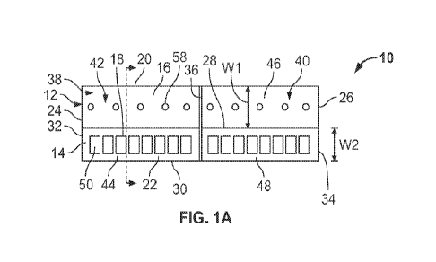
Referring to FIGS. 1A through 2D, in some embodiments, a roofing system 5
includes a
plurality of photovoltaic shingles 10, each of which includes a first layer 12
and a second layer 14
overlaying the first layer 12. In some embodiments, the first layer 12
includes a head lap 16. In
some embodiments, the second layer 14 includes at least one solar cell 18. In
some embodiments,
the at least one solar cell 18 includes a plurality of the solar cells 18. In
some embodiments, at
least one of the plurality of photovoltaic shingles 10 overlays at least the
head lap 16 of another of
the plurality of photovoltaic shingles 10.
Still referring to FIGS. 1A through 2D, in some embodiments, the first layer
12 includes a
first end 20, a second end 22 opposite the first end 20, a third end 24
extending from the first end
of to the second end 22, and a fourth end 26 opposite the third end 24 and
extending from the
first end 20 to the second end 22. In some embodiments, the head lap 16
extends from the third
20 end 24 to the fourth end 26. In some embodiments, the second layer 14
extends from the third end
24 of the first layer 12 to the fourth end 26 of the first layer 12. In some
embodiments, the second
layer 14 extends intermediate the third and fourth ends 24, 26 of the first
layer 12. In some
embodiments, the second layer 14 is located proximate to the second end 22 of
the first layer 12.
11
CA 03191420 2023- 3- 1
WO 2022/051593
PCT/US2021/049017
In an embodiment, the second layer 14 includes a first end 28, a second end 30
opposite
the first end 28, a third end 32 extending from the first end 28 to the second
end 30, and a fourth
end 34 opposite the third end 32 and extending from the first end 28 to the
second end 30. In some
embodiments, the second end 30 of the second layer 14 is substantially aligned
with the second
end 22 of the first layer 12.
In some embodiments, the head lap 16 includes a first width WI and the second
layer 14
includes a second width W2. In some embodiments, the first width WI extends
from the first end
20 of the first layer 12 to the first end 28 of the second layer 14. In some
embodiments, the second
width W2 extends from the first end 28 of the second layer 14 to the second
end 30 of the second
layer 14. In some embodiments, the first width WI is greater than the second
width W2. In some
embodiments, the second width W2 is greater than the first width Wl. In some
embodiments, the
first width WI and the second width W2 are equal to one another.
In some embodiments, the first width WI is in a range of 1 inch to 10 inches.
In some
embodiments, the first width WI is in a range of 2 inches to 10 inches. In
some embodiments, the
first width WI is in a range of 3 inches to 10 inches. In some embodiments,
the first width WI is
in a range of 4 inches to 10 inches. In some embodiments, the first width WI
is in a range of 5
inches to 10 inches. In some embodiments, the first width WI is in a range of
6 inches to 10
inches. In some embodiments, the first width WI is in a range of 7 inches to
10 inches. In some
embodiments, the first width WI is in a range of 8 inches to 10 inches. In
some embodiments, the
first width WI is in a range of 9 inches to 10 inches.
In some embodiments, the first width WI is in a range of 1 inch to 9 inches.
In some
embodiments, the first width WI is in a range of 2 inches to 9 inches. In some
embodiments, the
first width WI is in a range of 3 inches to 9 inches. In some embodiments, the
first width WI is
12
CA 03191420 2023- 3- 1
WO 2022/051593
PCT/US2021/049017
in a range of 4 inches to 9 inches. In some embodiments, the first width WI is
in a range of 5
inches to 9 inches. In some embodiments, the first width W1 is in a range of 6
inches to 9 inches.
In some embodiments, the first width WI is in a range of 7 inches to 9 inches.
In some
embodiments, the first width W1 is in a range of 8 inches to 9 inches.
In some embodiments, the first width WI is in a range of I inch to 8 inches.
In some
embodiments, the first width WI is in a range of 2 inches to 8 inches. In some
embodiments, the
first width W1 is in a range of 3 inches to 8 inches. In some embodiments, the
first width WI is
in a range of 4 inches to 8 inches. In some embodiments, the first width WI is
in a range of 5
inches to 8 inches. In some embodiments, the first width W1 is in a range of 6
inches to 8 inches.
In some embodiments, the first width WI is in a range of 7 inches to 8 inches.
In some embodiments, the first width WI is in a range of 1 inch to 7 inches.
In some
embodiments, the first width WI is in a range of 2 inches to 7 inches. In some
embodiments, the
first width WI is in a range of 3 inches to 7 inches. In some embodiments, the
first width WI is
in a range of 4 inches to 7 inches. In some embodiments, the first width WI is
in a range of 5
inches to 7 inches. In some embodiments, the first width W1 is in a range of 6
inches to 7 inches.
In some embodiments, the first width W1 is in a range of 1 inch to 6 inches.
In some
embodiments, the first width WI is in a range of 2 inches to 6 inches In some
embodiments, the
first width WI is in a range of 3 inches to 6 inches. In some embodiments, the
first width WI is
in a range of 4 inches to 6 inches. In some embodiments, the first width WI is
in a range of 5
inches to 6 inches.
In some embodiments, the first width WI is in a range of 1 inch to 5 inches.
In some
embodiments, the first width WI is in a range of 2 inches to 5 inches. In some
embodiments, the
13
CA 03191420 2023- 3- 1
WO 2022/051593
PCT/US2021/049017
first width W1 is in a range of 3 inches to 5 inches. In some embodiments, the
first width W1 is
in a range of 4 inches to 5 inches.
In some embodiments, the first width W1 is in a range of 1 inch to 4 inches.
In some
embodiments, the first width W1 is in a range of 2 inches to 4 inches In some
embodiments, the
first width W11 is in a range of 3 inches to 4 inches. In some embodiments,
the first width W11 is
in a range of 1 inch to 3 inches. In some embodiments, the first width W1 is
in a range of 2 inches
to 3 inches. In some embodiments, the first width W1 is in a range of 1 inch
to 2 inches.
In some embodiments, the first width W1 is 1 inch. In some embodiments, the
first width
W1 is 2 inches. In some embodiments, the first width W1 is 3 inches. In some
embodiments, the
first width W1 is 4 inches. In some embodiments, the first width W1 is 5
inches. In some
embodiments, the first width W1 is 6 inches. In some embodiments, the first
width W1 is 7 inches.
In some embodiments, the first width W1 is 8 inches. In some embodiments, the
first width W1
is 9 inches. In some embodiments, the first width W1 is 10 inches.
In some embodiments, the second width W2 is in a range of 1 inch to 10 inches.
In some
embodiments, the second width W2 is in a range of 2 inches to 10 inches. In
some embodiments,
the second width W2 is in a range of 3 inches to 10 inches. In some
embodiments, the second
width W2 is in a range of 4 inches to 10 inches. In some embodiments, the
second width W2 is
in a range of 5 inches to 10 inches. In some embodiments, the second width W2
is in a range of 6
inches to 10 inches. In some embodiments, the second width W2 is in a range of
7 inches to 10
inches. In some embodiments, the second width W2 is in a range of 8 inches to
10 inches. In
some embodiments, the second width W2 is in a range of 9 inches to 10 inches.
In some embodiments, the second width W2 is in a range of 1 inch to 9 inches.
In some
embodiments, the second width W2 is in a range of 2 inches to 9 inches. In
some embodiments,
14
CA 03191420 2023- 3- 1
WO 2022/051593
PCT/US2021/049017
the second width W2 is in a range of 3 inches to 9 inches. In some
embodiments, the second width
W2 is in a range of 4 inches to 9 inches. In some embodiments, the second
width W2 is in a range
of 5 inches to 9 inches. In some embodiments, the second width W2 is in a
range of 6 inches to 9
inches. In some embodiments, the second width W2 is in a range of 7 inches to
9 inches. In some
embodiments, the second width W2 is in a range of 8 inches to 9 inches.
In some embodiments, the second width W2 is in a range of 1 inch to 8 inches.
In some
embodiments, the second width W2 is in a range of 2 inches to 8 inches. In
some embodiments,
the second width W2 is in a range of 3 inches to 8 inches. In some
embodiments, the second width
W2 is in a range of 4 inches to 8 inches. In some embodiments, the second
width W2 is in a range
of 5 inches to 8 inches. In some embodiments, the second width W2 is in a
range of 6 inches to 8
inches. In some embodiments, the second width W2 is in a range of 7 inches to
8 inches.
In some embodiments, the second width W2 is in a range of 1 inch to 7 inches.
In some
embodiments, the second width W2 is in a range of 2 inches to 7 inches. In
some embodiments,
the second width W2 is in a range of 3 inches to 7 inches. In some
embodiments, the second width
W2 is in a range of 4 inches to 7 inches. In some embodiments, the second
width W2 is in a range
of 5 inches to 7 inches. In some embodiments, the second width W2 is in a
range of 6 inches to 7
inches.
In some embodiments, the second width W2 is in a range of 1 inch to 6 inches.
In some
embodiments, the second width W2 is in a range of 2 inches to 6 inches. In
some embodiments,
the second width W2 is in a range of 3 inches to 6 inches. In some
embodiments, the second width
W2 is in a range of 4 inches to 6 inches. In some embodiments, the second
width W2 is in a range
of 5 inches to 6 inches.
CA 03191420 2023- 3- 1
WO 2022/051593
PCT/US2021/049017
In some embodiments, the second width W2 is in a range of 1 inch to 5 inches.
In some
embodiments, the second width W2 is in a range of 2 inches to 5 inches. In
some embodiments,
the second width W2 is in a range of 3 inches to 5 inches. In some
embodiments, the second width
W2 is in a range of 4 inches to 5 inches.
In some embodiments, the second width W2 is in a range of I inch to 4 inches.
In some
embodiments, the second width W2 is in a range of 2 inches to 4 inches. In
some embodiments,
the second width W2 is in a range of 3 inches to 4 inches. In some
embodiments, the second width
W2 is in a range of 1 inch to 3 inches. In some embodiments, the second width
W2 is in a range
of 2 inches to 3 inches. In some embodiments, the second width W2 is in a
range of 1 inch to 2
inches.
In some embodiments, the second width W2 is 1 inch. In some embodiments, the
second
width W2 is 2 inches. In some embodiments, the second width W2 is 3 inches. In
some
embodiments, the second width W2 is 4 inches. In some embodiments, the second
width W2 is 5
inches. In some embodiments, the second width W2 is 6 inches. In some
embodiments, the second
width W2 is 7 inches. In some embodiments, the second width W2 is 8 inches. In
some
embodiments, the second width W2 is 9 inches. In some embodiments, the second
width W2 is
10 inches.
Still referring to FIGS. IA through 2D, in some embodiments, each of the
plurality of
photovoltaic shingles 10 includes a fold line 36 extending from the first end
20 of the first layer
12 to the second end 22 of the first layer 12 and intermediate the third and
fourth ends 24, 26 of
the first layer 12. In some embodiments, the fold line 36 extends from and
through the first end
28 of the second layer 14 to the second end 30 of the second layer 14. In some
embodiments, the
fold line 36 enables the photovoltaic shingle 10 to be folded in half for
reduction of space in
16
CA 03191420 2023- 3- 1
WO 2022/051593
PCT/US2021/049017
connection with the storage or transport of the photovoltaic shingle 10. In
some embodiments,
each of the plurality of photovoltaic shingles 10 includes a first section 38
extending from the third
end 24 of the first layer 12 to the fold line 36, and a second section 40
extending from the fourth
end 26 of the first layer 12 to the fold line 36. In some embodiments, the
first section 38 includes
a first portion 42 of the head lap 16 and a first portion 44 of the second
layer 14, and the second
section 40 includes a second portion 46 of the head lap 16 and a second
portion 48 of the second
layer 14. In some embodiments, the at least one solar cell 18 includes a first
one 50 of the at least
one solar cell 18 located in the first portion 44 of the second layer 14 and a
second one 52 of the
at least one solar cell 18 located in the second portion 48 of the second
layer 14. In some
embodiments, the first one 50 of the at least one solar cell 18 includes a
first plurality of the solar
cells 18, and the second one 52 of the at least one solar cell 18 includes a
second plurality of the
solar cells 18.
Referring to FIGS. 2A and 2C, in some embodiments, the second layer 14 extends
intermediate the third and fourth ends 24, 26 of the first layer 12. In some
embodiments, the first
layer includes a first step flap 54 adjacent the third end 32 of the second
layer 14 and a second step
flap 56 adjacent the fourth end 34 of the second layer 14. In some
embodiments, the first step flap
54 includes a length Ll extending from the third end 32 of the second layer 14
to the third end 24
of the first layer 12. In some embodiments, the first step flap 54 includes a
width W3 extending
from the first end 20 of the first layer 12 to the second end 22 of the first
layer 12. In some
embodiments, the second step flap 56 includes a length L2 extending from the
fourth end 34 of
the second layer 14 to the fourth end 26 of the first layer 12. In some
embodiments, the second
step flap 56 includes a width W4 extending from the first end 20 of the first
layer 12 to the second
end 22 of the first layer 12. In some embodiments, the width W3 is equal to
the width W4. In
17
CA 03191420 2023- 3- 1
WO 2022/051593
PCT/US2021/049017
some embodiments, the length L1 and is equal to the length L2. In some
embodiments, the head
lap 16, the first step flap 54, and the second step flap 56 are contiguous.
In some embodiments, the second layer 14 extends from the third end 24 of the
first layer
12 to a location intermediate the third and fourth ends 24, 26 of the first
layer 12. In some
embodiments, the first layer 12 includes the second step flap 56 adjacent the
fourth end 34 of the
second layer 14. In some embodiments, the head lap 16 and the second step flap
56 are contiguous.
In some embodiments, the second layer 14 extends from the fourth end 26 of the
first layer 12 to
a location intermediate the third and fourth ends 24, 26 of the first layer
12. In some embodiments,
the first layer 12 includes the first step flap 54 adjacent the third end 32
of the second layer 14. In
some embodiments, the head lap 16 and the first step flap 54 are contiguous.
In some embodiments, each of the first layer 12 and the second layer 14 is
composed of a
polymer. In some embodiments, each of the first layer 12 and the second layer
14 is composed of
thermoplastic polyolefin (TPO). In some embodiments, each of the first layer
12 and the second
layer 14 is composed of polyethylene terephthalate (PET), polyethylene
naphthalate (PEN),
polyetheretherketone (PEEK), polyaryletherketone (PAEK), polyarylate (PAR),
polyetherimide
(PEI), polyarylsulfone (PAS), polyethersulfone (PES), polyamideimide (PAT), or
polyimide;
polyvinyl chloride (PVC); ethylene propylene diene monomer (EPDN4) rubber;
silicone rubber;
fluoropolymers - ethylene tetrafluoroethylene (ETFE), polyvinylidene fluoride
(P \e'DF),
tetrafluoroethylene-hexafluoropropylene copolymers (FEP), and
tetrafluoroethylene-
hexafluoropropylene-vinylidene fluoride copolymers (THV), or blends thereof.
In some embodiments, the first layer 12 and the second layer 14 are laminated.
In some
embodiments, the second layer 14 is ultrasonically welded to the first layer
12. In some
18
CA 03191420 2023- 3- 1
WO 2022/051593
PCT/US2021/049017
embodiments, the second layer 14 is heat welded to the first layer 12. In some
embodiments, the
second layer 14 is thermally bonded to the first layer 12.
In some embodiments, an impact resistance of the photovoltaic shingle 10 is
characterized
by a Class 4 rating in accordance with the standards of ANSI FM 4473 test
standards.
In some embodiments, the plurality of photovoltaic shingles 10 is installed on
a roof deck
200. In some embodiments, the plurality of photovoltaic shingles 10 is
installed directly to the
roof deck 200. In some embodiments, each of the plurality of photovoltaic
shingles 10 is installed
on the roof deck 200 by a plurality of fasteners 58. In some embodiments, the
plurality of fasteners
58 are installed through the head lap 16. In some embodiments, the plurality
of fasteners 58
includes a plurality of nails.
Referring to FIG. 2E, in some embodiments, each of the plurality of
photovoltaic shingles
10 is installed on the roof deck 200 by an adhesive 60. In some embodiments,
the adhesive 60 is
adhered directly to the roof deck 200. In some embodiments, the adhesive 60 is
adhered to an
underlayment. In some embodiments, the underlayment is adhered directly to the
roof deck 200.
In some embodiments, the adhesive 60 is located on a rear surface 62 of the
photovoltaic shingle
10. In some embodiments, the adhesive 60 includes at least one adhesive strip.
In some
embodiments, the adhesive 60 includes a plurality of adhesive strips. In some
embodiments, the
plurality of adhesive strips is arranged intermittently. In some embodiments,
the adhesive 60 is
located proximate to one edge of the photovoltaic shingle 10. In some
embodiments, the adhesive
60 is a peel and stick film sheet. In some embodiments, the peel and stick
film sheet includes at
least one sheet of film removably attached to the rear surface 62. In some
embodiments, the peel
and stick film sheet is composed of EverGuard Freedom HW peel and stick
membrane
manufactured by GAF. In some embodiments, the adhesive 60 includes polyvinyl
butyrate,
19
CA 03191420 2023- 3- 1
WO 2022/051593
PCT/US2021/049017
acrylic, silicone, or polycarbonate. In some embodiments, the adhesive 60
includes pressure
sensitive adhesives.
In some embodiments, the system 5 includes an underlayment layer 202 installed
on the
roof deck 200 (see FIG. 6). In some embodiments, the plurality of photovoltaic
shingles 10
overlay the underlayment layer 202.
Referring to FIGS. 1A through 1D, in some embodiments, one of the plurality of
photovoltaic shingles 10 overlays the head lap 16 of another of the plurality
of photovoltaic
shingles 10. In some embodiments, one of the plurality of photovoltaic
shingles 10 overlays the
first section 38 and the second section 40 of the another of the of the
plurality of photovoltaic
shingles 10 for a staggered installation of the photovoltaic shingles 10. In
some embodiments, the
first section 38 of the one of the plurality of photovoltaic shingles 10
overlays the first section 38
and the second section 40 of the another of the of the plurality of
photovoltaic shingles 10. In
some embodiments, the second section 40 of the one of the plurality of
photovoltaic shingles 10
overlays the first section 38 and the second section 40 of the another of the
of the plurality of
photovoltaic shingles 10.
Referring to FIGS. 2A through 2D, in some embodiments, the first step flap 54
of one of
the plurality of photovoltaic shingles 10 overlays the first step flap 54 of
another of the plurality
of photovoltaic shingles 10, and the second step flap 56 of the one of the
plurality of photovoltaic
shingles 10 overlays the second step flap 56 of the another of the plurality
of photovoltaic shingles
10 for a non-staggered installation of the photovoltaic shingles 10. In some
embodiments, the first
step flap 54 of the one of the plurality of photovoltaic shingles 10
substantially aligns with the first
step flap 54 of the another of the plurality of photovoltaic shingles 10, and
the second step flap 56
of the one of the plurality of photovoltaic shingles 10 substantially aligns
with the second step flap
CA 03191420 2023- 3- 1
WO 2022/051593
PCT/US2021/049017
56 of the another of the plurality of photovoltaic shingles 10. In some
embodiments, the third end
32 of the second layer 14 of the one of the plurality of photovoltaic shingles
10 substantially aligns
with the third end 32 of the second layer 14 of the another of the plurality
of photovoltaic shingles
10, and the fourth end 34 of the second layer 14 of the one of the plurality
of photovoltaic shingles
10 substantially aligns with the fourth end 34 of the second layer 14 of the
another of the plurality
of photovoltaic shingles 10. In some embodiments, the second step flap 56 of
one of the plurality
of photovoltaic shingles 10 overlays the first step flap 54 of another of the
plurality of photovoltaic
shingles 10.
In some embodiments, each of the plurality of photovoltaic shingles 10 meets
the standards
of Florida Testing Application Standard (TAS) 100-95 when tested in accordance
therewith.
In some embodiments, each of the plurality of photovoltaic shingles includes a
height H1
in a range of 5 mm to 20 mm. In some embodiments, each of the plurality of
photovoltaic shingles
includes a height H1 in a range of 6 mm to 20 mm. In some embodiments, each of
the plurality
of photovoltaic shingles includes a height HI in a range of 7 mm to 20 mm. In
some embodiments,
each of the plurality of photovoltaic shingles includes a height H1 in a range
of 8 mm to 20 mm.
In some embodiments, each of the plurality of photovoltaic shingles includes a
height H1 in a
range of 9 mm to 20 mm In some embodiments, each of the plurality of
photovoltaic shingles
includes a height HI in a range of 10 mm to 20 mm. In some embodiments, each
of the plurality
of photovoltaic shingles includes a height H1 in a range of 11 mm to 20 mm. In
some
embodiments, each of the plurality of photovoltaic shingles includes a height
H1 in a range of 12
mm to 20 mm. In some embodiments, each of the plurality of photovoltaic
shingles includes a
height HI in a range of 13 mm to 20 mm. In some embodiments, each of the
plurality of
photovoltaic shingles includes a height H1 in a range of 14 mm to 20 mm. In
some embodiments,
21
CA 03191420 2023- 3- 1
WO 2022/051593
PCT/US2021/049017
each of the plurality of photovoltaic shingles includes a height HI in a range
of 15 mm to 20 mm.
In some embodiments, each of the plurality of photovoltaic shingles includes a
height HI in a
range of 16 mm to 20 mm. In some embodiments, each of the plurality of
photovoltaic shingles
includes a height in a range of 17 mm to 20 mm. In some embodiments, each of
the plurality of
photovoltaic shingles includes a height HI in a range of 18 mm to 20 mm. In
some embodiments,
each of the plurality of photovoltaic shingles includes a height HI in a range
of 19 mm to 20 mm.
In some embodiments, each of the plurality of photovoltaic shingles includes a
height H1
in a range of 5 mm to 19 mm. In some embodiments, each of the plurality of
photovoltaic shingles
includes a height HI in a range of 6 mm to 19 mm. In some embodiments, each of
the plurality
of photovoltaic shingles includes a height HI in a range of 7 mm to 19 mm. In
some embodiments,
each of the plurality of photovoltaic shingles includes a height HI in a range
of 8 mm to 19 mm.
In some embodiments, each of the plurality of photovoltaic shingles includes a
height HI in a
range of 9 mm to 19 mm. In some embodiments, each of the plurality of
photovoltaic shingles
includes a height HI in a range of 10 mm to 19 mm. In some embodiments, each
of the plurality
of photovoltaic shingles includes a height HI in a range of 11 mm to 19 mm. In
some
embodiments, each of the plurality of photovoltaic shingles includes a height
HI in a range of 12
mm to 19 mm. In some embodiments, each of the plurality of photovoltaic
shingles includes a
height HI in a range of 13 mm to 19 mm. In some embodiments, each of the
plurality of
photovoltaic shingles includes a height HI in a range of 14 mm to 19 mm. In
some embodiments,
each of the plurality of photovoltaic shingles includes a height HI in a range
of 15 mm to 19 mm.
In some embodiments, each of the plurality of photovoltaic shingles includes a
height HI in a
range of 16 mm to 19 mm. In some embodiments, each of the plurality of
photovoltaic shingles
22
CA 03191420 2023- 3- 1
WO 2022/051593
PCT/US2021/049017
includes a height H1 in a range of 17 mm to 19 mm. In some embodiments, each
of the plurality
of photovoltaic shingles includes a height 111 in a range of 18 mm to 19 mm.
In some embodiments, each of the plurality of photovoltaic shingles includes a
height H1
in a range of 5 mm to 18 mm. In some embodiments, each of the plurality of
photovoltaic shingles
includes a height 1-11 in a range of 6 mm to 18 mm. In some embodiments, each
of the plurality
of photovoltaic shingles includes a height 111 in a range of 7 mm to 18 mm. In
some embodiments,
each of the plurality of photovoltaic shingles includes a height Ill in a
range of 8 mm to 18 mm.
In some embodiments, each of the plurality of photovoltaic shingles includes a
height Ill in a
range of 9 mm to 18 mm. In some embodiments, each of the plurality of
photovoltaic shingles
includes a height 111 in a range of 10 mm to 18 mm. In some embodiments, each
of the plurality
of photovoltaic shingles includes a height 111 in a range of 11 mm to 18 mm.
In some
embodiments, each of the plurality of photovoltaic shingles includes a height
111 in a range of 12
mm to 18 mm. In some embodiments, each of the plurality of photovoltaic
shingles includes a
height HI in a range of 13 mm to 18 mm. In some embodiments, each of the
plurality of
photovoltaic shingles includes a height 111 in a range of 14 mm to 18 mm. In
some embodiments,
each of the plurality of photovoltaic shingles includes a height 111 in a
range of 15 mm to 18 mm.
In some embodiments, each of the plurality of photovoltaic shingles includes a
height HI in a
range of 16 mm to 18 mm. In some embodiments, each of the plurality of
photovoltaic shingles
includes a height 111 in a range of 17 mm to 18 mm.
In some embodiments, each of the plurality of photovoltaic shingles includes a
height H1
in a range of 5 mm to 17 mm. In some embodiments, each of the plurality of
photovoltaic shingles
includes a height HI in a range of 6 mm to 17 mm. In some embodiments, each of
the plurality
of photovoltaic shingles includes a height 111 in a range of 7 mm to 17 mm. In
some embodiments,
23
CA 03191420 2023- 3- 1
WO 2022/051593
PCT/US2021/049017
each of the plurality of photovoltaic shingles includes a height 111 in a
range of 8 mm to 17 mm.
In some embodiments, each of the plurality of photovoltaic shingles includes a
height 111 in a
range of 9 mm to 17 mm. In some embodiments, each of the plurality of
photovoltaic shingles
includes a height 111 in a range of 10 mm to 17 mm. In some embodiments, each
of the plurality
of photovoltaic shingles includes a height HI in a range of Ii mm to 17 mm. In
some
embodiments, each of the plurality of photovoltaic shingles includes a height
111 in a range of 12
mm to 17 mm. In some embodiments, each of the plurality of photovoltaic
shingles includes a
height Ill in a range of 13 mm to 17 mm. In some embodiments, each of the
plurality of
photovoltaic shingles includes a height H1 in a range of 14 mm to 17 mm. In
some embodiments,
each of the plurality of photovoltaic shingles includes a height 111 in a
range of 15 mm to 17 mm.
In some embodiments, each of the plurality of photovoltaic shingles includes a
height 111 in a
range of 16 mm to 17 mm.
In some embodiments, each of the plurality of photovoltaic shingles includes a
height 131
in a range of 5 mm to 16 mm. In some embodiments, each of the plurality of
photovoltaic shingles
includes a height 111 in a range of 6 mm to 16 mm. In some embodiments, each
of the plurality
of photovoltaic shingles includes a height 111 in a range of 7 mm to 16 mm. In
some embodiments,
each of the plurality of photovoltaic shingles includes a height HI in a range
of 8 mm to 16 mm.
In some embodiments, each of the plurality of photovoltaic shingles includes a
height HI in a
range of 9 mm to 16 mm. In some embodiments, each of the plurality of
photovoltaic shingles
includes a height 111 in a range of 10 mm to 16 mm. In some embodiments, each
of the plurality
of photovoltaic shingles includes a height 111 in a range of 11 mm to 16 mm.
In some
embodiments, each of the plurality of photovoltaic shingles includes a height
HI in a range of 12
mm to 16 mm. In some embodiments, each of the plurality of photovoltaic
shingles includes a
24
CA 03191420 2023- 3- 1
WO 2022/051593
PCT/US2021/049017
height 111 in a range of 13 mm to 16 mm. In some embodiments, each of the
plurality of
photovoltaic shingles includes a height Ill in a range of 14 mm to 16 mm. In
some embodiments,
each of the plurality of photovoltaic shingles includes a height 111 in a
range of 15 mm to 16 mm.
In some embodiments, each of the plurality of photovoltaic shingles includes a
height 111
in a range of 5 mm to IS mm. In some embodiments, each of the plurality of
photovoltaic shingles
includes a height 111 in a range of 6 mm to 15 mm. In some embodiments, each
of the plurality
of photovoltaic shingles includes a height 111 in a range of 7 mm to 15 mm. In
some embodiments,
each of the plurality of photovoltaic shingles includes a height 111 in a
range of 8 mm to 15 mm.
In some embodiments, each of the plurality of photovoltaic shingles includes a
height 111 in a
range of 9 mm to 15 mm. In some embodiments, each of the plurality of
photovoltaic shingles
includes a height 111 in a range of 10 mm to 15 mm. In some embodiments, each
of the plurality
of photovoltaic shingles includes a height 111 in a range of 11 mm to 15 mm.
In some
embodiments, each of the plurality of photovoltaic shingles includes a height
111 in a range of 12
mm to 15 mm. In some embodiments, each of the plurality of photovoltaic
shingles includes a
height 111 in a range of 13 mm to 15 mm. In some embodiments, each of the
plurality of
photovoltaic shingles includes a height 111 in a range of 14 mm to 15 mm.
In some embodiments, each of the plurality of photovoltaic shingles includes a
height HI
in a range of 5 mm to 14 mm. In some embodiments, each of the plurality of
photovoltaic shingles
includes a height 111 in a range of 6 mm to 14 mm. In some embodiments, each
of the plurality
of photovoltaic shingles includes a height 111 in a range of 7 mm to 14 mm. In
some embodiments,
each of the plurality of photovoltaic shingles includes a height 111 in a
range of 8 mm to 14 mm.
In some embodiments, each of the plurality of photovoltaic shingles includes a
height HI in a
range of 9 mm to 14 mm. In some embodiments, each of the plurality of
photovoltaic shingles
CA 03191420 2023- 3- 1
WO 2022/051593
PCT/US2021/049017
includes a height H1 in a range of 10 mm to 14 mm. In some embodiments, each
of the plurality
of photovoltaic shingles includes a height H1 in a range of 11 mm to 14 mm. In
some
embodiments, each of the plurality of photovoltaic shingles includes a height
H1 in a range of 12
mm to 14 mm. In some embodiments, each of the plurality of photovoltaic
shingles includes a
height I-11 in a range of 13 mm to 14 mm.
In some embodiments, each of the plurality of photovoltaic shingles includes a
height H1
in a range of 5 mm to 13 mm. In some embodiments, each of the plurality of
photovoltaic shingles
includes a height H1 in a range of 6 mm to 13 mm. In some embodiments, each of
the plurality
of photovoltaic shingles includes a height HI in a range of 7 mm to 13 mm. In
some embodiments,
each of the plurality of photovoltaic shingles includes a height H1 in a range
of 8 mm to 13 mm.
In some embodiments, each of the plurality of photovoltaic shingles includes a
height 111 in a
range of 9 mm to 13 mm. In some embodiments, each of the plurality of
photovoltaic shingles
includes a height H1 in a range of 10 mm to 13 mm. In some embodiments, each
of the plurality
of photovoltaic shingles includes a height HI in a range of 11 mm to 13 mm. In
some
embodiments, each of the plurality of photovoltaic shingles includes a height
H1 in a range of 12
mm to 13 mm.
In some embodiments, each of the plurality of photovoltaic shingles includes a
height H1
in a range of 5 mm to 12 mm. In some embodiments, each of the plurality of
photovoltaic shingles
includes a height H1 in a range of 6 mm to 12 mm. In some embodiments, each of
the plurality
of photovoltaic shingles includes a height H1 in a range of 7 mm to 12 mm. In
some embodiments,
each of the plurality of photovoltaic shingles includes a height H1 in a range
of 8 mm to 12 mm.
In some embodiments, each of the plurality of photovoltaic shingles includes a
height HI in a
range of 9 mm to 12 mm. In some embodiments, each of the plurality of
photovoltaic shingles
26
CA 03191420 2023- 3- 1
WO 2022/051593
PCT/US2021/049017
includes a height H1 in a range of 10 mm to 12 mm. In some embodiments, each
of the plurality
of photovoltaic shingles includes a height H1 in a range of 11 mm to 12 mm.
In some embodiments, each of the plurality of photovoltaic shingles includes a
height H1
in a range of 5 mm to 11 mm. In some embodiments, each of the plurality of
photovoltaic shingles
includes a height 1-11 in a range of 6 mm to ii mm. In some embodiments, each
of the plurality
of photovoltaic shingles includes a height 111 in a range of 7 mm to 11 mm. In
some embodiments,
each of the plurality of photovoltaic shingles includes a height Ill in a
range of 8 mm to 11 mm.
In some embodiments, each of the plurality of photovoltaic shingles includes a
height Ill in a
range of 9 mm to 11 mm. In some embodiments, each of the plurality of
photovoltaic shingles
includes a height 111 in a range of 10 mm to 11 mm.
In some embodiments, each of the plurality of photovoltaic shingles includes a
height HI
in a range of 5 mm to 10 mm. In some embodiments, each of the plurality of
photovoltaic shingles
includes a height 111 in a range of 6 mm to 10 mm. In some embodiments, each
of the plurality
of photovoltaic shingles includes a height HI in a range of 7 mm to 10 mm. In
some embodiments,
each of the plurality of photovoltaic shingles includes a height 111 in a
range of 8 mm to 10 mm.
In some embodiments, each of the plurality of photovoltaic shingles includes a
height 111 in a
range of 9 mm to 10 mm.
In some embodiments, each of the plurality of photovoltaic shingles includes a
height HI
in a range of 5 mm to 9 mm. In some embodiments, each of the plurality of
photovoltaic shingles
includes a height 111 in a range of 6 mm to 9 mm. In some embodiments, each of
the plurality of
photovoltaic shingles includes a height 111 in a range of 7 mm to 9 mm. In
some embodiments,
each of the plurality of photovoltaic shingles includes a height HI in a range
of 8 mm to 9 mm.
27
CA 03191420 2023- 3- 1
WO 2022/051593
PCT/US2021/049017
In some embodiments, each of the plurality of photovoltaic shingles includes a
height HI
in a range of 5 mm to 8 mm. In some embodiments, each of the plurality of
photovoltaic shingles
includes a height HI in a range of 6 mm to 8 mm. In some embodiments, each of
the plurality of
photovoltaic shingles includes a height HI in a range of 7 mm to 8 mm.
In some embodiments, each of the plurality of photovoltaic shingles includes a
height HI
in a range of 5 mm to 7 mm. In some embodiments, each of the plurality of
photovoltaic shingles
includes a height HI in a range of 6 mm to 7 mm. In some embodiments, each of
the plurality of
photovoltaic shingles includes a height HI in a range of 5 mm to 6 mm.
In some embodiments, each of the plurality of photovoltaic shingles includes a
height HI
of 5 mm. In some embodiments, each of the plurality of photovoltaic shingles
includes a height
HI of 6 mm. In some embodiments, each of the plurality of photovoltaic
shingles includes a height
HI of 7 mm. In some embodiments, each of the plurality of photovoltaic
shingles includes a height
HI of 8 mm. In some embodiments, each of the plurality of photovoltaic
shingles includes a height
HI of 9 mm. In some embodiments, each of the plurality of photovoltaic
shingles includes a height
HI of 10 mm. In some embodiments, each of the plurality of photovoltaic
shingles includes a
height HI of 11 mm. In some embodiments, each of the plurality of photovoltaic
shingles includes
a height H1 of 12 mm. In some embodiments, each of the plurality of
photovoltaic shingles
includes a height HI of 13 mm. In some embodiments, each of the plurality of
photovoltaic
shingles includes a height HI of 14 mm. In some embodiments, each of the
plurality of
photovoltaic shingles includes a height HI of 15 mm. In some embodiments, each
of the plurality
of photovoltaic shingles includes a height HI of 16 mm. In some embodiments,
each of the
plurality of photovoltaic shingles includes a height HI of 17 mm. In some
embodiments, each of
the plurality of photovoltaic shingles includes a height HI of 18 mm. In some
embodiments, each
28
CA 03191420 2023- 3- 1
WO 2022/051593
PCT/US2021/049017
of the plurality of photovoltaic shingles includes a height H1 of 19 mm. In
some embodiments,
each of the plurality of photovoltaic shingles includes a height H1 of 20 mm.
Referring to FIGS. 3A through 5, in some embodiments, the system 5 includes at
least one
wireway 100 installed proximate to the plurality of photovoltaic shingles 10
on the roof deck 200.
In some embodiments, the at least one wireway 100 is installed intermediate
the plurality of
photovoltaic shingles 10. In some embodiments, the at least one wireway 100 is
installed
proximate to each of the third ends 32 of the second layers 14. In some
embodiments, the at least
one wireway 100 overlays each of the first step flaps 54. In some embodiments,
the at least one
wireway 100 is installed proximate to each of the fourth ends 34 of the second
layers 14. In some
embodiments, the at least one wireway 100 overlays each of the second step
flaps 56. In some
embodiments, the at least one wireway 100 is installed intermediate each of
the third ends 32 of a
first plurality of the photovoltaic shingles 10 and the fourth ends 34 of a
second plurality of the
photovoltaic shingles 10. In some embodiments, the at least one wireway 100
overlays each of
the first step flaps 54. In some embodiments, the at least one wireway 100
overlays each of the
second step flaps 56. In some embodiments, the step flaps 54, 56 form the
wireway 100.
Referring to FIGS. 6 through 11, in some embodiments, the at least one wireway
100
includes a pair of rails 102 spaced apart from one another. In some
embodiments, the rails 102
extend outwardly from the roof deck 200. In some embodiments, the rails 102
are substantially
parallel to another. In some embodiments, each of the rails 102 includes side
flashing 104. In
some embodiments, each of the side flashing 104 includes a first portion 106
positioned on the
roof deck 200 and second portion 108 extending obliquely and inwardly in a
first direction relative
to the first portion 106. In some embodiments, slots 109 are formed between
the first portions 106
and the second portions 108. In some embodiments, the at least one wireway 100
is rectangular
29
CA 03191420 2023- 3- 1
WO 2022/051593
PCT/US2021/049017
in shape. In some embodiments, the photovoltaic shingles 10 overlay the second
portion 108 of
the side flashing 104. In some embodiments, the at least one wireway 100 is
sized and shaped to
receive electrical components of a photovoltaic system, such as an electrical
junction box,
electrical wire, and electrical connectors.
Still referring to FIGS. 6 through 11, in some embodiments, the at least one
wireway 100
includes a lid 110. In some embodiments, the lid 110 is removably attached to
the at least one
wireway 100. In some embodiments, the lid 110 includes a cover portion 112 and
a pair of rails
114 spaced apart from one another and extending obliquely and inwardly in a
second direction
opposite the first direction of the second portion 108 of the rails 102. In
some embodiments, the
lid 110 is removably engaged with the side flashing 104 of the wireway 100
such that the rails 114
of the lid 110 engage (e.g., snap-in) the second portions 108 of the side
flashing 104. In some
embodiments, the lid 110 is substantially rectangular in shape. In some
embodiments, the rails
114 extend outwardly and obliquely in the first direction. In some
embodiments, the lid 110 is
removably attached to the at least one wireway 100 by screws, nails, rivets,
adhesives or other
fasteners.
In some embodiments, the at least one wireway 100 includes a plurality of
wireways 100.
In some embodiments, one of the lids 110 of one of the plurality of wireways
100 overlaps another
of the lids HO of another of the plurality of wireways 100 (see FIGS. 9
through H). In some
embodiments, the overlapping lids 110 promote water shedding. In some
embodiments, the at
least one wireway 100 is moisture resistant. As used herein, the term
"moisture resistant" means
having a water transmission rate of less than or equal to 0.05 U.S. perms, as
measured by ASTM
E 96, Procedure B ¨ Standard Test Methods for Water Vapor Transmission of
Materials. In some
embodiments, the wireway 100 withstands walking loads/step resistance that
conforms to
CA 03191420 2023- 3- 1
WO 2022/051593
PCT/US2021/049017
standards under UL 3741 test standards (UL Standard for Safety Photovoltaic
Hazard Control). In
some embodiments, the wireway 100 includes an axe impact resistance that
conforms to standards
under UL 3741 test standards. In some embodiments, the wireway 100 includes a
body fall
resistance that conforms to standards under UL 3741 test standards.
In certain embodiments, the lid 110 includes a plurality of louvers 116 See
FIGS. 12C
and 12D. In some embodiments, the louvers 116 are formed within the rails 114
of the lid 110. In
some embodiments, the louvers 116 are formed within the cover portion 112. In
some
embodiments, the louvers 116 are elongated. In some embodiments, the louvers
116 are
rectangular in shape. In some embodiments, the louvers 116 are semi-circular
in shape.
In some embodiments, the lid 110 includes at least one support member 118
extending
from an interior surface 120 of the cover portion 112. In some embodiments,
the at least one
support member 118 includes a plurality of support members. In some
embodiments, each of the
plurality of support members 118 is spaced apart from one another. In some
embodiments, each
of the plurality of support members 118 is oriented in at least two opposing
rows (see FIGS. 10
and 11). In some embodiments, the at least one support member 118 is integral
with the cover
portion 112. In some embodiments, the at least one support member 118 is
formed by crimping a
section of the cover portion 112 (see FIGS. 12A and 13A). In some embodiments,
the at least one
support member 118 is attached to the interior surface 120 of the cover
portion 112 (see FIGS.
12B and 13B). In some embodiments, the at least one support member 118 is
attached to the
interior surface 120 of the cover portion 112 by welding. In some embodiments,
the at least one
support member 118 is attached to the interior surface 120 of the cover
portion 112 by an adhesive.
In some embodiments, the at least one support member 118 includes a T-rail
shape.
31
CA 03191420 2023- 3- 1
WO 2022/051593
PCT/US2021/049017
Referring to FIGS. 14A through 14C, In some embodiments, the lid 110 is
attached to the
first layer 12 of one the photovoltaic shingles 10 by an adhesive 121. In some
embodiments, the
lid 110 includes a hook member 122. In some embodiments, the hook member 122
includes an
upper rail 124 and a lower rail 126 spaced apart from and substantially
parallel to the upper rail
124. In some embodiments, the hook member 122 is removably positioned
intermediate the first
layer 12 of one of the plurality of photovoltaic shingles 10 and the second
layer 14 of the one of
the plurality of photovoltaic shingles 10 such that the second layer 14 is
positioned between the
upper and lower rails 124, 126.
Referring to FIGS. 14D and 14E, in some embodiments, the wireway 100 includes
a length
Li of 100 mm to 450 mm. In some embodiments, the wireway 100 includes a length
Li of 100
mm to 400 mm. In some embodiments, the wireway 100 includes a length Li of 100
mm to 350
mm. In some embodiments, the wireway 100 includes a length Li of 100 mm to 300
mm. In
some embodiments, the wireway 100 includes a length Li of 100 mm to 250 mm. In
some
embodiments, the wireway 100 includes a length Li of 100 mm to 200 mm. In some
embodiments,
the wireway 100 includes a length Li of 100 mm to 150 mm.
In some embodiments, the wireway 100 includes a length Li of 150 mm to 450 mm.
In
some embodiments, the wireway 100 includes a length Ll of 150 mm to 400 mm. In
some
embodiments, the wireway 100 includes a length Li of 150 mm to 350 mm. In some
embodiments,
the wireway 100 includes a length Li of 150 mm to 300 mm. In some embodiments,
the wireway
100 includes a length Li of 150 mm to 250 mm. In some embodiments, the wireway
100 includes
a length Li of 150 mm to 200 mm.
In some embodiments, the wireway 100 includes a length Li of 200 mm to 450 mm.
In
some embodiments, the wireway 100 includes a length Li of 200 mm to 400 mm. In
some
32
CA 03191420 2023- 3- 1
WO 2022/051593
PCT/US2021/049017
embodiments, the wireway 100 includes a length L1 of 200 mm to 350 mm. In some
embodiments,
the wireway 100 includes a length Li of 200 mm to 300 mm. In some embodiments,
the wireway
100 includes a length Li of 200 mm to 250 mm.
In some embodiments, the wireway 100 includes a length Li of 250 mm to 450 mm.
In
some embodiments, the wireway 100 includes a length Ll of 250 mm to 400 mm. In
some
embodiments, the wireway 100 includes a length Li of 250 mm to 350 mm. In some
embodiments,
the wireway 100 includes a length Li of 250 mm to 300 mm.
In some embodiments, the wireway 100 includes a length Li of 300 mm to 450 mm.
In
some embodiments, the wireway 100 includes a length Li of 300 mm to 400 mm. In
some
embodiments, the wireway 100 includes a length Li of 300 mm to 350 mm.
In some
embodiments, the wireway 100 includes a length Li of 350 mm to 450 mm. In some
embodiments,
the wireway 100 includes a length Li of 350 mm to 400 mm. In some embodiments,
the wireway
100 includes a length Li of 400 mm to 450 mm.
In some embodiments, the wireway 100 includes a width WI of 100 mm to 200 mm.
In
some embodiments, the wireway 100 includes a width WI of 100 mm to 175 mm. In
some
embodiments, the wireway 100 includes a width W1 of 100 mm to 150 mm. In some
embodiments, the wireway 100 includes a width W1 of 100 mm to 125 mm.
In some embodiments, the wireway 100 includes a width WI of 125 mm to 200 mm.
In
some embodiments, the wireway 100 includes a width WI of 125 mm to 175 mm. In
some
embodiments, the wireway 100 includes a width WI of 125 mm to 150 mm. In some
embodiments, the wireway 100 includes a width WI of 150 mm to 200 mm. In some
embodiments, the wireway 100 includes a width WI of 150 mm to 175 mm. In some
embodiments, the wireway 100 includes a width WI of 175 mm to 200 mm.
33
CA 03191420 2023- 3- 1
WO 2022/051593
PCT/US2021/049017
In some embodiments, the wireway 100 includes a height H1 of 5 mm to 25 mm. In
some
embodiments, the wireway 100 includes a height H1 of 5 mm to 20 mm. In some
embodiments,
the wireway 100 includes a height H1 of 5 mm to 15 mm. In some embodiments,
the wireway
100 includes a height H1 of 5 mm to 10 mm.
In some embodiments, the wireway 100 includes a height 1-11 of 10 mm to 25 mm.
In some
embodiments, the wireway 100 includes a height H1 of 10 mm to 20 mm. In some
embodiments,
the wireway 100 includes a height H1 of 10 mm to 15 mm. In some embodiments,
the wireway
100 includes a height H1 of 15 mm to 25 mm. In some embodiments, the wireway
100 includes
a height H1 of 15 mm to 20 mm. In some embodiments, the wireway 100 includes a
height H1 of
20 mm to 25 mm.
In some embodiments, the wireway 100 is composed of a polymeric material. In
some
embodiments, the wireway 100 is composed of polypropylene. In some
embodiments, the
wireway 100 is composed of polyethylene. In some embodiments, the wireway 100
is composed
of polyethylene. In some embodiments, the wireway 100 is composed of metal. In
some
embodiments, the wireway 100 is composed of aluminum.
In some embodiments, the wireway 100 includes a fire resistance that conforms
to
standards under UL 94 test standards. In some embodiments, the wireway 100
includes a fire-
resistance having a V-0 rating in accordance with the standards of UL 94 test
standards. In some
embodiments, the wireway 100 includes a fire-resistance having a V-1 rating in
accordance with
the standards of UL 94 test standards. In some embodiments, the wireway 100
includes a fire-
resistance having a V-2 rating in accordance with the standards of UL 94 test
standards. in some
embodiments, the photovoltaic shingle 10 is a component of a
roofing/photovoltaic system that
conforms to standards under UL 790/ASTM E 108 test standards. In some
embodiments, the
34
CA 03191420 2023- 3- 1
WO 2022/051593
PCT/US2021/049017
roofing/photovoltaic system includes a fire-resistance having a Class A rating
in accordance with
the standards of UL 790/ASTM E 108 test standards.
Referring to FIGS. 15A through 16, in some embodiments, the outer surface 119
of the
cover portion 112 of the lid 110 includes at least one band 128. In some
embodiments, the at least
one band 128 includes a first color. In some embodiments, the first color is
different from a color
of a remainder of the outer surface 119. In some embodiments, the lid 110
includes a first end
130, a second end 132 opposite the first end 130, a third end 134 extending
from the first end 130
to the second end 132, and a fourth end 136 extending from the first end 130
to the second end
132.
In some embodiments, one of the at least one band 128 extends from the first
end 130 to
the second end 132. In some embodiments, the one of the at least one band 128
is proximate to
the third end 134. See FIG. 15A. In some embodiments, the one of the at least
one band 128 is
proximate to the fourth end 136. See FIG. 15B. In some embodiments, the one of
the at least one
band 128 is intermediate the third end 134 and the fourth end 136. See FIG.
15C. In some
embodiments, one of the at least one band 128 extends from the third end 134
to the fourth end
136. In some embodiments, the one of the at least one band 128 is proximate to
the first end 130.
In some embodiments, the one of the at least one band 128 is proximate to the
second end 132. In
some embodiments, the at least one band 128 includes a second band 128,
wherein the second
band 128 extends from the first end 130 to the second end 132. In some
embodiments, the second
band 128 is proximate to the third end 134. In some embodiments, the second
band 128 is
proximate to the fourth end 136. In some embodiments, the second band 128 is
intermediate the
third end 134 and the fourth end 136. In some embodiments, the bands 128 mimic
the appearance
of the photovoltaic shingles 10 to provide a blended aesthetic look between
the lids 110, the
CA 03191420 2023- 3- 1
WO 2022/051593
PCT/US2021/049017
photovoltaic shingles 10, and a plurality of roofing shingles 204 of the
roofing system 5 (see FIG.
16).
Referring to FIGS. 17A through 18B, in some embodiments, the at least one
solar cell 18
includes an electrical bussing 140 and at least one electrical connector 142
electrically connected
to the electrical bussing 140. In some embodiments, the at least one
electrical connector 142 is
positioned on the head lap 16. In some embodiments, the at least one
electrical connector 142
includes a first electrical connector 142a and a second electrical connector
142b. In some
embodiments, the first electrical connector 142a is positioned proximate to
the third end 24 and
the second electrical connector 142b is positioned proximate to the fourth end
26. In some
embodiments, the first electrical connector 142a of one of the plurality of
photovoltaic shingles 10
is connected to the second electrical connector 142b of another of the
plurality of photovoltaic
shingles 10. In some embodiments, the first electrical connector 142a is a
male connector and the
second electrical connector 142b is a female connector. In some embodiments,
the first and second
electrical connectors 142a, 142b are connected to one another by an electrical
wire 144 (see FIGS.
17A and 17B). In some embodiments, the first and second electrical connectors
142a, 142b are
removably connected to one another. In some embodiments, the first and second
electrical
connectors 142a, 142b are USB connectors (see FIGS. 18A and 18B). In some
embodiments,
when the photovoltaic shingles 10 are installed to the roof deck 200, each of
the electrical
connectors 142 are positioned within a corresponding space 206 formed between
one of the
photovoltaic shingles 10 and another overlapping one of the photovoltaic
shingles 10.
Referring to FIG. 19, in some embodiments, the system 5 includes step flashing
208
installed on the roof deck 200. In some embodiments, the step flashing 208
includes a first portion
210 and a second portion 212. In some embodiments, the photovoltaic shingle 10
overlays the
36
CA 03191420 2023- 3- 1
WO 2022/051593
PCT/US2021/049017
first portion 210, while one of the roofing shingles 204 overlays the second
portion 212. In some
embodiments, the roofing shingles 204 include asphalt shingles. Referring to
FIGS. 20, 21A and
21B, in some embodiments, the one of the roofing shingles 204 overlays one of
the step flaps 54,
56 of a corresponding one of the photovoltaic shingles 10. In some
embodiments, the plurality of
photovoltaic shingles 10 is coplanar with the plurality of roofing shingles
204. As used herein, the
term "coplanar" means the plurality of photovoltaic shingles 10 and the
plurality of roofing
shingles 204 are positioned and extend within the same plane, or the plurality
of photovoltaic
shingles 10 is positioned and extends in a first plane, and the plurality of
roofing shingles 204 is
positioned and extends within a second plane that is offset from the first
plane of a relatively of no
more than ten percent of a height measured from the roof deck to an upper
surface of the plurality
of photovoltaic shingles.
In some embodiments, a method of installing a photovoltaic system includes the
following
steps:
= obtaining a first photovoltaic shingle and a second photovoltaic shingle,
each of
which includes a first layer, and a second layer overlaying the first layer,
wherein the first layer
includes a head lap, wherein the second layer includes at least one solar
cell;
= installing the first photovoltaic shingle on a roof deck; and
= overlaying the second photovoltaic shingle on at least the head lap of
the first
photovoltaic shingle.
In some embodiments, the method of installing the photovoltaic system may
include the
step of installing a wireway proximate to the plurality of photovoltaic
shingles. In some
embodiments, the method of installing the photovoltaic system may include the
step of installing
at least one electrical junction box installed within the at least one
wireway. In some embodiments,
37
CA 03191420 2023- 3- 1
WO 2022/051593
PCT/US2021/049017
the method of installing the photovoltaic system may include the step of
installing at least one lid
on the at least one wireway.
Referring to FIGS. 22A through 22D, in some embodiments, a method of
installing a
photovoltaic system includes the following steps:
= obtaining a first photovoltaic shingle, a second photovoltaic shingle, a
third
photovoltaic shingle, and fourth photovoltaic shingle, each of which includes
a first layer, and a
second layer overlaying the first layer, wherein the first layer includes a
head lap and a step flap,
wherein the second layer includes at least one solar cell;
= installing a junction box on the step flap of the first photovoltaic
shingle,
= installing the second photovoltaic shingle on a roof deck;
= installing the first photovoltaic shingle on the roof deck by overlaying
the step flap
of the second photovoltaic shingle with the step flap of the first
photovoltaic shingle;
= installing a junction box on the step flap of the third photovoltaic
shingle;
= installing the fourth photovoltaic shingle on the roof deck by overlaying
the fourth
photovoltaic shingle on at least the head lap of the second photovoltaic
shingle;
= installing the third photovoltaic shingle on the roof deck by overlaying
the step flap
of the third photovoltaic shingle with the step flap of the fourth
photovoltaic shingle and overlaying
the third photovoltaic shingle on at least the head lap of the first
photovoltaic shingle.
In some embodiments, the method of installing the photovoltaic system may
include the
step of covering each of the step flaps and junction boxes with a
corresponding lid.
Referring to FIGS. 23A through 23D, in some embodiments, a method of
installing a
photovoltaic system includes the following steps:
38
CA 03191420 2023- 3- 1
WO 2022/051593
PCT/US2021/049017
= obtaining a first photovoltaic shingle, a second photovoltaic shingle, a
third
photovoltaic shingle, and a fourth photovoltaic shingle, each of which
includes a first layer, and a
second layer overlaying the first layer, wherein the first layer includes a
head lap, wherein the
second layer includes at least one solar cell, and wherein each of the first
photovoltaic shingle and
the third photovoltaic shingle includes a wireway located at a first end
thereof;
= installing a junction box on each of the corresponding wireways of the
first and
third photovoltaic shingles;
= installing the first photovoltaic shingle on a roof deck;
= installing the second photovoltaic shingle on the roof deck such that a
first end of
the second photovoltaic shingle abuts the wireway of the first photovoltaic
shingle;
= installing the third photovoltaic shingle on the roof deck by overlaying
the third
photovoltaic shingle on at least the head lap of the first photovoltaic
shingle; and
= installing the fourth photovoltaic shingle on the roof deck such that a
first end of
the fourth photovoltaic shingle abuts the wireway of the third photovoltaic
shingle and overlays at
least the head lap of the second photovoltaic shingle.
In some embodiments, the method of installing the photovoltaic system may
include the
step of covering each of the wireways and junction boxes with a corresponding
lid.
In some embodiments, a method of installing a photovoltaic system includes the
following
steps:
= Obtaining a plurality of photovoltaic shingles, with each photovoltaic
shingle of the
plurality of the photovoltaic shingles including a first end, a first layer
including a head lap portion,
a second layer overlaying the first layer, the second layer including at least
one solar cell,
39
CA 03191420 2023- 3- 1
WO 2022/051593
PCT/US2021/049017
= Laying a first photovoltaic shingle of the plurality of photovoltaic
shingles directly
on a deck surface of a steep slope roof
= Attaching the first photovoltaic shingle of the plurality of photovoltaic
shingles to
the deck surface of the steep slope roof.
= Laying
a second photovoltaic shingle of the plurality of photovoltaic shingles over
at least a part of the head lap portion of the first photovoltaic shingle of
the plurality of photovoltaic
shingles.
= Attaching the second photovoltaic shingle to the deck surface of the
steep slope
roof to form a roof integrated photovoltaic system.
As defined herein, a "steep slope roof' is any roof substrate that is disposed
on a roof
having a pitch of Y/X, where Y and X are in a ratio of 4:12 to 12:12, where Y
corresponds to the
"rise" of the roof, and where X corresponds to the "run" of the roof.
In some embodiments, Y and X are in a ratio of 5:12 to 12:12. In some
embodiments, Y
and X are in a ratio of 6:12 to 12:12. In some embodiments, Y and X are in a
ratio of 7:12 to
12:12. In some embodiments, Y and X are in a ratio of 6:12 to 12:12. In some
embodiments, Y
and X are in a ratio of 8: 1 2 to 12:12. In some embodiments, Y and X are in a
ratio of 6:12 to 12:12.
In some embodiments, Y and X are in a ratio of 9:12 to 12:12. In some
embodiments, Y and X are
in a ratio of 10:12 to 12:12. In some embodiments, Y and X are in a ratio of
11:12 to 12:12.
In some embodiments, Y and X are in a ratio of 4:12 to 11:12. In some
embodiments,
Y and X are in a ratio of 4:12 to 10:12. In some embodiments, Y and X are in a
ratio of 4:12 to
9:12. In some embodiments, Y and X are in a ratio of 4:12 to 8:12. In some
embodiments, Y and
X are in a ratio of 4:12 to 7:12. In some embodiments, Y and X are in a ratio
of 4:12 to 6:12. In
some embodiments, Y and X are in a ratio of 4:12 to 5:12.
CA 03191420 2023- 3- 1
WO 2022/051593
PCT/US2021/049017
lJ
In some embodiments, Y and X are in a ratio of 5:12 to 11:12. In some
embodiments, Y
and X are in a ratio of 6:12 to 10:12. In some embodiments, Y and X are in a
ratio of 7:12 to 9:12.
In some embodiments, Y and X are in a ratio of 2:12. In some embodiments, Y
and X are
in a ratio of 3:12.
Referring to FIG. 24, in some embodiments, a roofing system 310 includes a
plurality of
solar shingles 312 arranged in a plurality of rows, a plurality of roofing
shingles 314, and a plurality
of wireways 300. In some embodiments, the plurality of rows of the solar
shingles 312 includes
an upper row R1 and a lower row R2. In some embodiments, each of the wireways
300 includes
a length Ll. In some embodiments, the length Li extends from the lower row R2
to the upper
row Rl. In some embodiments, the length Li extends from the lower row R2 to at
least to the
upper row Rl. In some embodiments, the length Li extends from the lower row R2
to a location
past the upper row Rl. In some embodiments, the wireways 300 includes a lid
316. In some
embodiments, the lid 316 is a single lid that extends the length Ll.
Referring to FIGS. 25 through 27, in some embodiments, a wireway 400 includes
a bracket
402 and a lid 404 attached removably to the bracket 402. In some embodiments,
the bracket 402
includes a body 406 having a first end 408, a second end 410 opposite the
first end 408, and a pair
of side edges 412, 414 extending from the first end 408 to the second end 410.
In some
embodiments, the body 406 is rectangular in shape. In some embodiments, the
body 406 includes
a first alignment portion 416 located proximate to the first end 408 and a
second alignment portion
418 located proximate to the second end 410. In some embodiments, the first
alignment portion
416 includes a base 419 and a tab 420 connected to the base 419 and extending
outwardly and
spaced from a surface 421 of the body 406. In some embodiments, the tab 420
includes an L-
41
CA 03191420 2023- 3- 1
WO 2022/051593
PCT/US2021/049017
shape. In some embodiments, the second alignment portion 418 includes a slot
422. In some
embodiments, the slot 422 is rectangular in shape.
In some embodiments, the bracket 402 includes a plurality of clips 424. In
some
embodiments, the plurality of clips 424 extends outwardly from the surface
421. In some
embodiments, each of the plurality of clips 424 is curvilinear in shape and
includes a slot 426. In
some embodiments, the slot 426 is sized and shaped to receive and hold an
electrical wire or cable
therein. In some embodiments, one of the plurality of clips 424 is located
proximate to the first
end 408 and another of the plurality of clips 424 is located proximate to the
second end 410. In
some embodiments, the bracket 402 includes a plurality of stops 428 located
proximate to the
second end 410. In some embodiments, one of the plurality of stops 428 is
located proximate to
the first end 408 and another of the plurality of stops 428 is located
proximate to the second end
410. In some embodiments, the bracket 402 includes a plurality of hold down
portions 430. In
some embodiments, one of the plurality of hold down portions 430 is located
proximate to the first
end 408 and another of the plurality of hold down portions 430 is located
proximate to the second
end 410. In some embodiments, each of the hold down portions 430 extends from
a first end 432,
located proximate to the second end 410, and to a second end 434, located
intermediate the first
end 408 and the second end 410. In some embodiments, each of the hold down
portions 430
includes a stepped surface 43L In some embodiments, each of the stepped
surfaces 431 provides
clearance for an adjacent photovoltaic shingle.
Referring to FIG. 27, in some embodiments, the lid 404 includes a first
portion 436 and
side portions 438 extending from the first portion 436. In some embodiments,
the side portions
438 are angled (i.e., oblique) relative to the first portion 436. In some
embodiments, the side
portions 438 are angled to prevent shading over adjacent photovoltaic cells.
In some embodiments,
42
CA 03191420 2023- 3- 1
WO 2022/051593
PCT/US2021/049017
each of the side portions 438 includes a tab portion 440 that is sized and
shaped to removably
engage a corresponding one of the hold down portions 430 of the bracket 402.
In some
embodiments, the lid 404 includes a plurality of support members 442 extending
from an interior
surface 444 of the lid 404 In some embodiments, each of the plurality of
support members 442
engages a corresponding one of the plurality of stops 428 of the bracket 402.
In some
embodiments, air is permitted to enter the wireway 400 through the side edges
412, 414 for
ventilation, since the hold down portions 430 do not extend the entire length
of the wireway 400.
Referring to FIG. 28, in some embodiments, a plurality of the wireways 400 are
connected
to one another. In some embodiments, the slot 422 of one of the plurality of
wireways 400 is sized
and shaped to receive the tab 420 of an adjacent one of another of the
plurality of wireways 400 to
maintain alignment of the plurality of wireways 400 with one another.
Referring to FIGS. 29 through 31, in some embodiments, a lid 510 for a wireway
includes
a first end 512 and a second end 514 opposite the first end 512, and an
extended portion 516
extending from the first end 512. In some embodiments, the extended portion
516 includes a cross-
section similar to the remaining portion 518 of the lid 510, except that ends
of side portions 520
of the extended portion 516 are offset from ends of the side portions 522 of
the lid 510. In some
embodiments, the second end 514 of one of the lids 510 is sized and shaped to
overlay the extended
portion 516 of another of the lids 510 such that the second end 514 of the one
of the lids 510 is
aligned with the first end 512 of the other of the lids 510. In some
embodiments, the lid 510
includes a first stop 511 extending from an interior surface of the lid 510
and located proximate to
the first end 512 for alignment with the second end 514 of an adjacent one of
the lids 510. In some
embodiments, the lid 510 includes a pair of second stops 513 extending from
the interior surface
of the lid 510 and located proximate to the second end 514. Referring to FIG.
32, in some
43
CA 03191420 2023- 3- 1
WO 2022/051593
PCT/US2021/049017
embodiments, an end cap 526 includes a body 528 having a first end 530 and a
second end 532
opposite the first end 530, and a plurality of vents 534 extending from the
first end 530 to the
second end 532. In some embodiments, the second end 514 of the lid 510 is
sized and shaped to
receive the end cap 526 In some embodiments, the second stops 513 prevent the
end cap 526
from being pushed too far within the lid 510 and fully past the second end
514. In some
embodiments, the plurality of vents 534 permit air flow within the wireway. In
some
embodiments, the lid 510 includes a centrally located third stop 515 for
support and stability of
the lid 510 on the wireway.
Referring to FIGS. 33 and 34, in some embodiments, a lid 600 for a wireway
includes a
base 602 having a first surface 604 and a second surface 606 opposite the
first surface 604. In
some embodiments, the base 602 is square in shape. In some embodiments, the
base 602 is
rectangular in shape. In some embodiments, the lid 600 includes a cover
portion 608 extending
outwardly from the first surface 604. In some embodiments, the cover portion
608 is integral with
the base 602. In some embodiments, the cover portion 608 is sized and shaped
to cover an end of
a wireway. In some embodiments, the cover portion 608 is sized and shaped to
cover a wireway
located at an end of a column of a plurality of wireways. In some embodiments,
the lid 600
includes a pair of side flaps 610. In some embodiments, one or more roofing
shingles are
configured to overlay each of the side flaps 610. In some embodiments, an
electrical component
is configured to overlay either of the side flaps 610. In some embodiments,
the electrical
component is a junction box. In some embodiments, the electrical component is
at least one
electrical connector. In some embodiments, the lid 600 includes a head lap
612. In some
embodiments, one or more roofing shingles are configured to overlay the head
lap 612. In some
embodiments, an electrical component is configured to overlay the head lap
612. In some
44
CA 03191420 2023- 3- 1
WO 2022/051593
PCT/US2021/049017
embodiments, an electrical component is configured to overlay the head lap
612. In some
embodiments, the electrical component is an electrical termination box.
Referring to FIGS. 35A and 35B, in some embodiments, a lid 700 for a wireway
includes
a first portion 702 and a second portion 704 overlaying the first portion 702.
In some
embodiments, the lid 700 includes opposed sidewalls 706. In some embodiments,
the sidewalls
706 include a curvilinear profile. In some embodiments, the sidewalls 706
include a linear profile.
In some embodiments, the first portion 702 is composed of an opaque material.
In some
embodiments, the second portion 704 is composed of a transparent material. In
some
embodiments, the second portion 704 is composed of a translucent material. In
some
embodiments, the second portion 704 includes a coating. In some embodiments,
the second
portion 704 is composed of a polymer gel. In some embodiments, the first
portion 702 and the
second portion 704 are laminated with one another. In some embodiments, the
lid 700 is
configured to mimic the appearance of a photovoltaic module having a glass
layer.
Referring to FIGS. 36A and 36B, in some embodiments, a lid 800 for a wireway
includes
opposed sidewalls 806. In some embodiments, the each of the sidewalls 806
includes a plurality
of surfaces 808. In some embodiments, the plurality of surfaces 808 includes
linear surfaces 810.
In some embodiments, the linear surfaces 810 form an angled pattern. In some
embodiments, the
plurality of surfaces 808 includes curvilinear surfaces 812. In some
embodiments, the plurality of
surfaces 808 form a sinusoidal pattern. In some embodiments, each of the
plurality of surfaces
808 is configured to create shadows on the sidewalls 806 to provide a
consistent tone of the lid
800 and enable the lid 800 to blend in with other components of a roofing
system, such as roofing
shingles and photovoltaic shingles.
CA 03191420 2023- 3- 1
WO 2022/051593
PCT/US2021/049017
Referring to FIGS. 37A and 37B, in some embodiments, a lid 900 for a wireway
includes
opposed sidewalls 906. In some embodiments, each of the sidewalls 906 includes
a plurality of
fins 908. In some embodiments, the plurality of fins 908 is configured to
dissipate heat from and
within the wireway. In some embodiments, the plurality of fins 908 includes an
angular profile
910. In some embodiments, the plurality of fins 908 includes a curvilinear
profile 912. In some
embodiments, the plurality of fins 908 includes a rectangular profile 914
(e.g., similar to a heat
sink).
Referring to FIGS. 38A and 38B, in some embodiments, a lid 1000 for a wireway
includes
an upper portion 1002 and pair of sidewalls 1004 extending from the upper
portion 1002. In some
embodiments, each of the sidewalls 1004 includes a rail 1006 that extends the
length of the lid
1000 and forms a slot 1008 between the rail 1006 and the upper portion 1002.
In some
embodiments, an insert 1010 is sized and shaped to be slidably received within
the slots 1008 and
over the upper portion 1002. In some embodiments, the insert 1010 is
rectangular in shape. In
some embodiments, the insert 1010 is flat. In some embodiments, the insert
1010 is U-shaped. In
some embodiments, the insert 1010 includes asphalt material. In some
embodiments, the insert
1010 includes an appearance that mimics the appearance of an asphalt roofing
shingle. In some
embodiments, the insert 1010 includes a photovoltaic cell. In some
embodiments, the insert 1010
includes an appearance that mimics the appearance of a photovoltaic cell. In
some embodiments,
the insert 1010 includes a printed graphic.
Referring to FIGS. 39A and 39B, in some embodiments, a photovoltaic module
1110
includes an active area 1109 having a plurality of solar cells 1112. In some
embodiments, the
photovoltaic module 1110 includes an inactive area comprising a headlap
portion 1113, a first side
lap 1115 located at one end of the photovoltaic module 1110, and a second side
lap 1117 located
46
CA 03191420 2023- 3- 1
WO 2022/051593
PCT/US2021/049017
at an opposite end of the photovoltaic module 1110. In some embodiments, the
headlap portion
1113 is textured. In some embodiments, the texture of the headlap portion 1113
is different from
a texture of the solar cells 1112. In some embodiments, a wire cover bracket
1300 is attached to
the first side lap 1115. In some embodiments, the wire cover bracket 1300
includes a junction box
1423. Details of the wire cover bracket 1300 shall be provided hereinbelow.
In some embodiments, the plurality of solar cells 1112 includes a first set of
solar cells
1112a and a second set of solar cells 1112b. In some embodiments, the first
set of solar cells
1112a includes eight of the solar cells 1112. In some embodiments, the second
set of solar cells
1112b includes eight of the solar cells 1112. In some embodiments, each of the
first set of solar
cells 1112a and the second set of solar cells 1112b includes more or less than
eight of the solar
cells 1112. In some embodiments, a last one of the solar cells 1112 of the
first set of solar cells
1112a is separated by a first one of the solar cells 1112 of the second set of
solar cells 1112b by a
space S. In some embodiments, the space S is located approximately half the
length of the
photovoltaic module 1110. In some embodiments, the solar cells 1112 of each of
the first and
second sets of solar cells 1112a, 1112b are strung together with bussing 1101.
In some
embodiments, the bussing 1101 includes nine bussing wires. In some
embodiments, the bussing
1101 may include more or less than the nine bussing wires.
In some embodiments, a first bussing wire 1103a extends from the first side
lap 1115 to
the space S. In some embodiments, the first bussing wire 1103a extends to
approximately half the
length of the photovoltaic module 1110. In some embodiments, one end of the
first bussing wire
1103a is electrically connected to the junction box 1423 and the other end of
the first bussing wire
1103a is electrically connected to the first set of solar cells 1112a. In some
embodiments, a second
bussing wire 1103b extends from the first side lap 1115 to a location
proximate to the second side
47
CA 03191420 2023- 3- 1
WO 2022/051593
PCT/US2021/049017
lap 1117. In some embodiments, the second bussing wire 1103b extends
substantially the entire
length of the photovoltaic module 1110. In some embodiments, one end of the
second bussing
wire 1103b is electrically connected to the junction box 1423 and the other
end of the second
bussing wire 1103b is electrically connected to the second set of solar cells
1112b. In some
embodiments, each of the first bussing wire 1103a and the second bussing wire
1103b is covered
with a polymer layer. In some embodiments, each of the first bussing wire
1103a and the second
bussing wire 1103b is covered with expanded polyethylene ("ETU). In some
embodiments, the
EPE is comprised of a black strip In some embodiments, each of the first
bussing wire 1103a and
the second bussing wire 1103b is coated with a colorant or dye to reduce
reflectivity.
In some embodiments, the plurality of solar cells 1112 includes a plurality of
the solar cells
1112. In some embodiments, the plurality of solar cells 1112 is arranged in
one row (i.e., one
reveal). In some embodiments, the plurality of solar cells 1112 is arranged in
two rows (i.e., two
reveals). In some embodiments, the plurality of solar cells 1112 is arranged
in three rows (i.e.,
three reveals). In some embodiments, the plurality of solar cells 1112 is
arranged in four rows
(i.e., four reveals). In some embodiments, the plurality of solar cells 1112
is arranged in five rows
(i.e., five reveals). In some embodiments, the plurality of solar cells 1112
is arranged in six rows
(i.e., six reveals). In some embodiments, the plurality of solar cells 1112 is
arranged in more than
six rows.
Referring to FIG. 40, in some embodiments, the active area 1109 of the
photovoltaic
module 1110 includes the plurality of solar cells 1112, an encapsulant 1114
encapsulating the
plurality of solar cells 1112, and a frontsheet 1116 juxtaposed with the
encapsulant 1114. In some
embodiments, the frontsheet 1116 is juxtaposed with a first surface of the
encapsulant 1114. As
used herein, the terms "encapsulating" and "encapsulates" mean to partially or
fully envelope or
48
CA 03191420 2023- 3- 1
WO 2022/051593
PCT/US2021/049017
enclose, and with respect to certain embodiments of the photovoltaic module
1110, the plurality
of solar cells 1112 is fully enveloped by or enclosed within the encapsulant
1114, or partially
enveloped by or enclosed within the encapsulant 1114. In some embodiments, the
plurality of
solar cells 1112 includes a plurality of the solar cells 1112. In some
embodiments, the encapsulant
1114 encapsulates 50% to 99.9% of an exterior surface area of the plurality of
solar cells 1112. In
some embodiments, the encapsulant 1114 encapsulates 55% to 99.9% of an
exterior surface area
of the plurality of solar cells 1112. In some embodiments, the encapsulant
1114 encapsulates 60%
to 99.9% of an exterior surface area of the plurality of solar cells 1112. In
some embodiments, the
encapsulant 1114 encapsulates 65% to 99.9% of an exterior surface area of the
plurality of solar
cells 1112. In some embodiments, the encapsulant 1114 encapsulates 70% to
99.9% of an exterior
surface area of the plurality of solar cells 1112. In some embodiments, the
encapsulant 1114
encapsulates 75% to 99.9% of an exterior surface area of the plurality of
solar cells 1112. In some
embodiments, the encapsulant 1114 encapsulates 80% to 99.9% of an exterior
surface area of the
plurality of solar cells 1112. In some embodiments, the encapsulant 1114
encapsulates 85% to
99.9% of an exterior surface area of the plurality of solar cells 1112. In
some embodiments, the
encapsulant 1114 encapsulates 90% to 99.9% of an exterior surface area of the
plurality of solar
cells 1112. In some embodiments, the encapsulant 1114 encapsulates 95% to
99.9% of an exterior
surface area of the plurality of solar cells 1112.
In some embodiments, the encapsulant 1114 encapsulates 50% to 95% of an
exterior
surface area of the plurality of solar cells 1112. In some embodiments, the
encapsulant 1114
encapsulates 55% to 95% of an exterior surface area of the plurality of solar
cells 1112. In some
embodiments, the encapsulant 1114 encapsulates 60% to 95% of an exterior
surface area of the
plurality of solar cells 1112. In some embodiments, the encapsulant 1114
encapsulates 65% to
49
CA 03191420 2023- 3- 1
WO 2022/051593
PCT/US2021/049017
95% of an exterior surface area of the plurality of solar cells 1112. In some
embodiments, the
encapsulant 1114 encapsulates 70% to 95% of an exterior surface area of the
plurality of solar cells
1112. In some embodiments, the encapsulant 1114 encapsulates 75% to 95% of an
exterior surface
area of the plurality of solar cells 1112. In some embodiments, the
encapsulant 1114 encapsulates
80% to 95% of an exterior surface area of the plurality of solar cells 1112.
In some embodiments,
the encapsulant 1114 encapsulates 85% to 95% of an exterior surface area of
the plurality of solar
cells 1112. In some embodiments, the encapsulant 1114 encapsulates 90% to 95%
of an exterior
surface area of the plurality of solar cells 1112.
In some embodiments, the encapsulant 1114 encapsulates 50% to 90% of an
exterior
surface area of the plurality of solar cells 1112. In some embodiments, the
encapsulant 1114
encapsulates 55% to 90% of an exterior surface area of the plurality of solar
cells 1112. In some
embodiments, the encapsulant 1114 encapsulates 60% to 90% of an exterior
surface area of the
plurality of solar cells 1112. In some embodiments, the encapsulant 1114
encapsulates 65% to
90% of an exterior surface area of the plurality of solar cells 1112. In some
embodiments, the
encapsulant 1114 encapsulates 70% to 90% of an exterior surface area of the
plurality of solar cells
1112. In some embodiments, the encapsulant 1114 encapsulates 75% to 90% of an
exterior surface
area of the plurality of solar cells 1112. In some embodiments, the
encapsulant 1114 encapsulates
80% to 90% of an exterior surface area of the plurality of solar cells 1112.
In some embodiments,
the encapsulant 1114 encapsulates 85% to 90% of an exterior surface area of
the plurality of solar
cells 1112.
In some embodiments, the encapsulant 1114 encapsulates 50% to 85% of an
exterior
surface area of the plurality of solar cells 1112. In some embodiments, the
encapsulant 1114
encapsulates 55% to 85% of an exterior surface area of the plurality of solar
cells 1112. In some
CA 03191420 2023- 3- 1
WO 2022/051593
PCT/US2021/049017
embodiments, the encapsulant 1114 encapsulates 60% to 85% of an exterior
surface area of the
plurality of solar cells 1112. In some embodiments, the encapsulant 1114
encapsulates 65% to
85% of an exterior surface area of the plurality of solar cells 1112. In some
embodiments, the
encapsulant 1114 encapsulates 70% to 85% of an exterior surface area of the
plurality of solar cells
1112. In some embodiments, the encapsulant 1114 encapsulates 75% to 85% of
an exterior
surface area of the plurality of solar cells 1112. In some embodiments, the
encapsulant 1114
encapsulates 80% to 85% of an exterior surface area of the plurality of solar
cells 1112.
In some embodiments, the encapsulant 1114 encapsulates 50% to 80% of an
exterior
surface area of the plurality of solar cells 1112. In some embodiments, the
encapsulant 1114
encapsulates 55% to 80% of an exterior surface area of the plurality of solar
cells 1112. In some
embodiments, the encapsulant 1114 encapsulates 60% to 80% of an exterior
surface area of the
plurality of solar cells 1112. In some embodiments, the encapsulant 1114
encapsulates 65% to
80% of an exterior surface area of the plurality of solar cells 1112. In some
embodiments, the
encapsulant 1114 encapsulates 70% to 80% of an exterior surface area of the
plurality of solar cells
1112. In some embodiments, the encapsulant 1114 encapsulates 75% to 80% of an
exterior surface
area of the plurality of solar cells 1112.
In some embodiments, the encapsulant 1114 encapsulates 50% to 75% of an
exterior
surface area of the plurality of solar cells 1112. In some embodiments, the
encapsulant 1114
encapsulates 55% to 75% of an exterior surface area of the plurality of solar
cells 1112. In some
embodiments, the encapsulant 1114 encapsulates 60% to 75% of an exterior
surface area of the
plurality of solar cells 1112. In some embodiments, the encapsulant 1114
encapsulates 65% to
75% of an exterior surface area of the plurality of solar cells 1112. In some
embodiments, the
51
CA 03191420 2023- 3- 1
WO 2022/051593
PCT/US2021/049017
encapsulant 1114 encapsulates 70% to 75% of an exterior surface area of the
plurality of solar cells
1112.
In some embodiments, the encapsulant 1114 encapsulates 50% to 70% of an
exterior
surface area of the plurality of solar cells 1112. In some embodiments, the
encapsulant 1114
encapsulates 55% to 70% of an exterior surface area of the plurality of solar
cells 1112. In some
embodiments, the encapsulant 1114 encapsulates 60% to 70% of an exterior
surface area of the
plurality of solar cells 1112. In some embodiments, the encapsulant 1114
encapsulates 65% to
70% of an exterior surface area of the plurality of solar cells 1112.
In some embodiments, the encapsulant 1114 encapsulates 50% to 65% of an
exterior
surface area of the plurality of solar cells 1112. In some embodiments, the
encapsulant 1114
encapsulates 55% to 65% of an exterior surface area of the plurality of solar
cells 1112. In some
embodiments, the encapsulant 1114 encapsulates 60% to 65% of an exterior
surface area of the
plurality of solar cells 1112. In some embodiments, the encapsulant 1114
encapsulates 50% to
60% of an exterior surface area of the plurality of solar cells 1112. In some
embodiments, the
encapsulant 1114 encapsulates 55% to 60% of an exterior surface area of the
plurality of solar cells
1112. In some embodiments, the encapsulant 1114 encapsulates 55% to 60% of an
exterior surface
area of the plurality of solar cells 1112.
In some embodiments, the encapsulant 1114 encapsulates 50% of an exterior
surface area
of the plurality of solar cells 1112. In some embodiments, the encapsulant
1114 encapsulates 55%
of the exterior surface area of the plurality of solar cells 1112. In some
embodiments, the
encapsulant 1114 encapsulates 60% of the exterior surface area of the
plurality of solar cells 1112.
In some embodiments, the encapsulant 1114 encapsulates 65% of the exterior
surface area of the
plurality of solar cells 1112. In some embodiments, the encapsulant 1114
encapsulates 70% of the
52
CA 03191420 2023- 3- 1
WO 2022/051593
PCT/US2021/049017
exterior surface area of the plurality of solar cells 1112. In some
embodiments, the encapsulant
1114 encapsulates 75% of the exterior surface area of the plurality of solar
cells 1112. In some
embodiments, the encapsulant 1114 encapsulates 80% of the exterior surface
area of the plurality
of solar cells 1112. In some embodiments, the encapsulant 1114 encapsulates
85% of the exterior
surface area of the plurality of solar cells 1112. In some embodiments, the
encapsulant 1114
encapsulates 90% of the exterior surface area of the plurality of solar cells
1112. In some
embodiments, the encapsulant 1114 encapsulates 95% of the exterior surface
area of the plurality
of solar cells 1112. In some embodiments, the encapsulant 1114 encapsulates
100% of the exterior
surface area of the plurality of solar cells 1112.
In some embodiments, the encapsulant 1114 has a thickness of 0.5 mm to 4 mm.
In some
embodiments, the encapsulant 1114 has a thickness of 0.5 mm to 3.5 mm. In some
embodiments,
the encapsulant 1114 has a thickness of 0.5 mm to 3 mm. In some embodiments,
the encapsulant
1114 has a thickness of 0.5 mm to 2.5 mm. In some embodiments, the encapsulant
1114 has a
thickness of 0.5 mm to 2 mm. In some embodiments, the encapsulant 1114 has a
thickness of 0.5
mm to 1.5 mm. In some embodiments, the encapsulant 1114 has a thickness of 0.5
mm to 1 mm.
In some embodiments, the encapsulant 1114 has a thickness of 1 mm to 4 mm. In
some
embodiments, the encapsulant 1114 has a thickness of 1 mm to 3.5 mm. In some
embodiments,
the encapsulant 1114 has a thickness of 1 mm to 3 mm. In some embodiments, the
encapsulant
1114 has a thickness of 1 mm to 2.5 mm. In some embodiments, the encapsulant
1114 has a
thickness of 1 mm to 2 mm. In some embodiments, the encapsulant 1114 has a
thickness of 1 mm
to 1.5 mm. In some embodiments, the encapsulant 1114 has a thickness of 1.5 mm
to 4 mm. In
some embodiments, the encapsulant 1114 has a thickness of 1.5 mm to 3.5 mm. In
some
embodiments, the encapsulant 1114 has a thickness of 1.5 mm to 3 mm. In some
embodiments,
53
CA 03191420 2023- 3- 1
WO 2022/051593
PCT/US2021/049017
the encapsulant 1114 has a thickness of 1.5 mm to 2.5 mm. In some embodiments,
the encapsulant
1114 has a thickness of 1.5 mm to 2 mm.
In some embodiments, the encapsulant 1114 has a thickness of 2 mm to 4 mm. In
some
embodiments, the encapsulant 1114 has a thickness of 2 mm to 3.5 mm. In some
embodiments,
the encapsulant 1114 has a thickness of 2 mm to 3 mm. In some embodiments, the
encapsulant
1114 has a thickness of 2 mm to 2.5 mm. In some embodiments, the encapsulant
1114 has a
thickness of 2.5 mm to 4 mm. In some embodiments, the encapsulant 1114 has a
thickness of 2.5
mm to 3.5 mm. In some embodiments, the encapsulant 1114 has a thickness of 2.5
mm to 3 mm.
In some embodiments, the encapsulant 1114 has a thickness of 3 mm to 4 mm. In
some
embodiments, the encapsulant 1114 has a thickness of 3 mm to 3.5 mm. In some
embodiments,
the encapsulant 1114 has a thickness of 3.5 mm to 4 mm.
In some embodiments, the encapsulant 1114 has a thickness of 0.5 mm. In some
embodiments, the encapsulant 1114 has a thickness of 0.6 mm. In some
embodiments, the
encapsulant 1114 has a thickness of 0.7 mm. In some embodiments, the
encapsulant 1114 has a
thickness of 0.8 mm. In some embodiments, the encapsulant 1114 has a thickness
of 0.9 mm. In
some embodiments, the encapsulant 1114 has a thickness of 1 mm. In some
embodiments, the
encapsulant 1114 has a thickness of 1.5 mm. In some embodiments, the
encapsulant 1114 has a
thickness of 2 mm. In some embodiments, the encapsulant 1114 has a thickness
of 2.5 mm. In
some embodiments, the encapsulant 1114 has a thickness of 3 mm. In some
embodiments, the
encapsulant 1114 has a thickness of 3.5 mm. In some embodiments, the
encapsulant 1114 has a
thickness of 4 mm.
54
CA 03191420 2023- 3- 1
WO 2022/051593
PCT/US2021/049017
In some embodiments, the encapsulant 1114 includes a first layer 1114a and a
second layer
1114b. In some embodiments, the first layer 1114a of the encapsulant 1114
initially comprises
two layers prior to lamination thereof
In some embodiments, a first layer 1114a of the encapsulant 1114 has a
thickness of 0.2
mm to 2 mm. In some embodiments, the first layer 1114a of the encapsulant 1114
has a thickness
of 0.2 mm to 1.5 mm. In some embodiments, the first layer 1114a of the
encapsulant 1114 has a
thickness of 0.2 mm to 1 mm. In some embodiments, the first layer 1114a of the
encapsulant 1114
has a thickness of 0.2 mm to 0.9 mm. In some embodiments, the first layer
1114a of the
encapsulant 1114 has a thickness of 0.2 mm to 0.8 mm. In some embodiments, the
first layer
1114a of the encapsulant 1114 has a thickness of 0.2 mm to 0.7 mm. In some
embodiments, the
first layer 1114a of the encapsulant 1114 has a thickness of 0.2 mm to 0.6 mm.
In some
embodiments, the first layer 1114a of the encapsulant 1114 has a thickness of
0.2 mm to 0.5 mm.
In some embodiments, the first layer 1114a of the encapsulant 1114 has a
thickness of 0.2 mm to
0.45 mm. In some embodiments, the first layer 1114a of the encapsulant 1114
has a thickness of
0.2 mm to 0.4 mm. In some embodiments, the first layer 1114a of the
encapsulant 1114 has a
thickness of 0.2 mm to 0.3 mm.
In some embodiments, a first layer 1114a of the encapsulant 1114 has a
thickness of 0.3
mm to 2 mm. In some embodiments, the first layer 1114a of the encapsulant 1114
has a thickness
of 0.3 mm to 1.5 mm. In some embodiments, the first layer 1114a of the
encapsulant 1114 has a
thickness of 0.3 mm to 1 mm. In some embodiments, the first layer 1114a of the
encapsulant 1114
has a thickness of 0.3 mm to 0.9 mm. In some embodiments, the first layer
1114a of the
encapsulant 1114 has a thickness of 0.3 mm to 0.8 mm. In some embodiments, the
first layer
1114a of the encapsulant 1114 has a thickness of 0.3 mm to 0.7 mm. In some
embodiments, the
CA 03191420 2023- 3- 1
WO 2022/051593
PCT/US2021/049017
first layer 1114a of the encapsulant 1114 has a thickness of 0.3 mm to 0.6 mm.
In some
embodiments, the first layer 1114a of the encapsulant 1114 has a thickness of
0.3 mm to 0.5 mm.
In some embodiments, the first layer 1114a of the encapsulant 1114 has a
thickness of 0.3 mm to
0.45 mm. In some embodiments, the first layer 1114a of the encapsulant 1114
has a thickness of
0.3 mm to 0.4 mm.
In some embodiments, a first layer 1114a of the encapsulant 1114 has a
thickness of 0.4
mm to 2 mm. In some embodiments, the first layer 1114a of the encapsulant 1114
has a thickness
of 0.4 mm to 1.5 mm. In some embodiments, the first layer 1114a of the
encapsulant 1114 has a
thickness of 0.4 mm to 1 mm. In some embodiments, the first layer 1114a of the
encapsulant 1114
has a thickness of 0.4 mm to 0.9 mm. In some embodiments, the first layer
1114a of the
encapsulant 1114 has a thickness of 0.4 mm to 0.8 mm. In some embodiments, the
first layer
1114a of the encapsulant 1114 has a thickness of 0.4 mm to 0.7 mm. In some
embodiments, the
first layer 1114a of the encapsulant 1114 has a thickness of 0.4 mm to 0.6 mm.
In some
embodiments, the first layer 1114a of the encapsulant 1114 has a thickness of
0.4 mm to 0.5 mm.
In some embodiments, the first layer 1114a of the encapsulant 1114 has a
thickness of 0.4 mm to
0.45 mm.
In some embodiments, a first layer 1114a of the encapsulant 1114 has a
thickness of 0.45
mm to 2 mm. In some embodiments, the first layer 1114a of the encapsulant 1114
has a thickness
of 0.45 mm to 1.5 mm. In some embodiments, the first layer 1114a of the
encapsulant 1114 has a
thickness of 0.45 mm to 1 mm. In some embodiments, the first layer 1114a of
the encapsulant
1114 has a thickness of 0.45 mm to 0.9 mm. In some embodiments, the first
layer 1114a of the
encapsulant 1114 has a thickness of 0.45 mm to 0.8 mm. In some embodiments,
the first layer
1114a of the encapsulant 1114 has a thickness of 0.45 mm to 0.7 mm. In some
embodiments, the
56
CA 03191420 2023- 3- 1
WO 2022/051593
PCT/US2021/049017
first layer 1114a of the encapsulant 1114 has a thickness of 0.45 mm to 0.6
mm. In some
embodiments, the first layer 1114a of the encapsulant 1114 has a thickness of
0.45 mm to 0.5 mm.
In some embodiments, a first layer 1114a of the encapsulant 1114 has a
thickness of 0.5
mm to 2 mm. In some embodiments, the first layer 1114a of the encapsulant 1114
has a thickness
of 0.5 mm to 1.5 mm. In some embodiments, the first layer 1114a of the
encapsul ant 1114 has a
thickness of 0.5 mm to 1 mm. In some embodiments, the first layer 1114a of the
encapsulant 1114
has a thickness of 0.5 mm to 0.9 mm. In some embodiments, the first layer
1114a of the
encapsulant 1114 has a thickness of 0.5 mm to U.S mm. In some embodiments, the
first layer
1114a of the encapsulant 1114 has a thickness of 0.5 mm to 0.7 mm. In some
embodiments, the
first layer 1114a of the encapsulant 1114 has a thickness of 0.5 mm to 0.6 mm.
In some embodiments, a first layer 1114a of the encapsulant 1114 has a
thickness of 0.6
mm to 2 mm. In some embodiments, the first layer 1114a of the encapsulant 1114
has a thickness
of 0.6 mm to 1.5 mm. In some embodiments, the first layer 1114a of the
encapsulant 1114 has a
thickness of 0.6 mm to 1 mm. In some embodiments, the first layer 1114a of the
encapsulant 1114
has a thickness of 0.6 mm to 0.9 mm. In some embodiments, the first layer
1114a of the
encapsulant 1114 has a thickness of 0.6 mm to 0.8 mm. In some embodiments, the
first layer
1114a of the encapsulant 1114 has a thickness of 0.6 mm to 0.7 mm.
In some embodiments, a first layer 1114a of the encapsulant 1114 has a
thickness of 0.7
mm to 2 mm. In some embodiments, the first layer 1114a of the encapsulant 1114
has a thickness
of 0.7 mm to 1.5 mm. In some embodiments, the first layer 1114a of the
encapsulant 1114 has a
thickness of 0.7 mm to 1 mm. In some embodiments, the first layer 1114a of the
encapsulant 1114
has a thickness of 0.7 mm to 0.9 mm. In some embodiments, the first layer
1114a of the
encapsulant 1114 has a thickness of 0.7 mm to 0.8 mm.
57
CA 03191420 2023- 3- 1
WO 2022/051593
PCT/US2021/049017
In some embodiments, a first layer 1114a of the encapsulant 1114 has a
thickness of 0.8
mm to 2 mm. In some embodiments, the first layer 1114a of the encapsulant 1114
has a thickness
of 0.8 mm to 1.5 mm. In some embodiments, the first layer 1114a of the
encapsulant 1114 has a
thickness of 0.8 mm to 1 mm. In some embodiments, the first layer 1114a of the
encapsulant 1114
has a thickness of 0.8 mm to 0.9 mm. In some embodiments, a first layer 1114a
of the encapsulant
1114 has a thickness of 0.9 mm to 2 mm. In some embodiments, the first layer
1114a of the
encapsulant 1114 has a thickness of 0.9 mm to 1.5 mm. In some embodiments, the
first layer
1114a of the encapsulant 1114 has a thickness of 0.9 mm to 1 mm. In some
embodiments, a first
layer 1114a of the encapsulant 1114 has a thickness of 1 mm to 2 mm. In some
embodiments, the
first layer 1114a of the encapsulant 1114 has a thickness of 1 mm to 1.5 mm.
In some
embodiments, a first layer 1114a of the encapsulant 1114 has a thickness of
1.5 mm to 2 mm.
In some embodiments, the first layer 1114a of the encapsulant 1114 has a
thickness of 0.2
mm. In some embodiments, the first layer 1114a of the encapsulant 1114 has a
thickness of 0.3
mm. In some embodiments, the first layer 1114a of the encapsulant 1114 has a
thickness of 0.4
mm. In some embodiments, the first layer 1114a of the encapsulant 1114 has a
thickness of 0.45
mm. In some embodiments, the first layer 1114a of the encapsulant 1114 has a
thickness of 0.5
mm. In some embodiments, the first layer 1114a of the encapsulant 1114 has a
thickness of 0.6
mm. In some embodiments, the first layer 1114a of the encapsulant 1114 has a
thickness of 0.7
mm. In some embodiments, the first layer 1114a of the encapsulant 1114 has a
thickness of 0.8
mm. In some embodiments, the first layer 1114a of the encapsulant 1114 has a
thickness of 0.9
mm. In some embodiments, the first layer 1114a of the encapsulant 1114 has a
thickness of 1 mm.
In some embodiments, the first layer 1114a of the encapsulant 1114 has a
thickness of 1.5 mm. In
some embodiments, the first layer 1114a of the encapsulant 1114 has a
thickness of 2 mm. In
58
CA 03191420 2023- 3- 1
WO 2022/051593
PCT/US2021/049017
some embodiments, the first layer 1114a of the encapsulant 1114 has a
thickness of 2.5 mm. In
some embodiments, the first layer 1114a of the encapsulant 1114 has a
thickness of 3 mm. In
some embodiments, the first layer 1114a of the encapsulant 1114 has a
thickness of 3.5 mm. In
some embodiments, the first layer 1114a of the encapsulant 1114 has a
thickness of 4 mm.
In some embodiments, a second layer 1114b of the encapsulant 1114 has a
thickness of 0.2
mm to 2 mm. In some embodiments, the second layer 1114b of the encapsulant
1114 has a
thickness of 0.2 mm to 1.5 mm. In some embodiments, the second layer 1114b of
the encapsulant
1114 has a thickness of 0.2 mm to 1 mm. In some embodiments, the second layer
1114b of the
encapsulant 1114 has a thickness of 0.2 mm to 0.9 mm. In some embodiments, the
second layer
1114b of the encapsulant 1114 has a thickness of 0.2 mm to 0.8 mm. In some
embodiments, the
second layer 1114b of the encapsulant 1114 has a thickness of 0.2 mm to 0.7
mm. In some
embodiments, the second layer 1114b of the encapsulant 1114 has a thickness of
0.2 mm to 0.6
mm. In some embodiments, the second layer 1114b of the encapsulant 1114 has a
thickness of
0.2 mm to 0.5 mm. In some embodiments, the second layer 1114b of the
encapsulant 1114 has a
thickness of 0.2 mm to 0.45 mm. In some embodiments, the second layer 1114b of
the encapsulant
1114 has a thickness of 0.2 mm to 0.4 mm. In some embodiments, the second
layer 1114b of the
encapsulant 1114 has a thickness of 0.2 mm to 0.3 mm.
In some embodiments, a second layer 1114b of the encapsulant 1114 has a
thickness of 0.3
mm to 2 mm. In some embodiments, the second layer 1114b of the encapsulant
1114 has a
thickness of 0.3 mm to 1.5 mm. In some embodiments, the second layer 1114b of
the encapsulant
1114 has a thickness of 0.3 mm to 1 mm. In some embodiments, the second layer
1114b of the
encapsulant 1114 has a thickness of 0.3 mm to 0.9 mm. In some embodiments, the
second layer
1114b of the encapsulant 1114 has a thickness of 0.3 mm to 0.8 mm. In some
embodiments, the
59
CA 03191420 2023- 3- 1
WO 2022/051593
PCT/US2021/049017
second layer 1114b of the encapsulant 1114 has a thickness of 0.3 mm to 0.7
mm. In some
embodiments, the second layer 1114b of the encapsulant 1114 has a thickness of
0.3 mm to 0.6
mm. In some embodiments, the second layer 1114b of the encapsulant 1114 has a
thickness of
0.3 mm to 0.5 mm. In some embodiments, the second layer 1114b of the
encapsulant 1114 has a
thickness of 0.3 mm to 0.45 mm. In some embodiments, the second layer 1114b of
the encapsulant
1114 has a thickness of 0.3 mm to 0.4 mm.
In some embodiments, a second layer 1114b of the encapsulant 1114 has a
thickness of 0.4
mm to 2 mm. In some embodiments, the second layer 1114b of the encapsulant
1114 has a
thickness of 0.4 mm to 1.5 mm. In some embodiments, the second layer 1114b of
the encapsulant
1114 has a thickness of 0.4 mm to 1 mm. In some embodiments, the second layer
1114b of the
encapsulant 1114 has a thickness of 0.4 mm to 0.9 mm. In some embodiments, the
second layer
1114b of the encapsulant 1114 has a thickness of 0.4 mm to 0.8 mm. In some
embodiments, the
second layer 1114b of the encapsulant 1114 has a thickness of 0.4 mm to 0.7
mm. In some
embodiments, the second layer 1114b of the encapsulant 1114 has a thickness of
0.4 mm to 0.6
mm. In some embodiments, the second layer 1114b of the encapsulant 1114 has a
thickness of
0.4 mm to 0.5 mm. In some embodiments, the second layer 1114b of the
encapsulant 1114 has a
thickness of 0.4 mm to 0.45 mm.
In some embodiments, a second layer 1114b of the encapsulant 1114 has a
thickness of
0.45 mm to 2 mm. In some embodiments, the second layer 1114b of the
encapsulant 1114 has a
thickness of 0.45 mm to 1.5 mm. In some embodiments, the second layer 1114b of
the encapsulant
1114 has a thickness of 0.45 mm to 1 mm. In some embodiments, the second layer
1114b of the
encapsulant 1114 has a thickness of 0.45 mm to 0.9 mm. In some embodiments,
the second layer
1114b of the encapsulant 1114 has a thickness of 0.45 mm to 0.8 mm. In some
embodiments, the
CA 03191420 2023- 3- 1
WO 2022/051593
PCT/US2021/049017
second layer 1114b of the encapsulant 1114 has a thickness of 0.45 mm to 0.7
mm. In some
embodiments, the second layer 1114b of the encapsulant 1114 has a thickness of
0.45 mm to 0.6
mm. In some embodiments, the second layer 1114b of the encapsulant 1114 has a
thickness of
0.45 mm to 0.5 mm.
In some embodiments, a second layer 1114b of the encapsulant 1114 has a
thickness of 0.5
mm to 2 mm. In some embodiments, the second layer 1114b of the encapsulant
1114 has a
thickness of 0.5 mm to 1.5 mm. In some embodiments, the second layer 1114b of
the encapsulant
1114 has a thickness of 0.5 mm to 1 mm. In some embodiments, the second layer
1114b of the
encapsulant 1114 has a thickness of 0.5 mm to 0.9 mm. In some embodiments, the
second layer
1114b of the encapsulant 1114 has a thickness of 0.5 mm to 0.8 mm. In some
embodiments, the
second layer 1114b of the encapsulant 1114 has a thickness of 0.5 mm to 0.7
mm. In some
embodiments, the second layer 1114b of the encapsulant 1114 has a thickness of
0.5 mm to 0.6
mm.
In some embodiments, a second layer 1114b of the encapsulant 1114 has a
thickness of 0.6
mm to 2 mm. In some embodiments, the second layer 1114b of the encapsulant
1114 has a
thickness of 0.6 mm to 1.5 mm. In some embodiments, the second layer 1114b of
the encapsulant
1114 has a thickness of 0.6 mm to 1 mm. In some embodiments, the second layer
1114b of the
encapsulant 1114 has a thickness of 0.6 mm to 0.9 mm. In some embodiments, the
second layer
1114b of the encapsulant 1114 has a thickness of 0.6 mm to 0.8 mm. In some
embodiments, the
second layer 1114b of the encapsulant 1114 has a thickness of 0.6 mm to 0.7
mm.
In some embodiments, a second layer 1114b of the encapsulant 1114 has a
thickness of 0.7
mm to 2 mm. In some embodiments, the second layer 1114b of the encapsulant
1114 has a
thickness of 0.7 mm to 1.5 mm. In some embodiments, the second layer 1114b of
the encapsulant
61
CA 03191420 2023- 3- 1
WO 2022/051593
PCT/US2021/049017
1114 has a thickness of 0.7 mm to 1 mm. In some embodiments, the second layer
1114b of the
encapsulant 1114 has a thickness of 0.7 mm to 0.9 mm. In some embodiments, the
second layer
1114b of the encapsulant 1114 has a thickness of 0.7 mm to 0.8 mm.
In some embodiments, a second layer 1114b of the encapsulant 1114 has a
thickness of 0.8
mm to 2 mm. In some embodiments, the second layer 1114b of the encapsulant
1114 has a
thickness of 0.8 mm to 1.5 mm. In some embodiments, the second layer 1114b of
the encapsulant
1114 has a thickness of 0.8 mm to 1 mm. In some embodiments, the second layer
1114b of the
encapsulant 1114 has a thickness of U.S mm to 0.9 mm. In some embodiments, a
second layer
1114b of the encapsulant 1114 has a thickness of 0.9 mm to 2 mm. In some
embodiments, the
second layer 1114b of the encapsulant 1114 has a thickness of 0.9 mm to 1.5
mm. In some
embodiments, the second layer 1114b of the encapsulant 1114 has a thickness of
0.9 mm to 1 mm.
In some embodiments, a second layer 1114b of the encapsulant 1114 has a
thickness of 1 mm to
2 mm. In some embodiments, the second layer 1114b of the encapsulant 1114 has
a thickness of
1 mm to 1.5 mm. In some embodiments, a second layer 1114b of the encapsulant
1114 has a
thickness of 1.5 mm to 2 mm.
In some embodiments, the second layer 1114b of the encapsulant 1114 has a
thickness of
0.2 mm. In some embodiments, the second layer 1114b of the encapsulant 1114
has a thickness
of 0.3 mm. In some embodiments, the second layer 1114b of the encapsulant 1114
has a thickness
of 0.4 mm. In some embodiments, the second layer 1114b of the encapsulant 1114
has a thickness
of 0.45 mm. In some embodiments, the second layer 1114b of the encapsulant
1114 has a thickness
of 0.5 mm. In some embodiments, the second layer 1114b of the encapsulant 1114
has a thickness
of 0.6 mm. In some embodiments, the second layer 1114b of the encapsulant 1114
has a thickness
of 0.7 mm. In some embodiments, the second layer 1114b of the encapsulant 1114
has a thickness
62
CA 03191420 2023- 3- 1
WO 2022/051593
PCT/US2021/049017
of 0.8 mm. In some embodiments, the second layer 1114b of the encapsulant 1114
has a thickness
of 0.9 mm. In some embodiments, the second layer 1114b of the encapsulant 1114
has a thickness
of 1 mm. In some embodiments, the second layer 1114b of the encapsulant 1114
has a thickness
of 1.5 mm. In some embodiments, the second layer 1114b of the encapsulant 1114
has a thickness
of 2 mm. In some embodiments, the second layer 1114b of the encapsulant 1114
has a thickness
of 2.5 mm. In some embodiments, the second layer 1114b of the encapsulant 1114
has a thickness
of 3 mm. In some embodiments, the second layer 1114b of the encapsulant 1114
has a thickness
of 3.5 mm. In some embodiments, the second layer 1114b of the encapsulant 1114
has a thickness
of 4 mm.
In some embodiments, the thickness of the first layer 1114a is equal to the
thickness of the
second layer 1114b. In some embodiments, the thickness of the first layer
1114a is different from
the thickness of the second layer 1114b. In some embodiments, the first layer
1114a of the
encapsulant 1114 has a thickness that is sufficient to prevent or reduce
leakage current to an
amount that will not provide a risk of electrocution to a user by touch in the
event the glass layer
1122 breaks or shatters. In some embodiments, such thickness of the first
layer 1114a of the
encapsulant 1114 is described above. In some embodiments, the first layer
1114a of the
encapsulant 1114 has a thickness that is sufficient to prevent or reduce
leakage current to an
amount that will not provide a risk of electrocution to a user by touch when
the photovoltaic
module 1110 is wet, in the event the glass layer 1122 breaks or shatters. In
some embodiments,
such thickness of the first layer 1114a of the encapsulant 1114 is described
above.
In some embodiments, the photovoltaic module 1110 withstands walking
loads/step
resistance that conforms to standards under UL 3741 test standards (UL
Standard for Safety
Photovoltaic Hazard Control). In some embodiments, the photovoltaic module
1110 includes an
63
CA 03191420 2023- 3- 1
WO 2022/051593
PCT/US2021/049017
axe impact resistance that conforms to standards under UL 3741 test standards.
In some
embodiments, the photovoltaic module 1110 includes a body fall resistance that
conforms to
standards under UL 3741 test standards. In some embodiments, a wet leakage
current test
performed in accordance with UL 3741 results in a leakage current of less than
130 nA.
In some embodiments, the photovoltaic module 1110 includes an impact
resistance that
conforms to standards under UL 1703 test standards. The UL 1703 test involves
attaching the
photovoltaic module 1110 to a representative model of a roof and dropping a 2-
inch diameter steel
ball onto the photovoltaic module 1110 from 1.3 meters. A photovoltaic module
is deemed to pass
the UL 1703 standard if there are no exposed electrical components and no
large pieces of glass
are ejected.
In some embodiments, the encapsulant 1114 may be composed of polyolefins,
ethyl vinyl
acetates, ionomers, silicones, poly vinyl butyral, epoxies, polyurethanes, or
combinations/hybrids
thereof. In some embodiments, the encapsulant 1114 is composed of
thermosetting polyolefin.
In some embodiments, the photovoltaic module 1110 includes a first surface
1119 and a
second surface 1121 opposite the first surface 1119. In some embodiments, the
first surface 1119
is an upper, sun facing-side surface of the photovoltaic module 1110, and the
second surface 1121
is a lower surface configured to face a roof deck on which the photovoltaic
module 1110 is
installed.
In some embodiments, the frontsheet 1116 includes a glass layer 1122 and a
polymer layer
1124 attached to a first surface of the glass layer 1122. In some embodiments,
the frontsheet 1116
is juxtaposed with the first layer 1114a of the encapsulant 1114. In some
embodiments, each of
the encapsulant 1H4, the glass layer H22, and the polymer layer H24 is
transparent. In some
embodiments, the polymer layer 1124 is attached to the glass layer 1122 by a
first adhesive layer
64
CA 03191420 2023- 3- 1
WO 2022/051593
PCT/US2021/049017
1126. In some embodiments, the first adhesive layer 1126 may include polyvinyl
butyrate, acrylic,
silicone, or polycarbonate. In some embodiments, the first adhesive layer 1126
may include
pressure sensitive adhesives. In some embodiments, the polymer layer 1124 is
attached to the
glass layer 1122 by thermal bonding. In some embodiments, the frontsheet 1116
includes at least
one of the glass layer 1122 or the polymer layer 1124. In some embodiments,
the first adhesive
layer 1126 is transparent. As used herein, the term "transparent" means having
a solar weighted
transmittance of 80% or greater, and with respect to certain embodiments of
the photovoltaic
module 1110, a transparent layer of the photovoltaic module has a solar
weighted transmittance of
80% or greater. In some embodiments, the frontsheet 1116 does not include the
glass layer 1122.
In some embodiments, the polymer layer 1124 is textured.
In some embodiments, the glass layer 1122 has a thickness of 1 mm to 4 mm. In
some
embodiments, the glass layer 1122 has a thickness of 1 mm to 3.5 mm. In some
embodiments, the
glass layer 1122 has a thickness of 1 mm to 3 mm. In some embodiments, the
glass layer 1122
has a thickness of 1 mm to 2.5 mm. In some embodiments, the glass layer 1122
has a thickness of
1 mm to 2 mm. In some embodiments, the glass layer 1122 has a thickness of 1
mm to 1.5 mm.
In some embodiments, the glass layer 1122 has a thickness of 1.5 mm to 4 mm.
In some
embodiments, the glass layer 1122 has a thickness of 1.5 mm to 3.5 mm. In some
embodiments,
the glass layer 1122 has a thickness of 1.5 mm to 3 mm. In some embodiments,
the glass layer
1122 has a thickness of 1 mm to 2.5 mm. In some embodiments, the glass layer
1122 has a
thickness of 1.5 mm to 2 mm.
In some embodiments, the glass layer 1122 has a thickness of 2 mm to 4 mm. In
some
embodiments, the glass layer 1122 has a thickness of 2 mm to 3.5 mm. In some
embodiments, the
glass layer 1122 has a thickness of 2 mm to 3 mm. In some embodiments, the
glass layer 1122
CA 03191420 2023- 3- 1
WO 2022/051593
PCT/US2021/049017
has a thickness of 2 mm to 2.5 mm. In some embodiments, the glass layer 1122
has a thickness of
2.5 mm to 4 mm. In some embodiments, the glass layer 1122 has a thickness of
2.5 mm to 3.5
mm. In some embodiments, the glass layer 1122 has a thickness of 2.5 mm to 3
mm. In some
embodiments, the glass layer 1122 has a thickness of 3 mm to 4 mm. In some
embodiments, the
glass layer 1122 has a thickness of 3 mm to 3.5 mm. In some embodiments, the
glass layer 1122
has a thickness of 3.5 mm to 4 mm.
In some embodiments, the glass layer 1122 has a thickness of 1 mm. In some
embodiments, the glass layer 1122 has a thickness of 1.5 mm. In some
embodiments, the glass
layer 1122 has a thickness of 2 mm. In some embodiments, the glass layer 1122
has a thickness
of 2.5 mm. In some embodiments, the glass layer 1122 has a thickness of 3 mm.
In some
embodiments, the glass layer 1122 has a thickness of 3.2 mm. In some
embodiments, the glass
layer 1122 has a thickness of 3.5 mm. In some embodiments, the glass layer
1122 has a thickness
of 4 mm.
In some embodiments, the first adhesive layer 1126 is composed of
thermosetting
polyolefin, thermosetting polyolefin encapsulant material, thermosetting
ethylene-vinyl acetate
(EVA), EVA encapsulants, thermoplastic olefin, thermoplastic polyolefin (TPO)
or
hybrids/combinations thereof.
In some embodiments, the first adhesive layer 1126 has a thickness of 0.2 mm
to 2 mm. In
some embodiments, the first adhesive layer 1126 has a thickness of 0.2 mm to
1.5 mm. In some
embodiments, the first adhesive layer 1126 has a thickness of 0.2 mm to 1 mm.
In some
embodiments, the first adhesive layer 1126 has a thickness of 0.2 mm to 0.5
mm. In some
embodiments, the first adhesive layer 1126 has a thickness of 0.5 mm to 2 mm.
In some
embodiments, the first adhesive layer 1126 has a thickness of 0.5 mm to 1.5
mm. In some
66
CA 03191420 2023- 3- 1
WO 2022/051593
PCT/US2021/049017
embodiments, the first adhesive layer 1126 has a thickness of 0.5 mm to 1 mm.
In some
embodiments, the first adhesive layer 1126 has a thickness of 1 mm to 2 mm. In
some
embodiments, the first adhesive layer 1126 has a thickness of 1 mm to 1.5 mm.
In some
embodiments, the first adhesive layer 1126 has a thickness of 1.5 mm to 2 mm.
In some embodiments, the first adhesive layer 1126 has a thickness of 0.2 mm.
In some
embodiments, the first adhesive layer 1126 has a thickness of 0.3 mm. In some
embodiments, the
first adhesive layer 1126 has a thickness of 0.4 mm. In some embodiments, the
first adhesive layer
1126 has a thickness of 0.45 mm. In some embodiments, the first adhesive layer
1126 has a
thickness of 0.5 mm. In some embodiments, the first adhesive layer 1126 has a
thickness of 1 mm.
In some embodiments, the first adhesive layer 1126 has a thickness of 1.5 mm.
In some
embodiments, the first adhesive layer 1126 has a thickness of 2 mm. In some
embodiments, the
first adhesive layer 1126 has a thickness of 2.5 mm. In some embodiments, the
first adhesive layer
1126 has a thickness of 3 mm. In some embodiments, the first adhesive layer
1126 has a thickness
of 3.5 mm. In some embodiments, the first adhesive layer 1126 has a thickness
of 4 mm.
In some embodiments, the first adhesive layer 1126 has a thickness of 1 pm to
900 pm. In
some embodiments, the first adhesive layer 1126 has a thickness of 1 p.m to
850 p.m. In some
embodiments, the first adhesive layer 1126 has a thickness of 1 [tm to 800
jam. In some
embodiments, the first adhesive layer 1126 has a thickness of 1 p.m to 750 m.
In some
embodiments, the first adhesive layer 1126 has a thickness of 1 pm to 700 p.m.
In some
embodiments, the first adhesive layer 1126 has a thickness of 1 p.m to 650
p.m. In some
embodiments, the first adhesive layer 1126 has a thickness of 1 pm to 600 p.m.
In some
embodiments, the first adhesive layer 1126 has a thickness of 1 pm to 550 p.m.
In some
embodiments, the first adhesive layer 1126 has a thickness of 1 pm to 500 p.m.
In some
67
CA 03191420 2023- 3- 1
WO 2022/051593
PCT/US2021/049017
embodiments, the first adhesive layer 1126 has a thickness of 1 p.m to 450 tm.
In some
embodiments, the first adhesive layer 1126 has a thickness of 1 p.m to 400
1.1.m. In some
embodiments, the first adhesive layer 1126 has a thickness of 1 p.m to 350
p.m. In some
embodiments, the first adhesive layer 1126 has a thickness of 1 p.m to 300
p.m. In some
embodiments, the first adhesive layer 1126 has a thickness of I lam to 250
jam. In some
embodiments, the first adhesive layer 1126 has a thickness of 1 p..m to 200
m. In some
embodiments, the first adhesive layer 1126 has a thickness of 1 p.m to 150
p.m. In some
embodiments, the first adhesive layer 1126 has a thickness of 1 p.m to 100
p.m. In some
embodiments, the first adhesive layer 1126 has a thickness of 1 p.m to 50 p.m.
In some embodiments, the first adhesive layer 1126 has a thickness of 50 p.m
to 900 p.m.
In some embodiments, the first adhesive layer 1126 has a thickness of 50 pm to
850 p.m. In some
embodiments, the first adhesive layer 1126 has a thickness of 50 p.m to 800
p.m. In some
embodiments, the first adhesive layer 1126 has a thickness of 50 p.m to 750
pm. In some
embodiments, the first adhesive layer 1126 has a thickness of 50 im to 700 pm.
In some
embodiments, the first adhesive layer 1126 has a thickness of 50 tm to 650 pm.
In some
embodiments, the first adhesive layer 1126 has a thickness of 50 p.m to 600
p.m. In some
embodiments, the first adhesive layer 1126 has a thickness of 50 p.m to 550
p.m. In some
embodiments, the first adhesive layer H26 has a thickness of 50 p.m to 500 pm.
In some
embodiments, the first adhesive layer 1126 has a thickness of 50 p.m to 450
p.m. In some
embodiments, the first adhesive layer 1126 has a thickness of 50 pm to 400
p.m. In some
embodiments, the first adhesive layer 1126 has a thickness of 50 p.m to 350
p.m. In some
embodiments, the first adhesive layer 1126 has a thickness of 50 p.m to 300
p.m. In some
embodiments, the first adhesive layer 1126 has a thickness of 50 p.m to 250
p.m. In some
68
CA 03191420 2023- 3- 1
WO 2022/051593
PCT/US2021/049017
embodiments, the first adhesive layer 1126 has a thickness of 50 p.m to 200
p.m. In some
embodiments, the first adhesive layer 1126 has a thickness of 50 p.m to 150
p.m. In some
embodiments, the first adhesive layer 1126 has a thickness of 50 p.m to 100
p.m.
In some embodiments, the first adhesive layer 1126 has a thickness of 100 p.m
to 900 m.
In some embodiments, the first adhesive layer 1126 has a thickness of 100 p.m
to 850 p.m. In some
embodiments, the first adhesive layer 1126 has a thickness of 100 gm to 800
p.m. In some
embodiments, the first adhesive layer 1126 has a thickness of 100 pm to 750
p.m. In some
embodiments, the first adhesive layer 1126 has a thickness of 100 p.m to 700
p.m. In some
embodiments, the first adhesive layer 1126 has a thickness of 100 gm to 650
p.m. In some
embodiments, the first adhesive layer 1126 has a thickness of 100 pm to 600
p.m. In some
embodiments, the first adhesive layer 1126 has a thickness of 100 pm to 550
p.m. In some
embodiments, the first adhesive layer 1126 has a thickness of 100 pm to 500
m. In some
embodiments, the first adhesive layer 1126 has a thickness of 100 pm to 450
p.m. In some
embodiments, the first adhesive layer 1126 has a thickness of 100 pm to 400
p.m. In some
embodiments, the first adhesive layer 1126 has a thickness of 100 pm to 350
p.m. In some
embodiments, the first adhesive layer 1126 has a thickness of 100 pm to 300
m. In some
embodiments, the first adhesive layer 1126 has a thickness of 100 pm to 250
jam. In some
embodiments, the first adhesive layer H26 has a thickness of 100 gm to 200
p.m. In some
embodiments, the first adhesive layer 1126 has a thickness of 100 p.m to 150
p.m.
In some embodiments, the first adhesive layer 1126 has a thickness of 150 p.m
to 900 p.m.
In some embodiments, the first adhesive layer 1126 has a thickness of 150 p.m
to 850 p.m. In some
embodiments, the first adhesive layer H26 has a thickness of 150 pm to 800
p.m. In some
embodiments, the first adhesive layer 1126 has a thickness of 150 pm to 750
p.m. In some
69
CA 03191420 2023- 3- 1
WO 2022/051593
PCT/US2021/049017
embodiments, the first adhesive layer 1126 has a thickness of 150 pm to 700
p.m. In some
embodiments, the first adhesive layer 1126 has a thickness of 150 pm to 650
pm. In some
embodiments, the first adhesive layer 1126 has a thickness of 150 pm to 600
p.m. In some
embodiments, the first adhesive layer 1126 has a thickness of 150 pm to 550
m. In some
embodiments, the first adhesive layer 1126 has a thickness of 150 pm to 500
jam. In some
embodiments, the first adhesive layer 1126 has a thickness of 150 pm to 450
p.m. In some
embodiments, the first adhesive layer 1126 has a thickness of 150 pm to 400
pm. In some
embodiments, the first adhesive layer 1126 has a thickness of 150 p.m to 350
m. In some
embodiments, the first adhesive layer 1126 has a thickness of 150 gm to 300
pm. In some
embodiments, the first adhesive layer 1126 has a thickness of 150 pm to 250
p.m. In some
embodiments, the first adhesive layer 1126 has a thickness of 150 pm to 200
p.m.
In some embodiments, the first adhesive layer 1126 has a thickness of 200 m
to 900 p.m.
In some embodiments, the first adhesive layer 1126 has a thickness of 200 tm
to 850 pm. In some
embodiments, the first adhesive layer 1126 has a thickness of 200 pm to 800
pm. In some
embodiments, the first adhesive layer 1126 has a thickness of 200 pm to 750
pm. In some
embodiments, the first adhesive layer 1126 has a thickness of 200 pm to 700
p.m. In some
embodiments, the first adhesive layer 1126 has a thickness of 200 gm to 650
jam. In some
embodiments, the first adhesive layer H26 has a thickness of 200 gm to 600
p.m. In some
embodiments, the first adhesive layer 1126 has a thickness of 200 pm to 550
p.m. In some
embodiments, the first adhesive layer 1126 has a thickness of 200 pm to 500
p.m. In some
embodiments, the first adhesive layer 1126 has a thickness of 200 gm to 450
pm. In some
embodiments, the first adhesive layer 1126 has a thickness of 200 pm to 400
p.m. In some
embodiments, the first adhesive layer 1126 has a thickness of 200 pm to 350
p.m. In some
CA 03191420 2023- 3- 1
WO 2022/051593
PCT/US2021/049017
embodiments, the first adhesive layer 1126 has a thickness of 200 pm to 300
p.m. In some
embodiments, the first adhesive layer 1126 has a thickness of 200 p.m to 250
m.
In some embodiments, the first adhesive layer 1126 has a thickness of 250 p.m
to 900 p.m.
In some embodiments, the first adhesive layer 1126 has a thickness of 250 p.m
to 850 pm. In some
embodiments, the first adhesive layer 1126 has a thickness of 250 pm to 800
jam. In some
embodiments, the first adhesive layer 1126 has a thickness of 250 gm to 750
p.m. In some
embodiments, the first adhesive layer 1126 has a thickness of 250 pm to 700
p.m. In some
embodiments, the first adhesive layer 1126 has a thickness of 250 p.m to 650
p.m. In some
embodiments, the first adhesive layer 1126 has a thickness of 250 gm to 600
p.m. In some
embodiments, the first adhesive layer 1126 has a thickness of 250 pm to 550
p.m. In some
embodiments, the first adhesive layer 1126 has a thickness of 250 pm to 500
p.m. In some
embodiments, the first adhesive layer 1126 has a thickness of 250 pm to 450
m. In some
embodiments, the first adhesive layer 1126 has a thickness of 250 pm to 400
p.m. In some
embodiments, the first adhesive layer 1126 has a thickness of 250 pm to 350
p.m. In some
embodiments, the first adhesive layer 1126 has a thickness of 250 p.m to 300
p.m.
In some embodiments, the first adhesive layer 1126 has a thickness of 300 p.m
to 900 m.
In some embodiments, the first adhesive layer 1126 has a thickness of 300 p.m
to 850 p.m. In some
embodiments, the first adhesive layer H26 has a thickness of 300 gm to 800
p.m. In some
embodiments, the first adhesive layer 1126 has a thickness of 300 pm to 750
p.m. In some
embodiments, the first adhesive layer 1126 has a thickness of 300 pm to 700
p.m. In some
embodiments, the first adhesive layer 1126 has a thickness of 300 gm to 650
p.m. In some
embodiments, the first adhesive layer H26 has a thickness of 300 pm to 600
p.m. In some
embodiments, the first adhesive layer 1126 has a thickness of 300 pm to 550
p.m. In some
71
CA 03191420 2023- 3- 1
WO 2022/051593
PCT/US2021/049017
embodiments, the first adhesive layer 1126 has a thickness of 300 pm to 500
p.m. In some
embodiments, the first adhesive layer 1126 has a thickness of 300 pm to 450
p.m. In some
embodiments, the first adhesive layer 1126 has a thickness of 300 pm to 400
p.m. In some
embodiments, the first adhesive layer 1126 has a thickness of 300 jam to 350
p.m.
In some embodiments, the first adhesive layer 1126 has a thickness of 350 p.m
to 900 jam.
In some embodiments, the first adhesive layer 1126 has a thickness of 350 pm
to 850 pm. In some
embodiments, the first adhesive layer 1126 has a thickness of 350 pm to 800
p.m. In some
embodiments, the first adhesive layer 1126 has a thickness of 350 p.m to 750
jam. In some
embodiments, the first adhesive layer 1126 has a thickness of 350 pm to 700
p.m. In some
embodiments, the first adhesive layer 1126 has a thickness of 350 pm to 650
p.m. In some
embodiments, the first adhesive layer 1126 has a thickness of 350 pm to 600
p.m. In some
embodiments, the first adhesive layer 1126 has a thickness of 350 pm to 550
m. In some
embodiments, the first adhesive layer 1126 has a thickness of 350 pm to 500
p.m. In some
embodiments, the first adhesive layer 1126 has a thickness of 350 pm to 450
p.m. In some
embodiments, the first adhesive layer 1126 has a thickness of 350 p.m to 400
p.m.
In some embodiments, the first adhesive layer 1126 has a thickness of 400 p.m
to 900 m.
In some embodiments, the first adhesive layer 1126 has a thickness of 400 p.m
to 850 pm. In some
embodiments, the first adhesive layer H26 has a thickness of 400 gm to 800
p.m. In some
embodiments, the first adhesive layer 1126 has a thickness of 400 pm to 750
p.m. In some
embodiments, the first adhesive layer 1126 has a thickness of 400 pm to 700
p.m. In some
embodiments, the first adhesive layer 1126 has a thickness of 400 pm to 650
p.m. In some
embodiments, the first adhesive layer 1126 has a thickness of 400 pm to 600
p.m. In some
embodiments, the first adhesive layer 1126 has a thickness of 400 pm to 550
p.m. In some
72
CA 03191420 2023- 3- 1
WO 2022/051593
PCT/US2021/049017
embodiments, the first adhesive layer 1126 has a thickness of 400 pm to 500
p.m. In some
embodiments, the first adhesive layer 1126 has a thickness of 400 p.m to 450
m.
In some embodiments, the first adhesive layer 1126 has a thickness of 450 p.m
to 900 p.m.
In some embodiments, the first adhesive layer 1126 has a thickness of 450 p.m
to 850 pm. In some
embodiments, the first adhesive layer 1126 has a thickness of 450 pm to 800
jam. In some
embodiments, the first adhesive layer 1126 has a thickness of 450 gm to 750
p.m. In some
embodiments, the first adhesive layer 1126 has a thickness of 450 pm to 700
p.m. In some
embodiments, the first adhesive layer 1126 has a thickness of 450 p.m to 650
p.m. In some
embodiments, the first adhesive layer 1126 has a thickness of 450 gm to 600
p.m. In some
embodiments, the first adhesive layer 1126 has a thickness of 450 pm to 550
p.m. In some
embodiments, the first adhesive layer 1126 has a thickness of 450 p.m to 500
p.m.
In some embodiments, the first adhesive layer 1126 has a thickness of 500 p.m
to 900 m.
In some embodiments, the first adhesive layer 1126 has a thickness of 500 p.m
to 850 pm. In some
embodiments, the first adhesive layer 1126 has a thickness of 500 pm to 800
p.m. In some
embodiments, the first adhesive layer 1126 has a thickness of 500 pm to 750
p.m. In some
embodiments, the first adhesive layer 1126 has a thickness of 500 pm to 700
m. In some
embodiments, the first adhesive layer 1126 has a thickness of 500 pm to 650
jam. In some
embodiments, the first adhesive layer H26 has a thickness of 500 gm to 600
p.m. In some
embodiments, the first adhesive layer 1126 has a thickness of 500 p.m to 550
p.m.
In some embodiments, the first adhesive layer 1126 has a thickness of 550 p.m
to 900 p.m.
In some embodiments, the first adhesive layer 1126 has a thickness of 550 p.m
to 850 p.m. In some
embodiments, the first adhesive layer H26 has a thickness of 550 pm to 800
p.m. In some
embodiments, the first adhesive layer 1126 has a thickness of 550 pm to 750
p.m. In some
73
CA 03191420 2023- 3- 1
WO 2022/051593
PCT/US2021/049017
embodiments, the first adhesive layer 1126 has a thickness of 550 pm to 700
p.m. In some
embodiments, the first adhesive layer 1126 has a thickness of 550 pm to 650
p.m. In some
embodiments, the first adhesive layer 1126 has a thickness of 550 p.m to 600
p.m.
In some embodiments, the first adhesive layer 1126 has a thickness of 600 p.m
to 900 1.tm.
In some embodiments, the first adhesive layer 1126 has a thickness of 600 p.m
to 850 p.m. In some
embodiments, the first adhesive layer 1126 has a thickness of 600 gm to 800
p.m. In some
embodiments, the first adhesive layer 1126 has a thickness of 600 pm to 750
p.m. In some
embodiments, the first adhesive layer 1126 has a thickness of 600 p.m to 700
p.m. In some
embodiments, the first adhesive layer 1126 has a thickness of 600 p.m to 650
p.m.
In some embodiments, the first adhesive layer 1126 has a thickness of 650 p.m
to 900 p.m.
In some embodiments, the first adhesive layer 1126 has a thickness of 650 p.m
to 850 [tm. In some
embodiments, the first adhesive layer 1126 has a thickness of 650 pm to 800
m. In some
embodiments, the first adhesive layer 1126 has a thickness of 650 pm to 750
p.m. In some
embodiments, the first adhesive layer 1126 has a thickness of 650 pm to 700
p.m. In some
embodiments, the first adhesive layer 1126 has a thickness of 700 pm to 900
p.m. In some
embodiments, the first adhesive layer 1126 has a thickness of 700 pm to 850
m. In some
embodiments, the first adhesive layer 1126 has a thickness of 700 pm to 800
jam. In some
embodiments, the first adhesive layer H26 has a thickness of 700 gm to 750
p.m. In some
embodiments, the first adhesive layer 1126 has a thickness of 750 pm to 900
p.m. In some
embodiments, the first adhesive layer 1126 has a thickness of 750 pm to 850
p.m. In some
embodiments, the first adhesive layer 1126 has a thickness of 750 gm to 800
p.m. In some
embodiments, the first adhesive layer H26 has a thickness of 800 pm to 900
p.m. In some
74
CA 03191420 2023- 3- 1
WO 2022/051593
PCT/US2021/049017
embodiments, the first adhesive layer 1126 has a thickness of 800 p.m to 850
pm. In some
embodiments, the first adhesive layer 1126 has a thickness of 850 p.m to
9001.t.m.
In some embodiments, the first adhesive layer 1126 has a thickness of 1 p.m.
In some
embodiments, the first adhesive layer 1126 has a thickness of 50 m. In some
embodiments, the
first adhesive layer 1126 has a thickness of 100 jam. In some embodiments, the
first adhesive layer
1126 has a thickness of 150 p.m. In some embodiments, the first adhesive layer
1126 has a
thickness of 200 p.m. In some embodiments, the first adhesive layer 1126 has a
thickness of 250
p.m. In some embodiments, the first adhesive layer 1126 has a thickness of 300
lam. In some
embodiments, the first adhesive layer 1126 has a thickness of 350 p.m. In some
embodiments, the
first adhesive layer 1126 has a thickness of 400 p.m. In some embodiments, the
first adhesive layer
1126 has a thickness of 450 p.m. In some embodiments, the first adhesive layer
1126 has a
thickness of 500 p.m. In some embodiments, the first adhesive layer 1126 has a
thickness of 550
pm. In some embodiments, the first adhesive layer 1126 has a thickness of 600
Jim. In some
embodiments, the first adhesive layer 1126 has a thickness of 650 p.m. In some
embodiments, the
first adhesive layer 1126 has a thickness of 700m. In some embodiments, the
first adhesive layer
1126 has a thickness of 750 p.m. In some embodiments, the first adhesive layer
1126 has a
thickness of 800 pm. In some embodiments, the first adhesive layer 1126 has a
thickness of 850
p.m. In some embodiments, the first adhesive layer 1126 has a thickness of 900
p.m.
In some embodiments, the polymer layer 1124 is composed of a fluoropolymer. In
certain
embodiments, the fluoropolymer may be ethylene tetrafluoroethylene (ETFE),
fluoropolymer is
polyvinylidene fluoride (P VFW), tetrafluoroethylene-hexafluoropropylene
copolymers (FEP), and
tetrafluoroethylene-hexafluoropropylene-vinylidene fluoride copolymers (THY),
polyvinyl
fluoride (PVF), or blends thereof. In some embodiments, the frontsheet is
composed of
CA 03191420 2023- 3- 1
WO 2022/051593
PCT/US2021/049017
fluoropolymers, acrylics, polyesters, silicones, polycarbonates, or
combinations thereof In some
embodiments, the polymer layer 1124 is composed of polyethylene terephthalate
(PET),
polyethylene naphthal ate (PEN), polyetheretherketone (PEEK),
polyaryletherketone (PAEK),
polyarylate (PAR), polyetherimide (PEI), polyarylsulfone (PAS),
polyethersulfone (PES),
polyamideimide (PAT), polyphenylsulfone (PPSU), polyolefin, cyclic olefin
copolymers (CPCs),
or polyimide. In some embodiments, the polymer layer 1124 is composed of a
crosslinked
polymeric material. In some embodiments, 50% to 99% of the polymer chains of
the polymeric
material are crosslinked.
In some embodiments, the polymer layer 1124 has a thickness of 0.01 mm to 0.5
mm. In
some embodiments, the polymer layer 1124 has a thickness of 0.01 mm to 0.45
mm. In some
embodiments, the polymer layer 1124 has a thickness of 0.01 mm to 0.4 mm. In
some
embodiments, the polymer layer 1124 has a thickness of 0.01 mm to 0.35 mm. In
some
embodiments, the polymer layer 1124 has a thickness of 0.01 mm to 0.3 mm. In
some
embodiments, the polymer layer 1124 has a thickness of 0.01 mm to 0.25 mm. In
some
embodiments, the polymer layer 1124 has a thickness of 0.01 mm to 0.2 mm. In
some
embodiments, the polymer layer 1124 has a thickness of 0.01 mm to 0.15 mm. In
some
embodiments, the polymer layer 1124 has a thickness of 0.01 mm to 0.1 mm. In
some
embodiments, the polymer layer 1124 has a thickness of 0.01 mm to 0.05 mm.
In some embodiments, the polymer layer 1124 has a thickness of 0.05 mm to 0.5
mm. In
some embodiments, the polymer layer 1124 has a thickness of 0.05 mm to 0.45
mm. In some
embodiments, the polymer layer 1124 has a thickness of 0.05 mm to 0.4 mm. In
some
embodiments, the polymer layer H24 has a thickness of 0.05 mm to 0.35 mm. In
some
embodiments, the polymer layer 1124 has a thickness of 0.05 mm to 0.3 mm. In
some
76
CA 03191420 2023- 3- 1
WO 2022/051593
PCT/US2021/049017
embodiments, the polymer layer 1124 has a thickness of 0.05 mm to 0.25 mm. In
some
embodiments, the polymer layer 1124 has a thickness of 0.05 mm to 0.2 mm. In
some
embodiments, the polymer layer 1124 has a thickness of 0.05 mm to 0.15 mm. In
some
embodiments, the polymer layer 1124 has a thickness of 0.05 mm to 0.1 mm.
In some embodiments, the polymer layer 1124 has a thickness of 0.1 mm to 0.5
mm. In
some embodiments, the polymer layer 1124 has a thickness of 0.1 mm to 0.45 mm.
In some
embodiments, the polymer layer 1124 has a thickness of 0.1 mm to 0.4 mm. In
some embodiments,
the polymer layer 1124 has a thickness of 0.1 mm to 0.35 mm. In some
embodiments, the polymer
layer 1124 has a thickness of 0.1 mm to 0.3 mm. In some embodiments, the
polymer layer 1124
has a thickness of 0.1 mm to 0.25 mm. In some embodiments, the polymer layer
1124 has a
thickness of 0.1 mm to 0.2 mm. In some embodiments, the polymer layer 1124 has
a thickness of
0.1 mm to 0.15 mm. In some embodiments, the polymer layer 1124 has a thickness
of 0.15 mm
to 0.5 mm. In some embodiments, the polymer layer 1124 has a thickness of 0.15
mm to 0.45 mm.
In some embodiments, the polymer layer 1124 has a thickness of 0.15 mm to 0.4
mm. In some
embodiments, the polymer layer 1124 has a thickness of 0.15 mm to 0.35 mm. In
some
embodiments, the polymer layer 1124 has a thickness of 0.15 mm to 0.3 mm. In
some
embodiments, the polymer layer 1124 has a thickness of 0.15 mm to 0.25 mm. In
some
embodiments, the polymer layer 1124 has a thickness of 0.15 mm to 0.2 mm.
In some embodiments, the polymer layer 1124 has a thickness of 0.2 mm to 0.5
mm. In
some embodiments, the polymer layer 1124 has a thickness of 0.2 mm to 0.45 mm.
In some
embodiments, the polymer layer 1124 has a thickness of 0.2 mm to 0.4 mm. In
some embodiments,
the polymer layer 1124 has a thickness of 0.2 mm to 0.35 mm. In some
embodiments, the polymer
layer 1124 has a thickness of 0.2 mm to 0.3 mm. In some embodiments, the
polymer layer 1124
77
CA 03191420 2023- 3- 1
WO 2022/051593
PCT/US2021/049017
has a thickness of 0.2 mm to 0.25 mm. In some embodiments, the polymer layer
1124 has a
thickness of 0.25 mm to 0.5 mm. In some embodiments, the polymer layer 1124
has a thickness
of 0.25 mm to 0.45 mm. In some embodiments, the polymer layer 1124 has a
thickness of 0.25
mm to 0.4 mm. In some embodiments, the polymer layer 1124 has a thickness of
0.25 mm to 0.35
mm. In some embodiments, the polymer layer 1124 has a thickness of 0.25 mm to
0.3 mm.
In some embodiments, the polymer layer 1124 has a thickness of 0.3 mm to 0.5
mm. In
some embodiments, the polymer layer 1124 has a thickness of 0.3 mm to 0.45 mm.
In some
embodiments, the polymer layer 1124 has a thickness of 0.3 mm to 0.4 mm. In
some embodiments,
the polymer layer 1124 has a thickness of 0.3 mm to 0.35 mm. In some
embodiments, the polymer
layer 1124 has a thickness of 0.35 mm to 0.5 mm. In some embodiments, the
polymer layer 1124
has a thickness of 0.35 mm to 0.45 mm. In some embodiments, the polymer layer
1124 has a
thickness of 0.35 mm to 0.4 mm. In some embodiments, the polymer layer 1124
has a thickness
of 0.4 mm to 0.5 mm. In some embodiments, the polymer layer 1124 has a
thickness of 0.4 mm
to 0.45 mm. In some embodiments, the polymer layer 1124 has a thickness of
0.45 mm to 0.5 mm.
In some embodiments, the polymer layer 1124 has a thickness of 0.01 mm. In
some
embodiments, the polymer layer 1124 has a thickness of 0.05 mm. In some
embodiments, the
polymer layer 1124 has a thickness of 0.1 mm. In some embodiments, the polymer
layer 1124 has
a thickness of 0.15 mm. In some embodiments, the polymer layer 1124 has a
thickness of 0.2 mm.
In some embodiments, the polymer layer 1124 has a thickness of 0.25 mm. In
some embodiments,
the polymer layer 1124 has a thickness of 0.3 mm. In some embodiments, the
polymer layer 1124
has a thickness of 0.35 mm.
some embodiments, the polymer layer 1124 has a thickness of 0.4
mm. In some embodiments, the polymer layer 1124 has a thickness of 0.45 mm. In
some
embodiments, the polymer layer 1124 has a thickness of 0.5 mm.
78
CA 03191420 2023- 3- 1
WO 2022/051593
PCT/US2021/049017
In some embodiments, a backsheet 1128 is juxtaposed with a second layer 1114b
of the
encapsulant 1114. In some embodiments, the backsheet 1128 includes a first
layer 1130 and a
second layer 1132. In some embodiments, the first layer 1130 is juxtaposed
with the second layer
1114b of the encapsulant 1114. In some embodiments, the second layer 1132 is
juxtaposed with
the first layer 1130.
In some embodiments, the first layer 1130 of the backsheet 1128 is composed of
a
polymeric material. In some embodiments, the first layer 1130 of the backsheet
1128 is composed
of polyethylene terephthalate ("PET"). In some embodiments, the first layer
1130 of the backsheet
1128 is composed of ethylene tetrafluoroethylene ("ETFE"). In some
embodiments, the first layer
1130 of the backsheet 1128 is composed of an acrylic such as polymethyl
methacrylate
("PMMA"). In some embodiments, the first layer 1130 of the backsheet 1128 is
composed of
thermoplastic polyolefin (TPO). In some embodiments, the first layer 1130 of
the backsheet 1128
includes of a single ply TPO roofing membrane. In some embodiments, non-
limiting examples of
TPO membranes are disclosed in U.S. Patent No. 9,359,014 to Yang et al., which
is incorporated
by reference herein in its entirety. In some embodiments, the first layer 1130
of the backsheet
1128 is composed of polyvinyl chloride. In some embodiments, the first layer
1130 of the
backsheet 1128 is composed of ethylene propylene diene monomer (EPDM) rubber.
In some
embodiments, the first layer 1130 of the backsheet 1128 includes a flame
retardant additive. In
some embodiments, the flame retardant additive may be clays, nanoclays,
silicas, carbon black,
metal hydroxides such as aluminum hydroxide, metal foils, graphite, and
combinations thereof.
In some embodiments, the first layer 1130 has a thickness of 0.2 mm to 0.5 mm.
In some
embodiments, the first layer 1130 has a thickness of 0.2 mm to 0.4 mm. In some
embodiments,
the first layer 1130 has a thickness of 0.2 mm to 0.3 mm. In some embodiments,
the first layer
79
CA 03191420 2023- 3- 1
WO 2022/051593
PCT/US2021/049017
1130 has a thickness of 0.3 mm to 0.5 mm. In some embodiments, the first layer
1130 has a
thickness of 0.3 mm to 0.4 mm. In some embodiments, the first layer 1130 has a
thickness of 0.4
mm to 0.5 mm. In some embodiments, the first layer 1130 has a thickness of 0.2
mm. In some
embodiments, the first layer 1130 has a thickness of 0.3 mm. In some
embodiments, the first layer
1130 has a thickness of 0.4 mm. In some embodiments, the first layer 1130 has
a thickness of 0.5
mm.
In some embodiments, the second layer 1132 of the backsheet 1128 is composed
of a
polymeric material. In some embodiments, the second layer 1132 of the
backsheet 1128 is
composed of thermoplastic polyolefin (TPO). In some embodiments, the second
layer 1132 of the
backsheet 1128 includes a single ply TPO roofing membrane. In some
embodiments, non-limiting
examples of TPO membranes are disclosed in U.S. Patent No. 9,359,014 to Yang
et al., which is
incorporated by reference herein in its entirety. In some embodiments, the
second layer 1132 of
the backsheet 1128 is composed of polyethylene terephthalate ("PET"). In some
embodiments,
the second layer 1132 is composed of styrene acrylic copolymer. In some
embodiments, the
second layer 1132 of the backsheet 1128 is composed of ethylene
tetrafluoroethylene ("ETFE-).
In some embodiments, the second layer 1132 of the backsheet 1128 is composed
of an acrylic such
as polymethyl methacrylate (-PMMA"). In some embodiments, the second layer
1132 of the
backsheet 1128 is composed of polyvinyl chloride. In some embodiments, the
second layer 1132
of the backsheet 1128 is composed of ethylene propylene diene monomer (EPDM)
rubber. In
some embodiments, the second layer 1132 of the backsheet 1128 includes a flame
retardant
additive. In some embodiments, the flame retardant additive may be clays,
nanoclays, silicas,
carbon black, metal hydroxides such as aluminum hydroxide, metal foils,
graphite, and
combinations thereof.
CA 03191420 2023- 3- 1
WO 2022/051593
PCT/US2021/049017
FIG. 41 shows a schematic view of the first side lap 1115. In some
embodiments, the first
side lap 1115 includes a structure and materials similar to those of the
active area 1109, with certain
differences. In some embodiments, the first side lap 1115 includes ends of the
bussing wires
1103a, 1103b encapsulated by the encapsulant 1114. In some embodiments, the
first side lap 1115
includes the polymer layer 1124. In some embodiments, the polymer layer 1124
is an upper, sun
facing-side surface of the first side lap 1115. In some embodiments, the
second side lap 1117
includes a structure and materials similar to those as the first side lap
1115. In some embodiments,
the headlap portion 1113 includes a structure and materials similar to those
as the first side lap
1115.
In some embodiments, the wire cover bracket 1300 is located on a surface 1105
of the
polymer layer 1124. In some embodiments, the wire cover bracket 1300 is
composed of a polymer.
In some embodiments, the wire cover bracket 1300 is composed of a composite
material. In some
embodiments, the wire cover bracket 1300 is composed of a reinforced plastic.
In some
embodiments, the wire cover bracket 1300 is composed of a fiber-reinforced
polymer. In some
embodiments, the wire cover bracket 1300 is composed of fiberglass. In some
embodiments, the
wire cover bracket 1300 is injection molded. In some embodiments, the wire
cover bracket 1300
is configured to receive a cover 1304, which shall be described in detail
hereinafter. In some
embodiments, the wire cover bracket 1300 is attached to the surface 1105 of
the polymer layer
1124 by an adhesive. In some embodiments, the wire cover bracket 1300 is
attached to the surface
1105 of the polymer layer 1124 by thermal bonding. In some embodiments, the
wire cover bracket
1300 is attached to the surface 1105 of the polymer layer 1124 by ultrasonic
welding.
In some embodiments, the wire cover bracket 1300 has a height of 1 mm to 10
mm. In
some embodiments, the wire cover bracket 1300 has a height of 1 mm to 9 mm. In
some
81
CA 03191420 2023- 3- 1
WO 2022/051593
PCT/US2021/049017
embodiments, the wire cover bracket 1300 has a height of I mm to 8 mm. In some
embodiments,
the wire cover bracket 1300 has a height of 1 mm to 7 mm. In some embodiments,
the wire cover
bracket 1300 has a height of 1 mm to 6 mm. In some embodiments, the wire cover
bracket 1300
has a height of 1 mm to 5 mm. In some embodiments, the wire cover bracket 1300
has a height of
I mm to 4 mm. In some embodiments, the wire cover bracket 1300 has a height of
1 mm to 3 mm.
In some embodiments, the wire cover bracket 1300 has a height of 1 mm to 2 mm.
In some embodiments, the wire cover bracket 1300 has a height of 2 mm to 10
mm. In
some embodiments, the wire cover bracket 1300 has a height of 2 mm to 9 mm. In
some
embodiments, the wire cover bracket 1300 has a height of 2 mm to 8 mm. In some
embodiments,
the wire cover bracket 1300 has a height of 2 mm to 7 mm. In some embodiments,
the wire cover
bracket 1300 has a height of 2 mm to 6 mm. In some embodiments, the wire cover
bracket 1300
has a height of 2 mm to 5 mm. In some embodiments, the wire cover bracket 1300
has a height of
2 mm to 4 mm. In some embodiments, the wire cover bracket 1300 has a height of
2 mm to 3 mm.
In some embodiments, the wire cover bracket 1300 has a height of 3 mm to 10
mm. In some
embodiments, the wire cover bracket 1300 has a height of 3 mm to 9 mm. In some
embodiments,
the wire cover bracket 1300 has a height of 3 mm to 8 mm. In some embodiments,
the wire cover
bracket 1300 has a height of 3 mm to 7 mm. In some embodiments, the wire cover
bracket 1300
has a height of 3 mm to 6 mm. In some embodiments, the wire cover bracket 1300
has a height of
3 mm to 5 mm. In some embodiments, the wire cover bracket 1300 has a height of
3 mm to 4 mm.
In some embodiments, the wire cover bracket 1300 has a height of 4 mm to 10
mm. In
some embodiments, the wire cover bracket 1300 has a height of 4 mm to 9 mm. In
some
embodiments, the wire cover bracket 1300 has a height of 4 mm to 8 mm. In some
embodiments,
the wire cover bracket 1300 has a height of 4 mm to 7 mm. In some embodiments,
the wire cover
82
CA 03191420 2023- 3- 1
WO 2022/051593
PCT/US2021/049017
bracket 1300 has a height of 4 mm to 6 mm. In some embodiments, the wire cover
bracket 1300
has a height of 4 mm to 5 mm. In some embodiments, the wire cover bracket 1300
has a height of
mm to 10 mm. In some embodiments, the wire cover bracket 1300 has a height of
5 mm to 9
mm. In some embodiments, the wire cover bracket 1300 has a height of 5 mm to 8
mm. In some
5 embodiments, the wire cover bracket 1300 has a height of 5 mm to 7 mm. In
some embodiments,
the wire cover bracket 1300 has a height of 5 mm to 6 mm.
In some embodiments, the wire cover bracket 1300 has a height of 6 mm to 10
mm. In
some embodiments, the wire cover bracket 1300 has a height of 6 mm to 9 mm. In
some
embodiments, the wire cover bracket 1300 has a height of 6 mm to 8 mm. In some
embodiments,
the wire cover bracket 1300 has a height of 6 mm to 7 mm. In some embodiments,
the wire cover
bracket 1300 has a height of 7 mm to 10 mm. In some embodiments, the wire
cover bracket 1300
has a height of 7 mm to 9 mm. In some embodiments, the wire cover bracket 1300
has a height of
7 mm to 8 mm. In some embodiments, the wire cover bracket 1300 has a height of
8 mm to 10
mm. In some embodiments, the wire cover bracket 1300 has a height of 8 mm to 9
mm. In some
embodiments, the wire cover bracket 1300 has a height of 9 mm to 10 mm.
In some embodiments, the wire cover bracket 1300 has a height of 1 mm. In some
embodiments, the wire cover bracket 1300 has a height of 2 mm. In some
embodiments, the wire
cover bracket 1300 has a height of 3 mm. In some embodiments, the wire cover
bracket 1300 has
a height of 4 mm. In some embodiments, the wire cover bracket 1300 has a
height of 5 mm. In
some embodiments, the wire cover bracket 1300 has a height of 6 mm. In some
embodiments, the
wire cover bracket 1300 has a height of 7 mm. In some embodiments, the wire
cover bracket 1300
has a height of 8 mm. In some embodiments, the wire cover bracket 1300 has a
height of 9 mm.
In some embodiments, the wire cover bracket 1300 has a height of 10 mm.
83
CA 03191420 2023- 3- 1
WO 2022/051593
PCT/US2021/049017
Referring to FIG. 42, in some embodiments, an edge 1133 of the second layer
1132 is
offset from an edge 1123 of the glass layer 1122 by a distance D. In some
embodiments, the
distance D is of a sufficient amount so as to enable the edge 1133 to be cut
or trimmed when the
photovoltaic module 1110 is installed on the roof deck for aesthetically
matching the photovoltaic
modules 1110 with other ones of the photovoltaic modules 1110. In some
embodiments, the
distance D is 1 mm to 10 mm. In some embodiments, the distance D is 1 mm to 9
mm. In some
embodiments, the distance D is 1 mm to 8 mm. In some embodiments, the distance
D is 1 mm to
7 mm. In some embodiments, the distance D is 1 mm to 6 mm. In some
embodiments, the distance
D is 1 mm to 5 mm. In some embodiments, the distance D is 1 mm to 4 mm. In
some
embodiments, the distance D is 1 mm to 3 mm. In some embodiments, the distance
D is 1 mm to
2 mm.
In some embodiments, the distance D is 2 mm to 10 mm. In some embodiments, the
distance D is 2 mm to 9 mm. In some embodiments, the distance D is 2 mm to 8
mm. In some
embodiments, the distance D is 2 mm to 7 mm. In some embodiments, the distance
D is 2 mm to
6 mm. In some embodiments, the distance D is 2 mm to 5 mm. In some
embodiments, the distance
D is 2 mm to 4 mm. In some embodiments, the distance D is 2 mm to 3 mm. In
some
embodiments, the distance D is 3 mm to 10 mm. In some embodiments, the
distance D is 3 mm
to 9 mm. In some embodiments, the distance D is 3 mm to 8 mm. In some
embodiments, the
distance D is 3 mm to 7 mm. In some embodiments, the distance D is 3 mm to 6
mm. In some
embodiments, the distance D is 3 mm to 5 mm. In some embodiments, the distance
D is 3 mm to
4 mm. In some embodiments, the distance D is 4 mm to 10 mm. In some
embodiments, the
distance D is 4 mm to 9 mm. In some embodiments, the distance D is 4 mm to 8
mm. In some
84
CA 03191420 2023- 3- 1
WO 2022/051593
PCT/US2021/049017
embodiments, the distance D is 4 mm to 7 mm. In some embodiments, the distance
D is 4 mm to
6 mm. In some embodiments, the distance D is 4 mm to 5 mm.
In some embodiments, the distance D is 5 mm to 10 mm. In some embodiments, the
distance D is 5 mm to 9 mm. In some embodiments, the distance D is 5 mm to 8
mm. In some
embodiments, the distance D is 5 mm to 7 mm. In some embodiments, the distance
D is 5 mm to
6 mm. In some embodiments, the distance D is 6 mm to 10 mm. In some
embodiments, the
distance D is 6 mm to 9 mm. In some embodiments, the distance D is 6 mm to 8
mm. In some
embodiments, the distance D is 6 mm to 7 mm. In some embodiments, the distance
D is 7 mm to
mm. In some embodiments, the distance D is 7 mm to 9 mm. In some embodiments,
the
10 distance D is 7 mm to 8 mm. In some embodiments, the distance D is 8 mm
to 10 mm. In some
embodiments, the distance D is 8 mm to 9 mm. In some embodiments, the distance
D is 9 mm to
10 mm.
In some embodiments, the distance D is 1 mm. In some embodiments, the distance
D is 2
mm. In some embodiments, the distance D is 3 mm. In some embodiments, the
distance D is 4
mm. In some embodiments, the distance D is 5 mm. In some embodiments, the
distance D is 6
mm. In some embodiments, the distance D is 7 mm. In some embodiments, the
distance D is 8
mm. In some embodiments, the distance D is 9 mm. In some embodiments, the
distance D is 10
mm.
In some embodiments, the first layer 1130 of the backsheet 1128 includes a
composite
material. In some embodiments, the second layer 1132 of the backsheet 1128
includes a composite
material. In some embodiments, the composite materials may absorb less solar
radiation than
conventional composite materials (e.g., conventional black building materials,
conventional black
roofing materials, etc.). In some embodiments, the composite materials may
have a solar
CA 03191420 2023- 3- 1
WO 2022/051593
PCT/US2021/049017
reflectance that is at least 20% greater than conventional composite
materials. In some
embodiments, the composite materials may be used as a roof attachment and a
water shedding
layer. In some embodiments, the composite materials, when used as roofing
materials for
photovoltaic modules, may increase power for such photovoltaic modules by 1%
to 2%. In some
embodiments, the composite materials may have a relative temperature index
(RTI) of greater than
90 C. In some embodiments, the composite material may be a black
thermoplastic polyolefin
membrane.
As used herein, the term "building material" may include, without limitation,
at least one
of a roofing material, a siding, a flooring, or any combination thereof As
used herein, the term
"roofing material" may include any material of a roof and may include, for
example and without
limitation, at least one of shingles (e.g., such as photovoltaic modules),
roofing membranes (e.g.,
such as waterproofing membranes), underlayments, tiles, any component thereof,
or any
combination thereof. In some embodiments, the roofing material may comprise,
consist of, or
consist essentially of a photovoltaic module. In some embodiments, the roofing
material may
comprise, consist of, or consist essentially of a component of a photovoltaic
module. For example,
in some embodiments, the roofing material may comprise, consist of, or consist
essentially of a
backsheet or a portion of a backsheet (e.g., a bottom flap, a head flap,
etc.). Further examples of
roofing materials include, without limitation, at least one of rolled roofing,
flexible rolled roofing,
or any combination thereof.
In some embodiments, the composite material is a roofing composite material.
In some
embodiments, the roofing composite material may comprise, consist of, or
consist essentially of
one or more layers. For example, in some embodiments, the roofing composite
material may
comprise, consist of, or consist essentially of at least one of a substrate, a
cap, a core, or any
86
CA 03191420 2023- 3- 1
WO 2022/051593
PCT/US2021/049017
combination thereof. In some embodiments, the substrate may have a first
surface and a second
surface opposite the first surface. In some embodiments, the cap may be on the
first surface of the
substrate. In some embodiments, the cap may be in contact with the first
surface of the substrate.
In some embodiments, the core may be on the second surface of the substrate.
In some
embodiments, the core may be in contact with the second surface of the
substrate. In some
embodiments, one or more layers may be located between the cap and the
substrate. In some
embodiments, one or more layers may be located between the core and the
substrate.
In some embodiments, the roofing composite material is the backsheet 1128 of
the
photovoltaic module 1110. In some embodiments, the first layer 1130 of the
backsheet 1128 is
composed of the roofing composite material. In some embodiments, the second
layer 1132 of the
backsheet 1128 is composed of the roofing composite material.
In some embodiments, the substrate may comprise, consist of, or consist
essentially of a
scrim (e.g., a polymeric scrim, such as a polyester scrim), a plywood
substrate, a glass substrate, a
cellulosic substrate, a roof shingle, a mat, a fabric, a glass mat, a
fiberglass mat, an underlayment,
a roofing membrane, a roof deck, a photovoltaic (PV) panel, a modified bitumen
(MODBIT)
substrate, a roll good, a board (such as but not limited to at least one of a
foam board (e.g., a
polyisocyanurate (ISO) foam board), a cover board, or any combination
thereof), a pipe, a base
sheet, a chimney, a wax paper, or any combination thereof.
In some embodiments, the cap may comprise, consist of, or consist essentially
of at least
one of the following: one or more polymers, at least one infrared-reflective
pigment, a stabilizer
package, one or more fillers, or any combination thereof. In some embodiments,
the cap may
comprise, consist of, or consist essentially of at least one of the following:
one or more
thermoplastic polyolefins, at least one infrared-reflective black pigment, a
stabilizer package, one
87
CA 03191420 2023- 3- 1
WO 2022/051593
PCT/US2021/049017
or more fillers, or any combination thereof. In some embodiments, the
stabilizer package may
comprise at least one ultraviolet (UV) absorber. In some embodiments, the cap
may not comprise
a white colorant. In some embodiments, the term white colorant includes white
pigments. In some
embodiments, the term infrared-reflective black pigment includes infrared-
reflective black
colorants. In some embodiments, the cap may comprise, consist of, or consist
essentially of one or
more thermoplastic polyolefins, an ultraviolet absorber, an infrared-
reflective black pigment, and
optionally one or more fillers, wherein the cap does not comprise at least one
of a white colorant,
a white pigment, or any combination thereof.
In some embodiments, the white colorant may comprise, consist of, or consist
essentially
of titanium dioxide (TiO2) particles having a particle size of 200 nm or
greater. For example, in
some embodiments, the white colorant may comprise, consist of, or consist
essentially of titanium
dioxide (TiO2) particles having a particle size of 200 nm to 500 nm. In some
embodiments, the
white colorant may comprise, consist of, or consist essentially of titanium
dioxide (TiO2) particles
having a particle size of 200 nm to 475 nm. In some embodiments, the white
colorant may
comprise, consist of, or consist essentially of titanium dioxide (h02)
particles having a particle
size of 200 nm to 450 nm. In some embodiments, the white colorant may
comprise, consist of, or
consist essentially of titanium dioxide (TiO2) particles having a particle
size of 200 nm to 425 nm.
In some embodiments, the white colorant may comprise, consist of, or consist
essentially of
titanium dioxide (TiO2) particles having a particle size of 200 nm to 400 nm.
In some
embodiments, the white colorant may comprise, consist of, or consist
essentially of titanium
dioxide (TiO2) particles having a particle size of 200 nm to 375 nm. In some
embodiments, the
white colorant may comprise, consist of, or consist essentially of titanium
dioxide (TiO2) particles
having a particle size of 200 nm to 350 nm. In some embodiments, the white
colorant may
88
CA 03191420 2023- 3- 1
WO 2022/051593
PCT/US2021/049017
comprise, consist of, or consist essentially of titanium dioxide (h02)
particles having a particle
size of 200 nm to 325 nm. In some embodiments, the white colorant may
comprise, consist of, or
consist essentially of titanium dioxide (TiO2) particles having a particle
size of 200 nm to 300 nm.
In some embodiments, the white colorant may comprise, consist of, or consist
essentially of
titanium dioxide (TiO2) particles having a particle size of 200 nm to 275 nm.
In some
embodiments, the white colorant may comprise, consist of, or consist
essentially of titanium
dioxide (TiO2) particles having a particle size of 200 nm to 250 nm. In some
embodiments, the
white colorant may comprise, consist of, or consist essentially of titanium
dioxide (TiO2) particles
having a particle size of 200 nm to 225 nm.
In some embodiments, the white colorant may comprise, consist of, or consist
essentially
of titanium dioxide (TiO2) particles having a particle size of 225 nm to 500
nm. In some
embodiments, the white colorant may comprise, consist of, or consist
essentially of titanium
dioxide (TiO2) particles having a particle size of 250 nm to 500 nm. In some
embodiments, the
white colorant may comprise, consist of, or consist essentially of titanium
dioxide (TiO2) particles
having a particle size of 275 nm to 500 nm. In some embodiments, the white
colorant may
comprise, consist of, or consist essentially of titanium dioxide (TiO2)
particles having a particle
size of 300 nm to 500 nm. In some embodiments, the white colorant may
comprise, consist of, or
consist essentially of titanium dioxide (TiO2) particles having a particle
size of 325 nm to 500 nm.
In some embodiments, the white colorant may comprise, consist of, or consist
essentially of
titanium dioxide (TiO2) particles having a particle size of 350 nm to 500 nm.
In some
embodiments, the white colorant may comprise, consist of, or consist
essentially of titanium
dioxide (TiO2) particles having a particle size of 375 nm to 500 nm. In some
embodiments, the
white colorant may comprise, consist of, or consist essentially of titanium
dioxide (TiO2) particles
89
CA 03191420 2023- 3- 1
WO 2022/051593
PCT/US2021/049017
having a particle size of 400 nm to 500 nm. In some embodiments, the white
colorant may
comprise, consist of, or consist essentially of titanium dioxide (TiO2)
particles having a particle
size of 425 nm to 500 nm. In some embodiments, the white colorant may
comprise, consist of, or
consist essentially of titanium dioxide (TiO2) particles having a particle
size of 450 nm to 500 nm.
In some embodiments, the white colorant may comprise, consist of, or consist
essentially of
titanium dioxide (TiO2) particles having a particle size of 475 nm to 500 nm.
In some
embodiments, the white colorant may comprise, consist of, or consist
essentially of titanium
dioxide (TiO2) particles having a particle size of 250 nm to 450 nm.
In some embodiments, the cap does not comprise at least one of a white
colorant, a white
pigment, or any combination thereof. In some embodiments, the cap may comprise
an amount of
a white colorant, provided that the overall color appearance of the composite
material remains
black. For example, in some embodiments, the cap may comprise less than 10% by
weight of the
white colorant based on the total weight of the cap. In some embodiments, the
cap may comprise
less than 9% by weight of the white colorant based on the total weight of the
cap. In some
embodiments, the cap may comprise less than 8% by weight of the white colorant
based on the
total weight of the cap. In some embodiments, the cap may comprise less than
7% by weight of
the white colorant based on the total weight of the cap. In some embodiments,
the cap may
comprise less than 6% by weight of the white colorant based on the total
weight of the cap. In
some embodiments, the cap may comprise less than 5% by weight of the white
colorant based on
the total weight of the cap. In some embodiments, the cap may comprise less
than 4% by weight
of the white colorant based on the total weight of the cap. In some
embodiments, the cap may
comprise less than 3% by weight of the white colorant based on the total
weight of the cap. In
some embodiments, the cap may comprise less than 2% by weight of the white
colorant based on
CA 03191420 2023- 3- 1
WO 2022/051593
PCT/US2021/049017
the total weight of the cap. In some embodiments, the cap may comprise less
than 1% by weight
of the white colorant based on the total weight of the cap. In some
embodiments, the cap may
comprise from 0.1% to 1% by weight of the white colorant based on the total
weight of the cap.
In some embodiments, the ultraviolet absorber may comprise, consist of, or
consist
essentially of titanium dioxide (TiO2) particles having a particle size of
less than 200 nm. In some
embodiments, the ultraviolet absorber may comprise, consist of, or consist
essentially of titanium
dioxide (TiO2) particles having a particle size of less than 190 nm. In some
embodiments, the
ultraviolet absorber may comprise, consist of, or consist essentially of
titanium dioxide (TiO2)
particles having a particle size of less than 180 nm. In some embodiments, the
ultraviolet absorber
may comprise, consist of, or consist essentially of titanium dioxide (TiO2)
particles having a
particle size of less than 170 nm. In some embodiments, the ultraviolet
absorber may comprise,
consist of, or consist essentially of titanium dioxide (TiO2) particles having
a particle size of less
than 165 nm. In some embodiments, the ultraviolet absorber may comprise,
consist of, or consist
essentially of titanium dioxide (TiO2) particles having a particle size of
less than 150 nm. In some
embodiments, the ultraviolet absorber may comprise, consist of, or consist
essentially of titanium
dioxide (TiO2) particles having a particle size of less than 140 nm. In some
embodiments, the
ultraviolet absorber may comprise, consist of, or consist essentially of
titanium dioxide (TiO2)
particles having a particle size of less than 130 nm. In some embodiments, the
ultraviolet absorber
may comprise, consist of, or consist essentially of titanium dioxide (TiO2)
particles having a
particle size of less than 120 nm. In some embodiments, the ultraviolet
absorber may comprise,
consist of, or consist essentially of titanium dioxide (TiO2) particles having
a particle size of less
than 110 nm. In some embodiments, the ultraviolet absorber may comprise,
consist of, or consist
essentially of titanium dioxide (TiO2) particles having a particle size of
less than 100 nm.
91
CA 03191420 2023- 3- 1
WO 2022/051593
PCT/US2021/049017
In some embodiments, the ultraviolet absorber may comprise, consist of, or
consist
essentially of titanium dioxide (TiO2) particles having a particle size of 1
nm to less than 200 nm.
In some embodiments, the ultraviolet absorber may comprise, consist of, or
consist essentially of
titanium dioxide (TiO2) particles having a particle size of 50 nm to 165 nm.
In some embodiments,
the ultraviolet absorber may comprise, consist of, or consist essentially of
titanium dioxide (TiO2)
particles having a particle size of 50 nm to 150 nm. In some embodiments, the
ultraviolet absorber
may comprise, consist of, or consist essentially of titanium dioxide (TiO2)
particles having a
particle size of 50 nm to 135 nm. In some embodiments, the ultraviolet
absorber may comprise,
consist of, or consist essentially of titanium dioxide (TiO2) particles having
a particle size of 50
nm to 120 nm. In some embodiments, the ultraviolet absorber may comprise,
consist of, or consist
essentially of titanium dioxide (TiO2) particles having a particle size of 50
nm to 105 nm. In some
embodiments, the ultraviolet absorber may comprise, consist of, or consist
essentially of titanium
dioxide (TiO2) particles having a particle size of 65 nm to 165 nm. In some
embodiments, the
ultraviolet absorber may comprise, consist of, or consist essentially of
titanium dioxide (TiO2)
particles having a particle size of 80 nm to 165 nm. In some embodiments, the
ultraviolet absorber
may comprise, consist of, or consist essentially of titanium dioxide (TiO2)
particles having a
particle size of 95 nm to 165 nm. In some embodiments, the ultraviolet
absorber may comprise,
consist of, or consist essentially of titanium dioxide (TiO2) particles having
a particle size of 110
nm to 165 nm. In some embodiments, the ultraviolet absorber may comprise,
consist of, or consist
essentially of titanium dioxide (TiO2) particles having a particle size of 70
nm to 135 nm. In some
embodiments, the ultraviolet absorber may comprise, consist of, or consist
essentially of titanium
dioxide (TiO2) particles having a particle size of 125 nm to 150 nm. In some
embodiments, the
ultraviolet absorber may comprise, consist of, or consist essentially of
titanium dioxide (TiO2)
92
CA 03191420 2023- 3- 1
WO 2022/051593
PCT/US2021/049017
particles having a particle size of 110 nm to 165 nm. In some embodiments, the
ultraviolet absorber
may comprise, consist of, or consist essentially of titanium dioxide (TiO2)
particles having a
particle size of 1 nm to 50 nm.
In some embodiments, the ultraviolet absorber is present in the cap in an
amount of 0.1%
by weight to 10% by weight based on the total weight of the cap. In some
embodiments, the
ultraviolet absorber is present in the cap in an amount of 1% by weight to 10%
by weight based
on the total weight of the cap. In some embodiments, the ultraviolet absorber
is present in the cap
in an amount of 2% by weight to 9% by weight based on the total weight of the
cap. In some
embodiments, the ultraviolet absorber is present in the cap in an amount of 2%
by weight to 8%
by weight based on the total weight of the cap. In some embodiments, the
ultraviolet absorber is
present in the cap in an amount of 2% by weight to 7% by weight based on the
total weight of the
cap. In some embodiments, the ultraviolet absorber is present in the cap in an
amount of 3% by
weight to 9% by weight based on the total weight of the cap. In some
embodiments, the ultraviolet
absorber is present in the cap in an amount of 3% by weight to 8% by weight
based on the total
weight of the cap. In some embodiments, the ultraviolet absorber is present in
the cap in an amount
of 4% by weight to 8% by weight based on the total weight of the cap. In some
embodiments, the
ultraviolet absorber is present in the cap in an amount of 1% by weight to 5%
by weight based on
the total weight of the cap. In some embodiments, the ultraviolet absorber is
present in the cap in
an amount of 1% by weight to 4% by weight based on the total weight of the
cap. In some
embodiments, the ultraviolet absorber is present in the cap in an amount of 1%
by weight to 3%
by weight based on the total weight of the cap. In some embodiments, the
ultraviolet absorber is
present in the cap in an amount of 1% by weight to 2% by weight based on the
total weight of the
cap. In some embodiments, the ultraviolet absorber is present in the cap in an
amount of 1% by
93
CA 03191420 2023- 3- 1
WO 2022/051593
PCT/US2021/049017
weight to 2% by weight based on the total weight of the cap. In some
embodiments, the ultraviolet
absorber is present in the cap in an amount of 1% by weight to 10% by weight
based on the total
weight of the cap.
In some embodiments, the infrared-reflective pigment may comprise, consist of,
or consist
essentially of an infrared-reflective black pigment. Examples of infrared-
reflective black pigments
include, without limitation, one or more of the following commercially
available products: "new
black" (Ferro product no. V-799) and "old black" (Ferro product no. V-7970),
which are available
from Ferro Corporation (Cleveland, Ohio) and sold as Cool ColorsTM and
EclipseTM pigments.
Other infrared-reflective pigments include, for example and without
limitation, one or more of the
following: "turquoise" (Ferro product no. PC-5686), "blue" (Ferro product no.
PC-9250),
"camouflage green- (Ferro product no. V-12600), "IR green- (Ferro product no.
V-12650),
"autumn gold" (Ferro product no. PC9158), "yellow" (Ferro product no. PC-
9416), and "red"
(Ferro product nos. V-13810 and V-13815).
In some embodiments, the infrared reflective pigment is present in the cap in
an amount of
0.01% by weight to 15% by weight based on the total weight of the cap. In some
embodiments,
the infrared reflective pigment is present in the cap in an amount of 1% by
weight to 15% by
weight based on the total weight of the cap. In some embodiments, the infrared
reflective pigment
is present in the cap in an amount of 1% by weight to 14% by weight based on
the total weight of
the cap. In some embodiments, the infrared reflective pigment is present in
the cap in an amount
of 1% by weight to 13% by weight based on the total weight of the cap. In some
embodiments, the
infrared reflective pigment is present in the cap in an amount of 1% by weight
to 12% by weight
based on the total weight of the cap. In some embodiments, the infrared
reflective pigment is
present in the cap in an amount of 1% by weight to 11% by weight based on the
total weight of
94
CA 03191420 2023- 3- 1
WO 2022/051593
PCT/US2021/049017
the cap. In some embodiments, the infrared reflective pigment is present in
the cap in an amount
of 1% by weight to 10% by weight based on the total weight of the cap. In some
embodiments, the
infrared reflective pigment is present in the cap in an amount of 1% by weight
to 9% by weight
based on the total weight of the cap. In some embodiments, the infrared
reflective pigment is
present in the cap in an amount of I% by weight to 8% by weight based on the
total weight of the
cap. In some embodiments, the infrared reflective pigment is present in the
cap in an amount of
1% by weight to 7% by weight based on the total weight of the cap. In some
embodiments, the
infrared reflective pigment is present in the cap in an amount of 1% by weight
to 6% by weight
based on the total weight of the cap. In some embodiments, the infrared
reflective pigment is
present in the cap in an amount of 1% by weight to 5% by weight based on the
total weight of the
cap. In some embodiments, the infrared reflective pigment is present in the
cap in an amount of
1% by weight to 4% by weight based on the total weight of the cap. In some
embodiments, the
infrared reflective pigment is present in the cap in an amount of 1% by weight
to 3% by weight
based on the total weight of the cap.
In some embodiments, the infrared reflective pigment is present in the cap in
an amount of
2% by weight to 15% by weight based on the total weight of the cap. In some
embodiments, the
infrared reflective pigment is present in the cap in an amount of 3% by weight
to 15% by weight
based on the total weight of the cap. In some embodiments, the infrared
reflective pigment is
present in the cap in an amount of 4% by weight to 15% by weight based on the
total weight of
the cap. In some embodiments, the infrared reflective pigment is present in
the cap in an amount
of 5% by weight to 15% by weight based on the total weight of the cap. In some
embodiments, the
infrared reflective pigment is present in the cap in an amount of 6% by weight
to 15% by weight
based on the total weight of the cap. In some embodiments, the infrared
reflective pigment is
CA 03191420 2023- 3- 1
WO 2022/051593
PCT/US2021/049017
present in the cap in an amount of 7% by weight to 15% by weight based on the
total weight of
the cap. In some embodiments, the infrared reflective pigment is present in
the cap in an amount
of 8% by weight to 15% by weight based on the total weight of the cap. In some
embodiments, the
infrared reflective pigment is present in the cap in an amount of 9% by weight
to 15% by weight
based on the total weight of the cap. In some embodiments, the infrared
reflective pigment is
present in the cap in an amount of 10% by weight to 15% by weight based on the
total weight of
the cap. In some embodiments, the infrared reflective pigment is present in
the cap in an amount
of 11% by weight to 15% by weight based on the total weight of the cap. In
some embodiments,
the infrared reflective pigment is present in the cap in an amount of 12% by
weight to 15% by
weight based on the total weight of the cap. In some embodiments, the infrared
reflective pigment
is present in the cap in an amount of 13% by weight to 15% by weight based on
the total weight
of the cap.
In some embodiments, the infrared reflective pigment is present in the cap in
an amount of
0.01% by weight to 10% by weight based on the total weight of the cap. In some
embodiments,
the infrared reflective pigment is present in the cap in an amount of 2% by
weight to 9% by weight
based on the total weight of the cap. In some embodiments, the infrared
reflective pigment is
present in the cap in an amount of 2% by weight to 8% by weight based on the
total weight of the
cap. In some embodiments, the infrared reflective pigment is present in the
cap in an amount of
2% by weight to 7% by weight based on the total weight of the cap. In some
embodiments, the
infrared reflective pigment is present in the cap in an amount of 2% by weight
to 6% by weight
based on the total weight of the cap. In some embodiments, the infrared
reflective pigment is
present in the cap in an amount of 3% by weight to 9% by weight based on the
total weight of the
cap. In some embodiments, the infrared reflective pigment is present in the
cap in an amount of
96
CA 03191420 2023- 3- 1
WO 2022/051593
PCT/US2021/049017
3% by weight to 8% by weight based on the total weight of the cap. In some
embodiments, the
infrared reflective pigment is present in the cap in an amount of 4% by weight
to 6% by weight
based on the total weight of the cap.
In some embodiments, the cap has a CIELAB color value comprises an L value
range of 0
< L* <40. In some embodiments, the cap has a CIELAB color value comprises an L
value range
of 0 < L* <35. In some embodiments, the cap has a CIELAB color value comprises
an L value
range of 0 < L* <30. In some embodiments, the cap has a CIELAB color value
comprises an L
value range of 0 < L* <25. In some embodiments, the cap has a CIELAB color
value comprises
an L value range of 0 < L* < 20. In some embodiments, the cap has a CIELAB
color value
comprises an L value range of 0 < L* < 15. In some embodiments, the cap has a
CIELAB color
value comprises an L value range of 0 < L* < 10. In some embodiments, the cap
has a CIELAB
color value comprises an L value range of 0 <L* < 5. In some embodiments, the
cap has a CIELAB
color value comprises an L value range of 0 < L* <4. In some embodiments, the
cap has a CIELAB
color value comprises an L value range of 0 < L* < 3. In some embodiments, the
cap has a CIELAB
color value comprises an L value range of 0 <L* <2. In some embodiments, the
cap has a CIELAB
color value comprises an L value range of 0 < L* < 1.
In some embodiments, the core may comprise, consist of, or consist essentially
of at least
one of the following: one or more polymers (e.g., thermoplastic polyolefins),
a stabilizer package,
one or more fillers, or any combination thereof.
A non-limiting example of a cross-section of at least a portion of a composite
material is
shown in FIG. 43, according to some embodiments of the present disclosure. As
shown in FIG.
43, in some embodiments, the composite material 1100 may comprise, consist of,
or consist
essentially of a substrate 1170, a cap 1172, and a core 1174. In some
embodiments, the substrate
97
CA 03191420 2023- 3- 1
WO 2022/051593
PCT/US2021/049017
1170 has a first surface and a second surface. In some embodiments, the cap
1172 may be on the
first surface of the substrate 1170. In some embodiments, the core 1174 may be
on the second
surface of the substrate 1170.
In some embodiments, the second layer 1132 has a thickness of 1 mm to 5 mm. In
some
embodiments, the second layer 1132 has a thickness of 1 mm to 4 mm. In some
embodiments, the
second layer 1132 has a thickness of 1 mm to 3 mm. In some embodiments, the
second layer 1132
has a thickness of 1 mm to 2 mm. In some embodiments, the second layer 1132
has a thickness
of 2 mm to 5 mm. In some embodiments, the second layer 1132 has a thickness of
2 mm to 4 mm.
In some embodiments, the second layer 1132 has a thickness of 2 mm to 3 mm. In
some
embodiments, the second layer 1132 has a thickness of 3 mm to 5 mm. In some
embodiments, the
second layer 1132 has a thickness of 3 mm to 4 mm. In some embodiments, the
second layer 1132
has a thickness of 4 mm to 5 mm. In some embodiments, the second layer 1132
has a thickness
of 1 mm. In some embodiments, the second layer 1132 has a thickness of 2 mm.
In some
embodiments, the second layer 1132 has a thickness of 3 mm. In some
embodiments, the second
layer 1132 has a thickness of 4 mm. In some embodiments, the second layer 1132
has a thickness
of 5 mm.
In some embodiments, the first layer 1130 is attached to the second layer 1132
by a second
adhesive layer 1134. In some embodiments, the second adhesive layer 1134 may
include polyvinyl
butyrate, acrylic, silicone, or polycarbonate. In some embodiments, the second
adhesive layer
1134 may include pressure sensitive adhesives. In some embodiments, the second
adhesive layer
1134 is composed of thermosetting polyolefin, thermosetting polyolefin
encapsulant material,
thermosetting ethylene-vinyl acetate (EVA), EVA encapsulants, thermoplastic
olefin,
thermoplastic polyolefin (TPO) or hybrids/combinations thereof
98
CA 03191420 2023- 3- 1
WO 2022/051593
PCT/US2021/049017
In some embodiments, the second adhesive layer 1134 has a thickness of 0.2 mm
to 2 mm.
In some embodiments, the second adhesive layer 1134 has a thickness of 0.2 mm
to 1.5 mm. In
some embodiments, the second adhesive layer 1134 has a thickness of 0.2 mm to
1 mm. In some
embodiments, the second adhesive layer 1134 has a thickness of 0.2 mm to 0.5
mm. In some
embodiments, the second adhesive layer 1134 has a thickness of 0.5 mm to 2 mm.
In some
embodiments, the second adhesive layer 1134 has a thickness of 0.5 mm to 1.5
mm. In some
embodiments, the second adhesive layer 1134 has a thickness of 0.5 mm to 1 mm.
In some
embodiments, the second adhesive layer 1134 has a thickness of 1 mm to 2 mm.
In some
embodiments, the second adhesive layer 1134 has a thickness of 1 mm to 1.5 mm.
In some
embodiments, the second adhesive layer 1134 has a thickness of 1.5 mm to 2 mm.
In some embodiments, the second adhesive layer 1134 has a thickness of 0.2 mm.
In some
embodiments, the second adhesive layer 1134 has a thickness of 0.3 mm. In some
embodiments,
the second adhesive layer 1134 has a thickness of 0.4 mm. In some embodiments,
the second
adhesive layer 1134 has a thickness of 0.45 mm. In some embodiments, the
second adhesive layer
1134 has a thickness of 0.5 mm. In some embodiments, the second adhesive layer
1134 has a
thickness of 1 mm. In some embodiments, the second adhesive layer 1134 has a
thickness of 1.5
mm. In some embodiments, the second adhesive layer 1134 has a thickness of 2
mm. In some
embodiments, the second adhesive layer 1134 has a thickness of 2.5 mm. In some
embodiments,
the second adhesive layer 1134 has a thickness of 3 mm. In some embodiments,
the second
adhesive layer 1134 has a thickness of 3.5 mm. In some embodiments, the second
adhesive layer
1134 has a thickness of 4 mm.
In some embodiments, the second adhesive layer 1134 has a thickness of 1 p.m
to 900 p.m.
In some embodiments, the second adhesive layer 1134 has a thickness of 1 p.m
to 850 [tm. In
99
CA 03191420 2023- 3- 1
WO 2022/051593
PCT/US2021/049017
some embodiments, the second adhesive layer 1134 has a thickness of 1 p.m to
800 [tm. In some
embodiments, the second adhesive layer 1134 has a thickness of 1 p.m to 750
p.m. In some
embodiments, the second adhesive layer 1134 has a thickness of 1 p.m to 700
p.m. In some
embodiments, the second adhesive layer 1134 has a thickness of 1 p.m to 650
m. In some
embodiments, the second adhesive layer 1134 has a thickness of I jam to 600
jam. In some
embodiments, the second adhesive layer 1134 has a thickness of 1 pm to 550
p.m. In some
embodiments, the second adhesive layer 1134 has a thickness of 1 p.m to 500
p.m. In some
embodiments, the second adhesive layer 1134 has a thickness of 1 p.m to 450
p.m. In some
embodiments, the second adhesive layer 1134 has a thickness of 1 p.m to 400
p.m. In some
embodiments, the second adhesive layer 1134 has a thickness of 1 p.m to 350
p.m. In some
embodiments, the second adhesive layer 1134 has a thickness of 1 p.m to 300
p.m. In some
embodiments, the second adhesive layer 1134 has a thickness of 1 p.m to 250
m. In some
embodiments, the second adhesive layer 1134 has a thickness of 1 p.m to 200
p.m. In some
embodiments, the second adhesive layer 1134 has a thickness of 1 p.m to 150
p.m. In some
embodiments, the second adhesive layer 1134 has a thickness of 1 p.m to 100
p.m. In some
embodiments, the second adhesive layer 1134 has a thickness of 1 p.m to 50 m.
In some embodiments, the second adhesive layer 1134 has a thickness of 50 jam
to 900
p.m. In some embodiments, the second adhesive layer 1134 has a thickness of 50
pm to 850 p.m.
In some embodiments, the second adhesive layer 1134 has a thickness of 50 p.m
to 800 m. In
some embodiments, the second adhesive layer 1134 has a thickness of 50 pm to
750 jam. In some
embodiments, the second adhesive layer 1134 has a thickness of 50 p.m to 700
p.m. In some
embodiments, the second adhesive layer 1134 has a thickness of 50 p.m to 650
p.m. In some
embodiments, the second adhesive layer 1134 has a thickness of 50 p.m to 600
p.m. In some
100
CA 03191420 2023- 3- 1
WO 2022/051593
PCT/US2021/049017
embodiments, the second adhesive layer 1134 has a thickness of 50 p.m to 550
p.m. In some
embodiments, the second adhesive layer 1134 has a thickness of 50 pm to 500
p,m. In some
embodiments, the second adhesive layer 1134 has a thickness of 50 p.m to 450
p.m. In some
embodiments, the second adhesive layer 1134 has a thickness of 50 p.m to 400
p.m. In some
embodiments, the second adhesive layer 1134 has a thickness of 50 jam to 350
jam. In some
embodiments, the second adhesive layer 1134 has a thickness of 50 p.m to 300
p.m. In some
embodiments, the second adhesive layer 1134 has a thickness of 50 p.m to 250
p.m. In some
embodiments, the second adhesive layer 1134 has a thickness of 50 p.m to 200
p.m. In some
embodiments, the second adhesive layer 1134 has a thickness of 50 p.m to 150
p.m. In some
embodiments, the second adhesive layer 1134 has a thickness of 50 p.m to 100
p.m.
In some embodiments, the second adhesive layer 1134 has a thickness of 100 p.m
to 900
p.m. In some embodiments, the second adhesive layer 1134 has a thickness of
100 p.m to 850 p.m.
In some embodiments, the second adhesive layer 1134 has a thickness of 100 p.m
to 800 p.m. In
some embodiments, the second adhesive layer 1134 has a thickness of 100 pm to
750 pm. In some
embodiments, the second adhesive layer 1134 has a thickness of 100 p.m to 700
p,m. In some
embodiments, the second adhesive layer 1134 has a thickness of 100 p.m to 650
p.m. In some
embodiments, the second adhesive layer 1134 has a thickness of 100 jam to 600
[mi. In some
embodiments, the second adhesive layer 1134 has a thickness of 100 p.m to 550
p.m. In some
embodiments, the second adhesive layer 1134 has a thickness of 100 p.m to 500
pm. In some
embodiments, the second adhesive layer 1134 has a thickness of 100 p.m to 450
p.m. In some
embodiments, the second adhesive layer 1134 has a thickness of 100 p.m to 400
p.m. In some
embodiments, the second adhesive layer 1134 has a thickness of 100 p.m to 350
pm. In some
embodiments, the second adhesive layer 1134 has a thickness of 100 p.m to 300
pm. In some
101
CA 03191420 2023- 3- 1
WO 2022/051593
PCT/US2021/049017
embodiments, the second adhesive layer 1134 has a thickness of 100 p.m to 250
p.m. In some
embodiments, the second adhesive layer 1134 has a thickness of 100 p.m to 200
p.m. In some
embodiments, the second adhesive layer 1134 has a thickness of 100 pm to 150
p.m.
In some embodiments, the second adhesive layer 1134 has a thickness of 150 pm
to 900
jam. In some embodiments, the second adhesive layer 1134 has a thickness of
150 [tm to 850 jam.
In some embodiments, the second adhesive layer 1134 has a thickness of 150 vim
to 800 p.m. In
some embodiments, the second adhesive layer 1134 has a thickness of 150 p.m to
750 JIM. In some
embodiments, the second adhesive layer 1134 has a thickness of 150 pm to 700
jam. In some
embodiments, the second adhesive layer 1134 has a thickness of 150 p.m to 650
p.m. In some
embodiments, the second adhesive layer 1134 has a thickness of 150 p.m to 600
p.m. In some
embodiments, the second adhesive layer 1134 has a thickness of 150 p.m to 550
pm. In some
embodiments, the second adhesive layer 1134 has a thickness of 150 p.m to 500
p.m. In some
embodiments, the second adhesive layer 1134 has a thickness of 150 p.m to 450
p.m. In some
embodiments, the second adhesive layer 1134 has a thickness of 150 p.m to 400
p.m. In some
embodiments, the second adhesive layer 1134 has a thickness of 150 p.m to 350
p.m. In some
embodiments, the second adhesive layer 1134 has a thickness of 150 p.m to 300
p.m. In some
embodiments, the second adhesive layer 1134 has a thickness of 150 [tm to 250
p.m. In some
embodiments, the second adhesive layer H34 has a thickness of 150 p.m to 200
p.m.
In some embodiments, the second adhesive layer 1134 has a thickness of 200 p.m
to 900
p.m. In some embodiments, the second adhesive layer 1134 has a thickness of
200 p.m to 850 p.m.
In some embodiments, the second adhesive layer 1134 has a thickness of 200 pm
to 800 p.m. In
some embodiments, the second adhesive layer H34 has a thickness of 200 p.m to
750 JIM. In some
embodiments, the second adhesive layer 1134 has a thickness of 200 p.m to 700
p.m. In some
102
CA 03191420 2023- 3- 1
WO 2022/051593
PCT/US2021/049017
embodiments, the second adhesive layer 1134 has a thickness of 200 pm to 650
p.m. In some
embodiments, the second adhesive layer 1134 has a thickness of 200 pm to 600
p.m. In some
embodiments, the second adhesive layer 1134 has a thickness of 200 pm to 550
pm. In some
embodiments, the second adhesive layer 1134 has a thickness of 200 pm to 500
pm. In some
embodiments, the second adhesive layer 1134 has a thickness of 200 jam to 450
p.m. In some
embodiments, the second adhesive layer 1134 has a thickness of 200 p.m to 400
pm. In some
embodiments, the second adhesive layer 1134 has a thickness of 200 pm to 350
p.m. In some
embodiments, the second adhesive layer 1134 has a thickness of 200 pm to 300
jam. In some
embodiments, the second adhesive layer 1134 has a thickness of 200 pm to 250
?Am.
In some embodiments, the second adhesive layer 1134 has a thickness of 250 pm
to 900
pm. In some embodiments, the second adhesive layer 1134 has a thickness of 250
p.m to 850 pm.
In some embodiments, the second adhesive layer 1134 has a thickness of 250 vim
to 800 p.m. In
some embodiments, the second adhesive layer 1134 has a thickness of 250 pm to
750 pm. In some
embodiments, the second adhesive layer 1134 has a thickness of 250 pm to 700
p.m. In some
embodiments, the second adhesive layer 1134 has a thickness of 250 pm to 650
p.m. In some
embodiments, the second adhesive layer 1134 has a thickness of 250 p.m to 600
p.m. In some
embodiments, the second adhesive layer 1134 has a thickness of 250 jam to 550
p.m. In some
embodiments, the second adhesive layer 1134 has a thickness of 250 p.m to 500
pm. In some
embodiments, the second adhesive layer 1134 has a thickness of 250 pm to 450
p.m. In some
embodiments, the second adhesive layer 1134 has a thickness of 250 p.m to 400
p.m. In some
embodiments, the second adhesive layer 1134 has a thickness of 250 pm to 350
pm. In some
embodiments, the second adhesive layer H34 has a thickness of 250 pm to 300
p.m.
103
CA 03191420 2023- 3- 1
WO 2022/051593
PCT/US2021/049017
In some embodiments, the second adhesive layer 1134 has a thickness of 300 m
to 900
m. In some embodiments, the second adhesive layer 1134 has a thickness of 300
m to 850 pm.
In some embodiments, the second adhesive layer 1134 has a thickness of 300 m
to 800 m. In
some embodiments, the second adhesive layer 1134 has a thickness of 300 m to
750 pm. In some
embodiments, the second adhesive layer 1134 has a thickness of 300 jum to 700
p.m. In some
embodiments, the second adhesive layer 1134 has a thickness of 300 p.m to 650
p.m. In some
embodiments, the second adhesive layer 1134 has a thickness of 300 !Am to 600
p.m. In some
embodiments, the second adhesive layer 1134 has a thickness of 300 jum to 550
!Am. In some
embodiments, the second adhesive layer 1134 has a thickness of 300 ?Am to 500
?Am. In some
embodiments, the second adhesive layer 1134 has a thickness of 300 m to 450
p.m. In some
embodiments, the second adhesive layer 1134 has a thickness of 300 m to 400
m. In some
embodiments, the second adhesive layer 1134 has a thickness of 300 p.m to 350
p.m.
In some embodiments, the second adhesive layer 1134 has a thickness of 350 m
to 900
m. In some embodiments, the second adhesive layer 1134 has a thickness of 350
p.m to 850 pm.
In some embodiments, the second adhesive layer 1134 has a thickness of 350 in
to 800 pm. In
some embodiments, the second adhesive layer 1134 has a thickness of 350 p.m to
750 pm. In some
embodiments, the second adhesive layer 1134 has a thickness of 350 jum to 700
p.m. In some
embodiments, the second adhesive layer 1134 has a thickness of 350 p.m to 650
p.m. In some
embodiments, the second adhesive layer 1134 has a thickness of 350 m to 600
p.m. In some
embodiments, the second adhesive layer 1134 has a thickness of 350 p.m to 550
p.m. In some
embodiments, the second adhesive layer 1134 has a thickness of 350 ?Am to 500
?Am. In some
embodiments, the second adhesive layer 1134 has a thickness of 350 m to 450
p.m. In some
embodiments, the second adhesive layer 1134 has a thickness of 350 in to 400
p.m.
104
CA 03191420 2023- 3- 1
WO 2022/051593
PCT/US2021/049017
In some embodiments, the second adhesive layer 1134 has a thickness of 400 m
to 900
m. In some embodiments, the second adhesive layer 1134 has a thickness of 400
m to 850 pm.
In some embodiments, the second adhesive layer 1134 has a thickness of 400 m
to 800 m. In
some embodiments, the second adhesive layer 1134 has a thickness of 400 m to
750 p.m. In some
embodiments, the second adhesive layer 1134 has a thickness of 400 jum to 700
p.m. In some
embodiments, the second adhesive layer 1134 has a thickness of 400 p.m to 650
p.m. In some
embodiments, the second adhesive layer 1134 has a thickness of 400 !Am to 600
p.m. In some
embodiments, the second adhesive layer 1134 has a thickness of 400 jum to 550
!Am. In some
embodiments, the second adhesive layer 1134 has a thickness of 400 ?Am to 500
?Am. In some
embodiments, the second adhesive layer 1134 has a thickness of 400 in to 450
p.m.
In some embodiments, the second adhesive layer 1134 has a thickness of 450 m
to 900
p.m. In some embodiments, the second adhesive layer 1134 has a thickness of
450 p.m to 850 p.m.
In some embodiments, the second adhesive layer 1134 has a thickness of 450 pm
to 800 m. In
some embodiments, the second adhesive layer 1134 has a thickness of 450 pm to
750 pm. In some
embodiments, the second adhesive layer 1134 has a thickness of 450 m to 700
p.m. In some
embodiments, the second adhesive layer 1134 has a thickness of 450 p.m to 650
p.m. In some
embodiments, the second adhesive layer 1134 has a thickness of 450 jum to 600
p.m. In some
embodiments, the second adhesive layer 1134 has a thickness of 450 p.m to 550
p.m. In some
embodiments, the second adhesive layer 1134 has a thickness of 450 in to 500
p.m.
In some embodiments, the second adhesive layer 1134 has a thickness of 500 p.m
to 900
?Am. In some embodiments, the second adhesive layer 1134 has a thickness of
500 m to 850 ?Am.
In some embodiments, the second adhesive layer 1134 has a thickness of 500 in
to 800 m. In
some embodiments, the second adhesive layer 1134 has a thickness of 500 um to
750 m. In some
105
CA 03191420 2023- 3- 1
WO 2022/051593
PCT/US2021/049017
embodiments, the second adhesive layer 1134 has a thickness of 500 p.m to 700
pm. In some
embodiments, the second adhesive layer 1134 has a thickness of 500 p.m to 650
pm. In some
embodiments, the second adhesive layer 1134 has a thickness of 500 p.m to 600
pm. In some
embodiments, the second adhesive layer 1134 has a thickness of 500 p.m to 550
p.m.
In some embodiments, the second adhesive layer 1134 has a thickness of 550 jam
to 900
p.m. In some embodiments, the second adhesive layer 1134 has a thickness of
550 i.tm to 850 p.m.
In some embodiments, the second adhesive layer 1134 has a thickness of 550 p.m
to 800 p.m. In
some embodiments, the second adhesive layer 1134 has a thickness of 550 p.m to
750 pm. In some
embodiments, the second adhesive layer 1134 has a thickness of 550 p.m to 700
p.m. In some
embodiments, the second adhesive layer 1134 has a thickness of 550 p.m to 650
pm. In some
embodiments, the second adhesive layer 1134 has a thickness of 550 p.m to 600
m.
In some embodiments, the second adhesive layer 1134 has a thickness of 600 p.m
to 900
p.m. In some embodiments, the second adhesive layer 1134 has a thickness of
600 gm to 850 p.m.
In some embodiments, the second adhesive layer 1134 has a thickness of 600 p.m
to 800 p.m. In
some embodiments, the second adhesive layer 1134 has a thickness of 600 pm to
750 pm. In some
embodiments, the second adhesive layer 1134 has a thickness of 600 p.m to 700
p.m. In some
embodiments, the second adhesive layer 1134 has a thickness of 600 jam to 650
p.m.
In some embodiments, the second adhesive layer H34 has a thickness of 650 p.m
to 900
p.m. In some embodiments, the second adhesive layer 1134 has a thickness of
650 p.m to 850 p.m.
In some embodiments, the second adhesive layer 1134 has a thickness of 650 m
to 800 p.m. In
some embodiments, the second adhesive layer 1134 has a thickness of 650 p.m to
750 p.m. In some
embodiments, the second adhesive layer 1134 has a thickness of 650 p.m to 700
pm. In some
embodiments, the second adhesive layer 1134 has a thickness of 700 p.m to 900
pm. In some
106
CA 03191420 2023- 3- 1
WO 2022/051593
PCT/US2021/049017
embodiments, the second adhesive layer 1134 has a thickness of 700 pm to 850
p.m. In some
embodiments, the second adhesive layer 1134 has a thickness of 700 tm to 800
p.m. In some
embodiments, the second adhesive layer 1134 has a thickness of 700 pm to 750
p.m. In some
embodiments, the second adhesive layer 1134 has a thickness of 750 pm to 900
pm. In some
embodiments, the second adhesive layer 1134 has a thickness of 750 jam to 850
p.m. In some
embodiments, the second adhesive layer 1134 has a thickness of 750 pm to 800
p.m. In some
embodiments, the second adhesive layer 1134 has a thickness of 800 pm to 900
p.m. In some
embodiments, the second adhesive layer 1134 has a thickness of 800 pm to 850
p.m. In some
embodiments, the second adhesive layer 1134 has a thickness of 850 pm to 900
p.m.
In some embodiments, the second adhesive layer 1134 has a thickness of 1 p.m.
In some
embodiments, the second adhesive layer 1134 has a thickness of 50 pm. In some
embodiments,
the second adhesive layer 1134 has a thickness of 100 pm. In some embodiments,
the second
adhesive layer 1134 has a thickness of 150 pm. In some embodiments, the second
adhesive layer
1134 has a thickness of 200 p.m. In some embodiments, the second adhesive
layer 1134 has a
thickness of 250 p.m. In some embodiments, the second adhesive layer 1134 has
a thickness of
300 m. In some embodiments, the second adhesive layer 1134 has a thickness of
350 m. In
some embodiments, the second adhesive layer 1134 has a thickness of 400 jam.
In some
embodiments, the second adhesive layer 1134 has a thickness of 450 pm. In some
embodiments,
the second adhesive layer 1134 has a thickness of 500 p.m. In some
embodiments, the second
adhesive layer 1134 has a thickness of 550 p.m. In some embodiments, the
second adhesive layer
1134 has a thickness of 600 p.m. In some embodiments, the second adhesive
layer 1134 has a
thickness of 650 pm. In some embodiments, the second adhesive layer H34 has a
thickness of
700 p.m. In some embodiments, the second adhesive layer 1134 has a thickness
of 750 itm. In
107
CA 03191420 2023- 3- 1
WO 2022/051593
PCT/US2021/049017
some embodiments, the second adhesive layer 1134 has a thickness of 800 p.m.
In some
embodiments, the second adhesive layer 1134 has a thickness of 850 p.m. In
some embodiments,
the second adhesive layer 1134 has a thickness of 900 pm.
In some embodiments, the first layer 1130 is attached to the second layer 1132
by thermal
bonding. In some embodiments, each of the plurality of photovoltaic modules
1110 is installed on
the roof deck by an adhesive. In some embodiments, the adhesive is adhered
directly to the roof
deck. In some embodiments, the adhesive is adhered to an underlayment. In some
embodiments,
the underlayment is adhered directly to the roof deck In some embodiments, the
adhesive is
located on a rear surface of the photovoltaic module 1110. In some
embodiments, the adhesive is
located on the second layer 1132 of the backsheet 1128. In some embodiments,
the adhesive
includes at least one adhesive strip. In some embodiments, the adhesive
includes a plurality of
adhesive strips. In some embodiments, the plurality of adhesive strips is
arranged intermittently.
In some embodiments, the adhesive is located proximate to one edge of the
photovoltaic module
1110. In some embodiments, the adhesive is a peel and stick film sheet. In
some embodiments,
the peel and stick film sheet includes at least one sheet of film removably
attached to the rear
surface. In some embodiments, the peel and stick film sheet is composed of
EverGuard Freedom
HW peel and stick membrane manufactured by GAF. In some embodiments, the
adhesive includes
polyvinyl butyrate, acrylic, silicone, or polycarbonate. In some embodiments,
the adhesive
includes pressure sensitive adhesives. In some embodiments, the adhesive has a
similar structure
and location as the adhesive 60 shown in FIG. 2E.
Referring to FIGS. 44 through 49, in some embodiments, a jumper module 1210
includes
an active portion 1212 having a first end 1214, a second end 1216 opposite the
first end 1214, a
first edge 1218 extending from the first end 1214 to the second end 1216, and
a second edge 1220
108
CA 03191420 2023- 3- 1
WO 2022/051593
PCT/US2021/049017
opposite the first edge 1218 and extending from the first end 1214 to the
second end 1216. In
some embodiments, the active portion 1212 includes a first surface 1222 and a
second surface
1224 opposite the first surface 1222. In some embodiments, the jumper module
1210 is configured
to be installed on a roof deck. In some embodiments, the jumper module 1210 is
installed on the
roof deck by a plurality of fasteners. In some embodiments, the active portion
1212 includes a
first zone 1226 (nail zone) that extends from the first end 1214 to the second
end 1216 and from
the first edge 1218 to a location intermediate the first edge 1218 and the
second edge 1220. In
some embodiments, the first zone 1226 is configured to receive the plurality
of fasteners. In some
embodiments, the plurality of fasteners is installed through the first zone
1226. In some
embodiments, the plurality of fasteners includes a plurality of nails. In some
embodiments, the
plurality of fasteners includes a plurality of rivets. In some embodiments,
the plurality of fasteners
includes a plurality of staples. In some embodiments, the plurality of
fasteners includes a plurality
of screws.
In some embodiments, the jumper module 1210 is installed on the roof deck by
an adhesive
1228. In some embodiments, the adhesive 1228 is adhered directly to the roof
deck. In some
embodiments, the adhesive 1228 is adhered to an underlayment. In some
embodiments, the
underlayment is adhered directly to the roof deck. In some embodiments, the
adhesive 1228
includes at least one adhesive strip. In some embodiments, the adhesive 1228
includes a plurality
of adhesive strips. In some embodiments, the adhesive 1228 is located on the
second surface 1224.
In some embodiments, the adhesive 1228 is located proximate to the first edge
1218. In some
embodiments, the adhesive 1228 is located intermediate the first edge 1218 and
the second edge
1220. In some embodiments, the adhesive 1228 is located proximate to the
second edge 1220. In
some embodiments, the adhesive 1228 is a peel and stick film sheet. In some
embodiments, the
109
CA 03191420 2023- 3- 1
WO 2022/051593
PCT/US2021/049017
peel and stick film sheet includes at least one sheet of film removably
attached to the second
surface 1224. In some embodiments, the peel and stick film sheet is composed
of EverGuard
Freedom HW peel and stick membrane manufactured by GAF. In some embodiments,
the
adhesive 1228 is covered by a release liner. In some embodiments, the release
liner includes paper
with a silicone coating. In some embodiments, the adhesive 1228 includes
polyvinyl butyrate,
butyl, acrylic, silicone, or polycarbonate. In some embodiments, the adhesive
1228 includes
pressure sensitive adhesives. In some embodiments, the adhesive 1228 has a
similar structure and
location as the adhesive 60 shown in FIG. 2E.
Still referring to FIGS. 44 through 49, in some embodiments, the jumper module
1210
includes a first side lap 1230 located the first end 1214. In some
embodiments, the jumper module
1210 includes a second side lap 1232 located at the second end 1216. In some
embodiments, the
first side lap 1230 includes a surface 1234. In some embodiments, the second
side lap 1232
includes a surface 1236. In some embodiments, the first side lap 1230 is
square in shape. In some
embodiments, the first side lap 1230 is rectangular in shape. In some
embodiments, the first side
lap 1230 includes other suitable shapes and sizes. In some embodiments, the
second side lap 1232
is square in shape. In some embodiments, the second side lap 1232 is
rectangular in shape. In
some embodiments, the second side lap 1232 includes other suitable shapes and
sizes. In some
embodiments, the first side lap 1230 is integral with the active portion 1212.
In some
embodiments, the first side lap 1230 is a separate component from the active
portion 1212. In
some embodiments, the first side lap 1230 is attached to the active portion
1212. In some
embodiments, the second side lap 1232 is integral with the active portion
1212. In some
embodiments, the second side lap 1232 is a separate component from the active
portion 1212. In
some embodiments, the second side lap 1232 is attached to the active portion
1212.
110
CA 03191420 2023- 3- 1
WO 2022/051593
PCT/US2021/049017
In some embodiments, the first side lap 1230 includes a first width Wl. In
some
embodiments, the first width WI extends from the second edge 1220 to a
location intermediate
the first edge 1218 and the second edge 1220. In some embodiments, the second
side lap 1232
includes a second width W2. In some embodiments, the second width W2 extends
from the first
edge 1218 to the second edge 1220. In some embodiments, the width W1 of the
first side lap 1230
is approximately half the width W2 of the second side lap 1232.
In some embodiments, the width WI of the first side lap 1230 is 70 mm to 120
mm. In
some embodiments, the width WI of the first side lap 1230 is 70 mm to 110 mm.
In some
embodiments, the width WI of the first side lap 1230 is 70 mm to 100 mm. In
some embodiments,
the width WI of the first side lap 1230 is 70 mm to 90 mm. In some
embodiments, the width WI
of the first side lap 1230 is 70 mm to 80 mm. In some embodiments, the width
WI of the first
side lap 1230 is 80 mm to 120 mm. In some embodiments, the width WI of the
first side lap 1230
is 80 mm to 110 mm. In some embodiments, the width W1 of the first side lap
1230 is 80 mm to
100 mm. In some embodiments, the width WI of the first side lap 1230 is 80 mm
to 90 mm. In
some embodiments, the width WI of the first side lap 1230 is 90 mm to 120 mm.
In some
embodiments, the width W1 of the first side lap 1230 is 90 mm to 110 mm. In
some embodiments,
the width W1 of the first side lap 1230 is 90 mm to 100 mm. In some
embodiments, the width
WI of the first side lap 1230 is 100 mm to 120 mm. In some embodiments, the
width WI of the
first side lap 1230 is 100 mm to 110 mm. In some embodiments, the width WI of
the first side
lap 1230 is 110 mm to 120 mm.
In some embodiments, the width W2 of the second side lap 1232 is 70 mm to 200
mm. In
some embodiments, the width W2 of the second side lap 1232 is 70 mm to 190 mm.
In some
embodiments, the width W2 of the second side lap 1232 is 70 mm to 180 mm. In
some
111
CA 03191420 2023- 3- 1
WO 2022/051593
PCT/US2021/049017
embodiments, the width W2 of the second side lap 1232 is 70 mm to 170 mm. In
some
embodiments, the width W2 of the second side lap 1232 is 70 mm to 160 mm. In
some
embodiments, the width W2 of the second side lap 1232 is 70 mm to 150 mm. In
some
embodiments, the width W2 of the second side lap 1232 is 70 mm to 140 mm. In
some
embodiments, the width W2 of the second side lap 1232 is 70 mm to 130 mm. In
some
embodiments, the width W2 of the second side lap 1232 is 70 mm to 120 mm. In
some
embodiments, the width W2 of the second side lap 1232 is 70 mm to 110 mm. In
some
embodiments, the width W2 of the second side lap 1232 is 70 mm to 100 mm. In
some
embodiments, the width W2 of the second side lap 1232 is 70 mm to 90 mm. In
some
embodiments, the width W2 of the second side lap 1232 is 70 mm to 80 mm.
In some embodiments, the width W2 of the second side lap 1232 is 80 mm to 200
mm. In
some embodiments, the width W2 of the second side lap 1232 is 80 mm to 190 mm.
In some
embodiments, the width W2 of the second side lap 1232 is 80 mm to 180 mm. In
some
embodiments, the width W2 of the second side lap 1232 is 80 mm to 170 mm. In
some
embodiments, the width W2 of the second side lap 1232 is 80 mm to 160 mm. In
some
embodiments, the width W2 of the second side lap 1232 is 80 mm to 150 mm. In
some
embodiments, the width W2 of the second side lap 1232 is 80 mm to 140 mm. In
some
embodiments, the width W2 of the second side lap 1232 is 80 mm to 130 mm. In
some
embodiments, the width W2 of the second side lap 1232 is 80 mm to 120 mm. In
some
embodiments, the width W2 of the second side lap 1232 is 80 mm to 110 mm. In
some
embodiments, the width W2 of the second side lap 1232 is 80 mm to 100 mm. In
some
embodiments, the width W2 of the second side lap 1232 is 80 mm to 90 mm.
112
CA 03191420 2023- 3- 1
WO 2022/051593
PCT/US2021/049017
In some embodiments, the width W2 of the second side lap 1232 is 90 mm to 200
mm. In
some embodiments, the width W2 of the second side lap 1232 is 90 mm to 190 mm.
In some
embodiments, the width W2 of the second side lap 1232 is 90 mm to 180 mm. In
some
embodiments, the width W2 of the second side lap 1232 is 90 mm to 170 mm. In
some
embodiments, the width W2 of the second side lap 1232 is 90 mm to 160 mm. In
some
embodiments, the width W2 of the second side lap 1232 is 90 mm to 150 mm. In
some
embodiments, the width W2 of the second side lap 1232 is 90 mm to 140 mm. In
some
embodiments, the width W2 of the second side lap 1232 is 90 mm to 130 mm. In
some
embodiments, the width W2 of the second side lap 1232 is 90 mm to 120 mm. In
some
embodiments, the width W2 of the second side lap 1232 is 90 mm to 110 mm. In
some
embodiments, the width W2 of the second side lap 1232 is 90 mm to 100 mm.
In some embodiments, the width W2 of the second side lap 1232 is 100 mm to 200
mm.
In some embodiments, the width W2 of the second side lap 1232 is 100 mm to 190
mm. In some
embodiments, the width W2 of the second side lap 1232 is 100 mm to 180 mm. In
some
embodiments, the width W2 of the second side lap 1232 is 100 mm to 170 mm. In
some
embodiments, the width W2 of the second side lap 1232 is 100 mm to 160 mm. In
some
embodiments, the width W2 of the second side lap 1232 is 100 mm to 150 mm. In
some
embodiments, the width W2 of the second side lap 1232 is 100 mm to 140 mm. In
some
embodiments, the width W2 of the second side lap 1232 is 100 mm to 130 mm. In
some
embodiments, the width W2 of the second side lap 1232 is 100 mm to 120 mm. In
some
embodiments, the width W2 of the second side lap 1232 is 100 mm to 110 mm.
In some embodiments, the width W2 of the second side lap 1232 is 110 mm to 200
mm.
In some embodiments, the width W2 of the second side lap 1232 is 110 mm to 190
mm. In some
113
CA 03191420 2023- 3- 1
WO 2022/051593
PCT/US2021/049017
embodiments, the width W2 of the second side lap 1232 is 110 mm to 180 mm. In
some
embodiments, the width W2 of the second side lap 1232 is 110 mm to 170 mm. In
some
embodiments, the width W2 of the second side lap 1232 is 110 mm to 160 mm. In
some
embodiments, the width W2 of the second side lap 1232 is 110 mm to 150 mm. In
some
embodiments, the width W2 of the second side lap 1232 is 110 mm to 140 mm. In
some
embodiments, the width W2 of the second side lap 1232 is 110 mm to 130 mm. In
some
embodiments, the width W2 of the second side lap 1232 is 110 mm to 120 mm.
In some embodiments, the width W2 of the second side lap 1232 is 120 mm to 200
mm.
In some embodiments, the width W2 of the second side lap 1232 is 120 mm to 190
mm. In some
embodiments, the width W2 of the second side lap 1232 is 120 mm to 180 mm. In
some
embodiments, the width W2 of the second side lap 1232 is 120 mm to 170 mm. In
some
embodiments, the width W2 of the second side lap 1232 is 120 mm to 160 mm. In
some
embodiments, the width W2 of the second side lap 1232 is 120 mm to 150 mm. In
some
embodiments, the width W2 of the second side lap 1232 is 120 mm to 140 mm. In
some
embodiments, the width W2 of the second side lap 1232 is 120 mm to 130 mm.
In some embodiments, the width W2 of the second side lap 1232 is 130 mm to 200
mm.
In some embodiments, the width W2 of the second side lap 1232 is 130 mm to 190
mm. In some
embodiments, the width W2 of the second side lap 1232 is 130 mm to 180 mm. In
some
embodiments, the width W2 of the second side lap 1232 is 130 mm to 170 mm. In
some
embodiments, the width W2 of the second side lap 1232 is 130 mm to 160 mm. In
some
embodiments, the width W2 of the second side lap 1232 is 130 mm to 150 mm. In
some
embodiments, the width W2 of the second side lap 1232 is 130 mm to 140 mm.
114
CA 03191420 2023- 3- 1
WO 2022/051593
PCT/US2021/049017
In some embodiments, the width W2 of the second side lap 1232 is 140 mm to 200
mm.
In some embodiments, the width W2 of the second side lap 1232 is 140 mm to 190
mm. In some
embodiments, the width W2 of the second side lap 1232 is 140 mm to 180 mm. In
some
embodiments, the width W2 of the second side lap 1232 is 140 mm to 170 mm. In
some
embodiments, the width W2 of the second side lap 1232 is 140 mm to 160 mm. In
some
embodiments, the width W2 of the second side lap 1232 is 140 mm to 150 mm. In
some
embodiments, the width W2 of the second side lap 1232 is 150 mm to 200 mm. In
some
embodiments, the width W2 of the second side lap 1232 is 150 mm to 190 mm. In
some
embodiments, the width W2 of the second side lap 1232 is 150 mm to 180 mm. In
some
embodiments, the width W2 of the second side lap 1232 is 150 mm to 170 mm. In
some
embodiments, the width W2 of the second side lap 1232 is 150 mm to 160 mm.
In some embodiments, the width W2 of the second side lap 1232 is 160 mm to 200
mm.
In some embodiments, the width W2 of the second side lap 1232 is 160 mm to 190
mm. In some
embodiments, the width W2 of the second side lap 1232 is 160 mm to 180 mm. In
some
embodiments, the width W2 of the second side lap 1232 is 160 mm to 170 mm. In
some
embodiments, the width W2 of the second side lap 1232 is 170 mm to 200 mm. In
some
embodiments, the width W2 of the second side lap 1232 is 170 mm to 190 mm. In
some
embodiments, the width W2 of the second side lap 1232 is 170 mm to 180 mm. In
some
embodiments, the width W2 of the second side lap 1232 is 180 mm to 200 mm. In
some
embodiments, the width W2 of the second side lap 1232 is 180 mm to 190 mm. In
some
embodiments, the width W2 of the second side lap 1232 is 190 mm to 200 mm.
In some embodiments, the jumper module 1210 includes a first junction box
1238. In some
embodiments, the first junction box 1238 is located on the surface 1234 of the
first side lap 1230.
115
CA 03191420 2023- 3- 1
WO 2022/051593
PCT/US2021/049017
In some embodiments, the first junction box 1238 is attached to the surface
1234 by an adhesive.
In some embodiments, the first junction box 1238 is encapsulated by the first
side lap 1230. In
some embodiments, the jumper module 1210 includes a second junction box 1240.
In some
embodiments, the second junction box 1240 is located on the surface 1236 of
the second side lap
1232. In some embodiments, the second junction box 1240 is attached to the
surface 1236 by an
adhesive. In some embodiments, the second junction box 1240 is encapsulated by
the second side
lap 1232. In certain embodiments, other electronic and electrical components
may be attached to
the first side lap 1230 and/or the second side lap 1232. In some embodiments,
non-limiting
examples of such electronic and electrical components include an electrical
connector, a rapid
shutdown device, an optimizer, and an inverter. In some embodiments, the
electrical connector
includes a flat wire connector.
Referring to FIGS. 48 and 49, in some embodiments, the active portion 1212 is
a laminated
structure. In some embodiments, the active portion 1212 includes electrical
bussing 1242, an
encapsulant 1244 encapsulating the electrical bussing 1242, a frontsheet 1246
juxtaposed with the
encapsulant 1244, and a backsheet 1248 juxtaposed with the encapsulant 1244.
As used herein,
the terms "encapsulating" and "encapsulates" mean to partially or fully
envelope or enclose, and
with respect to certain embodiments of the jumper module 1210, the electrical
bussing 1242 is
fully enveloped by or enclosed within the encapsulant 1244, or partially
enveloped by or enclosed
within the encapsulant 1244. In some embodiments, the encapsulant 1244
includes a first layer
1244a and a second layer 1244b. In some embodiments, the encapsulant 1244
includes a structure
and/or materials that is similar to the encapsulant 1114.
In some embodiments, the electrical bussing 1242 includes a first bus ribbon
1250
extending from a first end 1252 proximate to the first end 1214 and a second
end 1254 proximate
116
CA 03191420 2023- 3- 1
WO 2022/051593
PCT/US2021/049017
to the second end 1216. In some embodiments, the first bus ribbon 1250
includes a first terminal
1256 located at the first end 1252 and a second terminal 1258 located at the
second end 1254. In
some embodiments, the first terminal 1256 is a positive terminal, while the
second terminal 1258
is a negative terminal. In some embodiments, the first terminal 1256 is a
negative terminal, while
the second terminal 1258 is a positive terminal
In some embodiments, the electrical bussing 1242 includes a second bus ribbon
1260
extending from a first end 1262 proximate to the first end 1214 and a second
end 1264 proximate
to the second end 1216. In some embodiments, the second bus ribbon 1260
includes a first terminal
1266 located at the first end 1262 and a second terminal 1268 located at the
second end 1264. In
some embodiments, the first terminal 1266 is a negative terminal, while the
second terminal 1268
is a positive terminal. In some embodiments, the first terminal 1266 is a
positive terminal, while
the second terminal 1268 is a negative terminal.
In some embodiments, the encapsulant 1244 may be composed of polyolefins,
ethyl vinyl
acetates, ionomers, silicones, poly vinyl butyral, epoxies, polyurethanes, or
combinations/hybrids
thereof. In some embodiments, the encapsulant 1244 is composed of
thermosetting polyolefin.
In some embodiments, the encapsulant 1244 has a thickness of 0.4 mm to 1.8 mm.
In some
embodiments, the encapsulant 1244 has a thickness similar to those of the
encapsulant 1114 of the
photovoltaic module 1110 described above. In some embodiments, the first layer
1244a of the
encapsulant 1244 has a thickness of 0.2 mm to 0.9 mm. In some embodiments, the
first layer
1244a of the encapsulant 1244 has a thickness similar to those of the first
layer 1114a of the
encapsulant 1114 described above. In some embodiments, the second layer 1244b
of the
encapsulant 1244 has a thickness of 0.2 mm to 0.9 mm. In some embodiments, the
second layer
1244b of the encapsulant 1244 has a thickness similar to those of the second
layer 1114b of the
117
CA 03191420 2023- 3- 1
WO 2022/051593
PCT/US2021/049017
encapsulant 1114 described above. In some embodiments, the thickness of the
first layer 1244a is
equal to the thickness of the second layer 1244b. In some embodiments, the
thickness of the first
layer 1244a is different from the thickness of the second layer 1244b.
In some embodiments, the first layer 1244a is white in color. In some
embodiments, the
second layer 1244b is white in color.
In some embodiments, the frontsheet 1246 includes an upper layer 1270 and a
polymer
layer 1272 attached to the upper layer 1270. In some embodiments, the
frontsheet 1246 is
juxtaposed with the first layer 1244a of the encapsulant 1244. In some
embodiments, the polymer
layer 1272 is attached to the upper layer 1270 by an adhesive layer 1274. In
some embodiments,
the adhesive layer 1274 may include polyvinyl butyrate, acrylic, silicone, or
polycarbonate. In
some embodiments, the adhesive layer 1274 may include pressure sensitive
adhesives. In some
embodiments, the polymer layer 1272 is attached to the upper layer 1270 by
thermal bonding. In
some embodiments, the frontsheet 1246 includes at least one of the upper layer
1270 or the
polymer layer 1272. In some embodiments, the upper layer 1270 is an upper, sun
facing-side
surface of the jumper module 1210.
In some embodiments, the upper layer 1270 is composed of thermoplastic
polyolefin
(TPO). In some embodiments, the upper layer 1270 includes a single ply TPO
roofing membrane.
In some embodiments, the upper layer 1270 is colored black. In some
embodiments, non-limiting
examples of TPO membranes are disclosed in U.S. Patent No. 9,359,014 to Yang
et al., which is
incorporated by reference herein in its entirety.
In some embodiments, the upper layer 1270 is composed of polyvinyl chloride
(PVC). In
some embodiments, the upper layer 1270 is composed of ethylene propylene diene
monomer
(EPDM) rubber. In some embodiments, the upper layer 1270 includes a flame
retardant additive.
118
CA 03191420 2023- 3- 1
WO 2022/051593
PCT/US2021/049017
In some embodiments, the flame retardant additive may be clays, nanoclays,
silicas, carbon black,
metal hydroxides such as aluminum hydroxide, metal foils, graphite, and
combinations thereof. In
some embodiments, the upper layer 1270 is white in color.
In some embodiments, the upper layer 1270 has a thickness of 2.5 mm to 4 mm.
In some
embodiments, the upper layer 1270 has a thickness of 2.5 mm to 3.5 mm. In some
embodiments,
the upper layer 1270 has a thickness of 2.5 mm to 3 mm. In some embodiments,
the upper layer
1270 has a thickness of 3 mm to 4 mm. In some embodiments, the upper layer
1270 has a thickness
of 3 mm to 3.5 mm. In some embodiments, the upper layer 1270 has a thickness
of 3.5 mm to 4
mm. In some embodiments, the upper layer 1270 has a thickness of 2.5 mm. In
some
embodiments, the upper layer 1270 has a thickness of 2.6 mm. In some
embodiments, the upper
layer 1270 has a thickness of 2.7 mm. In some embodiments, the upper layer
1270 has a thickness
of 2.8 mm. In some embodiments, the upper layer 1270 has a thickness of 2.9
mm. In some
embodiments, the upper layer 1270 has a thickness of 3 mm. In some
embodiments, the upper
layer 1270 has a thickness of 3.1 mm. In some embodiments, the upper layer
1270 has a thickness
of 3.2 mm. In some embodiments, the upper layer 1270 has a thickness of 3.3
mm. In some
embodiments, the upper layer 1270 has a thickness of 3.4 mm. In some
embodiments, the upper
layer 1270 has a thickness of 3.5 mm. In some embodiments, the upper layer
1270 has a thickness
of 3.6 mm. In some embodiments, the upper layer 1270 has a thickness of 3.7
mm. In some
embodiments, the upper layer 1270 has a thickness of 3.8 mm. In some
embodiments, the upper
layer 1270 has a thickness of 3.9 mm. In some embodiments, the upper layer
1270 has a thickness
of 4 mm.
In some embodiments, the adhesive layer 1274 is composed of thermosetting
polyolefin,
thermosetting polyolefin encapsulant material, thermosetting ethylene-vinyl
acetate (EVA), EVA
119
CA 03191420 2023- 3- 1
WO 2022/051593
PCT/US2021/049017
encapsulants, thermoplastic olefin, thermoplastic polyolefin (TPO) or
hybrids/combinations
thereof. In some embodiments, the adhesive layer 1274 is white in color.
In some embodiments, the adhesive layer 1274 has a thickness of 1 gm to 900
Jim. In some
embodiments, the adhesive layer 1274 has a thickness similar to those of the
first adhesive layer
1126 of the photovoltaic module 1110 described above. In some embodiments, the
adhesive layer
1274 has a structure and/or is composed of materials similar to the first
adhesive layer 1126.
In some embodiments, the polymer layer 1272 is composed of a fluoropolymer. In
certain
embodiments, the fluoropolymer may be ethylene tetrafluoroethylene (ETFE),
fluoropolymer is
polyvinylidene fluoride (PVDF), tetrafluoroethylene-hexafluoropropylene
copolymers (FEP), and
tetrafluoroethylene-hexafluoropropylene-vinylidene fluoride copolymers (THY),
polyvinyl
fluoride (PVF), or blends thereof. In some embodiments, the frontsheet is
composed of
fluoropolymers, acrylics, polyesters, silicones, polycarbonates, or
combinations thereof In some
embodiments, the polymer layer 1272 is composed of polyethylene terephthalate
(PET),
polyethylene naphthal ate (PEN), polyetheretherketone (PEEK),
polyaryletherketone (PAEK),
polyarylate (PAR), polyetherimide (PEI), polyarylsulfone (PAS),
polyethersulfone (PES),
polyamideimide (PAT), polyphenylsulfone (PPSU), polyolefin, cyclic olefin
copolymers (CPCs),
or polyimide. In some embodiments, the polymer layer 1272 is composed of a
crosslinked
polymeric material. In some embodiments, 50% to 99% of the polymer chains of
the polymeric
material are crosslinked. In some embodiments, the polymer layer 1272 is white
in color.
In some embodiments, the polymer layer 1272 has a thickness of 0.01 mm to 0.5
mm. In
some embodiments, the polymer layer 1272 has a thickness of 0.01 mm to 0.4 mm.
In some
embodiments, the polymer layer 1272 has a thickness of 0.01 mm to 0.3 mm. In
some
embodiments, the polymer layer 1272 has a thickness of 0.01 mm to 0.2 mm. In
some
120
CA 03191420 2023- 3- 1
WO 2022/051593
PCT/US2021/049017
embodiments, the polymer layer 1272 has a thickness of 0.01 mm to 0.1 mm. In
some
embodiments, the polymer layer 1272 has a thickness of 0.01 mm to 0.09 mm. In
some
embodiments, the polymer layer 1272 has a thickness of 0.01 mm to 0.08 mm. In
some
embodiments, the polymer layer 1272 has a thickness of 0.01 mm to 0.07 mm.
In some
embodiments, the polymer layer 1272 has a thickness of 0.01 mm to 0.06 mm. In
some
embodiments, the polymer layer 1272 has a thickness of 0.01 mm to 0.05 mm. In
some
embodiments, the polymer layer 1272 has a thickness of 0.01 mm to 0.04 mm. In
some
embodiments, the polymer layer 1272 has a thickness of 0.01 mm to 0.03 mm. In
some
embodiments, the polymer layer 1272 has a thickness of 0.01 mm to 0.02 mm.
In some embodiments, the polymer layer 1272 has a thickness of 0.01 mm to 0.4
mm. In
some embodiments, the polymer layer 1272 has a thickness of 0.02 mm to 0.4 mm.
In some
embodiments, the polymer layer 1272 has a thickness of 0.03 mm to 0.4 mm. In
some
embodiments, the polymer layer 1272 has a thickness of 0.04 mm to 0.4 mm. In
some
embodiments, the polymer layer 1272 has a thickness of 0.05 mm to 0.4 mm. In
some
embodiments, the polymer layer 1272 has a thickness of 0.06 mm to 0.4 mm. In
some
embodiments, the polymer layer 1272 has a thickness of 0.07 mm to 0.4 mm. In
some
embodiments, the polymer layer 1272 has a thickness of 0.08 mm to 0.4 mm. In
some
embodiments, the polymer layer 1272 has a thickness of 0.09 mm to 0.4 mm. In
some
embodiments, the polymer layer 1272 has a thickness of 0.1 mm to 0.4 mm. In
some embodiments,
the polymer layer 1272 has a thickness of 0.15 mm to 0.4 mm. In some
embodiments, the polymer
layer 1272 has a thickness of 0.2 mm to 0.4 mm. In some embodiments, the
polymer layer 1272
has a thickness of 0.25 mm to 0.4 mm. In some embodiments, the polymer layer
1272 has a
121
CA 03191420 2023- 3- 1
WO 2022/051593
PCT/US2021/049017
thickness of 0.3 mm to 0.4 mm. In some embodiments, the polymer layer 1272 has
a thickness of
0.35 mm to 0.4 mm.
In some embodiments, the polymer layer 1272 has a thickness of 0.025 mm to 0.1
mm. In
some embodiments, the polymer layer 1272 has a thickness of 0.03 mm to 0.1 mm.
In some
embodiments, the polymer layer 1272 has a thickness of 0.035 mm to 0.1 mm. In
some
embodiments, the polymer layer 1272 has a thickness of 0.04 mm to 0.1 mm. In
some
embodiments, the polymer layer 1272 has a thickness of 0.045 mm to 0.1 mm. In
some
embodiments, the polymer layer 1272 has a thickness of 0.05 mm to 0.1 mm. In
some
embodiments, the polymer layer 1272 has a thickness of 0.06 mm to 0.1 mm. In
some
embodiments, the polymer layer 1272 has a thickness of 0.065 mm to 0.1 mm. In
some
embodiments, the polymer layer 1272 has a thickness of 0.07 mm to 0.1 mm. In
some
embodiments, the polymer layer 1272 has a thickness of 0.075 mm to 0.1 mm. In
some
embodiments, the polymer layer 1272 has a thickness of 0.08 mm to 0.1 mm. In
some
embodiments, the polymer layer 1272 has a thickness of 0.085 mm to 0.1 mm. In
some
embodiments, the polymer layer 1272 has a thickness of 0.09 mm to 0.1 mm. In
some
embodiments, the polymer layer 1272 has a thickness of 0.095 mm to 0.1 mm.
In some embodiments, the polymer layer 1272 has a thickness of 0.01 mm. In
some
embodiments, the polymer layer 1272 has a thickness of 0.02 mm. In some
embodiments, the
polymer layer 1272 has a thickness of 0.03 mm. In some embodiments, the
polymer layer 1272
has a thickness of 0.04 mm. In some embodiments, the polymer layer 1272 has a
thickness of 0.05
mm. In some embodiments, the polymer layer 1272 has a thickness of 0.06 mm. In
some
embodiments, the polymer layer 1272 has a thickness of 0.07 mm. In some
embodiments, the
polymer layer 1272 has a thickness of 0.08 mm. In some embodiments, the
polymer layer 1272
122
CA 03191420 2023- 3- 1
WO 2022/051593
PCT/US2021/049017
has a thickness of 0.09 mm. In some embodiments, the polymer layer 1272 has a
thickness of 0.1
mm. In some embodiments, the polymer layer 1272 has a thickness of 0.2 mm. In
some
embodiments, the polymer layer 1272 has a thickness of 0.3 mm. In some
embodiments, the
polymer layer 1272 has a thickness of 0.4 mm. In some embodiments, the polymer
layer 1272 has
a thickness of 0.5 mm.
In some embodiments, the backsheet 1248 includes a lower layer 1276. In some
embodiments, the backsheet 1248 includes a polymer layer 1278. In some
embodiments, the lower
layer 1276 and the polymer layer 1278 are attached to one another by an
adhesive layer 1280. In
some embodiments, the adhesive layer 1280 may include polyvinyl butyrate,
acrylic, silicone, or
polycarbonate. In some embodiments, the adhesive layer 1280 may include
pressure sensitive
adhesives. In some embodiments, the adhesive layer 1280 is composed of
thermosetting
polyolefin, thermosetting polyolefin encapsulant material, thermosetting
ethylene-vinyl acetate
(EVA), EVA encapsulants, thermoplastic olefin, thermoplastic polyolefin (TPO)
or
hybrids/combinations thereof. In some embodiments, the adhesive layer 1280 is
white in color.
In some embodiments, the lower layer 1276 is attached to the polymer layer
1278 by thermal
bonding. In some embodiments, the backsheet 1248 includes at least one of the
lower layer 1276
or the polymer layer 1278. In some embodiments, the lower layer 1276 is a
lower surface of the
jumper module 1210 configured to face a roof deck on which the jumper module
1210 is installed.
In some embodiments, the lower layer 1276 is composed of thermoplastic
polyolefin
(TPO). In some embodiments, the lower layer 1276 includes a single ply TPO
roofing membrane.
In some embodiments, the lower layer 1276 is colored black. In some
embodiments, non-limiting
examples of TPO membranes are disclosed in U.S. Patent No. 9,359,014 to Yang
et al., which is
incorporated by reference herein in its entirety.
123
CA 03191420 2023- 3- 1
WO 2022/051593
PCT/US2021/049017
In some embodiments, the lower layer 1276 is composed of polyvinyl chloride.
In some
embodiments, the lower layer 1276 is composed of ethylene propylene diene
monomer (EPDM)
rubber. In some embodiments, the lower layer 1276 includes a flame retardant
additive. In some
embodiments, the flame retardant additive may be clays, nanoclays, silicas,
carbon black, metal
hydroxides such as aluminum hydroxide, metal foils, graphite, and combinations
thereof. In some
embodiments, the lower layer 1276 is white in color.
In some embodiments, the lower layer 1276 has a thickness of 2.5 mm to 4 mm.
In some
embodiments, the lower layer 1276 has a thickness of 2.5 mm to 3.5 mm. In some
embodiments,
the lower layer 1276 has a thickness of 2.5 mm to 3 mm. In some embodiments,
the lower layer
1276 has a thickness of 3 mm to 4 mm. In some embodiments, the lower layer
1276 has a thickness
of 3 mm to 3.5 mm. In some embodiments, the lower layer 1276 has a thickness
of 3.5 mm to 4
mm.
In some embodiments, the lower layer 1276 has a thickness of 2.5 mm. In some
embodiments, the lower layer 1276 has a thickness of 2.6 mm. In some
embodiments, the lower
layer 1276 has a thickness of 2.7 mm. In some embodiments, the lower layer
1276 has a thickness
of 2.8 mm. In some embodiments, the lower layer 1276 has a thickness of 2.9
mm. In some
embodiments, the lower layer 1276 has a thickness of 3 mm. In some
embodiments, the lower
layer 1276 has a thickness of 3.1 mm. In some embodiments, the lower layer
1276 has a thickness
of 3.2 mm. In some embodiments, the lower layer 1276 has a thickness of 3.3
mm. In some
embodiments, the lower layer 1276 has a thickness of 3.4 mm. In some
embodiments, the lower
layer 1276 has a thickness of 3.5 mm. In some embodiments, the lower layer
1276 has a thickness
of 3.6 mm. In some embodiments, the lower layer 1276 has a thickness of 3.7
mm. In some
embodiments, the lower layer 1276 has a thickness of 3.8 mm. In some
embodiments, the lower
124
CA 03191420 2023- 3- 1
WO 2022/051593
PCT/US2021/049017
layer 1276 has a thickness of 3.9 mm. In some embodiments, the lower layer
1276 has a thickness
of 4 mm.
In some embodiments, the polymer layer 1278 is composed of a fluoropolymer. In
certain
embodiments, the fluoropolymer may be ethylene tetrafluoroethylene (ETFE),
fluoropolymer is
polyvinyli dene fluoride (PVDF), tetrafluoroethylene-hexafluoropropylene
copolymers (FEP), and
tetrafluoroethylene-hexafluoropropylene-vinylidene fluoride copolymers (THV),
polyvinyl
fluoride (PVF), or blends thereof. In some embodiments, the frontsheet is
composed of
fluoropolymers, acrylics, polyesters, silicones, polycarbonates, or
combinations thereof. In some
embodiments, the polymer layer 1278 is composed of polyethylene terephthalate
(PET),
polyethylene naphthal ate (PEN), polyetheretherketone (PEEK),
polyaryletherketone (PAEK),
polyarylate (PAR), polyetherimide (PEI), polyarylsulfone (PAS),
polyethersulfone (PES),
polyamideimide (PAT), polyphenylsulfone (PPSU), polyolefin, cyclic olefin
copolymers (CPCs),
or polyimide. In some embodiments, the polymer layer 1278 is composed of a
crosslinked
polymeric material. In some embodiments, 50% to 99% of the polymer chains of
the polymeric
material are crosslinked. In some embodiments, the polymer layer 1278 is white
in color.
In some embodiments, the polymer layer 1278 has a thickness of 0.01 mm to 0.5
mm. In
some embodiments, the polymer layer 1278 has a thickness of 0.01 mm to 0.4 mm.
In some
embodiments, the polymer layer 1278 has a thickness of 0.01 mm to 0.3 mm. In
some
embodiments, the polymer layer 1278 has a thickness of 0.01 mm to 0.2 mm. In
some
embodiments, the polymer layer 1278 has a thickness of 0.01 mm to 0.1 mm. In
some
embodiments, the polymer layer 1278 has a thickness of 0.01 mm to 0.09 mm. In
some
embodiments, the polymer layer 1278 has a thickness of 0.01 mm to 0.08 mm. In
some
embodiments, the polymer layer 1278 has a thickness of 0.01 mm to 0.07 mm.
In some
125
CA 03191420 2023- 3- 1
WO 2022/051593
PCT/US2021/049017
embodiments, the polymer layer 1278 has a thickness of 0.01 mm to 0.06 mm. In
some
embodiments, the polymer layer 1278 has a thickness of 0.01 mm to 0.05 mm. In
some
embodiments, the polymer layer 1278 has a thickness of 0.01 mm to 0.04 mm. In
some
embodiments, the polymer layer 1278 has a thickness of 0.01 mm to 0.03 mm. In
some
embodiments, the polymer layer 1278 has a thickness of 0.01 mm to 0.02 mm.
In some embodiments, the polymer layer 1278 has a thickness of 0.01 mm to 0.4
mm. In
some embodiments, the polymer layer 1278 has a thickness of 0.02 mm to 0.4 mm.
In some
embodiments, the polymer layer 1278 has a thickness of 0.03 mm to 0.4 mm. In
some
embodiments, the polymer layer 1278 has a thickness of 0.04 mm to 0.4 mm. In
some
embodiments, the polymer layer 1278 has a thickness of 0.05 mm to 0.4 mm. In
some
embodiments, the polymer layer 1278 has a thickness of 0.06 mm to 0.4 mm. In
some
embodiments, the polymer layer 1278 has a thickness of 0.07 mm to 0.4 mm. In
some
embodiments, the polymer layer 1278 has a thickness of 0.08 mm to 0.4 mm. In
some
embodiments, the polymer layer 1278 has a thickness of 0.09 mm to 0.4 mm. In
some
embodiments, the polymer layer 1278 has a thickness of 0.1 mm to 0.4 mm. In
some embodiments,
the polymer layer 1278 has a thickness of 0.15 mm to 0.4 mm. In some
embodiments, the polymer
layer 1278 has a thickness of 0.2 mm to 0.4 mm. In some embodiments, the
polymer layer 1278
has a thickness of 0.25 mm to 0.4 mm. In some embodiments, the polymer layer
1278 has a
thickness of 0.3 mm to 0.4 mm. In some embodiments, the polymer layer 1278 has
a thickness of
0.35 mm to 0.4 mm.
In some embodiments, the polymer layer 1278 has a thickness of 0.025 mm to 0.1
mm. In
some embodiments, the polymer layer 1278 has a thickness of 0.03 mm to 0.1 mm.
In some
embodiments, the polymer layer 1278 has a thickness of 0.035 mm to 0.1 mm. In
some
126
CA 03191420 2023- 3- 1
WO 2022/051593
PCT/US2021/049017
embodiments, the polymer layer 1278 has a thickness of 0.04 mm to 0.1 mm. In
some
embodiments, the polymer layer 1278 has a thickness of 0.045 mm to 0.1 mm. In
some
embodiments, the polymer layer 1278 has a thickness of 0.05 mm to 0.1 mm. In
some
embodiments, the polymer layer 1278 has a thickness of 0.06 mm to 0.1 mm. In
some
embodiments, the polymer layer 1278 has a thickness of 0.065 mm to 0.1 mm. In
some
embodiments, the polymer layer 1278 has a thickness of 0.07 mm to 0.1 mm. In
some
embodiments, the polymer layer 1278 has a thickness of 0.075 mm to 0.1 mm. In
some
embodiments, the polymer layer 1278 has a thickness of 0.08 mm to 0.1 mm. In
some
embodiments, the polymer layer 1278 has a thickness of 0.085 mm to 0.1 mm. In
some
embodiments, the polymer layer 1278 has a thickness of 0.09 mm to 0.1 mm. In
some
embodiments, the polymer layer 1278 has a thickness of 0.095 mm to 0.1 mm.
In some embodiments, the polymer layer 1278 has a thickness of 0.01 mm. In
some
embodiments, the polymer layer 1278 has a thickness of 0.02 mm. In some
embodiments, the
polymer layer 1278 has a thickness of 0.03 mm. In some embodiments, the
polymer layer 1278
has a thickness of 0.04 mm. In some embodiments, the polymer layer 1278 has a
thickness of 0.05
mm. In some embodiments, the polymer layer 1278 has a thickness of 0.06 mm. In
some
embodiments, the polymer layer 1278 has a thickness of 0.07 mm. In some
embodiments, the
polymer layer 1278 has a thickness of 0.08 mm. In some embodiments, the
polymer layer 1278
has a thickness of 0.09 mm. In some embodiments, the polymer layer 1278 has a
thickness of 0.1
mm. In some embodiments, the polymer layer 1278 has a thickness of 0.2 mm. In
some
embodiments, the polymer layer 12782 has a thickness of 0.3 mm. In some
embodiments, the
polymer layer 1278 has a thickness of 0.4 mm. In some embodiments, the polymer
layer 1278 has
a thickness of 0.5 mm.
127
CA 03191420 2023- 3- 1
WO 2022/051593
PCT/US2021/049017
In some embodiments, the adhesive layer 1280 has a thickness of 1 gm to 900
um. In some
embodiments, the adhesive layer 1280 has a thickness similar to those of the
second adhesive layer
1134 described above.
In some embodiments, the jumper module 1210 has a thickness of 1 mm to 10 mm.
In
some embodiments, the jumper module 1210 has a thickness of I mm to 9 mm. In
some
embodiments, the jumper module 1210 has a thickness of 1 mm to 8 mm. In some
embodiments,
the jumper module 1210 has a thickness of 1 mm to 7 mm. In some embodiments,
the jumper
module 1210 has a thickness of 1 mm to 6 mm. In some embodiments, the jumper
module 1210
has a thickness of 1 mm to 5 mm. In some embodiments, the jumper module 1210
has a thickness
of 1 mm to 4 mm. In some embodiments, the jumper module 1210 has a thickness
of 1 mm to 3
mm. In some embodiments, the jumper module 1210 has a thickness of 1 mm to 2
mm.
In some embodiments, the jumper module 1210 has a thickness of 2 mm to 10 mm.
In
some embodiments, the jumper module 1210 has a thickness of 2 mm to 9 mm. In
some
embodiments, the jumper module 1210 has a thickness of 2 mm to 8 mm. In some
embodiments,
the jumper module 1210 has a thickness of 2 mm to 7 mm. In some embodiments,
the jumper
module 1210 has a thickness of 2 mm to 6 mm. In some embodiments, the jumper
module 1210
has a thickness of 2 mm to 5 mm. In some embodiments, the jumper module 1210
has a thickness
of 2 mm to 4 mm. In some embodiments, the jumper module 1210 has a thickness
of 2 mm to 3
mm.
In some embodiments, the jumper module 1210 has a thickness of 3 mm to 10 mm.
In
some embodiments, the jumper module 1210 has a thickness of 3 mm to 9 mm. In
some
embodiments, the jumper module 1210 has a thickness of 3 mm to 8 mm. In some
embodiments,
the jumper module 1210 has a thickness of 3 mm to 7 mm. In some embodiments,
the jumper
128
CA 03191420 2023- 3- 1
WO 2022/051593
PCT/US2021/049017
module 1210 has a thickness of 3 mm to 6 mm. In some embodiments, the jumper
module 1210
has a thickness of 3 mm to 5 mm. In some embodiments, the jumper module 1210
has a thickness
of 3 mm to 4 mm.
In some embodiments, the jumper module 1210 has a thickness of 4 mm to 10 mm.
In
some embodiments, the jumper module 1210 has a thickness of 4 mm to 9 mm. In
some
embodiments, the jumper module 1210 has a thickness of 4 mm to 8 mm. In some
embodiments,
the jumper module 1210 has a thickness of 4 mm to 7 mm. In some embodiments,
the jumper
module 1210 has a thickness of 4 mm to 6 mm. In some embodiments, the jumper
module 1210
has a thickness of 4 mm to 5 mm. In some embodiments, the jumper module 1210
has a thickness
of 5 mm to 10 mm. In some embodiments, the jumper module 1210 has a thickness
of 5 mm to 9
mm. In some embodiments, the jumper module 1210 has a thickness of 5 mm to 8
mm. In some
embodiments, the jumper module 1210 has a thickness of 5 mm to 7 mm. In some
embodiments,
the jumper module 1210 has a thickness of 5 mm to 6 mm.
In some embodiments, the jumper module 1210 has a thickness of 6 mm to 10 mm.
In
some embodiments, the jumper module 1210 has a thickness of 6 mm to 9 mm. In
some
embodiments, the jumper module 1210 has a thickness of 6 mm to 8 mm. In some
embodiments,
the jumper module 1210 has a thickness of 6 mm to 7 mm. In some embodiments,
the jumper
module 1210 has a thickness of 7 mm to 10 mm. In some embodiments, the jumper
module 1210
has a thickness of 7 mm to 9 mm. In some embodiments, the jumper module 1210
has a thickness
of 7 mm to 8 mm. In some embodiments, the jumper module 1210 has a thickness
of 8 mm to 10
mm. In some embodiments, the jumper module 1210 has a thickness of 8 mm to 9
mm. In some
embodiments, the jumper module 1210 has a thickness of 9 mm to 10 mm.
129
CA 03191420 2023- 3- 1
WO 2022/051593
PCT/US2021/049017
In some embodiments, the jumper module 1210 has a thickness of 1 mm. In some
embodiments, the jumper module 1210 has a thickness of 2 mm. In some
embodiments, the jumper
module 1210 has a thickness of 3 mm. In some embodiments, the jumper module
1210 has a
thickness of 4 mm. In some embodiments, the jumper module 1210 has a thickness
of 5 mm. In
some embodiments, the jumper module 1210 has a thickness of 6 mm. In some
embodiments, the
jumper module 1210 has a thickness of 7 mm. In some embodiments, the jumper
module 1210
has a thickness of 8 mm. In some embodiments, the jumper module 1210 has a
thickness of 9 mm.
In some embodiments, the jumper module 1210 has a thickness of 10 mm.
In some embodiments, the jumper module 1210 is moisture resistant. As used
herein, the
term "moisture resistant" means having a water transmission rate of less than
or equal to 0.05 U.S.
perms, as measured by ASTM E 96, Procedure B ¨ Standard Test Methods for Water
Vapor
Transmission of Materials. In some embodiments, the jumper module 1210
withstands walking
loads/step resistance that conforms to standards under UL 3741 test standards
(UL Standard for
Safety Photovoltaic Hazard Control). In some embodiments, the jumper module
1210 includes an
axe impact resistance that conforms to standards under UL 3741 test standards.
In some
embodiments, the jumper module 1210 includes a body fall resistance that
conforms to standards
under UL 3741 test standards.
Referring to FIG. 50, in some embodiments, one of the jumper module 1210a is
configured
to overlay another one of the jumper module 1210b. In some embodiments, the
first side lap 1230
of the jumper module 1210a overlays the second side lap 1232 of the jumper
module 1210b. In
some embodiments, the first side lap 1230 of the jumper module 1210a is
attached to the second
side lap 1232 of the jumper module 1210b. In some embodiments, the first side
lap 1230 of the
jumper module 1210a is attached to the second side lap 1232 of the jumper
module 1210b by an
130
CA 03191420 2023- 3- 1
WO 2022/051593
PCT/US2021/049017
adhesive. In some embodiments, the first side lap 1230 of the jumper module
1210a is attached
to the second side lap 1232 of the jumper module 1210b by thermal bonding. In
some
embodiments, the first side lap 1230 of the jumper module 1210a is attached to
the second side
lap 1232 of the jumper module 1210b by ultrasonic welding. In some
embodiments, the first side
lap 1230 of the jumper module 1210a is attached to the second side lap 1232 of
the jumper module
1210b by at least one fastener. In some embodiments, the first junction box
1238 of the jumper
module 1210a is positioned proximate to the second junction box 1240 of the
jumper module
1210b. In some embodiments, the first junction box 1238 and the second
junction box 1240 are
arranged in a linear array.
FIGS. 51 through 55 show embodiments of the wire cover bracket 1300. In some
embodiments, the wire cover bracket 1300 includes a body 1306 having a first
end 1308, a second
end 1310 opposite the first end 1308, and a pair of sidewalls 1312, 1314
extending from the first
end 1308 to the second end 1310. In some embodiments, the body 1306 is
rectangular in shape.
In some embodiments, a corresponding side flange 1313 extends from each of the
sidewalls 1312,
1314. In some embodiments, the side flange 1313 includes a first portion 1315
and a second
portion 1317 connected to and elevated from the first portion 1315 in a step-
like or shelf-like
manner. In some embodiments, the body 1306 includes a pair of alignment tabs
1316 located
proximate to the first end 1308 and an alignment portion 1318 located
proximate to the second end
1310. In some embodiments, each of the alignment tabs 1316 includes a
substantially rounded
rectangular-shaped end. In some embodiments, each of the alignment tabs 1316
includes a
rectangular-shaped end. In some embodiments, each of the alignment tabs 1316
includes a
rounded end. In some embodiments, the wire cover bracket 1300 includes only
one of the
alignment tabs 1316. In some embodiments, the wire cover bracket 1300 includes
a plurality of
131
CA 03191420 2023- 3- 1
WO 2022/051593
PCT/US2021/049017
the alignment tabs 1316. In some embodiments, the alignment tabs 1316 are
configured to overlap
the second end 1310 of another adjacent one of the wire cover brackets 1300.
In some
embodiments, the alignment portion 1318 includes an elevated portion 1319
extending from the
body 1306. In some embodiments, the alignment portion 1318 includes a slot
1322. In some
embodiments, the slot 1322 is rectangular in shape.
In some embodiments, the wire cover bracket 1300 includes at least one clip
1324. In some
embodiments, the at least one clip 1324 extends outwardly from a first surface
1321 of the body
1306. In some embodiments, the at least one clip 1324 is curvilinear in shape
and includes a slot
1326. In some embodiments, the at least one clip 1324 includes a plurality of
the clips 1324. In
some embodiments, the slot 1326 is sized and shaped to receive and hold an
electrical wire or
cable therein. In some embodiments, one of the plurality of clips 1324 is
located proximate to the
sidewall 1312 and proximate to the first end 1308. In some embodiments,
another of the plurality
of clips 1324 is located proximate to the sidewall 1314 and intermediate the
first end 1308 and the
second end 1310. In some embodiments, the bracket 1300 includes a plurality of
hold down
portions 1330. In some embodiments, one of the plurality of hold down portions
1330 extends
from the sidewall 1312 and another of the plurality of hold down portions 1330
extends from the
sidewall 1314.
In some embodiments, the wire cover bracket 1300 includes a table 1332
extending from
the first surface 1321. In some embodiments, the table 1332 includes a flat
portion 1334 elevated
by a pair of supports 1336. In some embodiments, each of the supports 1336 is
curvilinear in
shape and includes a slot 1338. In some embodiments, the slot 1338 is sized
and shaped to receive
and/or hold an electrical wire or cable therein. In some embodiments, the flat
portion 1334 is
configured to receive a printed label. In some embodiments, the printed label
includes information
132
CA 03191420 2023- 3- 1
WO 2022/051593
PCT/US2021/049017
concerning components and characteristics of the photovoltaic system. In some
embodiments, the
wire cover bracket 1300 includes a guiderail 1340 extending from the first
surface 1321. In some
embodiments, the guiderail 1340 is configured to guide an electrical cable or
wire extending within
the wire cover bracket 1300. In some embodiments, the guiderail 1340 maintains
the cable or wire
away a distance away from the sidewall 1312 so that the cable/wire does not
impede the attachment
of an associated wire cover to the wire cover bracket 1300. In some
embodiments, the wire cover
bracket 1300 includes a plurality of the guiderails 1340.
In some embodiments, the wire cover bracket 1300 includes a first cutout 1342
extending
from the first surface 1321 to the second surface 1325. In some embodiments,
the first cutout 1342
is sized and shaped to receive an electrical component. In some embodiments,
the electrical
component is a junction box 1423. In some embodiments, the wire cover bracket
1300 includes a
second cutout 1343. In some embodiments, the second cutout 1343 is for weight
and material
savings of the wire cover bracket 1300.
In some embodiments, a corresponding one of the wire cover bracket 1300 is
located on
the first side lap 1115 of each of the plurality of photovoltaic modules 1110.
In some
embodiments, the wire cover bracket 1300 is attached to the first side lap
1115. In some
embodiments, the wire cover bracket 1300 is attached to the first side lap
1115 by an adhesive. In
some embodiments, the wire cover bracket 1300 includes a sealant 1323 located
on a second
surface 1325. In some embodiments, the sealant 1323 is composed of a room
temperature
vulcanizing material. In some embodiments, the sealant 1323 is composed of
silicone. In some
embodiments, the sealant 1323 is located around a perimeter of the second
surface 1325. In some
embodiments, the wire cover bracket 1300 is attached to the first side lap
1115 by thermal bonding.
In some embodiments, the wire cover bracket 1300 is attached to the first side
lap 1115 by
133
CA 03191420 2023- 3- 1
WO 2022/051593
PCT/US2021/049017
ultrasonic welding. In some embodiments, the wire cover bracket 1300 is
laminated with the first
side lap 1115. In some embodiments, the wire cover bracket 1300 is attached to
the second side
lap 1117 of the photovoltaic module 1110.
In some embodiments, a corresponding one of the wire cover bracket 1300 is
located on
the first side lap 1230 of the jumper module 1210. In some embodiments, the
wire cover bracket
1300 is attached to the first side lap 1230 by an adhesive. In some
embodiments, the wire cover
bracket 1300 is attached to the first side lap 1230 by thermal bonding. In
some embodiments, the
wire cover bracket 1300 is attached to the first side lap 1230 by ultrasonic
welding. In some
embodiments, the wire cover bracket 1300 is laminated with the first side lap
1230. In some
embodiments, the wire cover bracket 1300 is attached to the second side lap
1232 of the jumper
module 1210.
Referring to FIGS. 56A through 56C, in some embodiments, a cover 1304 is
removably
attached to the wire cover bracket 1300. In some embodiments, the cover 1304
includes a first
portion 1337 and side portions 1339 extending from the first portion 1337. In
some embodiments,
the side portions 1339 are angled (i.e., oblique) relative to the first
portion 1337. In some
embodiments, the side portions 1339 are angled to prevent shading over
adjacent photovoltaic
cells. In some embodiments, each of the side portions 1339 includes a tab
portion 1341 that is
sized and shaped to removably engage a corresponding one of the hold down
portions 1330 of the
bracket 1300. In some embodiments, the side portions 1339 are positioned on
the first portion
1315 of the bracket 1300. In some embodiments, the first portion 1337 is
textured. In some
embodiments, the side portions 1339 are textured.
In some embodiments, the plurality of the wire cover brackets 1300 engage one
another
such that the alignment tabs 1316 of one of the wire cover brackets 1300
overlaps an adjacent one
134
CA 03191420 2023- 3- 1
WO 2022/051593
PCT/US2021/049017
of another adjacent one of the wire cover brackets 1300. In some embodiments,
the alignment
portion 1318 supports the cover 1304. Referring to FIG. 57, in some
embodiments, an end cap
1344 includes a first end 1346 and a second end 1348 opposite the first end
1346, and a plurality
of louvers 1350 extending from the first end 1346 to the second end 1348. In
some embodiments,
a plurality of vents 1352 are formed between the louvers 1350. In some
embodiments, one end of
the cover 1304 is sized and shaped to receive the end cap 1344.
Referring to FIG. 58, in some embodiments, a photovoltaic system 1400 includes
an
underlayment layer 1404 installed on a roof deck 1402. In some embodiments,
the photovoltaic
system 1400 includes a plurality of the photovoltaic modules 1110. In some
embodiments, the
plurality of photovoltaic modules 1110 overlay the underlayment layer 1404. In
some
embodiments, the photovoltaic modules 1110 are arranged in an array on the
roof deck 1402. In
some embodiments, the array of the photovoltaic modules 1110 includes
subarrays Si, S2. In
certain embodiments, the array includes more than the two subarrays Si, S2. In
some
embodiments, the array includes a single array Si. In some embodiments, each
of the subarrays
Si, S2 include a plurality of rows R of the photovoltaic modules 1110.
Referring to FIGS. 59A and 59B, in some embodiments, the reveal portion 1111
of one
1110a of the photovoltaic modules 1110 in the subarray Si overlays the head
lap portion 1113 of
an adjacent another one of the photovoltaic modules 1110b of the subarray SI.
In some
embodiments, at least a portion of the first side lap 1115 of the one of the
photovoltaic modules
1110a overlays at least a portion of the first side lap 1115 of the another
one of the photovoltaic
modules 1110b. In some embodiments, at least a portion of the second side lap
1117 of the one
of the photovoltaic modules 1110a overlays at least a portion of the second
side lap 1117 of the
another one of the photovoltaic modules 1110b. Referring to FIGS. 60 and 61,
in some
135
CA 03191420 2023- 3- 1
WO 2022/051593
PCT/US2021/049017
embodiments, the wire cover bracket 1300 of the photovoltaic module 1110a
overlaps the wire
cover bracket 1300 of the photovoltaic module 1110b. In some embodiments, the
alignment tabs
1316 of the wire cover bracket 1300 of the photovoltaic module 1110a overlaps
the second end
1310 of the wire cover bracket 1300 of the photovoltaic module 1110b. In some
embodiments,
the end cap 1344 is installed on the wire cover bracket 1300 of the
photovoltaic module 1110 in
the lowest row R of the subarray Si.
In some embodiments, the reveal portion 1111 has a width of 5 inches to 10
inches. In
some embodiments, the reveal portion 1111 has a width of 5 inches to 9 inches.
In some
embodiments, the reveal portion 1111 has a width of 5 inches to 8 inches. In
some embodiments,
the reveal portion 1111 has a width of 5 inches to 7 inches. In some
embodiments, the reveal
portion 1111 has a width of 5 inches to 6 inches. In some embodiments, the
reveal portion 1111
has a width of 6 inches to 10 inches. In some embodiments, the reveal portion
1111 has a width
of 6 inches to 9 inches. In some embodiments, the reveal portion 1111 has a
width of 6 inches to
8 inches. In some embodiments, the reveal portion 1111 has a width of 6 inches
to 7 inches. In
some embodiments, the reveal portion 1111 has a width of 7 inches to 10
inches. In some
embodiments, the reveal portion 1111 has a width of 7 inches to 9 inches. In
some embodiments,
the reveal portion 1111 has a width of 7 inches to 8 inches. In some
embodiments, the reveal
portion 1111 has a width of 8 inches to 10 inches. In some embodiments, the
reveal portion 1111
has a width of 8 inches to 9 inches. In some embodiments, the reveal portion
1111 has a width of
9 inches to 10 inches.
In some embodiments, the reveal portion 1111 has a width of 5 inches. In some
embodiments, the reveal portion 1111 has a width of 6 inches. In some
embodiments, the reveal
portion 1111 has a width of 7 inches. In some embodiments, the reveal portion
1111 has a width
136
CA 03191420 2023- 3- 1
WO 2022/051593
PCT/US2021/049017
of 8 inches. In some embodiments, the reveal portion 1111 has a width of 9
inches. In some
embodiments, the reveal portion 1111 has a width of 10 inches.
In some embodiments, the overlay of the first side laps 1115 form at least one
wireway
1422. In some embodiments, the at least one wireway 1422 includes a plurality
of wireways. In
some embodiments, the at least one wireway 1422 includes a plurality of the
wire cover brackets
1300. In some embodiments, the wire cover brackets 1300 are aligned in a
column.
Referring to FIGS. 58 and 61, in some embodiments, at least one of the cover
1304 is
attached to at least a corresponding one of the wire cover brackets 1300 In
some embodiments,
the at least one cover 1304 is removably attached to at least a corresponding
one of the wire cover
brackets 1300. In some embodiments, one of the covers 1304 is attached to a
plurality of the wire
cover brackets 1300. In some embodiments, the at least one cover 1304 includes
a plurality of
covers 1304. In some embodiments, each of the plurality of covers 1304 is
configured to
removably interlock with one another.
With reference to FIG. 58, in some embodiments, the first side lap 1115 of one
of the
photovoltaic modules 1110 in the subarray S2 overlays the second side lap 1117
of an adjacent
another one of the photovoltaic modules 1110 in the subarray Si in the same
one of the rows R.
In some embodiments, one of the jumper modules 1210 overlays an uppermost one
of the
photovoltaic modules 1110a in a column of the subarray Si. In some
embodiments, the active
portion 1212 of the jumper module 1210 overlays the head lap portion 1113 of
the photovoltaic
module 1110a. In some embodiments, the active portion 1212 of the jumper
module 1210 overlays
a portion of the head lap portion 1113 of the photovoltaic module 1110a. In
some embodiments,
the active portion 1212 of the jumper module 1210 overlays the entirety of the
head lap portion
137
CA 03191420 2023- 3- 1
WO 2022/051593
PCT/US2021/049017
1113 of the photovoltaic module 1110a. In some embodiments, the first side lap
1230 of the
jumper module 1210 aligns with the first side lap 1115 of the photovoltaic
module 1110a.
In some embodiments, the jumper module 1210 has a length Ll. In some
embodiments,
each of the photovoltaic modules 1110 has a length L2. In some embodiments,
the length Li is
equal to L2. In some embodiments, the length Ll is approximately equal to L2.
In some embodiments, the length Li is 30 inches to 80 inches. In some
embodiments, the
length Li is 30 inches to 75 inches. In some embodiments, the length Li is 30
inches to 70 inches.
In some embodiments, the length Li is 30 inches to 65 inches. In some
embodiments, the length
Li is 30 inches to 60 inches. In some embodiments, the length Li is 30 inches
to 55 inches. In
some embodiments, the length Li is 30 inches to 50 inches. In some
embodiments, the length Li
is 30 inches to 45 inches. In some embodiments, the length Li is 30 inches to
40 inches. In some
embodiments, the length Li is 30 inches to 35 inches.
In some embodiments, the length Li is 35 inches to 80 inches. In some
embodiments, the
length Li is 35 inches to 75 inches. In some embodiments, the length Li is 35
inches to 70 inches.
In some embodiments, the length Li is 35 inches to 65 inches. In some
embodiments, the length
Li is 35 inches to 60 inches. In some embodiments, the length Li is 35 inches
to 55 inches. In
some embodiments, the length Ll is 35 inches to 50 inches. In some
embodiments, the length Ll
is 35 inches to 45 inches. In some embodiments, the length Li is 35 inches to
40 inches. In some
embodiments, the length Li is 40 inches to 80 inches. In some embodiments, the
length Li is 40
inches to 75 inches. In some embodiments, the length Li is 40 inches to 70
inches. In some
embodiments, the length Li is 40 inches to 65 inches. In some embodiments, the
length Li is 40
inches to 60 inches. In some embodiments, the length Li is 40 inches to 55
inches. In some
138
CA 03191420 2023- 3- 1
WO 2022/051593
PCT/US2021/049017
embodiments, the length Li is 40 inches to 50 inches. In some embodiments, the
length Li is 40
inches to 45 inches.
In some embodiments, the length Li is 45 inches to 80 inches. In some
embodiments, the
length Li is 45 inches to 75 inches. In some embodiments, the length Li is 45
inches to 70 inches.
In some embodiments, the length Ll is 45 inches to 65 inches. In some
embodiments, the length
Li is 45 inches to 60 inches. In some embodiments, the length Li is 45 inches
to 55 inches. In
some embodiments, the length Li is 45 inches to 50 inches. In some
embodiments, the length Li
is 50 inches to 80 inches. In some embodiments, the length Li is 50 inches to
75 inches. In some
embodiments, the length Li is 50 inches to 70 inches. In some embodiments, the
length Li is 50
inches to 65 inches. In some embodiments, the length Li is 50 inches to 60
inches. In some
embodiments, the length Li is 50 inches to 55 inches.
In some embodiments, the length Li is 55 inches to 80 inches. In some
embodiments, the
length Li is 55 inches to 75 inches. In some embodiments, the length Li is 55
inches to 70 inches.
In some embodiments, the length Li is 55 inches to 65 inches. In some
embodiments, the length
Li is 55 inches to 60 inches. In some embodiments, the length Li is 60 inches
to 80 inches. In
some embodiments, the length Li is 60 inches to 75 inches. In some
embodiments, the length Li
is 60 inches to 70 inches. In some embodiments, the length Ll is 60 inches to
65 inches. In some
embodiments, the length Li is 65 inches to 80 inches. In some embodiments, the
length Li is 65
inches to 75 inches. In some embodiments, the length Li is 65 inches to 70
inches. In some
embodiments, the length Li is 70 inches to 80 inches. In some embodiments, the
length Li is 70
inches to 75 inches. In some embodiments, the length Li is 75 inches to 80
inches.
In some embodiments, the length Li is 30 inches. In some embodiments, the
length Li is
35 inches. In some embodiments, the length Li is 40 inches. In some
embodiments, the length
139
CA 03191420 2023- 3- 1
WO 2022/051593
PCT/US2021/049017
Li is 45 inches. In some embodiments, the length Li is 50 inches. In some
embodiments, the
length Li is 55 inches. In some embodiments, the length Li is 60 inches. In
some embodiments,
the length Li is 65 inches. In some embodiments, the length Li is 70 inches.
In some
embodiments, the length Li is 75 inches. In some embodiments, the length Li is
80 inches.
In some embodiments, the length L2 is 30 inches to 80 inches. In some
embodiments, the
length L2 is 30 inches to 75 inches. In some embodiments, the length L2 is 30
inches to 70 inches.
In some embodiments, the length L2 is 30 inches to 65 inches. In some
embodiments, the length
L2 is 30 inches to 60 inches. In some embodiments, the length L2 is 30 inches
to 55 inches. In
some embodiments, the length L2 is 30 inches to 50 inches. In some
embodiments, the length L2
is 30 inches to 45 inches. In some embodiments, the length L2 is 30 inches to
40 inches. In some
embodiments, the length L2 is 30 inches to 35 inches.
In some embodiments, the length L2 is 35 inches to 80 inches. In some
embodiments, the
length L2 is 35 inches to 75 inches. In some embodiments, the length L2 is 35
inches to 70 inches.
In some embodiments, the length L2 is 35 inches to 65 inches. In some
embodiments, the length
L2 is 35 inches to 60 inches. In some embodiments, the length L2 is 35 inches
to 55 inches. In
some embodiments, the length L2 is 35 inches to 50 inches. In some
embodiments, the length L2
is 35 inches to 45 inches. In some embodiments, the length L2 is 35 inches to
40 inches. In some
embodiments, the length L2 is 40 inches to 80 inches. In some embodiments, the
length L2 is 40
inches to 75 inches. In some embodiments, the length L2 is 40 inches to 70
inches. In some
embodiments, the length L2 is 40 inches to 65 inches. In some embodiments, the
length L2 is 40
inches to 60 inches. In some embodiments, the length L2 is 40 inches to 55
inches. In some
embodiments, the length L2 is 40 inches to 50 inches. In some embodiments, the
length L2 is 40
inches to 45 inches.
140
CA 03191420 2023- 3- 1
WO 2022/051593
PCT/US2021/049017
In some embodiments, the length L2 is 45 inches to 80 inches. In some
embodiments, the
length L2 is 45 inches to 75 inches. In some embodiments, the length L2 is 45
inches to 70 inches.
In some embodiments, the length L2 is 45 inches to 65 inches. In some
embodiments, the length
L2 is 45 inches to 60 inches. In some embodiments, the length L2 is 45 inches
to 55 inches. In
some embodiments, the length L2 is 45 inches to 50 inches. In some
embodiments, the length L2
is 50 inches to 80 inches. In some embodiments, the length L2 is 50 inches to
75 inches. In some
embodiments, the length L2 is 50 inches to 70 inches. In some embodiments, the
length L2 is 50
inches to 65 inches. In some embodiments, the length L2 is 50 inches to 60
inches. In some
embodiments, the length L2 is 50 inches to 55 inches.
In some embodiments, the length L2 is 55 inches to 80 inches. In some
embodiments, the
length L2 is 55 inches to 75 inches. In some embodiments, the length L2 is 55
inches to 70 inches.
In some embodiments, the length L2 is 55 inches to 65 inches. In some
embodiments, the length
L2 is 55 inches to 60 inches. In some embodiments, the length L2 is 60 inches
to 80 inches. In
some embodiments, the length L2 is 60 inches to 75 inches. In some
embodiments, the length L2
is 60 inches to 70 inches. In some embodiments, the length L2 is 60 inches to
65 inches. In some
embodiments, the length L2 is 65 inches to 80 inches. In some embodiments, the
length L2 is 65
inches to 75 inches. In some embodiments, the length L2 is 65 inches to 70
inches. In some
embodiments, the length L2 is 70 inches to 80 inches. In some embodiments, the
length L2 is 70
inches to 75 inches. In some embodiments, the length L2 is 75 inches to 80
inches.
In some embodiments, the length L2 is 30 inches. In some embodiments, the
length L2 is
35 inches. In some embodiments, the length L2 is 40 inches. In some
embodiments, the length
L2 is 45 inches. In some embodiments, the length L2 is 50 inches. In some
embodiments, the
length L2 is 55 inches. In some embodiments, the length L2 is 60 inches. In
some embodiments,
141
CA 03191420 2023- 3- 1
WO 2022/051593
PCT/US2021/049017
the length L2 is 65 inches. In some embodiments, the length L2 is 70 inches.
In some
embodiments, the length L2 is 75 inches. In some embodiments, the length L2 is
80 inches.
In some embodiments, the reveal portion 1111 has a length of 35 inches to 75
inches. In
some embodiments, the reveal portion 1111 has a length of 35 inches to 70
inches. In some
embodiments, the reveal portion 1111 has a length of 35 inches to 65 inches.
In some
embodiments, the reveal portion 1111 has a length of 35 inches to 60 inches.
In some
embodiments, the reveal portion 1111 has a length of 35 inches to 55 inches.
In some
embodiments, the reveal portion 1111 has a length of 35 inches to 50 inches.
In some
embodiments, the reveal portion 1111 has a length of 35 inches to 45 inches.
In some
embodiments, the reveal portion 1111 has a length of 35 inches to 40 inches.
In some embodiments, the reveal portion 1111 has a length of 40 inches to 75
inches. In
some embodiments, the reveal portion 1111 has a length of 40 inches to 70
inches. In some
embodiments, the reveal portion 1111 has a length of 40 inches to 65 inches.
In some
embodiments, the reveal portion 1111 has a length of 40 inches to 60 inches.
In some
embodiments, the reveal portion 1111 has a length of 40 inches to 55 inches.
In some
embodiments, the reveal portion 1111 has a length of 40 inches to 50 inches.
In some
embodiments, the reveal portion 1111 has a length of 40 inches to 45 inches.
In some
embodiments, the reveal portion 1111 has a length of 45 inches to 75 inches.
In some
embodiments, the reveal portion 1111 has a length of 45 inches to 70 inches.
In some
embodiments, the reveal portion 1111 has a length of 45 inches to 65 inches.
In some
embodiments, the reveal portion 1111 has a length of 45 inches to 60 inches.
In some
embodiments, the reveal portion 1111 has a length of 45 inches to 55 inches.
In some
embodiments, the reveal portion 1111 has a length of 45 inches to 50 inches.
142
CA 03191420 2023- 3- 1
WO 2022/051593
PCT/US2021/049017
In some embodiments, the reveal portion 1111 has a length of 50 inches to 75
inches. In
some embodiments, the reveal portion 1111 has a length of 50 inches to 70
inches. In some
embodiments, the reveal portion 1111 has a length of 50 inches to 65 inches.
In some
embodiments, the reveal portion 1111 has a length of 50 inches to 60 inches.
In some
embodiments, the reveal portion 1111 has a length of 50 inches to 55 inches.
In some
embodiments, the reveal portion 1111 has a length of 55 inches to 75 inches.
In some
embodiments, the reveal portion 1111 has a length of 55 inches to 70 inches.
In some
embodiments, the reveal portion 1111 has a length of 55 inches to 65 inches.
In some
embodiments, the reveal portion 1111 has a length of 55 inches to 60 inches.
In some
embodiments, the reveal portion 1111 has a length of 60 inches to 75 inches.
In some
embodiments, the reveal portion 1111 has a length of 60 inches to 70 inches.
In some
embodiments, the reveal portion 1111 has a length of 60 inches to 65 inches.
In some
embodiments, the reveal portion 1111 has a length of 65 inches to 75 inches.
In some
embodiments, the reveal portion 1111 has a length of 65 inches to 70 inches.
In some
embodiments, the reveal portion 1111 has a length of 70 inches to 75 inches.
In some embodiments, the reveal portion 1111 has a length of 35 inches. In
some
embodiments, the reveal portion 1111 has a length of 40 inches. In some
embodiments, the reveal
portion 1111 has a length of 45 inches. In some embodiments, the reveal
portion 1111 has a length
of 50 inches. In some embodiments, the reveal portion 1111 has a length of 55
inches. In some
embodiments, the reveal portion 1111 has a length of 60 inches. In some
embodiments, the reveal
portion 1111 has a length of 65 inches. In some embodiments, the reveal
portion 1111 has a length
of 70 inches. In some embodiments, the reveal portion 1111 has a length of 75
inches.
143
CA 03191420 2023- 3- 1
WO 2022/051593
PCT/US2021/049017
In some embodiments, the first side lap 1115 has a length of 1 inch to 5
inches. In some
embodiments, the first side lap 1115 has a length of 1 inch to 4 inches. In
some embodiments, the
first side lap 1115 has a length of 1 inch to 3 inches. In some embodiments,
the first side lap 1115
has a length of 1 inch to 2 inches. In some embodiments, the first side lap
1115 has a length of 2
inches to 5 inches. In some embodiments, the first side lap 1115 has a length
of 2 inches to 4
inches. In some embodiments, the first side lap 1115 has a length of 2 inches
to 3 inches. In some
embodiments, the first side lap 1115 has a length of 3 inches to 5 inches. In
some embodiments,
the first side lap 1115 has a length of 3 inches to 4 inches. In some
embodiments, the first side lap
1115 has a length of 4 inches to 5 inches.
In some embodiments, the first side lap 1115 has a length of 1 inch. In some
embodiments,
the first side lap 1115 has a length of 2 inches. In some embodiments, the
first side lap 1115 has
a length of 3 inches. In some embodiments, the first side lap 1115 has a
length of 4 inches. In
some embodiments, the first side lap 1115 has a length of 5 inches.
In some embodiments, the second side lap 1117 has a length of 1 inch to 5
inches. In some
embodiments, the second side lap 1117 has a length of 1 inch to 4 inches. In
some embodiments,
the second side lap 1117 has a length of 1 inch to 3 inches. In some
embodiments, the second side
lap 1117 has a length of 1 inch to 2 inches. In some embodiments, the second
side lap 1117 has a
length of 2 inches to 5 inches. In some embodiments, the second side lap 1117
has a length of 2
inches to 4 inches. In some embodiments, the second side lap 1117 has a length
of 2 inches to 3
inches. In some embodiments, the second side lap 1117 has a length of 3 inches
to 5 inches. In
some embodiments, the second side lap 1117 has a length of 3 inches to 4
inches. In some
embodiments, the second side lap 1117 has a length of 4 inches to 5 inches.
144
CA 03191420 2023- 3- 1
WO 2022/051593
PCT/US2021/049017
In some embodiments, the second side lap 1117 has a length of I inch. In some
embodiments, the second side lap 1117 has a length of 2 inches. In some
embodiments, the second
side lap 1117 has a length of 3 inches. In some embodiments, the second side
lap 1117 has a length
of 4 inches. In some embodiments, the second side lap 1117 has a length of 5
inches.
In some embodiments, the second side lap 1232 of the jumper module 1210 aligns
with the
second side lap 1117 of the photovoltaic module 1110a. In some embodiments,
the first junction
box 1238 of the jumper module 1210 is electrically connected to a junction box
1423 of the
photovoltaic module 1110a. In some embodiments, the second junction box 1240
of the jumper
module 1210 is electrically connected to the junction box 1423 of another of
the photovoltaic
modules 1110b. In some embodiments, the jumper module 1210 electrically
connects the
subarrays Si, S2 of the photovoltaic modules 1110 within the array of the
photovoltaic system
1400. In some embodiments, the first bus ribbon 1250 and the second bus ribbon
1260 electrically
connect the subarrays of the photovoltaic modules 1110 with one another. In
some embodiments,
the first bus ribbon 1250 and the second bus ribbon 1260 electrically connect
the junction boxes
1423 of the first subarray Si of the photovoltaic modules 1110 with the
junction boxes 1423 of
the second subarray S2 of the photovoltaic modules 1110.
In some embodiments, the jumper module 1210 is coplanar with the plurality of
photovoltaic modules 11110. As used herein, the term "coplanar" means the
jumper module 1210
and the plurality of photovoltaic modules 1110 are positioned and extend
within the same plane,
or the jumper module 1210 is positioned and extends in a first plane, and the
plurality of
photovoltaic modules 1110 is positioned and extends within a second plane that
is offset from the
first plane of no more than ten percent of a height measured from the roof
deck 1402 to an upper
surface of the jumper module 1210.
145
CA 03191420 2023- 3- 1
WO 2022/051593
PCT/US2021/049017
In some embodiments, a plurality of step flaps 1426 is installed adjacent to
one of the
subarrays Si of the photovoltaic modules 1110. In some embodiments, roofing
shingles are
configured to overlay the step flaps 1426. In some embodiments, the roofing
shingles are asphalt
shingles. In some embodiments, the roofing shingles are electrically inactive
solar shingles In
some embodiments, a composition shingle 1427 overlays the active portion 1212
of the jumper
module 1210. In some embodiments, another one of the jumper module 1210
overlays the jumper
module 1210 of the first subarray, as shown in FIG. 58. In some embodiments,
the composition
shingle 1427 conceals the jumper modules 1210. In some embodiments, the
composition shingle
1427 is a watershedding layer. In some embodiments, the composition shingle
1427 is an asphalt
shingle. In some embodiments, the composition shingle 1427 is located at least
36 inches away
from the roof ridge.
In some embodiments, the second side lap 1117 of at least one of the
photovoltaic modules
1110 of the subarray S2 overlaps a roofing shingle. In some embodiments, the
roofing shingle is
an asphalt shingle. In some embodiments, the second layer 1132 of the
backsheet 1128 is attached
to the roofing shingle by an adhesive. In some embodiments, the adhesive is a
butyl adhesive. In
some embodiments, a fleece layer and an adhesive are utilized between the
second layer 1132 of
the backsheet 1128 and the roofing shingle to secure the bonding thereof In
some embodiments,
the second layer 1132 of the backsheet 1128 is attached to the roofing shingle
by plasma treatment.
the second layer 1132 of the backsheet 1128 is attached to the roofing shingle
by a combination of
any of the adhesive, the fleece layer and/or plasma treatment. In some
embodiments, one or more
roofing shingle overlays the second side laps 1117 of the photovoltaic modules
1110 of the
subarray S2. In some embodiments, the roofing shingle is an asphalt shingle.
146
CA 03191420 2023- 3- 1
WO 2022/051593
PCT/US2021/049017
Referring to FIGS. 58, 62 and 63, in some embodiments, the photovoltaic system
1400
includes a first flashing base 1428. In some embodiments, the first flashing
base 1428 includes a
flat base portion 1431 having a first surface and a second surface opposite
the first surface, an
aperture 1433 extending from the first surface to the second surface, and a
sidewall 1435 extending
from the first surface to the second surface and surrounding the aperture
1433. In some
embodiments, the base portion 1431 is rectangular in shape. In some
embodiments, the base
portion 1431 is square in shape. In some embodiments, the base portion 1431 is
trapezoidal in
shape. In some embodiments, the base portion 1431 is circular in shape. In
some embodiments,
the sidewall 1435 includes flanged portions 1437 extending obliquely and
inwardly. In some
embodiments, an opening 1439 is located proximate to a lower end 1441 of the
first flashing base
1428. In some embodiments, the aperture 1433 is substantially rectangular in
shape. In some
embodiments, the aperture 1433 extends from a first end 1443 located proximate
to the lower end
1441 of the first flashing base 1428 and a second end 1445 located
intermediate the lower end
1441 and an upper end 1447 of the first flashing base 1428. In some
embodiments, the aperture
1433 is sized and shaped to receive at least one electrical component therein.
In some
embodiments, the second end 1445 includes a width that is wider than a width
of the first end
1443. In some embodiments, the wider width of the second end 1445 is sized and
shaped to receive
relatively larger sized electrical components. In some embodiments, the at
least one electrical
component is the junction box 1238 of the jumper module 1210. In some
embodiments, the lower
end 1441 of the first flashing base 1428 includes a tab 1449. In some
embodiments, screw tabs
1451 are located on the flanged portions 1437 and/or an upper end of the
sidewall 1435.
In some embodiments, the first flashing base 1428 is configured to be
installed on the roof
deck 1402. In some embodiments, the first flashing base 1428 is installed at
the top of the wireway
147
CA 03191420 2023- 3- 1
WO 2022/051593
PCT/US2021/049017
1422 of the subarray Si. In some embodiments, the sidewall 1435, the aperture
1433 and the
flanged portions 1437 of the first flashing base 1428 are aligned with the
wire cover bracket 1300
of the photovoltaic module 1110 in the uppermost row R of the subarray Si. In
some
embodiments, the tab 1449 is sized and shaped to contact an end of the wire
cover bracket 1300.
In some embodiments, a first flashing base 1428 overlays the first side lap
1230 of the jumper
module 1210. In some embodiments, the first flashing base is 1428 is
configured to be installed
to the roof deck 1402 by at least one fastener. In some embodiments, the base
portion 1431 is
configured to receive the at least one fastener. In some embodiments, the at
least one fastener
includes a plurality of fasteners. In some embodiments, the plurality of
fasteners is roofing nails.
In some embodiments, the first flashing base is 1428 is configured to be
installed to the roof deck
by an adhesive. In some embodiments, the first flashing base 1428 overlays at
least one of the
step flaps 1426.
In some embodiments, the photovoltaic system 1400 includes a second flashing
base 1430.
In some embodiments, the second flashing base 1430 has a structure and
function similar to those
of the first flashing base 1428, with certain differences. In some
embodiments, the second flashing
base 1430 overlays the second side lap 1232 of the jumper module 1210. In some
embodiments,
the second flashing base 1430 is installed on the roof deck and is aligned
with the wireway 1422
of the second subarray S2 in a manner similar to that of the first flashing
base 1428.
In some embodiments, one of the composition shingles 1427 overlays the base
portion
1431 of the first flashing base 1428 on at least one side of the sidewall 1435
thereof. In some
embodiments, each of a plurality of the composition shingles 1427 overlays the
base portion 1431
of the first flashing base 1428 on opposite sides of the sidewall 1435. In
some embodiments, one
of the composition shingles 1427 overlays the base portion 1431 of the second
flashing base 1430
148
CA 03191420 2023- 3- 1
WO 2022/051593
PCT/US2021/049017
on at least one side of the sidewall 1435 thereof. In some embodiments, each
of a plurality of the
composition shingles 1427 overlays the base portion 1431 of the second
flashing base 1430 on
opposite sides of the sidewall 1435. In some embodiments, asphalt roofing
shingles are utilized
instead of the composition shingles 1427.
Referring to FIGS. 58 and 64A and 64B, in some embodiments, a transition box
1432 is
installed on the first flashing base 1428. In some embodiments, the transition
box 1432 includes
a housing 1453 having an interior portion 1455. In some embodiments, the
interior portion
includes at least one base 1457. In some embodiments, the at least one base
1457 is configured to
receive an electrical component mounted thereto. In some embodiments, the at
least one base
1457 includes a plurality of the bases 1457. In some embodiments, the interior
portion 1455
includes an aperture 1459 that extends through a bottom portion of the housing
1453. In some
embodiments, a cover portion 1461 extends outwardly from a lower wall 1463 of
the housing
1453. In some embodiments, the cover portion 1461 includes flanged walls 1465.
In some
embodiments, the flanged walls 1465 are angled. In some embodiments, the cover
portion includes
tabs 1467 extending outwardly from the free end thereof.
In some embodiments, the transition box 1432 is installed on the first
flashing base 1428
by fasteners. In some embodiments, the fasteners are screws that engage
corresponding ones of
the screw tabs 1451 of the first flashing base 1428. In some embodiments, the
transition box 1432
is installed on the first flashing base 1428 by an adhesive. In some
embodiments, the cover portion
1461 is sized and shaped to cover at least a portion of the sidewall 1435 and
at least a portion of
the aperture 1433 of the first flashing base 1428. In some embodiments, the
flanged walls 1465
of the cover portion 1461 are juxtaposed with the flanged portions 1437 of the
first flashing base
1428. In some embodiments, the tabs 1467 of the cover portion 1461 engage the
cover 1304 of
149
CA 03191420 2023- 3- 1
WO 2022/051593
PCT/US2021/049017
the wire cover bracket 1300. In some embodiments, the cover portion 1461
slidably engages the
cover 1304 of the wire cover bracket 1300, such that a lower end of the cover
portion 1461 is
juxtaposed with an upper end of the cover 1304. In some embodiments, the cover
portion 1461 of
the transition box 1432 covers the first junction box 1238 of the jumper
module 1210.
In some embodiments, the housing 1453 of the transition box 1432 is sized and
shaped to
cover at least another portion of the sidewall 1435 and at least a portion of
the aperture 1433 of
the first flashing base 1428. In some embodiments, at least a portion of the
aperture 1459 of the
transition box 1432 is substantially aligned with the aperture 1433 of the
first flashing base 1428.
In some embodiments, the aperture 1459 and the aperture 1433 substantially
align with an aperture
or penetration within the roof deck 1402. In some embodiments, the transition
box 1432 covers
the aperture or penetration in the roof deck 1402 and is used as part of a
pathway to run electrical
wiring therethrough. In some embodiments, a passthrough 1460 is located within
the aperture
1459 and the aperture 1433. In some embodiments, the passthrough 1460 is
inserted within the
aperture or penetration of the roof deck 1402. In some embodiments, the
passthrough 1460 is
configured to receive an electrical wire or cable to facilitate its insertion
through the roof deck
aperture an into the associated structure.
Referring to FIG. 65, in some embodiments, the transition box 1432 includes a
rapid
shutdown device. In some embodiments, the transition box 1432 includes a
middle circuit
interrupter (MCI) 1469. In some embodiments, the transition box includes a
junction box 1471.
In some embodiments, the transition box 1432 houses electrical wiring for the
photovoltaic system
1400. In some embodiments, the electrical wiring includes THHN electrical
wiring. In some
embodiments, the THHN electrical wire is electrically connected to an
inverter.
150
CA 03191420 2023- 3- 1
WO 2022/051593
PCT/US2021/049017
Referring to FIG. 66, in some embodiments, the transition box 1432 includes a
cover 1434.
In some embodiments, the cover 1434 is removably attached to the housing 1453.
In some
embodiments, the cover 1434 includes an interior surface. In some embodiments,
the interior
surface includes an interior wall structure that is configured to provide
structural integrity and
strength to the cover 1434. In some embodiments, the interior wall structure
is configured to
maintain its structural integrity due to hail impacts. In some embodiments,
the interior wall
structure is a honeycomb structure. In some embodiments, a sidewall 1470 of
the transition box
1432 is configured to have an aperture formed therein, either by drilling or
cutting. In some
embodiments, the aperture is sized and shaped to receive a conduit connected
to the junction box
1471. In some embodiments, the conduit is configured to house and run
electrical wiring across
the roof.
Referring to FIG. 67, in some embodiments, the second flashing base 1430
includes a
cover 1473. In some embodiments, the cover 1473 is sized and shaped to cover
the aperture 1433
of the second flashing base 1430. In some embodiments, flanged walls 1475 of
the cover 1473
are juxtaposed with the flanged portions 1437 of the second flashing base
1430. In some
embodiments, the cover portion 1461 slidably engages the cover 1304 of the
wire cover bracket
1300, such that a lower end of the cover 1473 is juxtaposed with an upper end
of the cover 1304.
In some embodiments, the cover 1473 covers the second junction box 1240 of the
jumper module
1210.
Referring to FIG. 68, in some embodiments, the photovoltaic system 1400 is
installed on
the roof deck 1402. In some embodiments, an additional, non-active (i.e., -
dummy") wireway
1480 and associated cover 1304, similar to the at least one wireway 1422 and
the associated covers
1304, may be installed on the end of the second subarray S2 for symmetry and
aesthetics. In some
151
CA 03191420 2023- 3- 1
WO 2022/051593
PCT/US2021/049017
embodiments, the non-active wireway 1480 is installed over the second side
laps 1117 of the
photovoltaic modules 1110b. In some embodiments, the non-active wireway 1480
does not
include any electrical components or electrical wiring. In some embodiments,
the non-active
wireway 1480 is optional and need not be included. In some embodiments,
roofing shingles
overlay the second side laps 1117 of the photovoltaic modules 1110b of the
second subarray S2.
In some embodiments, it should be understood that the non-active wireway 1480
or roofing
shingles may overlay the second side laps 1117 of the photovoltaic modules
1110a of the first
subarray Si in the absence of the second subarray S2.
It should be understood that the embodiments described herein are merely
exemplary and
that a person skilled in the art may make many variations and modifications
without departing
from the spirit and scope of the invention. All such variations and
modifications are intended to
be included within the scope of the invention.
152
CA 03191420 2023- 3- 1