Note: Descriptions are shown in the official language in which they were submitted.
CA 03191701 2023-02-13
WO 2022/032352
PCT/AU2021/050895
1
"Rechargeable neuromodulation device"
Cross-Reference to Related Applications
[0001] The present application claims priority from Australian Provisional
Patent
Application No 2020902899 filed on 14 August 2020, the contents of which are
incorporated
herein by reference in their entirety.
Technical Field
[0002] The disclosure relates to a rechargeable, implantable neuromodulation
device and in
particular to neuromodulation devices that are configured to measure
neurological activity.
Background
[0003] There are a range of situations in which it is desirable to apply
neural stimuli in order
to give rise to a compound action potential (CAP). For example,
neuromodulation is used to
treat a variety of disorders including chronic pain, Parkinson's disease, and
migraine. A
neuromodulation system applies an electrical pulse to tissue in order to
generate a therapeutic
effect. When used to relieve chronic pain, the electrical pulse is applied to
the dorsal column
(DC) of the spinal cord. Such a system typically comprises an implanted
electrical pulse
generator, and a power source such as a battery that may be rechargeable by
transcutaneous
inductive transfer. An electrode array is connected to the pulse generator,
and is positioned in
the dorsal epidural space above the dorsal column. The electrode array applies
an electrical
pulse to the dorsal column, which causes the depolarisation of neurons, and
generation of
propagating action potentials. This stimulates the nerve fibres and as a
result, inhibits the
transmission of pain from that segment in the spinal cord to the brain. The
electrode array
applies stimuli continuously to sustain the pain relief effects.
[0004] While the clinical effect of spinal cord stimulation (SCS) is well
established, the
precise mechanisms involved are poorly understood. The DC is the target of the
electrical
stimulation, as it contains the afferent A13 fibres of interest. A13 fibres
mediate sensations of
touch, vibration and pressure from the skin, and are thickly myelinated
mechanoreceptors that
respond to non-noxious stimuli. The prevailing view is that SCS stimulates
only a small
number of A13 fibres in the DC. The pain relief mechanisms of SCS are thought
to include
CA 03191701 2023-02-13
WO 2022/032352
PCT/AU2021/050895
2
evoked antidromic activity of AP fibres having an inhibitory effect, and
evoked orthodromic
activity of AP fibres playing a role in pain suppression. It is also thought
that SCS recruits AP
nerve fibres primarily in the DC, with antidromic propagation of the evoked
response from
the DC into the dorsal horn thought to synapse to wide dynamic range neurons
in an
inhibitory manner.
[0005] Neuromodulation may also be used to stimulate efferent fibres, for
example to induce
motor functions. In general, the electrical stimulus generated in a
neuromodulation system
triggers a neural action potential which then has either an inhibitory or
excitatory effect.
Inhibitory effects can be used to modulate an undesired process such as the
transmission of
pain, or to cause a desired effect such as the contraction of a muscle.
[0006] The action potentials generated among a large number of fibres sum to
form a
compound action potential (CAP). The CAP is the sum of responses from a large
number of
single fibre action potentials. The CAP recorded is the result of a large
number of different
fibres depolarising. The propagation velocity is determined largely by the
fibre diameter and
for large myelinated fibres as found in the dorsal root entry zone (DREZ) and
nearby dorsal
column the velocity can be over 60 ms-'. The CAP generated from the firing of
a group of
similar fibres is measured as a positive peak potential Pl, then a negative
peak Ni, followed
by a second positive peak P2. This is caused by the region of activation
passing the recording
electrode as the action potentials propagate along the individual fibres.
[0007] For effective and comfortable operation, it is useful to maintain
induced stimuli
amplitude or delivered charge above a recruitment threshold, below which an
induced
stimulus may fail to recruit any neural response. It is also useful to induce
stimuli which are
below a comfort threshold, above which uncomfortable or painful percepts arise
due to
increasing recruitment of A6 fibres which are thinly myelinated sensory nerve
fibres
associated with acute pain, cold and pressure sensation. In almost all
neuromodulation
applications, a single class of fibre response is desired, but the stimulus
waveforms employed
can recruit other classes of fibres which cause unwanted side effects, such as
muscle
contraction if motor fibres are recruited. The task of maintaining appropriate
stimulus
amplitude is made more difficult by electrode migration and/or postural
changes of the
implant recipient, either of which can significantly alter the neural
recruitment arising from a
given stimulus, depending on whether the stimulus is applied before or after
the change in
CA 03191701 2023-02-13
WO 2022/032352
PCT/AU2021/050895
3
electrode position or user posture. Postural changes alone can cause a
comfortable and
effective stimulus regime to become either ineffectual or painful.
[0008] Typically, the stimuli can be delivered within a therapeutic range
(above the
recruitment threshold and below the comfort threshold) by adjusting the
amplitude of applied
stimulus based on a feedback signal. The feedback signal is based on a
measured CAP signal,
detected by an electrode connected to the nerve fibres upstream of the
stimulating electrode.
Based on the CAP signal, the amplitude of the applied stimulus can be adjusted
to maintain
the nerve stimulus within the therapeutic range. A method for achieving this
is disclosed in
US 9,381,356 B2, and US 10, 500,399 B2 the contents of which is hereby
incorporated.
[0009] Any discussion of documents, acts, materials, devices, articles or the
like which has
been included in the present specification is solely for the purpose of
providing a context for
the present invention. It is not to be taken as an admission that any or all
of these matters form
part of the prior art base or were common general knowledge in the field
relevant to the
present invention as it existed before the priority date of each claim of this
application.
[0010] Throughout this specification the word "comprise', or variations such
as "comprises'
or "comprising, will be understood to imply the inclusion of a stated element,
integer or step,
or group of elements, integers or steps, but not the exclusion of any other
element, integer or
step, or group of elements, integers or steps.
Summary
[0011] There is provided an implantable pulse generator device comprising a
processor
configured to:
(i) receive, in a charging mode, electromagnetic radiation from a charging
device wherein the electromagnetic radiation transfers energy to the
implantable
device to charge an energy storage device;
(ii) measure, in a measurement mode, an electrical field parameter signal
representing a neural response; and
(iii) selectively transition between the charging mode and the measurement
mode, such that the implantable device does not receive electromagnetic
radiation
CA 03191701 2023-02-13
WO 2022/032352
PCT/AU2021/050895
4
from the charging device during the measurement of the electrical field
parameter
signal.
[0012] In some embodiments, the processor is further configured to apply a
neural
stimulation signal to a neural pathway in at least one of: the charging mode;
and the
measurement mode.
[0013] In some embodiments, the processor is further configured to signal the
charging
device to cease transmission of the electromagnetic radiation before the
measurement of the
electrical field parameter signal.
[0014] In some embodiments, the signal to the charging device to cease
transmission of the
electromagnetic radiation is a reflected impedance indicative of a charged
energy storage
device.
[0015] In some embodiments, the reflected impedance is maintained for a
stimulation-
recording period during which a neural stimulus signal is applied and a
corresponding
electrical field parameter signal is measured.
[0016] In some embodiments, the signal to the charging device to cease
transmission of the
electromagnetic radiation is a wireless electromagnetic radio frequency
signal.
[0017] In some embodiments, the radio frequency signal is within a medical
implant
communication service (MICS) band.
[0018] In some embodiments, the signal to the charging device to cease
transmission of the
electromagnetic radiation is maintained while in the measurement mode.
[0019] In some embodiments, the processor periodically operates in the
measurement mode.
[0020] In some embodiments, the processor is configured to perform an adhoc
transition to
the measurement mode at random instances including one or more of: a time when
the charger
begins actively transferring electromagnetic radiation; and a time when the
implantable device
is directed to measure the electrical field parameter signal.
CA 03191701 2023-02-13
WO 2022/032352
PCT/AU2021/050895
[0021] In some embodiments, the measurement of the electrical field parameter
signal may
include the measurement of at least one of: an ECAP; a non-evoked CAP; a local
field
potential (LFP); a slow response; a physiological parameter; or a like neural
response
parameter.
[0022] There is further provided a method performed by a processor of an
implantable pulse
generator device to charge an energy storage device, the method comprising:
(i) receiving, in a charging mode, electromagnetic radiation from a
charging
device wherein the electromagnetic radiation transfers energy to the
implantable
device to charge an energy storage device;
(ii) measuring, in a measurement mode, an electrical field parameter signal
representing a neural response; and
(iii) selectively transitioning between the charging mode and the
measurement mode, such that the implantable device does not receive
electromagnetic
radiation from the charging device during the measurement of the electrical
field
parameter signal.
[0023] There is further provided a system comprising:
an implantable pulse generator device comprising a processor configured to:
(i) receive, in a charging mode, electromagnetic radiation from a charging
device wherein the electromagnetic radiation transfers energy to the
implantable
device to charge an energy storage device;
(ii) measure, in a measurement mode, an electrical field parameter signal
representing a neural response; and
(iii) selectively transition between the charging mode and the measurement
mode, such that the implantable device does not receive electromagnetic
radiation from the charging device during the measurement of the electrical
field parameter signal; and
CA 03191701 2023-02-13
WO 2022/032352
PCT/AU2021/050895
6
a charger configured to transition from an active state to a standby state in
response to
receiving a signal from the implantable device, wherein in the active state
the charger
transmits electromagnetic radiation to the energy storage device and wherein
in the standby
state the charger does not transmit electromagnetic radiation to the energy
storage device.
[0024] There is further provided a non-transitory computer readable medium
configured to
store software instructions that when executed cause a processor to perform
the above
method.
[0025] There is further provided a charger comprising a processor configured
to transition
from an active state to a standby state according to a predetermined duty
cycle at a
predetermined frequency, wherein in the active state the charger transmits
electromagnetic
radiation to an implantable device and wherein in the standby state the
charger does not
transmit electromagnetic radiation to the implantable device.
[0026] In some embodiments, the charger is further configured to: receive an
interrupt signal
from the implantable device; and in response to the received interrupt signal,
perform at least
one of: ceasing the transmission of electromagnetic radiation to the
implantable device; and
commencing the transmission of electromagnetic radiation to the implantable
device.
[0027] In some embodiments, the predetermined duty cycle is configurable based
on a
received configuration signal.
[0028] In some embodiments, the configuration signal is received from the
implantable
device.
[0029] There is further provided an implantable pulse generator device
comprising a
processor configured to selectively operate in one of a charging mode and a
measurement
mode, wherein the processor is further configured to:
detect electromagnetic radiation from a charging device wherein the
electromagnetic
radiation transfers energy to the implantable device to charge an energy
storage device
and wherein the electromagnetic radiation is transferred at a predetermined
frequency
and duty cycle to transfer energy during a first part of a charge cycle and to
stop
transferring energy during a second part of the charge cycle;
CA 03191701 2023-02-13
WO 2022/032352
PCT/AU2021/050895
7
receive, in the charging mode, electromagnetic radiation from the charging
device
during the first part of the charge cycle;
apply a neural stimulus to a neural pathway; and
a measure, in the measurement mode, an electrical field parameter signal
during the
second part of the charge cycle.
[0030] In some embodiments, the processor is further configured to:
determine the predetermined frequency and duty cycle from the electromagnetic
radiation; and
perform stimulation cycles at the predetermined frequency to synchronise the
stimulation cycles with the second part of the charge cycle, wherein each
stimulation
cycle comprises applying a neural stimulus to the neural pathway, and
measuring, in
the measurement mode, the electrical field parameter signal.
[0031] In some embodiments, the processor of the implantable pulse generator
device is
further configured to:
detect the presence of an emitting device within a charging distance of the
implantable
device, the emitting device transmitting electromagnetic radiation to the
implantable
device;
verify whether the detected emitting device is the charging device; and
in response to a positive verification of the emitting device as the charging
device,
cause the implantable device to transition, from any other operational
routine, to a
smart charging operational routine in which the processor executes steps (i)
to (iii).
[0032] In some embodiments, the processor is further configured to: detect the
presence of
the emitting device by processing a detection signal received from a sensor
associated with a
charging coil of the implantable device.
CA 03191701 2023-02-13
WO 2022/032352
PCT/AU2021/050895
8
[0033] In some embodiments, the processor is further configured to: detect the
presence of
the emitting device by processing a detection signal received from an
amplifier component of
the implantable device, wherein the amplifier component may be configured to
measure a
noise signal associated with the electromagnetic radiation received from the
emitting device.
[0034] In some embodiments, the verifying of the emitting device as the
charging device
includes processing the noise signal to recognize a noise signature associated
with the
charging device.
[0035] In some embodiments, the processor is further configured to: transmit
one or more
interrupt signals to the emitting device; and detect a response of the
emitting device to the one
or more interrupt signals, to verify whether the emitting device is the
charging device.
[0036] In some embodiments, the response of the emitting device that enables
the processor
to positively verify the emitting device as the charging device is an
acknowledgment response
involving the ceasing of the transmission of the electromagnetic radiation by
the emitting
device.
[0037] In some embodiments, the processor is further configured to:
detect an absence of the acknowledgment response of the emitting device within
a first
pre-determined time period; and
in response to the absence of the acknowledgment response within the first pre-
determined time period, cause the implantable device to transition, from any
other
operational routine, to a static stimulus operational routine in which the
processor does
not execute steps (i) to (iii), and instead executes the step of:
applying a neural stimulus without a corresponding measurement of an
electrical field
parameter signal.
[0038] In some embodiments, the processor is further configured to:
detect the presence of the acknowledgment response of the emitting device
within a
second pre-determined time period occurring after the first time period; and
CA 03191701 2023-02-13
WO 2022/032352
PCT/AU2021/050895
9
in response to the detection of the acknowledgment response in the second time
period, positively verify the emitting device as the charging device, to cause
the
implantable device to transition from the static stimulus operational routine
to the
smart charging operational routine.
[0039] In some embodiments, the method to charge an energy storage device
further
comprises:
detecting the presence of an emitting device within a charging distance of the
implantable device, the emitting device transmitting electromagnetic radiation
to the
implantable device;
verifying whether the detected emitting device is the charging device; and
in response to a positive verification of the emitting device as the charging
device,
causing the implantable device to transition, from any other operational
routine, to a
smart charging operational routine in which the processor executes steps (i)
to (iii).
[0040] In some embodiments, the method further comprises: transmitting one or
more
interrupt signals to the emitting device; detecting a response of the emitting
device to the one
or more interrupt signals; and verifying, based on the response of the
emitting device, whether
the emitting device is the charging device.
[0041] In some embodiments, the method further comprises:
detecting an absence of an acknowledgment response of the emitting device
within a
first pre-determined time period, wherein the acknowledgment response involves
the
ceasing of the transmission of the electromagnetic radiation by the emitting
device;
and
in response to the absence of the acknowledgment response within the first pre-
determined time period, causing the implantable device to transition, from any
other
operational routine, to an open loop operational routine in which the
processor does
not execute steps (i) to (iii), and instead executes the step of:
CA 03191701 2023-02-13
WO 2022/032352
PCT/AU2021/050895
applying a neural stimulus without a corresponding measurement of an
electrical field
signal.
[0042] In some embodiments, the method further comprises:
detecting the presence of the acknowledgment response of the emitting device
within a
second pre-determined time period occurring after the first time period; and
in response to the detection of the acknowledgment response in the second time
period, positively verifying the emitting device as the charging device, to
cause the
implantable device to transition from the static stimulus operational routine
to the
smart charging operational routine.
Brief Description of Drawings
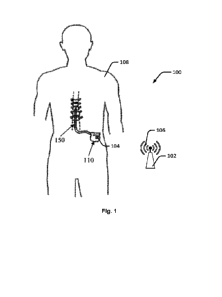
[0043] Fig. 1 illustrates an implanted neuromodulation device and charger;
[0044] Fig. 2 is a schematic illustration of a neuromodulation device;
[0045] Fig. 3 is a flowchart of a method performed by the device of Fig. 2;
[0046] Fig. 4 illustrates exemplary timing sequences according to the method
of Fig. 3;
[0047] Fig. 5 is a schematic illustration of a charging device;
[0048] Fig. 6 is a flowchart of a method performed by the device of Fig. 5;
[0049] Fig. 7 is a flowchart of a method performed by the device of Fig. 2;
[0050] Fig. 8 is a schematic illustration of a neuromodulation device;
[0051] Fig. 9 is a schematic illustration of a neuromodulation device; and
[0052] Fig. 10 is a flowchart of a method performed by the device of Fig. 2.
CA 03191701 2023-02-13
WO 2022/032352
PCT/AU2021/050895
11
Description of Embodiments
[0053] As mentioned above, it is useful to maintain stimuli amplitude within a
therapeutic
range to maintain effective and comfortable neural stimulation. That is, the
stimuli are above
a recruitment threshold and below a comfort threshold. A neural modulation
device can
adjust the amplitude of applied stimulus based on the measurement of a
compound action
potential (CAP) signal that is evoked in response to the stimulus (referred to
as an "ECAP
signal") to keep the stimuli within this therapeutic range. A neural
modulation device
operating in this manner is said to be operating in closed loop mode (i.e.,
with reference to the
use of the ECAP as a type of feedback signal). This may also be referred to as
a closed loop
neural stimulus (CLNS). An ECAP signal typically has a maximum amplitude in
the range of
microvolts, whereas an applied stimulus signal evoking the CAP is typically
several volts.
[0054] Implantable devices that perform CLNS are battery powered and use
intermittent
charging of the battery to remain operational. Fig. 1 illustrates a wireless
charging
system 100 to charge a battery in an implanted neuromodulation device.
Wireless charging
system 100 comprises a charging device (or "charger") 102 to transfer energy
to an energy
storage device 104 (e.g., a battery) of the implanted device 110 using
electromagnetic
radiation 106. The electromagnetic radiation induces a charging current in the
implanted
device 110 which can be used to charge the energy storage device 104.
Implanted device 110
is implanted at a suitable location in a patient 108, such as the lower
abdominal area or
posterior superior gluteal region.
[0055] Charger 102 detects the charge level of the energy storage device 104
as a reflected
impedance. Using this reflected impedance, in response to the charge level of
the energy
storage device 104 reaching a maximum, the charger 102 detects that the energy
storage
device is charged, and automatically ceases transmitting electromagnetic
radiation 106.
[0056] Fig. 2 is a block diagram of implanted device 110 which comprises an
energy storage
device 104 and a telemetry module 114. Energy storage device 104 may be any
suitable
energy storage device, such as a battery or capacitor. Telemetry module 114
transfers power
and/or data between an external device and other modules of device 110. For
example,
telemetry module 114 may receive power from charger 102 to energy storage
device 104.
CA 03191701 2023-02-13
WO 2022/032352
PCT/AU2021/050895
12
Telemetry module 114 may utilise any suitable type of transcutaneous
communication such as
infrared (IR) and other electromagnetic radiation, including capacitive and
inductive transfer.
[0057] Module controller 116 has an associated memory 118 storing patient
settings 120,
control programs 122 and the like. Controller 116 controls a pulse generator
module 124 to
generate stimuli in the form of current pulses in accordance with the patient
settings 120 and
control programs 122. Electrode selection module 126 switches the generated
pulses to the
appropriate electrode(s) of electrode array 150, for delivery of the current
pulse to the tissue
surrounding the selected electrode. Measurement circuitry 128 is configured to
capture
measurements of neural responses sensed at sense electrode(s) of the electrode
array as
selected by electrode selection module 126.
[0058] The neural response is determined by the measurement of an electrical
field
parameter signal by the measurement circuitry 128 components. For example, the
measurement of the electrical field parameter signal may include the
measurement of at least
one of: an evoked neural compound action potential (ECAP); a non-evoked neural
compound
action potential (nECAP); a local field potential (LFP); a slow response, or a
physiological
parameter (such as EMG, ECoG, and EKG). Although the embodiments described
herein
relate to the measurement of an ECAP signal, the skilled addressee will
appreciate that
measurement of any other type of electrical field parameter indicating a
neural response may
be performed alternatively, or in addition.
[0059] The desired magnitude of the charging potential depends on the type of
battery and is
typically in the order of one to five volts. This causes an induced potential
in the
measurement electrodes, which can be several orders of magnitude greater than
the ECAP
signal (microvolts) preventing detection, or accurate measurement, of the ECAP
signal. As a
result, some neuromodulation devices cannot operate to alter the applied
neural stimulus
based on a measurement of the ECAP (i.e., closed loop operation) while the
battery is
charging. Instead, the devices are limited to "open loop" control, where the
amplitude used
for the applied stimulus is not based on a consideration of a dynamically
measured ECAP
signal, which may result in induced stimuli falling outside of the therapeutic
range leading to
unwanted effects such as discomfort for the patient.
CA 03191701 2023-02-13
WO 2022/032352
PCT/AU2021/050895
13
[0060] In order to address this problem, this disclosure provides an
implantable neural
stimulation device, which is also referred to as an "implantable pulse
generator" (IPG)
device, 110 that operates to control the measurement of an evoked neural
compound action
potential (ECAP) signal in response to the charging of the device 110. In the
case that the
ECAP signal is produced in response to the application of a neural stimulus to
a neural
pathway by the implantable device 110, this enables the device 110 to perform
CLNS while
being charged by a charging device (e.g., the charger 102). The implantable
neural stimulus
device 110 comprises a controller 116 having a processor 117 configured to
perform
method 300 of Fig. 3. When performing method 300, processor 117 selectively
operates in
one of a charging mode and a measurement mode.
[0061] At step 302, the processor 117 is in the charging mode and is
configured to receive
electromagnetic radiation 106 from the charger 102. Electromagnetic radiation
106 transfers
energy to implantable device 110 to charge the energy storage device 104 as
described above.
[0062] Processor 117 directs the application of a neural stimulus signal to a
neural pathway.
Specifically, implantable device 110 generates and applies a neural stimulus
signal to the
neural pathway though electrodes 150. The applied stimulus signal evokes a
compound
action potential (ECAP) signal response in the neural pathway which is
measured at a point
along the neural pathway from where the stimulus signal was applied. This ECAP
signal may
be measured and used as a feedback signal to adjust the amplitude of the
neural stimulus
signal.
[0063] Before measuring the ECAP signal corresponding to the application of a
neural
stimulus signal, processor 117 selectively transitions from the charging mode
and to the
measurement mode such that the implantable device 110 does not receive
electromagnetic
radiation 106 from the charger 102 during the measurement of the ECAP. In one
embodiment,
the measurement mode involves the processor 117 signaling to the charging
device 102 to
cease transmission of electromagnetic radiation 106. As a result, charging
device 102
transmits no electromagnetic radiation 106 during the period when implantable
device 110
measures the ECAP signal. The ECAP signal is then detected and measured at a
point along
the neural pathway at step 306. This enables the ECAP signal to be used as a
feedback signal
to adjust the neural stimulus signal (i.e., to perform CLNS). Charging device
102 can resume
transmission of electromagnetic radiation 106 after measurement of the ECAP.
In this case
CA 03191701 2023-02-13
WO 2022/032352
PCT/AU2021/050895
14
the processor 117 selectively transitions back to the charging mode to enable
the charging of
the energy storage device 104.
[0064] In some embodiments, implantable device 110 signals to the charging
device 102 to
cease transmission of the electromagnetic radiation before generating and
applying the neural
stimulus signal. That is, the processor 117 transitions to the measurement
mode prior to
applying the neural stimulus signal. In such embodiments, implantable device
110 comprises
a charging controller and a stimulation module. The stimulation module has an
'enable' input
that is connected to the charging controller. The charging controller clears
the 'enable' signal
to disable stimulation and then signals to the charging device 102 to transmit
electromagnetic
radiation. After a period of time, such as the calculated time between
stimulation pulses, the
charging controller signals to charging device 102 to cease transmission of
the
electromagnetic radiation and sets the 'enable' signal to enable stimulation.
[0065] In some implementations, after signalling to the charging device 102 to
cease
transmission, implantable device 110 waits for an acknowledgement from the
charging device
102 or detects the actual ceasing of the electromagnetic radiation before
enabling stimulation
and subsequent measurement of the ECAP signal.
[0066] The timing sequence of these processes are shown in Figs. 4A to 4E.
Fig. 4A is the
output of charger 102, while Figs. 4B, C and D take place in device 110.
[0067] At an initial time ti, charger 102 is transmitting electromagnetic
radiation 106 as
indicated by transmission signal 402. Transmission signal 402 is illustrated
as a rectangular
section because the electromagnetic radiation is typically a high frequency
alternating current
(AC) signal with a frequency typically between 250KHz and 400KHz, though
frequencies as
high as 5MHz have been used. At this time, processor 117 is operating in
charging mode and
performing step 302 of method 300. At a later time, t2, processor 117 applies
a stimulus
signal 404 and measures the evoked CAP signal 406 at a later time, t3. As
discussed above,
CAP signal 406 is used as feedback to adjust the amplitude of future stimulus
waveforms 404'. At a time t4, which is prior to t3, processor 117 transmits an
interrupt
signal 408 to charger 102 to cease transmission of electromagnetic radiation
as indicated by
transmission voltage dropping to zero at 402'(i.e., during the measurement
mode).
CA 03191701 2023-02-13
WO 2022/032352
PCT/AU2021/050895
[0068] Figs. 4C and 4D illustrate stimulus signal 404 and ECAP signal 406 as
having no
temporal overlap. However, in practice, stimulus signal 404 and ECAP signal
406 may
overlap depending on the physical arrangement of the electrodes and
propagation velocity of
stimulus signal 404 along the nerve fibres. In some embodiments, the ECAP
signal 406 is
measured at the same time that stimulus signal 404 is applied. That is, t2 and
t3 occur at the
same time.
[0069] As charger 102 is not transmitting electromagnetic radiation at time t3
when ECAP
signal 406 is being measured, implantable device 110 can detect and accurately
measure
ECAP signal 406 to use it as a feedback signal.
[0070] Figs. 4A to 4D illustrate an implementation of method 300 when
interrupt signal 408
is transmitted not only before ECAP signal 406 is measured, but also before
stimulus
signal 404 is applied to the neural pathway. That is, t4 is prior to t3 and
t2.
[0071] At some later time, ts, charger 102 recommences transmission of
electromagnetic
radiation 106 to continue charging of the energy storage device 104. In some
embodiments,
processor 117 transmits a recommence signal (not shown) after the ECAP signal
406 has been
measured, causing charger 102 to recommence transmission of electromagnetic
radiation 106.
[0072] In other embodiments, the neural stimulus signal is applied during the
transmission
of the electromagnetic radiation (i.e., during the charging mode) and the
processor 117
transitions from the charging mode to the measurement mode after the
application of the
stimulus signal, and before the measuring of the corresponding ECAP signal. As
before,
charging device 102 only recommences transmission of electromagnetic radiation
106 after
device 110 has measured the ECAP signal. This is illustrated by the interrupt
signal 409 of the
implantable device 110 shown in Fig. 4B, and the transmission signal output
410 of the
charger 102 shown in Fig. 4E (both signals being depicted in dashed lines). In
this
embodiment, the processor 117 transmits the interrupt signal 409 to charger
102 at a time t4'
(shown only in Figs. 4B and 4E) to cease transmission of electromagnetic
radiation 106
according to the transmission signal 410. Time t4 occurs after time t2 , which
is when the
processor 117 applies the stimulus signal 404, but prior to time t3 when the
processor 117
measures the evoked CAP signal 406.
CA 03191701 2023-02-13
WO 2022/032352
PCT/AU2021/050895
16
[0073] In some embodiments, processor 117 continuously transmits interrupt
signal 408 for
a period of time required to both apply stimulus signal 404 and measure
corresponding ECAP
signal 406. This period is referred to as a stimulation-recording period. At
the end of the
stimulation-recording period, processor 117 ceases transmission of interrupt
signal 408
causing charger 102 to recommence transmission of electromagnetic radiation
106. In the
example illustrated in Figs. 4A to 4E, the stimulation-recording period is two
milliseconds.
[0074] In some embodiments, charger 102 automatically recommences transmission
of
electromagnetic radiation 106 after a predetermined period from receiving the
first interrupt
signal that signals the ceasing of the transmission. The predetermined time
period may be
stored on charger 102 or communicated to charger 102 from implantable device
110, either
through interrupt signal 408 or through a separate communication.
[0075] It will be appreciated that interrupt signal 408 can take many forms.
In one example,
interrupt signal 408 is a reflected impedance which is indicative of a charged
energy storage
device. That is, processor 117 simulates an electrical load on telemetry
module 114 which is
equivalent to the electrical load that would be experienced if the energy
storage device 104
were fully charged. This reflected impedance is detected by charger 102,
causing charger 102
to cease transmission of electromagnetic radiation 106.
[0076] An advantage of using the reflected impedance as interrupt signal 408
is that there
would be no requirement to modify charger 102 if such a charger were already
in use.
[0077] In another example, interrupt signal 408 is a wireless electromagnetic
radio
frequency signal. For example it may be a radio frequency signal within a
medical implant
communication service (MICS) band.
[0078] Processor 117 of device 110 may periodically operate in the measurement
mode to
provide a prolonged therapeutic effect to patient 108. In the example
illustrated in Figs. 4A to
4D, processor 117 periodically alternates between charging mode and
measurement mode
with a period of twenty milliseconds (which corresponds to a frequency of
fifty hertz). In this
case, processor 117 operates in measurement mode for a stimulation-recording
period of two
milliseconds and then operates in charging mode for the remainder of the
twenty millisecond
CA 03191701 2023-02-13
WO 2022/032352
PCT/AU2021/050895
17
period (i.e. eighteen milliseconds). There is no overlap between the
measurement mode and
the charging mode.
[0079] In other embodiments, the processor 117 may perform one or more adhoc
transitions
to the measurement mode. These transitions may occur at random instances, such
as, for
example, whenever the charger 102 begins actively transferring electromagnetic
radiation 106
to the implantable device 110. In some embodiments, the 117 transitions may
occur when the
implantable device 110 is directed to measure an electrical parameter
representing a neural
response, such as an ECAP, a non-evoked CAP, a local field potential (LFP), a
slow response,
a physiological parameter (such as EMG, ECoG, and EKG), or a like parameter.
[0080] In some implementations, processor 117 monitors a charge level of the
energy
storage device 104. While the charge level is above a predetermined threshold,
processor 117
continuously generates interrupt signal 408. In this case, if device 110 comes
into operational
range of a charger 102, the charger will not transmit electromagnetic
radiation as it will detect
interrupt signal 408. When the charge level drops below the predetermined
threshold,
processor 117 will execute method 300 as described above, enabling the energy
storage
device 104 to be charged by the charger 102 while also enabling the adjustment
of the
stimulus signal based on a measured ECAP signal.
[0081] In some implementations, processor 117 executes method 300 continuously
enabling
the energy storage device 104 to charge each time device 110 moves within
operational range
of charger 102.
[0082] The instructions for method 300 are stored in control programs 122 and
are
embodied in a software program written in a programming language such as C++
or Java.
The resulting source code is then compiled and stored as computer executable
instructions.
[0083] Fig. 5 is a schematic illustration of charging device 102 which
comprises a controller
502, with associated memory 504 and an antenna 506. Controller 502 comprises
processor 508 for executing instructions stored in charging control program
510 on
memory 504. Antenna 506 is configured to transmit electromagnetic radiation
106 to
implantable device 110. Charging control program 510 comprises instructions to
perform
method 600 which is illustrated in Fig. 6.
CA 03191701 2023-02-13
WO 2022/032352
PCT/AU2021/050895
18
[0084] At step 602, controller 502 controls charging device 102 to transmit
electromagnetic
radiation to implantable device 110. As mentioned above, charger 102 transfers
energy to the
energy storage device 104. An interrupt signal 408 is received at step 604
causing
controller 502 to execute step 606 by ceasing transmission of electromagnetic
radiation 102.
[0085] In some embodiments, method 600 is executed in a loop such that step
602 is
executed again after step 606.
[0086] In some embodiments, method 600 loops back to step 602 when interrupt
signal 408
is no longer received. That is, controller 502 executes step 606 while
interrupt signal 408 is
received and when interrupt signal 408 is not received it executes step 602.
[0087] In some embodiments, method 600 loops back to step 602 after a
predetermined
period of time of ceasing transmission. The predetermined period of time may
be stored in
charging control program 510. Alternatively, the predetermined period of time
may be
derivable from interrupt signal 408 or received as a separate communication
from implantable
device 110.
[0088] In some embodiments, method 600 loops back to step 602 when a separate
recommence signal (not shown) is received.
[0089] In some embodiments, charging device 102 is configured to transmit
electrical
energy (i.e., electromagnetic radiation 106) according to a pre-determined
duty cycle and
predetermined frequency. That is, charger 102 is configured to transition from
an active state
in a first part of a charging cycle to a standby state in a second part of a
charging cycle
according to a predetermined duty cycle. In the active state, charger 102
transmits
electromagnetic radiation to the implantable device 110 and in the standby
state charger 102
does not transmit electromagnetic radiation to the implantable device. The
duty cycle is
defined by a relationship between the temporal duration of the first part of
the charging cycle
and the temporal duration of the second part of the charging cycle. The first
and second parts
of the charging cycle are repeated at the predetermined frequency.
[0090] In some implementations, the charger 102 performs the transmission of
electrical
energy according to the pre-determined duty cycle and frequency without
receiving an
CA 03191701 2023-02-13
WO 2022/032352
PCT/AU2021/050895
19
interrupt signal. That is, with reference to method 600, the charger 102 may
be configured to
transition back and forth between the active state (at step 602), and the
standby state (at step
606), without receiving an interrupt signal from the implantable device 110.
Direct transition
of the charger 102 from step 602 to 606, and the corresponding reverse
transition, are shown
as dashed lines in Fig. 6.
[0091] In some embodiments, the charger 102 is configured to initiate the
transmission of
electrical energy according to the pre-determined duty cycle and frequency
automatically on
the detection of the implantable device 110. The charger 102 includes
detection circuitry
configured to enable the detection of the implantable device 110. For example,
the charger
102 may sense the presence of the implantable device 110 via a change in the
reflective
impedance detected within a coil, or similar component, of the charger 102 and
initiate
charging according to the pre-determined duty cycle.
[0092] Although, the charger 102 is not required to receive an interrupt
signal to commence
transmission of electrical energy according to the pre-determined duty cycle
and frequency,
the charger 102 may still receive such an interrupt signal. In some
implementations, the
charger 102 is configured to respond to the received interrupt signal to alter
the transmission
of electrical energy in a pre-specified manner. For example, the charger 102
may be
configured to respond by: ceasing transmission of the electrical energy
entirely (e.g., invoking
a turn-off' function); commencing a pre-determined cool-off period in which
transmission of
electrical energy is immediately ceased and then resumed on termination of the
cool-off
period according to the pre-determined duty cycle; advancing to the second
part of the current
charging cycle; and/or resetting the duty cycle. For the purposes of
discussion, when
operating in this embodiment the charger 102 will be referred to as the master
charger 102.
[0093] In some implementations, the predetermined frequency and duty cycle is
configurable based on a received configuration signal. For example, the duty
cycle and
frequency of the charger may be transmitted to it from the implantable device
110, or from a
remote control used by the patient to control the implantable device, or, the
frequency and
duty cycle may be established in a clinic by a clinician.
[0094] In some embodiments, implantable device 110 is configured to receive
electromagnetic radiation from charger 102 discussed above. Processor 117
selectively
CA 03191701 2023-02-13
WO 2022/032352
PCT/AU2021/050895
operates in one of a charging mode and a measurement mode based on whether the
charger
102 is in the first part of the charging cycle or the second part of the
charging cycle.
Processor 117 detects the first and second parts of the charging cycle in
response to receiving
electromagnetic radiation and operates in the charging mode during the first
part of the
charging cycle. As before, when in the charging mode, electromagnetic
radiation is received
from charging device 102 to charge the energy storage device 104.
[0095] In some embodiments, processor 117 determines the predetermined
frequency and
duty cycle of master charger 102 by monitoring the electromagnetic radiation
from master
charger 102. In one embodiment, processor 117 measures the time between
successive first
parts of the charge cycle to determine the predetermined frequency (being the
inverse of the
measured time period) and measures the duration of the first part of the
charge cycle to
determine the predetermined duty cycle.
[0096] Processor 117 can be configured to periodically perform stimulation
cycles at the
predetermined frequency such that the stimulation cycles are synchronised with
the second
part of the charge cycle. In each stimulation cycle, processor 117 applies a
neural stimulus to
the neural pathway and measures a ECAP response signal. The result of this is
that
processor 117 performs a stimulation cycle each time master charger 102 ceases
transmission
of electromagnetic radiation.
[0097] In some embodiments, processor 117 does not perform a complete
stimulation cycle
during each second part of the charge cycle. Rather, processor 117 is
configured to perform
an incomplete stimulation cycle by only applying a neural stimulus during the
second part of
the charge cycle and not measuring an evoked neural action potential.
Processor 117 may
periodically perform complete stimulation cycles to adjust the level of
stimulation. That is,
processor 117 may perform incomplete stimulation cycles interspersed with
complete
stimulation cycles. As a result of processor 117 only occasionally performing
a complete
stimulation cycle, the energy storage device 104 is able to charge faster as
processor 117
consumes less energy when performing incomplete stimulation cycles.
[0098] Using the detected electromagnetic radiation, processor 117 is able to
predict when
master charger 102 will be in the second part of the charge cycle as the
second part of the
charge cycle is also repeated at the predetermined frequency. Synchronising
the stimulation
CA 03191701 2023-02-13
WO 2022/032352
PCT/AU2021/050895
21
cycles is then a matter of processor 117 performing the stimulation cycles at
the
predetermined frequency and with a phase off-set that allows the stimulation
cycles to fall
within the second part of the charge cycle. The phase off-set will be
determined by the
predetermined duty cycle and is effectively a timing off-set.
[0099] For example, processor 117 determines a start of each coming charge
cycle using the
detected first part of the charge cycle and the measured time between
successive starts. A
phase delay, or timing off-set, equal to the duration of the first part of the
charge cycle is then
be added to these times to yield predicted times for the second parts of the
charge cycle.
[0100] In some embodiments, the phase delay is only calculated once and the
stimulation
cycles are then performed at the predetermined frequency. In other
embodiments, the phase
off-set is periodically determined to ensure that the stimulation cycles
remain synchronised
with the second part of the charge cycle.
[0101] In some embodiments, the measurements of the ECAP are used to determine
the
upper and lower stimulation thresholds rather than in a feedback loop to
maintain the stimulus
between the respective threshold levels, as for the embodiments described
above. Determining
the relevant thresholds enables the delivery of stimulation at an intensity
that does not result
in the detection of an ECAP response signal.
[0102] For example, the ECAP measurements may be used to determine the minimum
level
of stimulation required to evoke a detectable response (i.e., the ECAP may be
recorded for a
level of stimulation, and the implanted device configured to reduce the
stimulation level until
the ECAP is no longer detectable). Applying stimulation at an intensity below
this value can
be considered as subthreshold stimulation. Subthreshold stimulation may be
performed
without measuring a corresponding evoked compound action potential. Rather, in
this
embodiment, the processor 117 is configured to only apply a neural stimulus to
the neural
pathway which may occur when the implantable device 110 is being charged by
the charger
102 (i.e., in the charging mode).
[0103] In some embodiments, when operating in either the charging or
measurement
modes, processor 117 does not apply a neural stimulus to the neural pathway.
Rather,
processor 117 is configured to only measure non-evoked neural activity in
measurement
CA 03191701 2023-02-13
WO 2022/032352
PCT/AU2021/050895
22
mode. That is, the processor 117 may be configured to detect electrical field
signal parameters
that are not produced or evoked by the implantable device 110 via the
measurement of non-
evoked neural activity. For example, the signal passing along the neural
pathway may
indicate that the patients bladder is full. A measurement of this signal may
be taken during
measurement mode, when charger 102 is not transmitting electromagnetic
radiation to
device 110.
[0104] The functionality of the previously described embodiments, in which
processor 117
selectively transitions between operating in the charging mode and the
measurement mode, is
performed by the implantable device 110 as part of a "smart charging"
operational routine. In
some embodiments the implantable device 110 is configured to transition
between various
operational routines, including: the smart charging operational routine; a
conventional
feedback based operational routine, where the stimulus signal is altered based
on the ECAP
measurements without compensating for any charging activity (e.g., when the
implantable
device 110 operates without charger 102); and a static stimulus operational
routine where a
neural stimulus is applied to a neural pathway without any dynamic adjustment
of the neural
stimulus signal (irrespective of whether measurement of a corresponding neural
compound
action potential response evoked by the applied stimulus is performed). In
some cases, the
implantable device 110 may measure an electrical parameter associated with the
tissue of the
patient 108 whilst applying static stimulus. The implantable device 110 may
cease the
application of static stimulus, measure the electrical field parameter, and
then resume the
application of the static stimulus. In this case, the measured electrical
field parameter is not
used to adjust or alter the neural stimulus.
[0105] In some embodiments, the implantable device 110 is configured to detect
the
presence of the charger 102 within a charging proximity of the implantable
device 110, and to
automatically transition to the smart charging operational routine in response
to the detection.
That is, the implantable device 110 may transition between operational
routines to optimize
its function depending on the environment of its operation, and whether the
implantable
device 110 is receiving electromagnetic (EM) radiation 106 from an emitting
device (i.e.,
either the charger 102, or another device).
[0106] For example, it may be desirable for the implantable device 110 to
function in a
static stimulus operational routine when the charger 102 is unavailable and
when the
CA 03191701 2023-02-13
WO 2022/032352
PCT/AU2021/050895
23
implantable device 110 is subject to electromagnetic radiation 106 in the form
of noise
generated by another emitting device (e.g., an arc welder). In this situation,
attempting to
measure the ECAP response signal, such as for the purpose of performing
feedback based
control of the applied stimulus, may lead to a worse outcome than the static
approach (i.e.,
where the inaccurate measurement of the evoked CAP signal results in
maladjustment of the
intensity of the induced stimuli).
[0107] In other situations, such as when the implantable device 110 does not
receive
electromagnetic radiation from the charger 102, or any other emitting device,
an operational
routine without stimulation and charging cycle functionality may be
advantageous (e.g., since
the measurement of the ECAP is not temporally restricted to occur within any
particular
period outside of a charging cycle).
[0108] Fig. 7 illustrates a process 700 performed by the implantable device
110 for
automatically transitioning to a smart charging operational routine on
detection of the charger
102. At step 702, the implantable device 110 detects the presence of an
emitting device within
a charging distance of the implantable device 110. The charging distance is
the maximum
distance at which emitting device is capable of inducing a charging current in
the implanted
device 110, and therefore a potential in the measurement electrodes such as to
affect the
detection of the CAP signal (as described above). The charging distance is
variable depending
on the properties of the implantable and emitting devices.
[0109] Fig. 8 illustrates an exemplary configuration of the implantable device
110 including:
a charging coil 130 configured to convert electromagnetic radiation 106
received from
charger 102 to a charging current in the implanted device 110; and a sensor
132 associated
with the charging coil 130. In some embodiments, the charging coil 130 is
formed from a Litz
wire, or other type of multi-strand wire, with at least 100 strands of wire
per cable. The sensor
132 is configured to detect the electromagnetic radiation 106, and therefore
the presence of
the charger 102 or other emitting device, within the charging distance. For
example, the
sensor 132 may be a component that senses the voltage and/or current induced
by the EM
radiation 106 from the charger 102.
[0110] In some embodiments, the sensor 132 is electrically connected to the
coil 130 and is
configured to measure the charge induced by EM radiation 106. In other
embodiments, the
CA 03191701 2023-02-13
WO 2022/032352
PCT/AU2021/050895
24
sensor 132 may be an independent detection component physically located in the
vicinity of
the coil 130. In this case, the intensity of the EM radiation incident on the
sensor 132
corresponds to that of the coil 130 for the purpose of enabling the sensor 132
to determine the
proximity of the charger 102 to the device 110 . The sensor 132 is configured
to output a
detection signal based on the intensity of the incident EM radiation 106. The
processor 117
determines a positive detection of the charger 102 in response to a value of
the detection
signal exceeding a predetermined detection threshold value.
[0111] In another exemplary configuration, as shown by Fig. 9, the controller
116 of the
implantable device 110 includes an amplifier 134 configured to sense noise
resulting from the
EM radiation 106. The amplifier is a differential amplifier, as described in
US9386934 which
is incorporated herein by reference. The amplifier 134 senses a noise
associated with the
electromagnetic radiation 106 received from the emitting device (i.e., the
charger 102 as
depicted in Fig. 8). The processor 117 receives an output noise signal from
the amplifier 134
and detects the presence of the emitting device (e.g., charger 102) based at
least in part on the
noise signal. That is, the EM sensing amplifier 134 detects the proximity of
the charger 102,
or other emitting device, to the implantable device 110 through the noise
resulting from the
incident EM radiation 106 thereby providing an alternative to measuring the
induced charge.
[0112] Referring back to Fig. 7, at steps 704 and 706 the implantable device
110 verifies
whether the emitting device (detected in step 702) is the charger 102.
Specifically, the
implantable device 110 is configured to detect any emitting device acting as a
source of EM
radiation 106, such as for example via the sensor 132 described above. In some
embodiments,
verification of the charger 102 is based on the transmission of at least one
interrupt signal to
the emitting device, and the detection of a corresponding response of the
emitting device that
indicates whether the emitting device is the charger 102 or otherwise.
[0113] At step 704, the processor 117 transmits one or more interrupt signals
to the emitting
device. The form of the interrupt signal and its transmission may vary
according to different
embodiments of the device 110. For example, in some embodiments the processor
117
continuously transmits a single interrupt signal for a predetermined period of
time. In other
embodiments, the processor 117 transmits each interrupt signal as a short
duration pulse
signal over the predetermined period. The predetermined period during which
the processor
117 transmits interrupt signal(s) is referred to as the interrupt period.
CA 03191701 2023-02-13
WO 2022/032352
PCT/AU2021/050895
[0114] At step 706, the processor 117 is configured to detect a response of
the emitting
device to the one or more interrupt signals. The response that enables the
processor 117 to
positively verify the emitting device as the charger 102 is referred to as an
acknowledgment
response. In the described embodiments, the acknowledgment response involves
the ceasing
of the transmission of the EM radiation 106 by the emitting device. That is,
positive
verification of the emitting device as the charger 102 is achieved when the
transmission of an
interrupt signal causes the ceasing of the transmission EM radiation 106 by
the emitting
device (i.e., as an acknowledgment response). Processor 117 detects the
ceasing of the
transmission of the EM radiation 106, as a response to the interrupt signal of
the implantable
device 110, in the same manner as for the embodiments described above.
[0115] In some embodiments, the acknowledgment response also includes the
recommencement of transmission of electromagnetic radiation 106 by the
emitting device.
For example, the acknowledgment response may involve the emitting device
ceasing
transmitting EM radiation 106, and then recommencing transmission according to
a pre-
determined duty cycle and predetermined frequency. Following the transmission
of the one or
more interrupt signals, the processor 117 detects the corresponding pattern
associated with the
transmission of EM radiation 106 according to the pre-determined duty cycle in
which
electrical energy transmission occurs intermittently with periodic repetition
(as discussed
above), and subsequently verifies the emitting device as the charger 102. In
some
embodiments, the processor 117 is configured to utilize a detection of the
recommencement
of transmission of EM radiation 106, following an initial ceasing of the
transmission, within a
single acknowledgment period to distinguish between the absence of any
emitting device, and
the presence of the charger 102 operating according to a predetermined duty
cycle.
[0116] In some embodiments, the period in which the processor 117 determines
the
existence of the acknowledgment response, or otherwise, is referred to as the
acknowledgment period. The acknowledgment period may commence following the
interrupt
period, such as for example when the interrupt signal is a single continuous
signal.
Alternatively, in other configurations the acknowledgment period may overlap
with the
interrupt period.
[0117] At step 708, in response to the processor 117 positively verifying the
emitting device
as the charging device 102, the processor 117 transitions the implantable
device 110 from any
CA 03191701 2023-02-13
WO 2022/032352
PCT/AU2021/050895
26
other operational routine to the smart charging operational routine (i.e.,
such that the
processor 117 operates according to the measurement and charging modes
described herein).
[0118] In some embodiments, the verification of the emitting device as the
charging device
is performed without the transmission of interrupt signals by the implantable
device 110. In
some embodiments where the controller 116 includes the sensing amplifier 134,
the processor
117 is configured to determine the noise as being associated with the charging
device 102.
That is, the processor 117 maintains a noise profile indicative of the EM
noise characteristics
produced by the charger 102 when located within the charging distance of the
device 110.
[0119] For example, the noise profile may be in the form of a numerical or
statistical model
defined by one or more parameters of a noise signal feature space. The noise
profile may be
created by classification and/or model training operations performed on an
external computer
system, and by subsequently loading the output profile into the memory 118 of
controller 116.
The processor 117 is configured to compare feature values of the noise signal
output by the
amplifier 134 (i.e., the noise signature of the emitting device) to
corresponding parameters of
the noise profile to determine whether the noise signature is recognized as
being of the
charger 102 (i.e., as represented by the noise profile). Identification of the
charger 102 via
noise signature recognition is advantageous in that the processor 117 does not
need to rely on
the proper reception of interrupt signals by the emitting device, and need not
wait for the
emitting device to provide the acknowledgment response to achieve positive
verification.
[0120] The implantable device 110 is also configured to automatically
transition to other
operational routines in response to determining that an emitting device is not
the charger 102.
For example, Fig. 10 illustrates a process 1000 performed by the implantable
device 110 for
automatically switching to an static stimulus signal based routine. At steps
1002 and 1004, the
processor 117 detects the presence of an emitting device within a charging
distance of the
implantable device 110, and transmits one or more interrupt signals to the
emitting device (as
described above for steps 702 and 704).
[0121] At step 1006, the processor 117 attempts to detect a response of the
emitting device
to the one or more interrupt signals. That is, the processor 117 transmits the
one or more
interrupt signals to the emitting device during a first interrupt period, and
then attempts to
determine an acknowledgment response during a corresponding first
acknowledgment period.
CA 03191701 2023-02-13
WO 2022/032352
PCT/AU2021/050895
27
In some embodiments, the first acknowledgment period is of a predetermined
length (e.g.,
between 20 and 1000ms) and may commence directly following the interrupt
period. In the
exemplary process of Fig. 10, the first acknowledgment period terminates
without the
processor 117 determining the existence of the acknowledgment response of the
charger 102
(i.e., involving the ceasing of the transmission EM radiation 106 by the
emitting device). That
is, in this case the processor 117 detects an absence of the acknowledgment
response of the
emitting device within the first acknowledgment period.
[0122] At step 1008, in response to detecting the absence of the
acknowledgment response
within the first acknowledgment period, the processor 117 causes the
implantable device 110
to transition, from any other operational routine, to the static stimulus
operational routine
where the stimulus signal is not modified in response to a measurement of the
ECAP signal.
[0123] In some embodiments, when the implantable device 110 is in the static
stimulus
operational routine the processor 117 is prevented from measuring the ECAP
signal
associated with any application of a neural stimulus signal. That is, the
processor 117 is
configured to apply a neural stimulus to one or more neural pathways without a
corresponding
measurement of an ECAP resulting from the applied stimulus. That is, the
processor 117 has
determined that the emitting device is not the charger 102, and prevents the
implantable
device 110 from measuring ECAP signals due to the presence of the EM radiation
106. This
prevents noise associated with the EM radiation from compromising the
measurement and
subsequent use of an evoked CAP signal (as may occur in a conventional closed
loop control
routine).
[0124] In some other embodiments, when the implantable device 110 is in the
static
stimulus operational routine the processor 117 may measure the ECAP signal
associated with
the application of a neural stimulus signal, but is prevented from altering
the neural stimulus
signal based on the ECAP measurement (i.e., due to the likelihood of the noise
associated
with the EM radiation compromising the measurement).
[0125] In some embodiments, the implantable device 110 is configured to
maintain the static
stimulus operational routine for a predetermined period. This is referred to
as the back-off
period. Following termination of the back-off period, the processor 117 may
repeat the
interrupt transmission and acknowledgment response cycle (as indicated by the
dashed line in
CA 03191701 2023-02-13
WO 2022/032352
PCT/AU2021/050895
28
Fig. 10). That is, the processor 117 retransmits the one or more interrupt
signals to the
emitting device during a second interrupt period, and attempts to determine an
acknowledgment response during a corresponding second acknowledgment period.
If the
processor 117 detects the acknowledgment response during the second
acknowledgment
period (i.e., at step 1010), then the emitting device is positively verified
as the charger 102. In
this case, the processor 117 causes the implantable device 110 to transition
from the static
stimulus operational routine to the smart charging operational routine (i.e.,
at step 1012) in the
same manner as for the embodiments described above. Otherwise, the processor
117 initiates
a further back-off period.
[0126] In some embodiments, the processor 117 is configured to repeat the
interrupt
transmission and acknowledgment response cycle until the charger 102 is
detected, enabling
the automatic transition to the smart charging operational routine, as
described above. The
processor 117 is configured to control the durations and commencement times of
the
respective interrupt, acknowledgment, and back-off periods of each cycle to
facilitate the
detection of the charger 102. For example, the acknowledgment period may be
set to
commence directly after the interrupt period, and with a duration set as equal
to or greater
than the duration of the charging cycle of the charger 102. This enables the
detection of any
ceasing of the transmission of electromagnetic radiation by the charger 102
within the
corresponding acknowledgment period (since at least a portion of the second
part of the
charging cycle will fall within the acknowledgment period).
[0127] It will be appreciated by persons skilled in the art that numerous
variations and/or
modifications may be made to the above-described embodiments, without
departing from the
broad general scope of the present disclosure. The present embodiments are,
therefore, to be
considered in all respects as illustrative and not restrictive.
[0128] It should be understood that the techniques of the present disclosure
might be
implemented using a variety of technologies. For example, the methods
described herein may
be implemented by a series of computer executable instructions residing on a
suitable
computer readable medium. Suitable computer readable media may include
volatile (e.g.
RAM) and/or non-volatile (e.g. ROM, disk) memory, carrier waves and
transmission media.
CA 03191701 2023-02-13
WO 2022/032352
PCT/AU2021/050895
29
[0129] It should also be understood that, unless specifically stated otherwise
as apparent
from the following discussion, it is appreciated that throughout the
description, discussions
utilizing terms such as "estimating" or "processing" or "computing" or
"calculating",
"optimizing" or "determining" or "displaying" or "maximising" or the like,
refer to the action
and processes of a computer system, or similar electronic computing device,
that processes
and transforms data represented as physical (electronic) quantities within the
computer
system's registers and memories into other data similarly represented as
physical quantities
within the computer system memories or registers or other such information
storage,
transmission or display devices.
[0130] The present embodiments are, therefore, to be considered in all
respects as
illustrative and not restrictive.