Note: Descriptions are shown in the official language in which they were submitted.
CA 03193133 2023-02-24
- 1 -
Description
Optical waveguide for a magneto-optical current sensor
The invention relates to an optical waveguide for a
magnetooptical current sensor and a magnetooptical current
sensor having such an optical waveguide.
A magnetooptical current sensor having an optical waveguide is
understood here as an optical measuring device for measuring an
electrical current in a current conductor, in which light is
guided through the optical waveguide and is changed in its
optical properties in the optical waveguide by a magnetic field
generated by the current. For example, a magnetooptical current
sensor is based on the magnetooptical Faraday effect. The
Faraday effect is understood as the rotation of the polarization
direction of a linearly polarized electromagnetic wave in a
medium by a magnetic field in parallel to the propagation
direction of the wave. The rotation of the polarization
direction is proportional in this case to the magnetic flux
density of the magnetic field.
In a magnetooptical current sensor based on the Faraday effect,
linearly polarized light is conducted through an optical
waveguide arranged in the vicinity of the current conductor,
which displays the Faraday effect. The magnetic field generated
by the current in the current conductor causes a rotation of the
polarization direction of the light in the optical waveguide.
Since the magnetic flux density of the magnetic field in the
optical waveguide is dependent on the amperage of the current
in the current conductor, the amperage may be measured in that
the rotation of the polarization direction of the light in the
optical waveguide is detected. To detect the rotation of the
polarization direction, the light output by the optical
waveguide is guided, for example, through an output-side
Date recue/Date received 2023-02-24
CA 03193133 2023-02-24
- 2 -
polarizer and a light intensity of the light transmitted by the
polarizer is detected.
The light intensity of the light which is coupled into the
optical waveguide of a magnetooptical current sensor is limited
due to optical properties of the optical waveguide and/or the
light source used, however. Furthermore, the light intensity of
the light which is output by the optical waveguide is reduced
in comparison to the light intensity of the light coupled into
the optical waveguide by scattering, absorption, and reflection
of light. The light intensity of the light output by the optical
waveguide is determined, for example, using a photodiode.
Photodiodes have a base noise, which is composed of greatly
varying noise sources. A very low light intensity output by the
optical waveguide results in a low signal-to-noise ratio of the
measurement signal and therefore limits the accuracy of the
measurement of the light intensity.
An increase of the light intensity of the light coupled into the
optical waveguide by using a brighter light source is often not
possible or not advantageous for various reasons. For example,
the light intensity can be increased by using a suitable
semiconductor laser as a light source. However, the vibration
sensitivity of the magnetooptical current sensor increases
strongly here due to the increased coherence length of the light.
Limits are also placed on an improvement of the signal-to-noise
ratio of the measurement signal by corresponding filtering of
the measurement signal, which reduces the bandwidth of the
resulting measurement signal, since the reduction of the
bandwidth reduces the time resolution of the measurement signal.
The invention is based on the object of increasing the light
intensity of the light output by an optical waveguide of a
magnetooptical current sensor.
Date recue/Date received 2023-02-24
CA 03193133 2023-02-24
- 3 -
The object is achieved according to the invention by an optical
waveguide having the features of claim 1 and a magnetooptical
current sensor having the features of claim 10.
Advantageous embodiments of the invention are the subject matter
of the dependent claims.
An optical waveguide according to the invention for a
magnetooptical current sensor comprises a first end face,
through which light can be coupled into the optical waveguide,
and a second end face, through which light can be decoupled from
the optical waveguide, wherein at least one of the two end faces
has an antireflective coating.
The reflection of light at one end face of the optical waveguide
according to the invention is reduced by an antireflective
coating and the transmission of light through the end face is
thus increased. If the end face, through which light is coupled
into the optical waveguide, is provided with an antireflective
coating, the light intensity of the light coupled into the
optical waveguide can be increased by approximately 10 to 20%
in relation to an embodiment of the optical waveguide without
this antireflective coating. If the end face, through which
light is decoupled from the optical waveguide, is provided with
an antireflective coating, the light intensity of the light
decoupled from the optical waveguide can be increased by
approximately 10 to 20% in relation to an embodiment of the
optical waveguide without this antireflective coating.
Furthermore, an antireflective coating of the end face through
which light is decoupled from the optical waveguide also
advantageously reduces reflections of light at this end face,
which reflect light back into the optical waveguide.
One embodiment of the optical waveguide according to the
invention has at least one antireflective layer, which is
arranged between two optical waveguide sections having indices
Date recue/Date received 2023-02-24
CA 03193133 2023-02-24
- 4 -
of refraction different from one another. At a boundary layer
between two optical waveguide sections having indices of
refraction different from one another, a part of the light which
is incident on the boundary layer is reflected. The transmission
of light through the boundary layer and the light intensity of
the light output by the optical waveguide are thus reduced. In
addition, light is reflected back in the optical waveguide in
the direction opposite to a provided passage direction. The
antireflective layer between the two optical waveguide sections
advantageously reduces the reflections of light between the
optical waveguide sections and thus increases the light
intensity of the light output by the optical waveguide in
relation to an embodiment of the optical waveguide without the
antireflective layer.
In a further embodiment of the optical waveguide according to
the invention, the optical waveguide is manufactured at least
in sections from glass, for example from optical flint glass.
If the optical waveguide has optical waveguide sections which
are manufactured from different glasses having indices of
refraction different from one another, according to the above-
mentioned embodiment of the optical waveguide according to the
invention, an antireflective layer is preferably arranged
between two adjacent such optical waveguide sections.
Alternatively or additionally, an adhesive layer can be arranged
between two such optical waveguide sections, by which the two
optical waveguide sections are adhesively bonded to one another,
wherein the adhesive layer has an index of refraction which is
between the indices of refraction of the two optical waveguide
sections. The manufacturing of the optical waveguide from glass
has the advantage over the use of fiber-optic optical
waveguides, for example, that costly optical fibers do not have
to be used as the optical waveguide, which maintain a linear
polarization of the light. An adhesive layer between two optical
waveguide sections made of glasses having indices of refraction
different from one another also advantageously reduces
Date recue/Date received 2023-02-24
CA 03193133 2023-02-24
- 5 -
reflections at a boundary layer between the optical waveguide
sections if the adhesive layer has an index of refraction which
is between the indices of refraction of the two optical waveguide
sections.
In a further embodiment of the optical waveguide according to
the invention, the optical waveguide is designed at least in
sections as a fiber-optic optical waveguide. If the optical
waveguide has optical waveguide sections which are designed as
fiber-optic optical waveguides different from one another having
indices of refraction different from one another, according to
the above-mentioned embodiment of the optical waveguide
according to the invention, an antireflective layer is
preferably arranged between two adjacent such optical waveguide
sections. An end face which has an antireflective coating is in
the case of an optical waveguide formed by one or more fiber-
optic optical waveguides, for example, an end face of a fiber-
optic optical waveguide or an end face of a ferrule of a fiber-
optic optical waveguide.
A magnetooptical current sensor according to the invention for
detecting an amperage of an electrical current in a current
conductor comprises at least one optical waveguide according to
the invention arranged in the area of the current conductor.
The advantages of a magnetooptical current sensor according to
the invention correspond to the above-mentioned advantages of
an optical waveguide according to the invention.
In one embodiment of the magnetooptical current sensor according
to the invention, at least one optical waveguide extends in a
ring shape around the current conductor. The measurement of the
amperage of the current in the current conductor is thus
substantially independent of the position of the current
conductor in relation to the optical waveguide and the influence
of external fields on the measurement is reduced.
Date recue/Date received 2023-02-24
CA 03193133 2023-02-24
- 6 -
The above-described properties, features, and advantages of this
invention and the manner in which they are achieved will be more
clearly and unambiguously comprehensible in conjunction with the
following description of exemplary embodiments, which are
explained in more detail in conjunction with the drawings. In
the drawings:
Figure 1 shows a first exemplary embodiment of a magnetooptical
current sensor,
Figure 2 shows a detail of an optical waveguide having two
optical waveguide sections and an adhesive layer,
Figure 3 shows a second exemplary embodiment of a
magnetooptical current sensor,
Figure 4 shows a detail of an optical waveguide having two
optical waveguide sections and an antireflective
layer.
Parts corresponding to one another are provided with the same
reference signs in the figures.
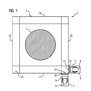
Figure 1 (FIG 1) shows a first exemplary embodiment of a
magnetooptical current sensor 1 for detecting an amperage of an
electrical current in a current conductor 2. The current
transducer 1 comprises a light coupling unit 3, a first exemplary
embodiment of an optical waveguide 5, and a light decoupling
unit 7.
The light coupling unit 3 has an input collimator 9 and a linear
input polarizer 11. The input collimator 9 is configured to
bundle light of a light source (not shown), for example of a
light-emitting diode. The input polarizer 11 polarizes light so
Date recue/Date received 2023-02-24
CA 03193133 2023-02-24
- 7 -
that linearly polarized light is supplied to the optical
waveguide 5.
The optical waveguide 5 is configured to supply light supplied
thereto from the light coupling unit 3 to the light decoupling
unit 7. The optical waveguide 5 displays the Faraday effect.
When a current flows in the current conductor 2, the polarization
direction of the light is rotated during the passage of the
optical waveguide 5 due to the Faraday effect.
The light decoupling unit 7 has an output polarizer 13 and a
linear output collimator 15. A fraction of the light output by
the optical waveguide 5 is transmitted by the output polarizer
13 which is parallel to a polarization axis of the output
polarizer 13. The output collimator 15 bundles the light
transmitted by the output polarizer 13 and supplies it to a
photodetector (not shown). The photodetector is configured to
detect the light intensity of the light supplied thereto. For
example, the photodetector is designed as a photodiode. The
amperage of the electrical current through the current conductor
2 is determined on the basis of the light intensity detected by
the photodetector.
The optical waveguide 5 of this exemplary embodiment is designed
as a glass ring which extends in a ring shape around the current
conductor 2. The current conductor 2 extends orthogonally to the
plane of the drawing of Figure 1. The optical waveguide 5 is
formed by four optical waveguide sections 17 to 20, which are
each formed as a prismatoid from glass. A first optical waveguide
section 17 extends from the light coupling unit 3 to a second
optical waveguide section 18. The second optical waveguide
section 18 extends between the first optical waveguide section
17 and a third optical waveguide section 19. The third optical
waveguide section 19 extends between the second optical
waveguide section 18 and the fourth optical waveguide section
20. The fourth optical waveguide section 20 extends from the
Date recue/Date received 2023-02-24
CA 03193133 2023-02-24
- 8 -
third optical waveguide section 19 to the light decoupling unit
7. A longitudinal axis of the first optical waveguide section
17 is orthogonal to longitudinal axes of the second optical
waveguide section 18 and the fourth optical waveguide section
20 and parallel to a longitudinal axis of the third optical
waveguide section 19.
An end face 21, facing toward the light coupling unit 3, of the
first optical waveguide section 17, which is orthogonal to the
plane of the drawing of Figure 1, has a first antireflective
coating 31. An end face 22 of the first optical waveguide section
17 opposite to this end face 21 is tilted in relation to the
plane of the drawing of Figure 1 by 450 (see also Figure 2 in
this regard). Light which runs through the first optical
waveguide section 17 along the longitudinal axis of the first
optical waveguide section 17 is totally reflected toward the
second optical waveguide section 18 at the end face 22. In the
second optical waveguide section 18, the light is incident on
an end face 23 (see Figure 2) of the second optical waveguide
section 18, which is also tilted by 450 in relation to the plane
of the drawing of Figure 1, and light is deflected by total
reflection in parallel to the longitudinal axis of the second
optical waveguide section 18. Accordingly, the light is guided
from the second optical waveguide section 18 to the third optical
waveguide section 19 and from the third optical waveguide
section 19 to the fourth optical waveguide section 20. An end
face 24, facing toward the light decoupling unit 7, of the fourth
optical waveguide section 20, which is orthogonal to the plane
of the drawing of Figure 1, has a second antireflective coating
32.
The first antireflective coating 31 increases the light
intensity of the light coupled into the optical waveguide 5 by
approximately 10 to 20% in relation to an embodiment of the
optical waveguide 5 without the first antireflective coating 31.
The second antireflective coating 32 increases the light
Date recue/Date received 2023-02-24
CA 03193133 2023-02-24
- 9 -
intensity of the light decoupled from the optical waveguide 5
by approximately 10 to 20% in relation to an embodiment of the
optical waveguide 5 without the second antireflective coating
32. Furthermore, the second antireflective coating 32 reduces
reflections of light at the end face 24 which reflect light back
into the optical waveguide 5.
Figure 2 (FIG 2) shows an optical waveguide 5 embodied similarly
to Figure 1 in an area in which the first optical waveguide
section 17 borders the second optical waveguide section 18. In
this example, the first optical waveguide section 17 and the
second optical waveguide section 18 are manufactured from
glasses different from one another, which have indices of
refraction different from one another. The first optical
waveguide section 17 and the second optical waveguide section
18 are adhesively bonded to one another by an adhesive layer 33,
which has an index of refraction which is between the indices
of refraction of the two optical waveguide sections 17, 18.
Reflections of light during the passage from the first optical
waveguide section 17 into the second optical waveguide section
18 are thus advantageously reduced in relation to an embodiment
of the optical waveguide 5 without the adhesive layer 33.
Figure 3 (FIG 3) shows a second exemplary embodiment of a
magnetooptical current sensor 1 for detecting an amperage of an
electrical current in a current conductor 2. This exemplary
embodiment has an optical waveguide 5, which is designed as a
fiber-optic optical waveguide and extends with a plurality of
turns in a ring shape around the current conductor 2. The ends
of the optical waveguide 5 each have a ferrule 41, 42. Each
ferrule 41, 42 has an end face 21, 24 having an antireflective
coating 31, 32.
Figure 4 (FIG 4) shows a detail of an optical waveguide 5 for a
magnetooptical current sensor 1, which has optical waveguide
sections 43, 44 having indices of refraction different from one
Date recue/Date received 2023-02-24
CA 03193133 2023-02-24
- 10 -
another. For example, the optical waveguide sections 43, 44 are
manufactured from different glasses from one another or are
formed by fiber-optic optical waveguides different from one
another. An antireflective layer 45 is arranged between two
adjoining optical waveguide sections 43, 44, which reduces
reflections of light during the passage of light between the
optical waveguide sections 43, 44 in relation to an embodiment
of the optical waveguide 5 without the antireflective layer 45.
Although the invention was illustrated and described in more
detail by preferred exemplary embodiments, the invention is not
thus restricted by the disclosed examples and other variations
can be derived therefrom by a person skilled in the art without
leaving the scope of protection of the invention.
Date recue/Date received 2023-02-24