Note: Descriptions are shown in the official language in which they were submitted.
WO 2022/066016
PCT/NL2021/050580
1
Optical assembly
The present invention relates to an optical assembly comprising a first
optical circuit and a
second optical circuit. The invention further relates to an optical device in
which the first optical
circuit and second optical circuit are fixedly connected to each other. In
addition, the present
invention relates to a method for manufacturing the optical device.
An optical assembly as defined in the preamble of claim 1 is known from WO
2016/131906. In this known optical assembly, the first optical circuit is an
optically active circuit
and comprises an optically active substrate, at least one first optical
waveguide formed in the
optically active substrate, and a first tapered recess in the optically active
substrate an-anged near a
first end of the at least one first optical waveguide, said first tapered
recess having a bottom
surface, an end surface, and a pair of side surfaces extending from the bottom
surface.
In the known optical assembly, the second optical circuit is an optically
passive circuit that
is formed by an interposer that includes at least one second optical
waveguide. The interposer
enables the at least one first waveguide on the optically active circuit to be
coupled to at least one
optical fiber. More in particular, on one end of the interposer, the at least
one second waveguide is
coupled to an optical fiber, whereas on another end the at least one second
waveguide is coupled to
the at least one first optical waveguide of the optically active circuit.
By fully removing the substrate underneath an end of the at least one second
optical
waveguide of the optically passive circuit, a finger is formed. This finger is
visible both from the
top and bottom of the interposer structure, which may aid in the alignment of
the finger into a first
tapered recess of the optically active circuit. In this manner, the end of the
at least one second
waveguide on the interposer becomes flexible allowing it to be arranged in the
first tapered
recesses. Generally, multiple fingers arc formed for connecting a plurality of
second optical
waveguides on the optically passive circuit to a corresponding plurality of
first optical waveguides
on the optically active circuit.
Permanent fiber-chip coupling via the interposer can be provided by affixing
the fingers
into positions permanently. This can be achieved using index matching
adhesives when the
adhesive is in the optical path between the interposer and the at least one
first waveguide of the
optically active circuit. Alternatively, adhesives such as solder can be used
outside of the first
tapered recess for fixedly connecting the interposer to the optically active
circuit.
Electrical connections between the interposer and the optically active circuit
can be
realized using one or more metal layers that cover the fingers and that make
contact with metal
pads on the optically active circuit.
In the known optical assembly, the alignment of the fingers is performed using
the fingers
themselves as a visual indicator. This was made possible by fully removing the
substrate
CA 03193678 2023- 3- 23
WO 2022/066016
PCT/NL2021/050580
2
underneath them. Moreover, the alignment requires the interposer to be
positioned at an angle
relative to the optically active circuit. This complicates the alignment,
reduces the reliability of the
coupling between the interposer and the optically active circuit, and only
allows one interposer to
be connected to the optically active circuit at a time.
It is an object of the present invention to provide an optical assembly in
which the
abovementioned problems associated with coupling of the first and second
optical circuit do not
occur or at least to a lesser extent.
This object is achieved using the optical assembly of claim 1 that is
characterized in that
the first optical circuit further comprises a second tapered recess arranged
near a second end of a
first optical waveguide among the at least one first optical waveguide, said
second tapered recess
having a bottom surface, an end surface, and a pair of side surfaces extending
from the bottom
surface, and in that the second optical circuit further comprises a first
recess arranged underneath a
first end of a second optical waveguide among the at least one second optical
waveguide, and a
second recess underneath a second end of a second optical waveguide among the
at least one
second optical waveguide.
Said first end of a second optical waveguide and said second end of a second
optical
waveguide form a first and second flexible end, respectively, wherein the
first and second flexible
end extend away from the second optical substrate along at least partially
opposite directions in
absence of external forces acting thereon.
According to the invention, said first and second flexible end are configured
to be received
in the first and second tapered recess, respectively, for the purpose of
allowing the first and second
flexible end to exert a spring force onto thc end surface of the first and
second tapered recess,
respectively, when fixedly coupling the first and second optical circuit. When
the first and second
optical circuit are fixedly connected, the first optical waveguide having the
first tapered recess
arranged near its first end is optically coupled via the end surface of the
first tapered recess to the
second optical waveguide having the first recess arranged near its first end
and the first optical
waveguide having the second tapered recess arranged near its second end is
optically coupled via
the end surface of the second tapered recess to the second optical waveguide
having the second
recess arranged near its second end.
Furthermore, the first optical circuit is one among an optically active
circuit and an
optically passive circuit and the second optical circuit is the other among
the optically active circuit
and an optically passive circuit.
Due to the spring force exerted onto the end surfaces, the first optical
circuit can at least be
partially clamped when connecting the first and second optical circuits.
Moreover, the spring force
ensures a low-loss optical coupling between the first flexible end and said
first end of a first optical
waveguide and between the second flexible end and said second end of a first
optical waveguide.
CA 03193678 2023- 3- 23
WO 2022/066016
PCT/NL2021/050580
3
The first optical circuit may be an optically active circuit, and the second
optical circuit
may be an optically passive circuit. Within the context of the present
invention, an optically active
circuit is an optical circuit that at least for the most part increases the
optical energy by converting
electrical energy supplied to the optically active circuit into optical
energy. Conversely, an
optically passive circuit is a circuit that at least for the most part only
dissipates optical energy.
Said first end of a first optical waveguide and said second end of a first
optical waveguide
can be ends at opposite sides of a same first optical waveguide.
Alternatively, said first end of a
first optical waveguide and said second end of a first optical waveguide can
be ends of different
first optical waveguides, said different first optical waveguides preferably
being arranged in
parallel.
The first optical circuit may further comprise one or more first contact pads,
and a first
alignment mark. In addition, the second optical circuit may further comprise
one or more second
contact pads and a second alignment mark. In this case, the one or more first
contact pads are
configured to be fixedly connected to the one or more second contact pads,
e.g. using an eutectic
bond, solder, or a conductive adhesive. Furthermore, the first optical circuit
and the second optical
circuit can be configured such that when the first optical circuit and the
second optical circuit have
been mutually moved to bring the first and second alignment mark into a
predefined lateral
registration, and the first optical circuit and second optical circuit are
subsequently brought closer
together without substantially changing the lateral registration, the first
and second flexible end are
guided towards said first end of a first optical waveguide and said second end
of a first optical
waveguide by the bottom surface and at least one of the side surfaces of the
first and second
tapered recess, respectively, thereby enabling an optical coupling between
said first flexible end
and said first end of a first optical waveguide and between said second
flexible end and said second
end of a first optical waveguide.
The first and second alignment marks allows for accurate lateral alignment.
For example,
the first optical substrate and the second optical substrate are both
essentially planar structures
extending in an x-direction and a y-direction. Prior to connecting the first
optical circuit and the
second optical circuit, the circuits are mutually moved in the x-direction
and/or y-direction until
the distance in these directions between the first and second alignment mark
meets a predetermined
value. For example, the alignment marks may be said to be aligned when the
distance in the y-
direction equals 500 +/- 5 micrometer and the distance in the x-direction
equals 300 +/- 5
micrometer. In a particular embodiment, the alignment marks are said to be
aligned when the
distance is less than 5 micrometers in both directions. Consequently, the
mutual alignment of the
first and second optical circuit can be relatively course, for example having
a tolerance that is
much greater than a characteristic dimension, e.g. width, of the at least one
first or second optical
waveguide. The final alignment between the flexible ends and the at least one
first optical
CA 03193678 2023- 3- 23
WO 2022/066016
PCT/NL2021/050580
4
waveguide, of which the accuracy must in general be better than the
abovementioned 5
micrometer, is facilitated due to the self-alignment of the flexible ends in
the tapered recesses.
During the alignment of the first and second alignment mark, the first and
second flexible
end do not engage any of the surfaces of the first and second tapered recess,
respectively.
However, once the alignment marks are aligned, the first optical circuit and
the second optical
circuit are mutually moved in the z-direction. During this movement, the first
and second flexible
end will engage the first and second tapered recess, respectively. More in
particular, the first and
second flexible end will engage the bottom surface and at least side surface
of the first and second
tapered recess. respectively. Due to the shape of the first and second tapered
recess, that tapers
outwardly moving away from said first or second end of a first optical
waveguide, respectively, the
first and second flexible end will be guided towards said first or second end
of a first optical
waveguide. Due to the upward bending of the first and second flexible end it
is ensured that the
first and second flexible end engage the first or second tapered recess,
respectively, even though
the first optical circuit and the second optical circuit are still spaced
apart in the z-direction.
Furthermore, the upward bending ensures that sufficient force is exerted onto
the first and second
flexible end by the end surfaces of the first and second tapered recess,
respectively, and vice versa,
to aid proper positioning of the first and second flexible end relative to the
first optical
waveguide(s) and to ensure a low-loss optical coupling. More in particular,
the end surfaces
provide for a controllable end position allowing the flexible ends to stop at
a same position.
Furthermore, this positioning need not be disturbed by the presence of any
adhesive on the second
optical waveguide(s) or in the first or second tapered recess, as the fixed
connection between the
first optical circuit and the second optically circuit is realized using the
one or more first contact
pads and the one or more second contact pads.
A distance between the first and second flexible end prior to the first and
second optical
circuits engaging each other can be greater than a distance between the end
surface of the first
tapered recess and the end surface of the second tapered recess, and a
distance between the first
and second flexible end, if these ends are bent to he in line with the
corresponding second optical
waveguide, is smaller than a distance between the end surface of the first
tapered recess and the
end surface of the second tapered recess. In this manner, it can be ensured
that the first and second
flexible ends have to deform, preferably elastically, thereby exerting the
spring force onto the end
surfaces of the first and second tapered recess, respectively.
The first and second flexible end may extend away from the second optical
substrate along
a first direction and second direction, respectively, each of the first and
second direction having a
component parallel to the second optical substrate and a component
perpendicular to the second
optical substrate, wherein the parallel components corresponding to the first
and second flexible
end point in at least partially opposite directions. By exerting a spring
force from at least partially
CA 03193678 2023- 3- 23
WO 2022/066016
PCT/NL2021/050580
opposite directions, an at least partial clamping can be obtained of the first
optical circuit by the
second optical circuit. Furthermore, each parallel component may be divided in
a second
component along a third direction and a third component along a fourth
direction perpendicular to
the third direction, wherein the second component corresponding to the first
direction is opposite to
5 the second component corresponding to the second direction and/or wherein
the third component
corresponding to the first direction is opposite to the third component
corresponding to the second
direction. In this manner, the spring forces can be applied symmetrically.
Here, a component is
said to be opposite to another component if it has the opposite sign and also
preferably an equal
magnitude.
The optical assembly may comprise a plurality of said first tapered recesses
for a
corresponding plurality of first optical waveguides, a plurality of said
second tapered recesses for a
corresponding plurality of first optical waveguides, a plurality of said first
flexible ends for a
corresponding plurality of second optical waveguides, and a plurality of said
second flexible ends
for a corresponding plurality of second optical waveguides, each first and
second flexible end
being configured to be received in a respective first and second tapered
recess, respectively, the
first and second flexible ends each extending away from the second optical
substrate along a
respective first direction and a respective second direction, respectively,
each of the respective first
and second direction having a component parallel to the second optical
substrate and a component
perpendicular to the second optical substrate. Each respective parallel
component can be divided in
a second component along a third direction and a third component along a
fourth direction
perpendicular to the third direction, and a sum of the second components
and/or a sum of the third
components can be substantially zero. Preferably, it can be achieved that the
combined spring force
exerted onto the first optical circuit can be substantially zero in at least
one of the third and fourth
direction.
The at least one second optical waveguide may comprise a first layer arranged
on a second
layer. Moreover, when the first and second optical circuits are fixedly
connected, the first layer is
arranged in between the second layer and the first optical substrate. The
first layer can he under
tensile strain relative to the second layer or the second layer can be under
compressive strain
relative to the first layer. Due to the imbalance in strain in the second
optical waveguide, when
etching away material underneath the first end of a second optical waveguide
for the purpose of
creating the first recess, the first end of the second optical waveguide will
bend upward thereby
creating the first flexible end. Flexibility of the first flexible end of the
second optical waveguide is
related to the width and thickness of the second optical waveguide. Similar
considerations apply
when creating the second flexible end.
CA 03193678 2023- 3- 23
WO 2022/066016
PCT/NL2021/050580
6
The first layer can only be provided on the second layer in a region
corresponding to the
first and second flexible end. In other regions of the at least one second
optical waveguide the first
layer may be omitted as the difference in strain is not required.
A maximum angle of inclination of the first and second flexible end relative
to a plane
parallel to the second optical substrate may lie in a range between 1 and 45
degrees, and more
preferably between 3 and 30 degrees. Outside of this range, the first and
second flexible end are at
risk of breaking or they will not extend sufficiently far into the first or
second tapered recess,
respectively, during the mutual movement in the z-direction of the first
optical circuit and the
second optical circuit. In addition, a length of the first and second flexible
end may lie in a range
between 50 and 1000 micrometer. Additionally or alternatively, a width of the
first and second
flexible end may lie in a range between 0.5 and 20 micrometer, and a thickness
of the first and
second flexible end may lie within a range between 50 and 150 percent of the
width of the first and
second flexible end, respectively.
A width of the at least one first optical waveguide may lie in a range between
0.1 and 10
micrometer, and a thickness of the at least one first optical waveguide may
lie in a range between
0.1 and 5 micrometer.
Various functions may be implemented in the optically active circuit and the
optically
passive circuit. For example, at least one passive element of the group of
passive elements
consisting of a filter, a combiner, a polarization convertor, and a splitter,
may be implemented in
the optically passive circuit. Additionally or alternatively, at least one
active element of the group
of active elements consisting of a laser, a semiconductor optical amplifier, a
phase modulator, an
amplitude modulator, and a photodetector may be implemented in the optically
active circuit. In
this latter case, the optically active circuit may comprise one or more
electrical terminals connected
to the at least one active clement for receiving or outputting an electrical
signal and/or for receiving
electrical power, wherein at least one among the one or more electrical
terminals is connected to
and/or formed by a respective first contact pad among the one or more first
contact pads.
Accordingly, the same structure can he used for fixedly connecting the
optically active circuit and
the optically passive circuit as for realizing the required electrical
connection for operating the at
least one active element.
The first optical waveguide among the at least one first optical waveguide may
end in the
corresponding first and/or second tapered recess. For example, the
corresponding first and/or
second tapered recess may comprise a first segment in which said first optical
waveguide among
the at least one first optical waveguide ends. This first segment may be wider
than a last part of that
first optical waveguide but smaller than the first or second flexible end of
the corresponding
second optical waveguide that is to be received in said corresponding first or
second tapered recess.
The corresponding first and/or second tapered recess may comprise a second
segment connected to
CA 03193678 2023- 3- 23
WO 2022/066016
PCT/NL2021/050580
7
the first segment. The second segment may be wider than both the first segment
and the first or
second flexible end of the corresponding second optical waveguide that is to
be received in said
corresponding first or second tapered recess. Furthermore, a boundary between
the first and second
segments can be configured to form the end surface of the corresponding first
or second tapered
recess against which the first or second flexible end of the corresponding
second optical waveguide
that is to be received in said corresponding first or second tapered recess
abuts after having fixedly
connected the one or more first and second contact pads.
Alternatively, an end facet of the first optical waveguide that is arranged
near the
corresponding first or second tapered recess may form the end surface of that
tapered recess.
The optically active circuit may further comprise a first contact ring
arranged around the at
least one first optical waveguide, and the optically passive circuit may
further comprise a second
contact ring arranged around the at least one second optical waveguide,
wherein the first and
second contact rings are configured to be fixedly connected to each other for
the purpose of
providing a sealing for the at least one first optical waveguide and the at
least one second optical
waveguide. Such sealing may be beneficial for protecting the coupling between
the at least one
first optical waveguide and the at least one second optical waveguide against
environmental
conditions, such as humidity and pollutants, and/or protecting the exposed
facets of the flexible
ends and/or protecting the exposed facets of the at least one first optical
waveguide.
The one or more first contact pads and the one or more second contact pads may
each
comprise one or more metal layers to allow them to be connected through
soldering, preferably
eutectic soldering, or bonding, preferably eutectic bonding, using the
simultaneous application of
heat and pressure. Prior to connecting the first and second contact pads,
solder or another adhesive
may be applied to at least one of the first and second contact pads. Similar
considerations hold for
the first and second contact rings.
The first or second optical substrate corresponding to the optically active
circuit may
comprise a first cladding layer having a first doping type, a second cladding
layer having a second
doping type different from the first doping type, and an active layer arranged
in between the first
and second cladding layers. The at least one first or second optical waveguide
being part of the
optically active circuit may have been formed by etching through at least a
part of the first cladding
layer. Additionally or alternatively, the optically active circuit may
comprise a first metal contact
to the first cladding layer that is connected to a respective first or second
contact pad among the
one or more first or second contact pads, and a second metal contact to the
second cladding layer
that is connected to a respective first or second contact pad among the one or
more first or second
contact pads.
The first cladding layer may comprise a first sublayer, a second sublayer, and
a first etch
stop layer arranged in between the first and second sublayers. The first etch
stop layer can be a stop
CA 03193678 2023- 3- 23
WO 2022/066016
PCT/NL2021/050580
8
layer for stopping a particular wet-chemical etching step. The at least one
first or second optical
waveguide being part of the optically active circuit may have been formed by
etching up to the first
etch stop layer. Similarly, the second cladding layer may comprise a first
sublayer, a second
sublayer, and a second etch stop layer arranged in between the first and two
sublayers, wherein the
second metal contact has been formed by an etch up to the second etch stop
layer and a metal layer
arranged in the cavity formed by said etch. The second etch stop layer can be
a stop layer for
stopping a particular wet-chemical etching step.
The first and second cladding layers can be made from indium phosphide,
gallium
arsenide, or gallium antimonide, and/or wherein the second cladding layer is
arranged on an
indium phosphide, gallium arsenide, or gallium antinnonide substrate having a
same doping type as
the second cladding layer. The active layer can be made from indium gallium
arsenide phosphide,
aluminum indium gallium arsenide or antimonide based materials. However, the
present invention
is not limited to these materials.
The optically passive substrate may comprise a guiding layer, a carrier
substrate, and a
cladding layer arranged in between the guiding layer and the carrier
substrate. In this case, the at
least one first or second optical waveguide being part of the optically
passive circuit has been
formed by etching through the cladding layer and guiding layer, preferably up
to the carrier
substrate. Additionally or alternatively, when the second optical circuit is
the optically passive
circuit, the first and second flexible end of said a second optical waveguide
among the at least one
second optical waveguide have been formed by partially etching the carrier
substrate underneath
the cladding layer. Furthermore, a stress layer may be arranged on the guiding
layer, which stress
layer is under tensile strain and which stress layer is configured to cause,
at least in part, the
upward bending of the first and second flexible waveguide. The stress layer
can be a silicon nitride
layer Six1\1, but the invention is not limited thereto.
The guiding layer can be a silicon layer, preferably a monocrystalline layer.
Furthermore,
the cladding layer can be a silicon oxide layer Si3Oy, and the carrier
substrate may comprise a
silicon substrate.
Alternatively, the guiding layer can be embedded into the cladding layer,
wherein the
guiding layer is a silicon nitride layer SiõNy, and the cladding layer is a
silicon oxide layer SiõOy. In
this case, the at least one first or second optical waveguide being part of
the optically passive
circuit can be formed by etching through the cladding layer, preferably up to
the carrier substrate.
The optical assembly may further comprise a further optically active circuit
configured as
the aforementioned optically active circuit. In such case, the optically
passive circuit can be
configured to be coupled to the further optically active circuit in a same
manner as to the
aforementioned optically active circuit.
CA 03193678 2023- 3- 23
WO 2022/066016
PCT/NL2021/050580
9
According to a second aspect, the present invention relates to an optical
device comprising
the optical assembly as described above, wherein the optically active circuit,
and in so far as
present, the further optically active circuit, is/are fixedly connected to the
optically passive circuit.
According to a third aspect, the present invention relates to a method for
manufacturing the
abovementioned optical device in so far as the first optical circuit comprises
one or more first
contact pads and a first alignment mark, and the second optical circuit
further comprises one or
more second contact pads and a second alignment mark. This method comprises
mutually moving
the first optical circuit and the second optical circuit to bring the first
and second alignment mark
into a predefined lateral registration. The method further comprises the step
of, after having
obtained the predefined lateral registration, bringing the first and second
optical circuit closer
together without substantially changing the lateral registration during which
movement the first
and second flexible end are guided towards said first end of a first optical
waveguide and said
second end of a first optical waveguide by the bottom surface and at least one
of the side surfaces
of the first and second tapered recess, respectively, thereby enabling an
optical coupling between
said first flexible end and said first end of a first optical waveguide and
between said second
flexible end and said second end of a first optical waveguide. As a final
step, the first and second
optical circuit are fixedly connected by fixedly connecting the one or more
first contact pads to the
one or more second contact pads.
Next, the present invention will be described in more detail referring to the
appended
drawings, wherein:
Figures 1A and 1B illustrate a schematic cross section of coupling an
optically active
circuit to an optically passive circuit in accordance with the present
invention;
Figures 2A and 2B illustrate top views of coupling an optically active circuit
coupled to an
optically passive circuit in accordance with the present invention and figures
2C and 2D illustrate a
perspective view of tapered recess and the arrangement of a flexible end in
such recess,
respectively;
Figures 3A and 3B illustrate an optical device and a wafer holding a plurality
of said
devices, respectively;
Figures 4A-4D illustrate different processing steps for manufacturing an
optically active
circuit in accordance with the present invention;
Figures 5A-5D illustrate different processing steps for manufacturing an
optically passive
circuit based on silicon-on-insulator technology;
Figures 6A-6D illustrate different processing steps for manufacturing an
optically passive
circuit wherein the optical waveguides are formed using a silicon nitride
layer embedded in a
silicon oxide layer; and
CA 03193678 2023- 3- 23
WO 2022/066016
PCT/NL2021/050580
Figure 7A illustrates a decomposition of the direction along which a flexible
end extends
away from the second optical substrate, and figure 7B illustrates an example
in which the forces
exerted by the flexible ends in different directions substantially compensate
each other.
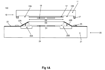
In figure 1A, an assembly 100 is shown that comprises an optically active
circuit 10 and an
5 optically passive circuit 20 in an uncoupled state. Optically active
circuit 10 is shown
schematically as having an optically active substrate 11 comprising an
optically active layer 12.
Here, a first optical waveguide is formed using optically active layer 12. At
the opposite ends of
this waveguide, a tapered recess 13A, 13B is provided. Furthermore, first
contact pads 14 are
provided, which are typically realized using one or more metal layers. As
shown, a distance
10 between the end walls of tapered recesses 13A, 13B equals a distance D2.
Optically passive circuit 20 comprises an optically passive substrate 21 in
which second
optical waveguides 22 are formed. Recesses 23 are arranged near ends of
waveguides 22. Due to
the partial removal of substrate 21 underneath these ends, flexible ends 22A,
22B are formed that
bend upwards under an angle 0 relative to a plane that is parallel to
substrate 21. In addition,
second contact pads 24 are provided that are typically made using one or more
metal layers. In
addition, as shown, a distance between the tips of ends 22A, 22B equals a
distance D3.
Furthermore, a distance between the tips of ends 22A, 22B when these ends 22A,
22B lie parallel
to substrate 21 equals a distance Dl. As shown, D3>D2>D1.
Figure 1B shows assembly 100 in a coupled state. As shown, ends 22A have been
guided
towards the end walls of tapered recesses 13A, 13B so that the optical signal
can be efficiently
transferred from optical layer 12 to waveguide 22. Flexible ends 22A, 22B bend
upwards under an
angle 0' relative to a plane that is parallel to substrate 21, wherein 0' < 0.
In the uncoupled state, if
flexible ends 22A, 22B were bent upwards under the angle 0', a distance
between the tips of ends
22A, 22B would be less than D2. In this manner, it is ensured that flexible
ends 22A, 22B would
deform, preferably elastically, when coupling optically active circuit 10 and
optically passive
circuit 20 thereby exerting a force onto the end surfaces or walls of tapered
recesses 13A, 13B.
Furthermore, first contact pads 14 are fixedly connected to second contact
pads 24, e.g. by
means of an intermediate solder layer or by a eutectic bonding. These contact
pads can be used to
transfer electrical signals and/or electrical power via the optically passive
circuit 20 towards
optically active circuit 10.
Figures 2A and 2B illustrate the process of coupling optically active circuit
10 to optically
passive circuit 20 in top view. Figures 2C and 2D illustrate a perspective
view of tapered recesses
13A, 13B and the arrangement of flexible ends 22A, 22B in recesses 13A, 13B,
respectively.
As shown, a first alignment mark 15 is arranged on optically active substrate
11. Similarly,
a second alignment mark 25 is arranged on optically passive substrate 21. In
order to couple
circuits 10, 20, optically active circuit 10 is positioned relative to
optically passive circuit 20 using
CA 03193678 2023- 3- 23
WO 2022/066016
PCT/NL2021/050580
11
alignment marks 15, 25. For example, optically active circuit 10 is moved
while optically passive
circuit 20 is kept stationary to bring alignment marks 15, 20 in a predefined
lateral registration. A
predefined lateral registration is achieved when a distance between marks 15,
20 in both the x-
direction and y-direction falls within a predefined range, e.g. between 45 and
48 micron. In a
particular embodiment, the range for both x-direction and the y-direction is
centered around 0.
By comparing figure 2A, which shows the uncoupled state, with figure 2B, which
shows
the coupled state, it can be observed that ends 22A 22B have been brought into
close proximity of
waveguides 12. This has been achieved by ends 22A, 2213 being pushed by a
bottom surface of
recesses 13A, 13B and at least one side surface thereof towards a position at
which ends 22A, 22B
exert a spring force onto the end surfaces of tapered recesses 13A, 13B. This
is shown in more
detail in figure 2C.
Figure 2C shows a perspective view of an embodiment of a tapered recess 13A.
Here,
recess 13A comprises a first part formed by bottom surface 131 and side
surfaces 132. A facet 12A
of waveguide 12 exits in this first part. Recess 13A further comprises a
second part formed by
bottom surface 131, side surfaces 133, 134 and rear surface 135.
Figure 2D shows a top view of recess 13A in which a flexible end 22A has been
arranged.
Here, it can be seen that side surfaces 133, which form a boundary between the
first and second
parts of recess 13A, run substantially parallel to end facet 12A. Furthermore,
a width of the first
part, as measured in the x-direction, is greater than a width of waveguide 12
but less than a width
of flexible end 22A. On the other hand, a width of the second part, also
measured in the x-
direction, is greater than a width of flexible end 22A. Only at the corner
between surfaces 133,
134, the width of the second part may be substantially identical to the width
of flexible end 22A.
As shown in figure 2D, side surfaces 133 form end surfaces against which
flexible ends 22A press.
Furthermore, as can be seen from figure 2D, the light from waveguide 12 will
pass through air
before entering flexible end 22A.
Figure 3A illustrates a hybrid photonic integrated circuit, 'PIC, 200 wherein
a plurality of
optically active circuits 10 is coupled to a single optically passive circuit
20. Here, each of the
optically active circuits 10 performs a function such as light generation,
amplification, switching,
modulation, or detection, on each of two optical waveguides arranged on the
optically active
substrate. On optically passive circuit 20, waveguides 22 guide the various
optical signals to a filter
30. It would be clear to the skilled person that PIC 200 is but a mere example
of how various active
functions can be realized on optically active circuit 10 and how various
passive functions can be
realized on optically passive circuit 20. The invention is therefore not
limited to the example
shown. Furthermore, the active functions typically require electric power
and/or require and/or
produce electrical signals. These can be transferred between optically passive
circuit 20 and
optically active circuit 10 using contact pads 14, 24.
CA 03193678 2023- 3- 23
WO 2022/066016
PCT/NL2021/050580
12
Figure 3B illustrates a wafer 26 of which the optically passive substrates 21
are part. As
shown, optically active circuits 10 can be mounted on optically passive
circuits 20 while the
substrates thereof are still mutually connected. After final processing, PICs
200 can be separated
using known dicing techniques such as sawing.
Figures 4A-4D illustrate a process for manufacturing an optically active
circuit 10 in
accordance with the invention. Here, it is noted that for figures 4A-4D, the
upper figure illustrates
a cross sectional view whereas the bottom figure illustrates a schematic top
view. In each bottom
figure, a line is indicated that indicates where the cross sectional view is
taken.
The process shown in figures 4A-4D is based on indium phosphide technology and
uses a
semiconductor wafer comprising a layer stack as indicated in figure 4A. This
layer stack comprises
an indium phosphide (InP) substrate 10 with several epitaxial layers 1-9, as
indicated in table 1.
Table 1
Layer no in Fig. 3A Description layer Layer no in Fig. 3A
Description layer
1 InGaAs 7 InP n-
doped
3 InP p-doped 8 etch stop
layer
4 etch stop layer 9 InP n-
doped
5 InP p-doped 10 InP
substrate
6 Active layer
Figure 4B illustrates a first step in which contact layer 1 is partially
removed and in which
a waveguide has been formed by etching down to etch stop layer 4. More in
particular, an etching
technique is used for etching through the major part of layer 3. This etching
step can be well
controlled as it stops when it reaches layer 4.
A similar approach is followed for defining a contact to the n-doped InP
layers. This is
shown in figure 4C. This same etching step, up to etch stop layer 8, is used
for defining tapered
recess 303.
As shown in figure 4D, an anti-reflection, 'AR', coating layer 304 is applied,
which is
subsequently opened at the positions where an Ohmic contact should be
realized. A patterned
metal layer 308 is used for realizing a contact to InGaAs layer 1, hereinafter
referred to as the P-
contact, and another patterned metal layer 307 to n-doped InP layer 9,
hereinafter refen-ed to as the
N-contact. As a final step, interconnect metal is applied for the N-contact
and P-contact. This may
be performed using a sputtering process.
Figures 5A-5D illustrate different processing steps for manufacturing an
optically passive
circuit based on silicon-on-insulator technology. This processing uses a layer
stack as illustrated in
figure 5A. Here, a high resistivity silicon substrate 52 is preferably used
that is covered by a buried
CA 03193678 2023- 3- 23
WO 2022/066016
PCT/NL2021/050580
13
silicon oxide 51. A layer 50 of monocrystalline silicon is arranged on top of
the buried silicon
oxide. Furthermore, it is noted that for figures 5A-5D, the upper figure
illustrates a cross sectional
view whereas the bottom figure illustrates a schematic top view. In each
bottom figure, a line is
indicated that indicates where the cross sectional view is taken.
As a first step, shown in figure 5B, a silicon nitride Si,N, layer 400 is
deposited to
introduce sufficient tensile strain to cause the ends of the waveguides to be
formed to bend
upwards. This layer is removed from other parts of the circuit.
As a second step, also shown in figure 5B, a shallow etch is performed on
silicon layer 50
to define a ridge waveguide therein. More in particular, a shallow recess 53
is defined. As a next
step, also shown in figure 5B, a relatively deep recess 54 is etched inside
recess 53 down to the
buried silicon oxide layer 51. Thereafter, as shown in figure 5C, an
antiretlective coating layer 401
is applied. Metallization 402 will be applied for routing power and/or
electrical signals to and from
the optically active circuit that is to be connected to the optically passive
circuit. Next, a relatively
thick electroplated metal 403 is applied for achieving low ohmic resistance
and for allowing
eutectic bonding. Following, in figure 5D, an opening 55A is defined followed
by a dry etching
step to etch through the antireflection coating layer 401 and the buried oxide
layer 51. As a final
step, an anisotropic etch is performed to remove silicon substrate 52
underneath an end of the
waveguide. The anisotropic etch will generate a cavity 55. Due to the residual
strain in this
waveguide, formed in figure 5D using layers 400, 50, 51, the end will bend
upwards and away
from silicon substrate 52, similar to what is shown in figures 1A and 1B. By
ensuring that the
width w of end of the waveguide is comparable to its height h, torsion in the
end of the waveguide
caused by engagement with the tapered recess during the process of aligning
the end of the
waveguide to the waveguides on the optically active circuit as shown in
figures 1-2 can be
prevented.
Figures 6A-6D illustrate different processing steps for manufacturing an
optically passive
circuit wherein the optical waveguides are formed using a silicon nitride
layer embedded in a
silicon oxide layer. it is noted that for figures 6A-6D, the upper figure
illustrates a cross sectional
view whereas the bottom figure illustrates a schematic top view. In each
bottom figure, a line is
indicated that indicates where the cross sectional view is taken.
As shown in figure 6A, a silicon substrate 71 is used on top of which a
silicon oxide SixOy
layer 70A is thermally grown which will act as a cladding layer. Thereafter, a
silicon nitride Si,Ny
layer 72 is deposited that will act as a guiding layer. After defining the
waveguide using etching, a
further silicon oxide SixOy layer 70B is grown. In this manner, guiding layer
72 is completely
embedded in cladding layer 70A, 70B.
As a next step, shown in figure 6B, a Si,N, layer 73, which introduces tensile
strain, is
deposited only at those positions where the upward bending ends of the
waveguides need to be
CA 03193678 2023- 3- 23
WO 2022/066016
PCT/NL2021/050580
14
defined. Furthermore, the optical waveguide is defined by etching through
cladding layers 70A,
70B up to silicon substrate 71.
As a next step, shown in figure 6C, an AR layer 74 and metals 75, 76 are
applied. As
shown in figure 6D, an opening 77A is created in AR layer 74 for subsequent
anisotropic etching
of substrate 71 as shown in figure 6E. After etching away substrate 71, a
cavity 77 is formed and
the end of the waveguide will bend upwards.
Figure 7A illustrates a decomposition of the direction along which a flexible
end extends
away from the second optical substrate, and figure 7B illustrates an example
in which the forces
exerted by the flexible ends in different directions substantially compensate
each other.
In figure 7A, a flexible end 80 is shown that extends relative to the x-y
plane, which plane
is parallel to optically passive substrate 21. The direction along which
flexible end 80 extends can
be decomposed in a component c2 that is parallel to the x-y plane and in a
component cl that is
perpendicular to the x-y plane. In turn, parallel component c2 can be
decomposed in a second
component c2_1 along the x-axis and a third component c2_2 along the y-axis.
The decomposition shown in figure 7A can be performed for each flexible end.
For
example, figure 7B illustrates an optically active circuit 86 that is mounted
on an optically passive
circuit 85. Optically passive circuit 85 comprises four flexible ends 80
corresponding to four
waveguides 81. In addition, optically passive circuit 86 comprises four
tapered recesses 84 by
which flexible ends 80 are optically coupled to waveguides 82 on optically
active circuit 86.
Optically active circuit 86 further comprises an active component 83 that
generates or acts on
optical signals in waveguides 82.
Each of the flexible ends 80 extends away from the optically passive substrate
along a
different direction. By applying the decomposition scheme of figure 7A, it can
be verified that the
parallel components corresponding to these different directions, when added
together, would
substantially cancel each other. In this manner, it can be ensured that
optically active circuit 86 is
clamped by optically passive circuit 85 in a substantial symmetric manner.
In the above, the present invention had been explained using detailed
embodiments thereof.
It should be apparent that the invention is not limited to these embodiments
but that various
modifications are possible without deviating from the scope of the invention,
which is defined by
the appended claims.
CA 03193678 2023- 3- 23