Note: Descriptions are shown in the official language in which they were submitted.
WO 2022/067011
PCT/US2021/051914
REDUCED ELECTRONIC SAMPLING OF APTAMER SENSORS
CROSS-REFERENCE TO RELATED APPLICATIONS
[0001]
This application claims the benefit of the filing dates of U.S. Patent
Application
Serial No. 63/083,023, filed on September 24, 2020, U.S. Patent Application
Serial No.
63/150,675, filed on February 18, 2021, U.S. Patent Application Serial No.
63/197,669, filed
on June 7, 2021, and U.S. Patent Application Serial No. 63/215,605, filed on
June 28. 2021,
the disclosures of which are incorporated by reference herein in their
entireties.
BACKGROUND OF THE INVENTION
1100021
This section is intended to introduce the reader to various aspects of the
art that may
be related to various aspects of the invention, which are described and/or
claimed below. This
discussion is believed to be helpful in providing the reader with background
information to
facilitate a better understanding of various aspects of the invention.
Accordingly, it should be
understood that these statements are to be read in this light, and not as
admissions of prior art.
[0003]
Aptamers are molecules that bind to a specific target molecule.
Electrochemical
aptamer sensors include an aptamer that specifically binds to an analyte of
interest, and that is
attached to an electrode. The aptamer has an attached redox active molecule
(redox couple)
which can transfer electrical charge to or from the electrode. When an analyte
binds to the
aptamer, the aptamer changes shape, changing the availability of a redox
couple to transfer
charge with the electrode. This results in a measurable change in electrical
current that can be
translated into a measure of the concentration of the analyte.
1100041
A major unresolved challenge for aptamers is extending the lifetime of the
sensors,
especially for applications where continuous operation is required, such as
multiple
measurements over time by the same device. Redox couples do not have infinite
lifetime.
Typically, the more they are used the more they degrade. The same is also true
of the other
materials/layers in the device, such as the blocking layer which reduces
baseline current, the
aptamer attachment to the electrode, the electrode material itself, and other
materials/chemicals
used in the sensor.
1100051
Thus, a need exists for improved device design and methods to reduce the
electrochemical-induced degradations of aptamer sensor devices over time. Such
an
innovation could broadly advance the ability of aptamer sensors to be used in
continuous or
1
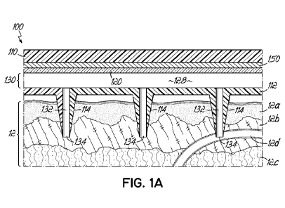
CA 03193809 2023- 3- 24
WO 2022/067011
PCT/US2021/051914
long duration sensing applications such as wearable or implantable sensors,
and other types of
applications.
SUMMARY OF THE INVENTION
[0006]
Certain exemplary aspects of the invention are set forth below. It should
be
understood that these aspects are presented merely to provide the reader with
a brief summary
of certain forms the invention might take, and that these aspects are not
intended to limit the
scope of the invention.
[0007]
Many of the drawbacks and limitations stated above can be resolved by
creating
novel and advanced interplays of chemicals, materials, sensors, electronics,
microfluidics,
algorithms, computing software, systems, and other features or designs, in a
manner that
affordably, effectively, conveniently, intelligently, or reliably brings
sensing technology into
proximity with sample fluids containing at least one analyte of interest to be
measured.
[0008]
In an embodiment of the invention, a sensing device for measuring an
analyte is
provided. The sensing device includes a sensor and a detection circuit. The
sensor includes a
working electrode with an aptamer and an attached redox couple to
electrochemically measure
the analyte. The detection circuit is operatively coupled to the sensor, and
is configured to
perform a partial scan of the sensor that only includes a portion of a full
scan.
[0009]
In an aspect of the invention, the working electrode may be one of a
plurality of
working electrodes configured to measure the analyte, and the detection
circuit may be
configured to perform the partial scan on a different subset of the plurality
of working
electrodes on each of at least two consecutive measurement cycles.
[0010]
In another aspect of the invention, a plurality of subsets of the working
electrodes
may be scanned, and each subset may include at least three electrodes that are
all scanned as
part of a single measurement cycle.
[0011]
In another aspect of the invention, the plurality of working electrodes
may include
at least 2, 3, 5, 10, 50, 100, 200, 500, or 1000 electrodes.
[0012]
In another aspect of the invention, the partial scan may be one of a
partial voltage
scan, a partial current scan, or a partial frequency scan.
[0013]
In another aspect of the invention, the partial scan may include providing
a signal
having a plurality of sampling periods to the sensor. Each sampling period may
include a
sampling duration, at least one set of consecutive sampling periods may be
separated by a
ramping period having a ramping duration, and the ramping duration may be at
least 0.2%,
1.0%, 2.0%, 5.3%, 11.1%, 25.0%, 100%, 900%, or 1900% of the sampling duration.
2
CA 03193809 2023- 3- 24
WO 2022/067011
PCT/US2021/051914
[0014]
In another aspect of the invention, the detection circuit may be further
configured
to partially scan the sensor a plurality of times at time intervals that are
periodic, non-periodic,
or random.
[0015]
In another aspect of the invention, the partial scan may be one of a
plurality of
partial scans each associated with a measurement cycle, and the portion of the
full scan
provided by each partial scan may vary between measurement cycles.
1100161
In another aspect of the invention, the detection circuit may be further
configured
vary the portion of the full scan provided by each partial scan between
measurement cycles.
[0017]
In another aspect of the invention, each of the plurality of partial scans
may have at
least one of a starting voltage and an ending voltage, and the detection
circuit may be further
configured to shift at least one of the starting voltage and the ending
voltage between
measurement cycles.
[0018]
In another aspect of the invention, the partial scan may include a first
portion that
generates a baseline sample range, and a second portion that generates a peak
sample range.
[0019]
In another aspect of the invention, the baseline sample range may only
cover a
portion of a baseline region, and the peak sample range may only cover a
portion of a peak
region generated by the full scan.
[0020]
In another aspect of the invention, one or more of the peak region and the
baseline
region may be defined based on a slope of an output generated by the partial
scan.
1100211
In another aspect of the invention, the full scan may have a voltage range
of at least
0.4 volts, and the partial scan may have a voltage range of no more than 0.2
volts or 0.1 volts.
[0022]
In another aspect of the invention, the first portion of the full scan
range may be
scanned less frequently than the second portion of the full scan range.
1100231
In another aspect of the invention, the second portion of the full scan
range is
scanned at least two times, five times, 10 times, 50 times, or 100 times as
frequently as the first
portion of the full scan range.
[0024]
In another aspect of the invention, the partial scan may have a duty cycle
that is less
than 75%, 50%, 20%, 10%, 5%, 2%, or 1% of the full scan.
[0025]
In another aspect of the invention, the partial scan may generate less
than 0.75 times,
0.50 times, 0.20 times, 0.10 times, 0.05 times, 0.02 times, 0.01 times, or
0.001 times the total
charge transfer generated by the full scan.
[0026]
In another aspect of the invention, the partial scan may be a partial
current scan
having a current range that is <90%, <50%, <20%, <10%, <5% or <2% of the
current range of
a full current scan.
3
CA 03193809 2023- 3- 24
WO 2022/067011
PCT/US2021/051914
[0027]
In another aspect of the invention, the partial scan may be a partial
frequency scan
having a frequency range that is <50%, <20%, <10%, <5%, or <2% of the
frequency range of
a full frequency scan.
[0028]
In another embodiment of the invention, a method of measuring an analyte
is
provided. The method includes partially scanning the sensor that includes the
working
electrode having the aptamer and the attached redox couple to
electrochemically measure the
analyte, and partially scanning the sensor includes only providing a portion
of the full scan to
the sensor.
[0029]
In an aspect of the invention, the working electrode may be one of the
plurality of
working electrodes configured to measure the analyte, and the method may
further include
performing the partial scan on the different subset of the plurality of
working electrodes on
each of the at least two consecutive measurement cycles.
[0030]
In another aspect of the invention, the plurality of subsets of the
working electrodes
may be scanned, each subset may include at least three electrodes, and the
method may further
include scanning all of the at least three electrodes as part of a single
measurement cycle.
1100311
In another aspect of the invention, partially scanning the sensor may
include
performing a partial voltage scan, a partial current scan, or a partial
frequency scan.
[0032]
In another aspect of the invention, partially scanning the sensor may
include
providing the signal having the plurality of sampling periods to the sensor.
Each sampling
period may have a sampling duration, at least one set of consecutive sampling
periods of the
plurality of sampling periods may be separated by the ramping period having
the ramping
duration, and the ramping duration may be at least 0.2%, 1.0%, 2.0%, 5.3%,
11.1%, 25.0%,
100%, 900%, or 1900% of the sampling duration.
1100331
In another aspect of the invention, the method may further include
partially
scanning the sensor a plurality of times, wherein the partial scans occur at
time intervals that
are periodic, non-periodic, or random.
[0034]
In another aspect of the invention, each of the plurality of partial scans
may be
associated with a measurement cycle, and the portion of the full scan provided
by each partial
scan may vary between measurement cycles.
[0035]
In another aspect of the invention, the partial scan may be a partial
voltage scan
including one or more portions of a voltage range associated with the full
scan.
[0036]
In another aspect of the invention, the partial voltage scan may include
one or more
voltage scans that cover a cumulative voltage range of less than 0.2 volts.
4
CA 03193809 2023- 3- 24
WO 2022/067011
PCT/US2021/051914
[0037] In another aspect of the invention, the method may further
include partially
scanning the sensor a plurality of times, wherein each of the plurality of
partial scans is
associated with a measurement cycle, and each partial scan has at least one of
a starting voltage
and an ending voltage that is shifted in voltage over time between measurement
cycles.
[0038] In another aspect of the invention, the one or more
portions of the voltage range
may include at least one baseline partial scan of the baseline region, and at
least one peak partial
scan associated with the full scan.
[0039] In another aspect of the invention, the method may further
include partially
scanning the sensor a plurality of times to generate a plurality of partial
scans. A first portion
of the plurality of partial scans may include at least one baseline partial
scan, a second portion
of the plurality of partial scans may include at least one peak partial scan,
and the number of
partial scans in the second portion of the plurality of partial scans may be
greater than the
number of partial scans in the first portion of the plurality of partial
scans.
[0040] In another aspect of the invention, an electrical charge
may be transferred by the
partial scan that generates less than half of the electrical charge transfer
associated with the full
scan.
[0041] In another aspect of the invention, partially scanning the
sensor may include
performing a partial current scan, and the partial current scan may have a
duration that is less
than 90% of the amount of time a full current scan would take to transfer 98%
of the total
charge transferred by the full scan.
[0042] In another aspect of the invention, partially scanning the
sensor may include
performing a partial frequency scan, and the partial frequency scan may
include less than
50% of a full scanning frequency range.
[0043[ In another aspect of the invention, the partial frequency
scan may include at least
one peak frequency for changes in signal gain.
[0044] In another aspect of the invention, the partial frequency
scan may include at least
one peak frequency with no signal gain.
[0045] In another aspect of the invention, partially scanning the
sensor may include
scanning the first portion of the full scan that generates the baseline sample
range, and
scanning the second portion of the full scan that generates the peak sample
range.
[0046] hi another embodiment of the invention, another sensing
device for measuring the
analyte is provided. The sensing device includes the sensor and the detection
device
operatively coupled to the sensor. The sensor includes a plurality of working
electrodes each
having an aptamer and an attached redox couple to electrochemically measure
the analyte.
CA 03193809 2023- 3- 24
WO 2022/067011
PCT/US2021/051914
The detection circuit is configured to perform a scan of the sensor by
scanning a different
subset of the plurality of working electrodes on each of at least two
consecutive measurement
cycles.
[0047] In another embodiment of the invention, another method of
measuring an analyte
is provided. The method includes scanning a first subset of the working
electrodes during a
first measurement cycle, and scanning a second subset of the working
electrodes during a
second measurement cycle that follows the first measurement cycle, wherein the
first subset
is different from the second subset.
BRIEF DESCRIPTION OF THE DRAWINGS
[0048] The objects and advantages of the disclosed invention will
be further appreciated in
light of the following detailed descriptions and drawings in which:
[0049] FIGS. 1A and 1B are cross-sectional views of an exemplary
sensing device in
accordance with an embodiment of the invention.
[0050] FIG. IC is a schematic view of an exemplary sensing device
in accordance with
another embodiment of the invention.
[0051] FIGS. 2A-2C are graphical views illustrating sampling
methods to reduce the
electrochemical sampling imparted on an electrochemical aptamer based sensor
that uses
voltage scans.
[0052] FIG. 2D is a graphical view illustrating exemplary ways of
defining peak and
baseline regions of a voltage scan.
[0053] FIGS. 3A and 3B are graphical views illustrating sampling
methods to reduce the
electrochemical sampling imparted on an electrochemical aptamer based sensor
that uses
current scans.
[0054] FIGS. 4A and 4B are graphical views illustrating sampling
methods to reduce the
electrochemical sampling imparted on an electrochemical aptamer based sensor
that uses
frequency scans.
1100551 FIGS. 5A and 5B are graphical views illustrating scanning
signals that may be
provided to a sensor of the sensing devices of FIGS. 1A-1C.
DEFINITIONS
[0056] As used herein, the term "about," when referring to a
value or to an amount of mass,
weight, time, volume, pH, size, concentration, or percentage, is meant to
encompass variations
of, in some embodiments 20%, in some embodiments 10%, in some embodiments
5%, in
6
CA 03193809 2023- 3- 24
WO 2022/067011
PCT/US2021/051914
some embodiments 1%, in some embodiments 0.5%, and in some embodiments 0.1%
from
the specified amount, as such variations are appropriate to perform the
disclosed methods and
operate the disclosed devices.
[0057]
As used herein, the term "aptamer" means a molecule that undergoes a
conformation change as an analyte binds to the molecule, and which satisfies
the general
operating principles of the sensing methods and devices as described herein.
Such molecules
are, e.g., natural or modified DNA, RNA, or XNA oligonucleotide sequences,
spiegelmers,
peptide aptamers, and affimers. Modifications may include substituting
unnatural nucleic acid
bases for natural bases within the aptamer sequence, replacing natural
sequences with unnatural
sequences, or other suitable modifications that improve sensor function.
Typically, aptamers
used in electrochemical sensors are tagged with a redox molecule such as
methylene blue.
[0058]
The devices and methods described herein encompass the use of sensors. A
sensor,
as used herein, is a device that is capable of measuring the concentration of
a target analyte in
solution. As used herein, an -analyte" may be any inorganic or organic
molecule, for example:
a small molecule drug, a metabolite, a hormone, a peptide, a protein, a
carbohydrate, a nucleic
acid, or any other composition of matter. The target analyte may comprise a
drug. The drug
may be of any type, for example, including drugs for the treatment of cardiac
system, the
treatment of the central nervous system, that modulate the immune system, that
modulate the
endocrine system, an antibiotic agent, a chemotherapeutic drug, or an illicit
drug. The target
analyte may comprise a naturally-occurring factor, for example a hormone,
metabolite, growth
factor, neurotransmitter, etc. The target analyte may comprise any other
species of interest, for
example, species such as pathogens (including pathogen induced or derived
factors), nutrients,
and pollutants, etc.
[0059]
As used herein, the term "duty cycle" refers to the portion of a scanning
signal (e.g.,
a voltage signal that is varied within a voltage range, a current signal that
is varied within a
current range, or a frequency that is varied within a frequency range) that is
applied during
operation of a sensor as a percentage of the "full scan", which is the total
available voltage,
current, and/or frequency range typically used for operation of the sensor.
[0060]
As used herein, the term "continuous sensing" may be satisfied by the
device
recording a plurality of readings over a period of time during which the
sensing occurs. Thus,
even a point-of-care testing device which provides a single data point can be
considered a
continuous sensing device if, for example, the test has a 15 minute duration,
and the testing
device operates by taking multiple data points over 15 minutes and averaging
them to provide
a single data measure.
7
CA 03193809 2023- 3- 24
WO 2022/067011
PCT/US2021/051914
DETAILED DESCRIPTION OF THE INVENTION
[0061]
One or more specific embodiments of the invention will be described below.
In an
effort to provide a concise description of these embodiments, all features of
an actual
implementation may not be described in the specification. It should be
appreciated that in the
development of any such actual implementation, as in any engineering or design
project,
numerous implementation-specific decisions must be made to achieve the
developers' specific
goals, such as compliance with system-related and business-related
constraints, which may
vary from one implementation to another. Moreover, it should be appreciated
that such a
development effort might be complex and time consuming, but would nevertheless
be a routine
undertaking of design, fabrication, and manufacture for those of ordinary
skill having the
benefit of this disclosure.
[0062]
Certain embodiments of the disclosed invention show sensors as simple
individual
elements. It is understood that many sensors require two or more electrodes,
reference
electrodes, or additional supporting technology or features that, for purposes
of clarity, are not
necessarily described herein. Sensors measure a characteristic of an analyte.
Sensors are
preferably electrical in nature, but may also include optical, chemical,
mechanical, or other
known sensing mechanisms. Sensors can be in duplicate, triplicate, or more, to
provide
improved data and readings. Sensors may provide continuous or discrete data
and/or readings.
Certain embodiments of the disclosed invention may show certain sub-components
of sensing
devices, but may omit additional sub-components needed for use of the device
in various
applications that are known, e.g., a battery, antenna, adhesive. These
omissions may be for
purposes of brevity and to focus on certain inventive aspects of the disclosed
embodiments of
the invention. All ranges of parameters disclosed herein include the endpoints
of the ranges.
[0063]
With reference to FIG. 1A, and in accordance with an embodiment of the
invention,
an exemplary sensing device 100 is shown placed partially in-vivo into skin 12
including an
epidermis 12a, a dermis 12b, and a subcutaneous or hypodermis 12c. The sensing
device 100
includes a non-conductive substrate 110 (e.g., a polymer), a microneedle
assembly 112, a
sensing layer 120, and an electrode layer 150 that couples the sensing layer
120 to the substrate
110. A portion of the sensing device 100 receives a fluid, e.g., an invasive
biofluid such as an
interstitial fluid from the dermis 12b and/or blood from a capillary 12d.
Access to the fluid
may be provided, for example, by the microneedle assembly 112. The microneedle
assembly
112 may be formed of metal, polymer, semiconductor, glass, or other suitable
material, and
include a plurality of microneedles 114. Each microneedle 114 may include a
lumen 132
having an inlet 134 that provides access to the fluid.
8
CA 03193809 2023- 3- 24
WO 2022/067011
PCT/US2021/051914
[0064]
The sensing device 100 may further include a sample volume 128 comprising
a
space 130 defined between the microneedle assembly 112 and the sensing layer
120, and the
lumens 132. The sensing layer 120 and electrode layer 150 may form a working
electrode of
the sensing device 100. The sample volume 128 may be filled with a
microfluidic component
such as capillary channels, a hydrogel, or other suitable material, that
operatively couples the
fluid to the sensing layer 120. Thus, a diffusion and/or advective flow
pathway may be
provided between the fluid to be sensed and the sensing layer 120. This
pathway may begin at
the inlets 134 to the microneedles 114 and reach the sensing layer 120.
Alternative
arrangements and materials may also be possible, such as using a single
needle, hydrogel
polymer microneedles, or other suitable means to couple the fluid to one or
more sensors. Thus,
embodiments of the invention are not limited to the depicted sensing device
100. In addition,
a portion of sensing device 100, or even the entire sensing device 100, could
be implanted into
the body and perform similarly as described herein. For example, the electrode
layer 150 and
sensing layer 120 may be implanted inside the body on the end of an indwelling
needle like
those used in continuous glucose monitors.
1100651
With further reference to FIG. 1A, the sensing layer 120 may be affinity-
based, and
may include, for example, one or more aptamers. The aptamers may be selective
in reversible
binding to an analyte, thiol bonded to the electrode layer 150, and used to
sense an analyte by
means of electrochemical detection. The electrode layer 150 may include a
suitable conductive
material, such as gold, carbon, or other suitable electrically conducting
material. The sensing
device 100 may be electrical in nature, and may utilize an attached redox
couple to transduce
the electrochemical signal. The sensing device 100 may also measure changes in
impedance
between the working electrode and the fluid being sensed.
[0066[
Although the exemplary embodiments depicted by FIGS. 1A and 1B use
microneedles to access an interstitial fluid, it should be understood that
embodiments of the
invention are not so limited. Thus, it should be further understood that the
principles of the
invention may apply to additional applications of aptamer sensors, such as
sensors for
monitoring environmental pollutants, for food processing safety, for implanted
sensors, or for
any other suitable applications and devices.
[0067]
With reference to FIG. 1B, where like numerals refer to like features in
the previous
figures, the sensing device 100 may include a plurality of working electrodes
152 for sensing
one or more analytes. By way of example, the plurality of working electrodes
152 may include
one or more working electrodes 152a having an electrode layer 150a and a
sensing layer 120a
configured to detect a drug such as cocaine, and another one or more working
electrodes 152b
9
CA 03193809 2023- 3- 24
WO 2022/067011
PCT/US2021/051914
having an electrode layer 150b and a sensing layer 120b configured to detect a
metabolite, such
as phenyalanine. In an alternative embodiment, both sets of one or more
working electrodes
152a, 152b may be configured to detect a single analyte, such as doxorubicin.
Thus, the sensing
device 100 may include one or more sensors for each of one or more analytes.
[0068]
FIG. 1C depicts an exemplary sensing device 156 that includes a sensor 158
and a
detection circuit 160. The sensor 158 includes one or more electrodes, e.g., a
working electrode
162, a reference electrode 164, and a counter electrode 166. The detection
circuit 160 may
include a voltage sensor 168, a current sensor 170, a voltage source 172, and
a controller 174.
The voltage sensor 168 may be operatively coupled to the working and reference
electrodes
162, 164 to measure a voltage therebetween. The current sensor 170 may be
operatively
coupled to the working and counter electrodes 162, 166 to measure a current
flowing
therebetween. The voltage source 172 may be operatively coupled to the working
and counter
electrodes 162, 166, and may be controlled by the controller 174 to
selectively apply voltages
between the working and counter electrodes 162, 166.
[0069]
The controller 174 may comprise a computing device that includes a
processor 176,
a memory 178, an input/output (I/0) interface 180, and a Human Machine
Interface (HMI)
182. The processor 176 may include one or more devices selected from
microprocessors,
micro-controllers, digital signal processors, microcomputers, central
processing units, field
programmable gate arrays, programmable logic devices, state machines, logic
circuits, analog
circuits, digital circuits, or any other devices that manipulate signals
(analog or digital) based
on operational instructions stored in memory 178. Memory 178 may include a
single memory
device or a plurality of memory devices including, but not limited to, read-
only memory
(ROM), random access memory (RAM), volatile memory, non-volatile memory,
static random
access memory (SRAM), dynamic random access memory (DRAM), flash memory, cache
memory, or data storage devices such as a hard drive, optical drive, tape
drive, volatile or non-
volatile solid state device, or any other device capable of storing data.
[0070]
The processor 176 may operate under the control of an operating system 184
that
resides in memory 178. The operating system 184 may manage computer resources
so that
computer program code embodied as one or more computer software applications
186 residing
in memory 178 can have instructions executed by the processor 176. One or more
data
structures 188 may also reside in memory 178, and may be used by the processor
176, operating
system 184, or application 186 to store or manipulate data.
1100711
The I/0 interface 180 may provide a machine interface that operatively
couples the
processor 176 to other devices and systems, such as the voltage sensor 168,
current sensor 170,
CA 03193809 2023- 3- 24
WO 2022/067011
PCT/US2021/051914
and voltage source 172. The application 186 may thereby work cooperatively
with the other
devices and systems by communicating via the I/O interface 180 to provide the
various
features, functions, applications, processes, or modules comprising
embodiments of the
invention.
[0072]
The HMI 182 may be operatively coupled to the processor 176 of controller
174 to
allow a user to interact directly with the sensing device 156. The HMI 182 may
include video
or alphanumeric displays, a touch screen, a speaker, and any other suitable
audio and visual
indicators capable of providing data to the user. The HMI 182 may also include
input devices
and controls such as an alphanumeric keyboard, a pointing device, keypads,
pushbuttons,
control knobs, microphones, etc., capable of accepting commands or input from
the user and
transmitting the entered input to the processor 176.
[0073]
Referring again to FIG. 1B, the sensing device 100 may use a plurality of
working
electrodes 152 each configured to detect the same analyte, but the sensors may
not always be
used simultaneously. That is, different working electrodes or subsets
including one or more of
a plurality of working electrodes may be selectively used at different times
to detect the same
analyte, thereby extending the working lifetime of the working electrodes 152.
To prolong the
use of the sensing device 100, an embodiment of the invention may use a
sensing device
comprising a plurality of working electrodes. In operation, a subset of the
plurality of working
electrodes may be used for multiple sequential scans until one or more
electrodes in the subset
of electrodes fails. In response to detecting this failure, the sensing device
may switch to
another functional electrode for subsequent scans. When that electrode fails,
the process may
be repeated. Each subset of electrodes may consist of an individual electrode,
or any number
of electrodes that is less than the total number of electrodes in the
plurality of electrodes.
Subsets of the plurality of electrodes may be overlapping or non-overlapping.
Overlapping
subsets include one or more electrodes that are also members of one or more
other subsets with
which they overlap, while non-overlapping subsets do not include any
electrodes that are
members of more than one of the non-overlapping subsets.
[0074]
In an alternative embodiment, each sequential scan may be conducted on a
different
electrode or subset of electrodes until they have all been used, at which
point the process
repeats. Sequential scanning may be advantageous because electrodes can
degrade and change
over time due to other factors. Thus, sequential scanning may allow for a more
easily
interpretable continuum of data to be recorded over time as compared to use-to-
failure
embodiments. In any case, sequential scans may be performed in a periodic, a
non-periodic,
11
CA 03193809 2023- 3- 24
WO 2022/067011
PCT/US2021/051914
or random manner. For example, measurement cycles may occur at predetermined
intervals of
time, at intervals of time having a predetermined pattern, or at random
intervals of time.
[00751
In an exemplary embodiment, an electrochemical aptamer-based (EAB) sensing
device may use the same type of reference and counter electrodes for all the
aptamer sensor
electrodes. By way of example, at least 2, 3, 5, 10, 50, 100, 200, 500, or
1000 sensor electrodes
may be used in one EAB sensing device, although embodiments of the invention
are not limited
to any particular number of sensor electrodes. For example, if 200 electrodes
are used, each
individual electrode may experience 0.005 the electrochemical fatigue during a
particular use
period as compared to a single electrode having to support all the
measurements during that
use period. This method may effectively reduce the duty cycle that any one
electrode must
experience while sustaining the frequency of measurements needed to support
continuous
sensing. For example, a drug measurement that must be taken every minute for
three days
would require 4320 measurements in total over the measurement period. A single
sensor would
have to support 4320 measurements, whereas 10 sensors as taught herein would
each
individually only have to support around 432 such measurements. In some cases,
measuring
multiple electrodes simultaneously or near in time to each other can reduce
measurement error,
e.g., by measuring multiple sensors for each datapoint.
[0076]
Embodiments of the invention may permit a subset of sensors (e.g., a
subset of
electrodes or sensors) to be measured at any given time to reduce measurement
error or to
improve the statistical validity of a measurement. The subset of sensors
measured may change
over time to increase the measurement lifetime of the sensing device unit. As
a non-limiting
example, one sensor at a time can measure a drug while the concentration of
the drug is within
its safe therapeutic window. However, during dosing of the drug and rapid
uptake in the body,
the drug concentration may be higher initially. To achieve more accurate data,
three or more
sensors could be used to represent each datapoint. Alternatively, one sensor
could be used
more often (e.g., every 5 minutes right after drug ingestion vs. every 30
minutes or every 3
hours after drug ingestion). As a result, the amount of sampling of the sensor
may be reduced,
thereby improving its longevity.
[0077]
FIG. 2A depicts a graph 200 in accordance with another exemplary
embodiment of
the invention. The graph 200 includes a plot 290 of current verses voltage for
a full scan (e.g.,
VMIN to VmAx) of an exemplary sensor. In a typical operational environment,
Vm/N may be about
0 volts, and VIVIAN may be about 0.4 volts. Aptamers with redox tags on
working electrodes are
typically measured using a form of pulse voltammetry, such as Square Wave
Voltammetry
(SWV), although other methods may also be used. In SWV, a voltage (V) that
causes a
12
CA 03193809 2023- 3- 24
WO 2022/067011
PCT/US2021/051914
corresponding current output (I) is swept (as shown and described in more
detail below in
reference to FIG. 5A). The current results due to the redox couple
transferring electrical charge
to/from the working electrode. Whether S WV or another method is used to scan
the sensor, a
voltage scan range is typically used that provides a "full scan". A full scan
normally includes
a baseline region 290a, 290c having a baseline current, and at least one redox
peak region 290b.
Measuring the baseline current generated in the baseline region 290a, 290c may
improve
accuracy as the magnitude of the current in the peak region 290b can shift
over time as the
baseline current in the baseline region 290a, 290c increases or decreases.
This shift in
magnitude may be due to fouling, loss of the blocking layer, or other factors.
Furthermore, the
peak region 290b can also shift in voltage position over time due to effects
such as changes in
pH, fouling, analyte binding, salinity, reference electrode degradation, and
other factors.
Therefore, the voltage position of the peak region 290b may benefit from
tracking the peak
position over time.
[0078]
With reference to FIG. 2B, a partial scan may be substituted for a full
scan to reduce
electrochemical degradation of the electrochemical aptamer sensor. The size of
the voltage
scan range can be influenced by a number of SWV parameters including, but not
limited to,
the current range to be measured, the step frequency, and step width (which is
generally in
volts). However, during traditional measurements, most of the voltage scan
range probed may
not be necessary to determine EAB sensor response. Because electrical currents
and fields
experienced by the working electrode can degrade one or more materials that
form the aptamer
sensor, full scans may cause sensor degradation with each and every
measurement cycle as
compared to partial scans. Thus, eliminating irrelevant or lower value
measurement regions
can reduce active sensor time, and increase sensor longevity.
1100791
In a research environment, all regions of the voltage scan range may be
irrelevant
because a full scan is needed to confirm the data has a proper redox peak, and
because research
environments do not need sensors that last for days to run experiments. In
commercial
applications, it is possible to monitor only the voltage sub-regions that need
to be measured to
continuously confirm a high quality signal. Thus, in commercial settings,
partial scans may
allow longer duration operation, thereby cutting costs by replacing sensors
less frequently,
which is also desired commercially. This increased duration may be
particularly beneficial, as
once nuclease degradation of the aptamers is removed by membrane protection
and/or mutating
the aptamer sequence, and severe sensor surface fouling is prevented, the
electrochemical
degradation during sampling can be the dominant degradation mechanism.
13
CA 03193809 2023- 3- 24
WO 2022/067011
PCT/US2021/051914
[0080]
FIG. 2B depicts a partial scan that includes portions of the voltage scan
range which
produce a plurality of current baseline sample ranges 292a, 292c (e.g., two
current sample
ranges associated with scanning voltage sub-ranges V] - V, and Vs-V6.
respectively) and a current
peak sample range 292b (V3-V4). As shown in FIG. 2C, measurements may also be
made using
only two of these portions of the full scan, e.g., one current baseline sample
range 292a and the
current peak sample range 292b. A partial scan may include only one current
sample range, or
any number of current sample ranges so long as the scan voltage sub-ranges
used to generate
the current sample ranges do not collectively comprise the full voltage scan
range. FIG. 2A
may represent a forward voltammogram scan, a backward voltammogram scan, a net
voltammogram scan (e.g., forward and backward data are combined as illustrated
later in
FIG. 5A), a portion of a cyclic voltammogram, or some other scan, with the
main illustrative
point of FIG. 2A being that there exists a redox peak region and a baseline
region, and that
both provide information needed to evaluate signals from an aptamer based
sensor.
[0081]
With further reference to FIGS. 2B and 2C, a variety of methods may be
used to
reduce the effective duty cycle of voltage and current scans used to obtain a
sensor
measurement. For example, a baseline partial scan that produces current sample
ranges 292a
or 292c could be performed less often than a peak partial scan that produces
current sample
range 292b. Less frequent baseline partial scans may be acceptable because the
baseline signal
changes slowly and/or the baseline changes can be predictable. In contrast,
the peak signal can
change more rapidly and is typically less predictable because it reflects
changes in the
concentration of the analyte. For example, 292b could be measured every five
minutes whereas
292a could be measured only every 30 minutes. For example, a measurement of
the current
peak sample range 292b could be performed at least two times, five times, 10
times, 50 times,
or 100 times more often than a measurement of the current baseline sample
ranges 292a or
292c. Such an approach could be particularly beneficial if the redox peak
region 290b or 292b
lies at a position which also has little or minimal degradation of the
electrode, which may
depend on the electrode material (Au, carbon, etc.).
[0082]
Current baseline sample range 292a and/or current baseline sample range
292c may
also be measured in multiple ways. For example, by using an additional
electrode with no
redox couples, by varying the frequency of interrogation of the measurement
such that the
current peak sample range 292b is comparable to the current baseline sample
range that would
exist at that voltage where the peak 292b exists. This variable frequency
technique may take
advantage of the fact EAB sensors typically have a zero signal gain frequency.
These examples
show that the terms baseline and peak should not be narrowly limited to their
exact
14
CA 03193809 2023- 3- 24
WO 2022/067011
PCT/US2021/051914
representation shown in FIGS. 2A-2C, and should be more broadly interpreted so
long as they
achieve the desired outcome for embodiments of the invention, which is reduced
sampling of
an aptamer sensor.
[0083]
The maximum voltage VmAx applied to the sensor may also be reduced to
provide a
partial voltage scan and improved lifetime. For example, the voltage could be
scanned from
VMIN or VI to V4 in order to limit the maximum voltage applied to the device
and avoid voltages
that include 1/ to V6 and beyond. Therefore, the controller 174 may cause the
voltage source
172 to only scan up to the point where the peak current 292 is properly
measured (e.g., up to
V4) and not beyond. For example, a conventional scan will typically cover ¨0.4
volts or more,
and with embodiments of the invention, the scan length could be less than 0.2
volts or less than
0.1 volts to capture adequate baseline and peak. Even if the baseline is
partially affected by
the peak, the baseline can also be predicted from the partial shape of the
peak since the peak is
super-imposed on the baseline.
[0084]
Generally, a full voltage scan would include sufficient scanning before
and after the
redox peak voltage to capture baseline current values on both sides of the
peak. Thus, a full
voltage scan may be defined as a scan covering a voltage range that includes
the redox peak
and a sufficient amount of adjacent baseline where the additional current
contribution from
redox of the redox tag is less than 3% of the current contributed by redox of
the redox tag at
the peak redox tag current across the voltage range. Exemplary voltage scans
that may be
considered as partial scans include voltage scans having a voltage duty cycle
that is less than
75%, 50%, 20%, 10%, 5%, 2%, or 1% of the full voltage scan as defined above.
[0085]
A non-limiting example of a full voltage scan in one direction (negative
or positive)
or a net voltarnmogram for methylene blue is approximately 0 to -0.5 volts. In
this example,
the redox peak may occur from approximately -0.2 to -0.3 volts at near neutral
pH and with an
Ag/AgC1 reference electrode. As another example, consider ferricyanide with a
peak near -0.1
to -0.2 volts, or consider Nile blue with a wider redox peak spanning -0.3 to -
0.5 volts.
[0086]
Another way to distinguish partial voltage scans from full voltage scans
may be by
the total charge used to measure the sensor. For example, if a full voltage
scan generates a
total charge transfer of X coulombs, a voltage scan that generates less than
0.75 times, 0.50
times, 0.20 times, 0.10 times, 0.05 times, 0.02 times, 0.01 times, or even
0.001 times the total
charge transfer X may be considered as a partial voltage scan. Alternately,
the total charge
transfer of the redox peak could be X, which may be provided by integrating
the area under the
redox peak curve. In this case, a voltage scan that generates less than 0.75
times, 0.50 times,
CA 03193809 2023- 3- 24
WO 2022/067011
PCT/US2021/051914
0.20 times, 0.10 times, 0.05 times, 0.02 times, 0.01 times, or even 0.001
times the total charge
transfer X associated with the redox peak could he considered as a partial
voltage scan.
[00871
Measurement variables such as electrochemical aptamer sensor composition,
reference electrode characteristics (e.g., surface area), and environmental
factors such as pH
can change the position of key factors, such as current versus voltage values.
Therefore, a
methodology for determining key features and prediction their positions may be
used to
properly query sensors while minimizing oversampling that takes into account
these variables.
To this end, embodiments of the invention may monitor the position of baseline
and peak
currents overtime, and adjust the partial scanning voltages such that they
stay optimally aligned
with these positions. For example, periodically or as needed, a full voltage
scan could be
performed to reveal the positions of all peaks and baselines. For example, a
rising slope, apex
of the peak with zero slope or alternately positive slope followed by negative
slope, or falling
slope of the peak could be measured to monitor peak position. Slope values may
vary in a
predictable way based on measurement variables. Thus, the slope values used to
define
boundaries between peak regions and baseline regions of a scan may be set
based on the
particular measurement environment being used.
[0088]
By way of example, FIG. 2D depicts a graph 210 including an exemplary plot
212
of a voltage scan having a peak region 214, and a plot 216 showing the slope
(dildv) of the
voltage scan. The slope of the voltage scan may have a peak positive slope
SMAX_p at voltage
Vg, and a peak negative slope SMAX-N at voltage V9. A peak sample range 218
may be defined,
for example, as a portion of the peak region 214 between the peak positive
slope SmAx_p and the
peak negative slope SmAx_N. In an alternative embodiment, the peak sample
range 218 may be
defined as a percentage of the voltage range V8-V9 defined by the peak
positive and negative
slopes SMAX-P, SMAX-N, e.g., as 75%, 50%, 20%, 10%, 5%, 2%, or 1% of the
voltage range Vs-V9.
In another alternative embodiment, the peak sample range 218 may be defined as
a portion of
the voltage scan between a voltage V7 at which the scan slope exceeds a
positive slope threshold
STH p, and a voltage Vio at which the scan slope exceeds a negative slope
threshold STH N. Each
of the positive and negative slope thresholds SHTp, SHTN may be defined, for
example, as a
percentage of the peak positive slope SmAx_p and/or peak negative slope
SmAx_N, e.g., 75%, 50%,
20%, 10%, 5%, 2%, or 1% of the peak positive or peak negative slopes STII-P,
STII-N- The edges
of the peak region 214 may also be defined based on the slope of the voltage
scan passing
through one or more slope thresholds, and the peak position may be defined as
the scan voltage
at which the slope of the voltage scan passes through zero between the peak
positive and peak
negative slopes SmAx_p, SmAx_N. In an alternative embodiment, the edges of the
peak region 214
16
CA 03193809 2023- 3- 24
WO 2022/067011
PCT/US2021/051914
may be defined as being a predetermined voltage below the positive slope
threshold STH-p and
at a predetermined voltage above the negative slope threshold STH_N. In yet
another
embodiment, the peak edges and location may be defined by voltages at which
the current i of
the voltage scan exceeds one or more thresholds.
[0089]
The voltage scans may also shift predictably. To accommodate these shifts,
an
embodiment of the invention may automatically adjust the positions of the
voltage scans over
time without measurement at all, or only with intermittent measurements. For
example, if the
peak shifted by +2.4 mV every 60 minutes, the peak could be measured every
hour to confirm
the rate of peak shifting, and if the sensor was measured every 10 minutes,
the peak voltage
that is scanned would be automatically shifted by +0.4 mV for each 10 minutes.
[0090]
Scanning signals applied to the sensor of a sensing device may include
voltage scans
(as described above), current scans, frequency scans, and combinations of
voltage, current, and
frequency scans. FIG. 3A depicts a graph 300 including a plot 390 of a partial
current scan.
The partial current scan represented by plot 390 may be configured to reduce
electrochemical
degradation of the electrochemical aptamer sensor. The scan in FIG. 3A may be
a current scan
for an aptamer sensor in which the lifetime of the redox current decay is
independent of the
current amplitude. That is, the redox current decay is insensitive to
variations in the number
of aptamer probes on the electrode. This characteristic may allow such sensors
to be more
calibration free and less susceptible to drift. After double layer charging
effects (typically less
than 1 ms), the rest of the decay curve changes by several fold (more than an
order of
magnitude) due to a depletion of the number of redox reporters which still
have not transferred
an electron to/from the electrode. Such scanning is similar to
chronocoulometric measurement,
which measures total charge, not current.
[0091]
Thus, embodiments of the invention may also be applied to
chronocoulometric
measurements. As defined herein, a full current scan may start at t = 0 and
end at baseline
when greater than a threshold percentage (e.g., 98%) of the total charge
transfer from the redox
couples has occurred, or when greater than the threshold percentage of the
charged to be
transferred has been transferred, respectively.
The threshold percentage for
chronoamperometry is illustrated in FIG. 3A as reaching current baseline
sample range 390a.
FIG. 3A is a single example only as the time to reach current baseline sample
range 390a can
be <10 ms to >100 ms depending on redox reporter and its distance from and
kinetics related
to the electrode. As shown in FIG. 3B, a partial current scan current sample
range 390b is
utilized to reduce total current and therefore degradation of the sensor. It
can take a long time
for a sensor to reach baseline in chronoamperometry or chronocoulometry, which
imparts
17
CA 03193809 2023- 3- 24
WO 2022/067011
PCT/US2021/051914
additional degradation of a sensor electrode without much added benefit in
terms of the quality
of the sensor measurement. Therefore, the partial current scan can be <90%,
<50%, <20%,
<10%, <5% or <2% of the full current scan.
[0092]
FIG. 4A depicts a graph 400 including plots 490, 495 of current verse
frequency.
A partial frequency scan may be performed to reduce sampling of the sensor and
therefore
reduce sensor degradation. Aptamer sensors are normally optimized by scanning
both voltage
and frequency. For many aptamers, there are two or more frequencies that
provide maximal
signal change, one frequency being without the target analyte as shown by plot
490, and one
being with the target analyte, as shown by plot 495. The intersection of plots
490, 495 identify
a zero-signal gain region. Furthermore, an aptamer sensor may be optimized for
a frequency
that provides maximum signal gain for only a single "signal on" or "signal
off' configuration,
or both frequencies can be used to help preserve calibration or performance of
the sensor
measurement.
[0093]
By way of explaining this frequency effect more deeply, the application of
a voltage
bias to the sensor interface generates electrokinetic, faradaic, mass, and
charge transport
phenomena that affect the output of these sensors. First, the sample
electrolyte responds to
voltage perturbations by dynamically aligning to their electrical fields. This
effect generates
double-layer charging/discharging currents in electrochemical measurements.
Moreover, the
voltage perturbation may cause field-induced movement actuation of the
negatively charged
aptamer backbone. This effect perturbs the frequency of electron transfer
which, in turn, affects
sensor signaling currents. Beyond field-induced modulation of the electrolyte
and aptamer
strands, mass transport of the redox reporter to the electrode also affects
electron transfer.
Furthermore, aptamer secondary structures and the thickness of the electrode-
blocking
monolayer and any foulants on that surface affect the currents measured, as do
the standard
electron transfer rate of the redox reporter and the rates of receptor-target
ligand
association/dissociation. All of these factors can influence the ideal
measurement frequency
of aptamer sensors.
[0094]
Because the frequencies that provide maximal signal change can change
during
sensor use, a subset of frequencies may be scanned periodically to identify
any frequency
dependent changes. FIG. 4B depicts the graph 400 in FIG. 4B with current
sample ranges
490a, 495a that include at least one peak frequency for signal gain, and
current sample ranges
490b, 495b that include at least one frequency at which there is no signal
gain. The full
frequency range fully to fmAx may range from 1 Hz to 10 kHz and more
preferably from 10 Hz
to 1 kHz, and is represented by a horizonal axis having a log scale in graph
400. Partial
18
CA 03193809 2023- 3- 24
WO 2022/067011
PCT/US2021/051914
frequency scan ranges (e.g., fl-f2, f3-f5, f4-f6, f7-f8) corresponding to one
or more of these full
frequency scan ranges for the current sample ranges 490a, 495a, 490b, 495b may
be <50%,
<20%, <10%, <5%, or <2% of the total plotted frequency scan range on a log
scale vs.
frequency scale from 5 Hz to 5000 Hz. For example, a sensor could be sampled
with a partial
frequency scan during a measurement of a sensor, the partial frequency scan
comprising less
than 20% of the total plotted scanning range on a log scale vs. frequency
between 5 Hz and
5000 Hz.
[0095]
With reference to FIGS. 2A-2C, in some aptamer sensors there is a zero-
signal gain
frequency. Therefore, a sensor could be sampled only at a voltage that
minimizes electrode
degradation, such as the voltage position of methylene blue's peak on a gold
electrode. For
such a sensor, the signal gain may be simply measured at that peak voltage at
both a peak signal
gain frequency (e.g., associated with current sample ranges 490a, 495a) vs. a
zero signal gain
frequency (e.g., the intersection of current sample ranges 490b, 495b), in
order to further
minimize electrical degradation of the sensor.
[0096]
With reference to FIG. 1C, FIG. 5A depicts a graph 500 including a plot
502 of
voltage verses time of an electric signal that may be applied between the
working electrode
162 and the counter electrode 166 of sensing device 156, and a graph 504
including several
plots of current verses voltage, or voltammograms, of a measurement cycle. The
current used
to generate the plots of graph 504 may be the current flowing between the
working electrode
162 and the counter electrode 166, e.g., as measured by current sensor 170.
'the voltage used
to generate the plots of graph 504 may be the voltage between the working
electrode 162 and
the reference electrode 164, e.g., as measured by voltage sensor 168. The
electric signal
represented by plot 502 is an example of a SWV signal.
1100971
FIG. 5B depicts a graph 514 illustrating a method that reduces the amount
of
electronic sampling used during device measurement in accordance with an
embodiment of the
invention. In a square wave voltammetric experiment, the current at a working
electrode is
measured while the voltage between the working electrode and another electrode
(e.g., the
counter electrode) is pulsed forward and backward. The voltage waveform can be
viewed as a
superposition of a regular square wave onto an underlying staircase, as shown
by plot 502. In
this sense, SWV can be considered a modification of staircase voltammetry.
[0098]
The current may be sampled at two points during each cycle, e.g., once at
the end
of the forward voltage pulse (ifd) and again at the end of the reverse voltage
pulse (ib,d). Thus,
each sample is taken immediately before the voltage direction is reversed. As
a result of this
current sampling technique, the contribution to the current signal resulting
from capacitive
19
CA 03193809 2023- 3- 24
WO 2022/067011
PCT/US2021/051914
(sometimes referred to as non-faradaic or charging) current is minimal. As a
result of having
current sampling at two different instances per square-wave cycle, two current
waveforms are
collected. Both have diagnostic value, and are therefore preserved. When
viewed in isolation,
the forward and reverse current waveforms mimic the appearance of a cyclic
voltammogram
(which corresponds to the anodic or cathodic halves, however, is dependent
upon experimental
conditions). Despite both the forward and reverse current waveforms having
diagnostic worth,
it is almost always the case in SWV for the potentiostat software to plot a
differential current
waveform derived by subtracting the reverse current waveform from the forward
current
waveform. This differential curve is then plotted against the applied voltage.
Peaks in the
differential current vs. applied voltage plot are indicative of redox
processes, and the
magnitudes of the peaks in this plot are used to interpret measurement of the
concentration of
the analyte in the sample fluid.
[0099]
With respect to FIG. 5B, a reduced the amount of electronic sampling may
be
achieved in one or more ways. For example, a lower voltage slew rate (such as
provide by a
linear ramp) during a ramp phase having a duration tr may provide the aptamer
and blocking
monolayer, such as mercaptohexanol, with more time to reorient and reorganize
as the applied
electric field changes. This additional time may lead to less degradation of
the sensor, such as
due to detachment of the aptamer or blocking layer or other species that may
be absorbed onto
the electrode during operation. In addition, the amount of time ts spent at
the peak electric field
(or "sampling period") after which current sampling occurs
or ibwd) may be minimized,
also reducing strain on the aptamer and blocking monolayer. The sample
duration ts may
simply need to be long enough for adequate dissipation of capacitive currents.
As non-limiting
examples, tr could be 1, 5, or 9 ms, and ts could be 0.5, 1, or 3 ms.
[00100[ Generally, to benefit from this method, the sampling voltage, sampling
duration t,,
and ramping duration tr of the ramping period between sampling periods must
all be adequately
adjusted. The ramp may be linear, sigmoidal, partially sinusoidal, or any
other suitable
waveform that more gradually ramps to the sampling voltage than a square wave.
For a given
SWV, frequencies can typically range from several Hz (ts + t, = n x 100 ms) to
several kHz
(ts + t,- = n x 100 us), and for a given SWV waveform, ts may be less than or
greater than tr.
Preferably, to reduce electronic sampling at the sampling voltage, ts is at
least one of less than
90%, 50%, 20%, 10%, 5%, 2%, or 1% of tr. For ir to enable a more gradual ramp,
ir may more
generally be, but is not limited to, greater than 0.2%, 1%, 2%, 5%, 10%, 20%,
50%, 90%, 95%
of the quantity tr + I's. Stated another way, and using the following
equation:
CA 03193809 2023- 3- 24
WO 2022/067011
PCT/US2021/051914
tr = x ts
1¨ x
where x is the fraction of each cycle attributed to the ramping duration, tr
may be about 0.2%,
1.0%, 2.0%, 5.3%, 11.1%, 25.0%, 100%, 900%, or 1900% of the sample duration
ts. Stated
yet another way, and using the following equation:
1 ¨ x
ts ¨ ____________________________________________ X t,
where x is the fraction of each cycle attributed to the ramping duration, ts
may be about
49,900%, 9,900%, 4,900%, 1,900%, 900%, 400%, 100%, 11.1%, or 5.3% of the
sample
duration ts.
EXEMPLARY SCENARIOS
Example 1
[00101] An aptamer sensor lacking the features of embodiments of the invention
was tested
for cortisol. The aptamers were suspended on gold electrodes and protected
from nuclease
attack by a protecting membrane, chemicals that inhibit nucleases, or non-
native base pairs on
the aptamer. The aptamer had a redox couple of methylene blue to report
current during duty
cycles where a range of voltages was probed from 0 to -0.6 volts. The gold
electrode contained
a blocking layer made of a short, chained passivating species such as 6-
Mercapto- 1-hexanol to
improve the signal to noise of the device. For this device to measure a
clinically relevant
concentration change without error, three sensors were needed per measurement.
Measurements were taken for 2 minutes and the sensor endured 18 hours of
operation before
its signal degraded to 10% of its original strength, which is a point of
complete failure for the
device. Two days with a scan every three minutes represents 540 scans in
total. This sensor's
inability to achieve 24 hour use could be problematic if a user has to apply a
sensing device
multiple times per day.
[00102] Using principles of embodiments of the invention, the scanning voltage
can be
limited to 10% of the 0.6 volts scanning range, for example, from -0.1 to -
0.12 volts for the
baseline, -0.29 to -0.31 volts for the peak, -0.4 to ¨ 0.42 volts for another
baseline, for a total
of 0.06 volts of scanning which is 10% of the previous 0.6 volt scan. As a
result, the device
could provide 5,400 scans instead of merely 540 scans, and potentially up to
180 hours or
greater than one week of use. This calculation may further depend on electrode
material,
surface chemistry and sample fluid conditions, but does illustrate the general
impact of
embodiments of the invention. The partial voltage scan can comprise one or
more voltage
scans having a cumulative voltage range that is less than 0.2 volts, less than
0.1 volts, or less
21
CA 03193809 2023- 3- 24
WO 2022/067011
PCT/US2021/051914
than 0.05 volts in voltage scanned. In yet another example, a device with nine
sensors, sampled
in groups of three, can be measured in a serial fashion to extend the device
lifetime by three
times.
Example 2
[00103] Another application of an embodiment of the inventions may be to
reduce the duty
cycle as described in FIGS. 2A-2C. Every time a measurement is taken, the
controller applies
a voltage to the electrode, aptamer, and redox reporter. Over time, this could
lead to changes
in signal output due to changes in sensor conformation or desorption of the
aptamer from the
surface. Consider a sample from 0 to -0.6 volts where 6,000 datapoints are
taken over six
seconds. The reduced duty cycle could scan the same range but only requires
600 datapoints
and one second, thereby reducing the charge transfer and sensor active time by
a factor of ten.
[00104] Testing fluids can vary in chemical makeup between individuals. The
sensing
device may degrade at differing rates dependent on an individual's sample. As
another
example, a sensing device in accordance with an embodiment of the invention
may use
serialized sensors for which a cutoff current measurement is set. Once the
current decreases a
given amount (e.g., 5%, 10%, or 20%), a sensor may be switched off and a new
sensor activated
to maintain highly accurate measurements over time given varied sensing
environments.
Example '3
[00105] A chronoamperometric sensor for the drug tobramycin is presented with
a
chronoamperometric response from 5E-6 to 1E-6 amps that takes >30 ms for a
full
chronoamperometric cycle. According to principles disclosed herein, the sensor
may instead
be measured only from 5E-6 to 2E-6 amps, which takes less than 10 ms, thereby
reducing the
time of sampling by a factor of three, and improving sensor longevity by as
much as three
times.
Example 4
[00106] Software is used along with electronics to track the peak location on
a
voltammogram similar to that shown in FIGS. 2A-2D. A baseline can be
determined by
measuring the slope away from the redox peak, and assigning a threshold for
change in slope
or curve fit to identify a baseline region. Peak detection is measurable by
looking for positive
but decreasing in magnitude slope, followed by no slope, followed by negative
but increasing
in magnitude slope. Software is used along with electronics to track the peak
location on a
22
CA 03193809 2023- 3- 24
WO 2022/067011
PCT/US2021/051914
voltammogram similar to that shown in FIGS. 3A and 3B. Such software does not
exist with
the standard potentiostats dominantly used by researchers of electrochemical
aptamer sensors,
and to enable peak detection a custom electronics board also may need to be
created which is
controlled by the software. Such custom electronics and software can be
adapted into wearable
device formats.
Example 5
[00107] In yet another example, a cortisol aptamer sensor with a
mercaptohexanol blocking
layer was tested on a mechanically roughened gold rod electrode for 70 hours
in serum. The
duty cycle of the voltage scan for square wave voltammetry was reduced
according to
principles disclosed herein to I% of its full scan value. The full scan
without reduced sampling
would be a square wave voltammogram with 0.035 volt amplitude performed at 400
Hz from
0.5 volts out to 0.45 volts. With reduced sampling the voltage scan was
reduced from 0.4 volts
to only 0.02 volts (20 times less). The signal was measured out to 70 hours
with less than
<10% signal loss per day after an initial 4 hour burn-in period. This is a
very robust result
compared to normal scanning in which the sensor would not last for more than
one day.
[00108] In general, the routines executed to implement the embodiments of the
invention,
whether implemented as part of an operating system or a specific application,
component,
program, object, module or sequence of instructions, or a subset thereof, may
be referred to
herein as "program code." Program code typically comprises computer-readable
instructions
that are resident at various times in various memory and storage devices
(e.g., non-transitory
storage media) in a computer and that, when read and executed by one or more
processors in a
computer, cause that computer to perform the operations necessary to execute
operations or
elements embodying the various aspects of the embodiments of the invention.
Computer-
readable program instructions for carrying out operations of the embodiments
of the invention
may be, for example, assembly language, source code, or object code written in
any
combination of one or more programming languages.
[00109] The terminology used herein is for the purpose of describing
particular
embodiments only and is not intended to be limiting of the embodiments of the
invention. As
used herein, the singular forms "a", "an" and "the" are intended to include
both the singular
and plural forms, and the terms "and" and "or" are each intended to include
both alternative
and conjunctive combinations, unless the context clearly indicates otherwise.
It will be further
understood that the terms "comprises" or "comprising," when used in this
specification, specify
23
CA 03193809 2023- 3- 24
WO 2022/067011
PCT/US2021/051914
the presence of stated features, integers, actions, steps, operations,
elements, or components,
but do not preclude the presence or addition of one or more other features,
integers, actions,
steps, operations, elements, components, or groups thereof. Furthermore, to
the extent that the
terms "includes", "having", "has", "with", "comprised of', or variants thereof
are used in either
the detailed description or the claims, such terms are intended to be
inclusive in a manner
similar to the term "comprising".
l00110] While all the invention has been illustrated by a description of
various
embodiments, and while these embodiments have been described in considerable
detail, it is
not the intention of the Applicant to restrict or in any way limit the scope
of the appended
claims to such detail. Additional advantages and modifications will readily
appear to those
skilled in the art. The invention in its broader aspects is therefore not
limited to the specific
details, representative apparatus and method, and illustrative examples shown
and described.
Accordingly, departures may be made from such details without departing from
the spirit or
scope of the Applicant's general inventive concept.
24
CA 03193809 2023- 3- 24