Note: Descriptions are shown in the official language in which they were submitted.
WO 2022/128268 1
PCT/EP2021/081298
WRAPPED-AROUND CONTACT FOR VERTICAL FIELD EFFECT TRANSISTOR TOP SOURCE-DRAIN
BACKGROUND
[0001] The present invention generally relates to the field of semiconductor
devices, and more particularly to a
method of forming a source/drain contact surrounding top source/drain regions
in vertical field-effect transistors
(VFETs).
[0002] VFETs have been pursued as a potential device option for scaling
complementary metal-oxide
semiconductors (CMOS) to the 5 nanometer (nm) node and beyond. As opposed to
planar CMOS devices, VFETs
are oriented vertically with a vertical fin or nanowire that extends upward
from the substrate. The fin or nanowire
forms the channel region of the transistor. A source region and a drain region
are situated in electrical contact with
the top and bottom ends of the channel region, while the gate is disposed on
one or more of the fin or nanowire
sidewalls. Thus, in VFETs the direction of the current flow between the source
and drain regions is normal to the
main surface of the substrate.
[0003] In current VFET integration schemes, top source/drain contact (CA) over
etch is performed to achieve the
desired contact dimensions and ensure good contact landing. However, during
this process over etching of the
dielectric material between epi regions can occur causing CA to gate shorts.
SUMMARY
[0004] According to an embodiment, a method of forming a semiconductor
structure includes forming a first
recessed region in a semiconductor structure, the first recessed region
defining a first opening with a first positive
tapering profile, as at least part of the first positive tapering profile,
widening the first opening in a direction towards
a top source/drain region of the semiconductor structure at a first tapering
angle; and forming a top source/drain
contact within the first opening, the top source/drain contact surrounding a
surface of the top source/drain region.
[0005] According to another embodiment, a method of forming a semiconductor
structure includes forming a top
source/drain region in contact with a top surface of a channel fin extending
vertically from a bottom source/drain
region located above a substrate, a top spacer separates the top source/drain
region from a high-k metal gate stack
located around the channel fin, the channel fin and the top spacer are in
contact with an adjacent first interlevel
dielectric layer located directly above the bottom source/drain region,
recessing the first interlevel dielectric layer to
expose a top portion of the top source/drain region and top portions of the
top spacer adjacent to the top
source/drain region, selectively removing the exposed top portions of the of
the top spacer to expose a bottom
portion of the top source/drain region, and conformally depositing a
protective liner above and in direct contact with
the top source/drain region.
CA 03194548 2023- 3- 31
WO 2022/128268 2
PCT/EP2021/081298
[0006] According to yet another embodiment, a semiconductor structure includes
a first region including a first
positive tapering profile, the first positive tapering profile includes a
first tapering angle widening in a direction
towards a top source/drain region of the semiconductor structure, and a top
source/drain contact within the first
region, the top source/drain contact surrounding a surface of the top
source/drain region.
BRIEF DESCRIPTION OF THE DRAWINGS
[0007] The following detailed description, given by way of example and not
intended to limit the invention solely
thereto, will best be appreciated in conjunction with the accompanying
drawings, in which:
[0008] FIG. 1A is a cross-sectional view of a semiconductor structure at an
intermediate step during a
semiconductor manufacturing process, according to an embodiment of the present
invention;
[0009] FIG. 1B is a lateral view of the semiconductor structure taken along
the Y-plane;
[0010] FIG. 2A is a cross-sectional view of the semiconductor structure after
forming a top source/drain region,
according to an embodiment of the present invention;
[0011] FIG. 2B is a lateral view of the semiconductor structure taken along
the Y-plane;
[0012] FIG. 3A is a cross-sectional view of the semiconductor structure after
recessing a first interlevel dielectric
layer, according to an embodiment of the present invention;
[0013] FIG. 3B is a lateral view of the semiconductor structure taken along
the Y-plane;
[0014] FIG. 4A is a cross-sectional view of the semiconductor structure
depicting selectively removing exposed
portions of a top spacer, according to an embodiment of the present invention;
[0015] FIG. 4B is a lateral view of the semiconductor structure taken along
the Y-plane;
[0016] FIG. 5A is a cross-sectional view of the semiconductor structure after
depositing a protective liner,
according to an embodiment of the present invention;
[0017] FIG. 5B is a lateral view of the semiconductor structure taken along
the Y-plane;
[0018] FIG. 6A is a cross-sectional view of the semiconductor structure
depicting depositing a sacrificial material,
according to an embodiment of the present invention;
[0019] FIG. 6B is a lateral view of the semiconductor structure taken along
the Y-plane;
[0020] FIG. 7A is a cross-sectional view of the semiconductor structure after
deposition of an organic
planarization layer and contact patterning, according to an embodiment of the
present invention;
[0021] FIG. 7B is a lateral view of the semiconductor structure taken along
the Y-plane;
[0022] FIG. 8A is a cross-sectional view of the semiconductor structure after
depositing a second interlevel
dielectric layer and removing the organic planarization layer, according to an
embodiment of the present invention;
[0023] FIG. 8B is a lateral view of the semiconductor structure taken along
the Y-plane;
[0024] FIG. 9A is a cross-sectional view of the semiconductor structure after
removing the sacrificial material,
according to an embodiment of the present invention;
[0025] FIG. 9B is a lateral view of the semiconductor structure taken along
the Y-plane;
[0026] FIG. 10A is a cross-sectional view of the semiconductor structure after
middle-of-line contact metallization,
according to an embodiment of the present invention; and
CA 03194548 2023- 3- 31
WO 2022/128268 3
PCT/EP2021/081298
[0027] FIG. 10B is a lateral view of the semiconductor structure taken along
the Y-plane.
[0028] The drawings are not necessarily to scale. The drawings are merely
schematic representations, not
intended to portray specific parameters of the invention. The drawings are
intended to depict only typical
embodiments of the invention. In the drawings, like numbering represents like
elements.
DETAILED DESCRIPTION
[0029] Detailed embodiments of the claimed structures and methods are
disclosed herein; however, it can be
understood that the disclosed embodiments are merely illustrative of the
claimed structures and methods that may
be embodied in various forms. This invention may, however, be embodied in many
different forms and should not
be construed as limited to the exemplary embodiments set forth herein. In the
description, details of well-known
features and techniques may be omitted to avoid unnecessarily obscuring the
presented embodiments.
[0030] For purposes of the description hereinafter, terms such as "upper",
"lower", "right", "left", "vertical",
"horizontal", "top", "bottom", and derivatives thereof shall relate to the
disclosed structures and methods, as oriented
in the drawing figures. Terms such as "above", "overlying", "atop", "on top",
"positioned on" or "positioned atop"
mean that a first element, such as a first structure, is present on a second
element, such as a second structure,
wherein intervening elements, such as an interface structure may be present
between the first element and the
second element. The term "direct contact" means that a first element, such as
a first structure, and a second
element, such as a second structure, are connected without any intermediary
conducting, insulating or
semiconductor layers at the interface of the two elements.
[0031] In the interest of not obscuring the presentation of embodiments of the
present invention, in the following
detailed description, some processing steps or operations that are known in
the art may have been combined
together for presentation and for illustration purposes and in some instances
may have not been described in detail.
In other instances, some processing steps or operations that are known in the
art may not be described at all. It
should be understood that the following description is rather focused on the
distinctive features or elements of
various embodiments of the present invention.
[0032] Some non-planar transistor device architectures, such as VFETs, employ
semiconductor fins and side-
gates that can be contacted outside the active region, resulting in increased
device density over lateral devices. In
VFETs the source to drain current flows in a direction that is perpendicular
to a major surface of the substrate. For
example, in a known VFET configuration a major substrate surface is horizontal
and a vertical fin extends upward
from the substrate surface. The fin forms the channel region of the
transistor. A source/drain region is situated in
electrical contact with the top and bottom ends of the channel region (i.e.,
top source/drain region and bottom
source/drain region), while a gate is disposed on one or more of the fin
sidewalls. Contact patterning processes are
conducted to form metal contacts to top source/drain region (CA contacts),
bottom source/drain region (CR
contacts), and gate (CB contacts).
CA 03194548 2023- 3- 31
WO 2022/128268 4
PCT/EP2021/081298
[0033] In current VFET integration schemes, CA over etch is performed to
achieve the desired contact
dimensions and ensure good contact landing. However, during this process over
etching of the dielectric material
between epi regions can occur causing CA to gate shorts. CA etching can easily
punch-through the dielectric
material, particularly when weak points are present in the dielectric
material. If CA over etching is not performed,
the contact size may be too small. Possible solutions for a reduced CA contact
size may include (1) increasing a
size of the top epi region, and/or (2) increasing a size of the CA contact to
cover a surface of the top epi region.
Both (1) and (2) can cause device shorts.
[0034] Therefore, embodiments of the present invention provides a method and
associated structure for forming a
VFET device having a top source/drain contact surrounding a surface of the top
source/drain region(s) with a
protective liner located at an interface between a bottom portion of the top
source/drain region, a top spacer
adjacent to the top source/drain region and a dielectric material between two
consecutive top source/drain regions.
By forming the protective liner, over etching of the dielectric material
located between adjacent top source/drain
regions does not expose the top source/drain during contact patterning, thus
preventing contact shorts and
improving device reliability. An embodiment by which the VFET device with
wrapped around top contact and
protective liner can be formed is described in detailed below by referring to
the accompanying drawings in FIGS.
1A-10B.
[0035] Referring now to FIG. 1A, a cross-sectional view of a semiconductor
structure 100 is shown, according to
an embodiment of the present invention. In this embodiment, FIG. 1B is a
lateral view of the semiconductor
structure 100 taken along the Y-axis, specifically along a channel fin 112.
[0036] Known semiconductor fabrication operations have been used to form the
semiconductor structure 100. At
this step of the manufacturing process, the semiconductor structure 100
includes a bottom S/D region 106 formed
over a substrate 102, channel fin 112 formed over the bottom S/D region 106,
bottom spacer 118 formed on
opposed ends of the channel fin 112, a high-k metal gate stack 120 disposed on
(adjacent) opposed ends of the
channel fin 112 and above the bottom spacer 118, a first interlevel dielectric
(ILD) layer 124, a top spacer 126 over
the high-k metal gate stack 120 and on (adjacent) opposed ends of the channel
fin 112, and a shallow trench
isolation region (STI) 108 configured and arranged as shown in the figure.
[0037] The various elements that form the semiconductor structure 100 extend
along a first axis (e.g., X-axis) to
define width dimensions, and extend along a second axis (e.g., Y-axis)
perpendicular to the X-axis to define height
(or thickness) dimensions. Although not specifically depicted in the cross-
sectional views shown in FIGS.1A-1B, the
various elements that form the semiconductor structure 100 also extend along a
third axis (e.g., Z-axis)
perpendicular to the first axis and the second axis to define depth
dimensions. In accordance with standard VFET
architectures, various elements of the semiconductor structure 100 (e.g.,
bottom spacer 118, high-k metal gate
stack 206, etc.) extend completely around the sidewalls of the channel fin 112
in the X, Y, and Z directions.
CA 03194548 2023- 3- 31
WO 2022/128268 5
PCT/EP2021/081298
[0038] With continued reference to FIGS. 1A-1B, the substrate 102 can be any
suitable substrate material, such
as, for example, monocrystalline Si, SiGe, SiC, III-V compound semiconductor,
II-VI compound semiconductor, or
semiconductor-on-insulator (S01). In some embodiments, the substrate 102
includes a buried oxide layer (not
depicted). In some embodiments, the bottom S/D region 106 can be formed before
the channel fin 112. In some
embodiments, the bottom S/D region 106 is epitaxially grown after formation of
the channel fin 112, and the
necessary doping to form the bottom S/D region 106 is provided through in-situ
doping during the epitaxial growth
process, or through ion implantation after the bottom S/D region 106 is
formed. The bottom S/D region 106 can be
formed by any suitable doping technique, including but not limited to, ion
implantation, gas phase doping, plasma
doping, plasma immersion ion implantation, cluster doping, infusion doping,
liquid phase doping, solid phase
doping, in-situ epitaxy growth, or any suitable combination of those
techniques.
[0039] Epitaxial materials can be grown from gaseous or liquid precursors.
Epitaxial materials can be grown using
vapor-phase epitaxy (VPE), molecular-beam epitaxy (MBE), liquid-phase epitaxy
(LPE), or other suitable process.
Epitaxial silicon, silicon germanium, germanium, and/or carbon doped silicon
(Si:C) can be doped during deposition
(in-situ doped) by adding dopants, n-type dopants (e.g., phosphorus or
arsenic) or p-type dopants (e.g., boron or
gallium), depending on the type of transistor. The dopant concentration in the
bottom S/D region 106 can range
from 1x1019 cm-3 to 2x1021 cm-3, or preferably between 2x1020 cm-3 and 1x10²¹
cm-3.
[0040] The terms "epitaxial growth and/or deposition" and "epitaxially formed
and/or grown" mean the growth of a
semiconductor material (crystalline material) on a deposition surface of
another semiconductor material (crystalline
material), in which the semiconductor material being grown (crystalline
overlayer) has substantially the same
crystalline characteristics as the semiconductor material of the deposition
surface (seed material). In an epitaxial
deposition process, the chemical reactants provided by the source gases are
controlled and the system parameters
are set so that the depositing atoms arrive at the deposition surface of the
semiconductor substrate with sufficient
energy to move about on the surface such that the depositing atoms orient
themselves to the crystal arrangement
of the atoms of the deposition surface. Therefore, an epitaxially grown
semiconductor material has substantially the
same crystalline characteristics as the deposition surface on which the
epitaxially grown material is formed. For
example, an epitaxially grown semiconductor material deposited on a {100}
orientated crystalline surface will take
on a {100} orientation. In some embodiments, epitaxial growth and/or
deposition processes are selective to forming
on semiconductor surface, and generally do not deposit material on exposed
surfaces, such as silicon dioxide or
silicon nitride surfaces.
[0041] In some embodiments, the gas source for the deposition of epitaxial
semiconductor material include a
silicon containing gas source, a germanium containing gas source, or a
combination thereof. For example, an
epitaxial silicon (Si) layer can be deposited from a silicon gas source that
is selected from the group consisting of
silane, disilane, trisilane, tetrasilane, hexachlorodisilane,
tetrachlorosilane, dichlorosilane, trichlorosi lane,
methylsilane, dimethylsilane, ethylsilane, methyldisilane, dimethyldisilane,
hexamethyldisilane and combinations
thereof. An epitaxial germanium layer can be deposited from a germanium gas
source that is selected from the
CA 03194548 2023- 3- 31
WO 2022/128268 6
PCT/EP2021/081298
group consisting of germane, digermane, halogermane, dichlorogermane,
trichlorogermane, tetrachlorogermane
and combinations thereof. While an epitaxial silicon germanium alloy layer can
be formed utilizing a combination of
such gas sources. Carrier gases like hydrogen, nitrogen, helium and argon can
be used.
[0042] As depicted in the figure, the substrate 102 further includes STI
region 108. Shallow trench isolation
regions, such as the STI region 108, are frequently used in semiconductor
technology to separate active regions
within the substrate 102 and prevent electric current leakage between adjacent
components. The process of
forming the STI region(s) 108 is well known in the art, and generally include
etching the substrate 102 to create
recesses that may later be filled with an insulator material using any
deposition method known in the art. In some
embodiments, the STI region 108 may consist of any low-k dielectric material
including, but not limited to, silicon
nitride, silicon oxide, silicon oxy-nitride and fluoride-doped silicate glass.
[0043] Bottom spacer 118 is formed across from the doped S/D region 106 and
adjacent to a bottom portion of
the channel fin 112. The bottom spacer 118 can include a dielectric material,
such as, for example, SiN, SiC, SiOC,
SiCN, BN, SiBN, SiBCN, SiOCN, SiOxNy, and combinations thereof. The dielectric
material can be a low-k material
having a dielectric constant less than about 7, less than about 5, or even
less than about 2.5. The bottom spacer
118 can be formed using combinations of known deposition and etching
processes, such as, for example, chemical
vapor deposition (CVD), plasma-enhanced chemical vapor deposition (PECVD),
atomic layer deposition (ALD),
physical vapor deposition (pvo), chemical solution deposition, and etching
processes including reactive ion etch
(RIE), wet etch, or isotropic vapor phased dry etch.
[0044] As illustrated in the figure, the high-k metal gate stack 120 is formed
in direct contact with the channel fin
112. For ease of illustration, the high-k metal gate stack 120 is depicted as
only one layer. However, as known by
those skilled in the art, the high-k metal gate stack 120 can include a gate
dielectric and a gate conductor/metal
(e.g., a work function metal (WFM)) deposited over the bottom spacer 118 and
adjacent to a portion of the channel
fin 112. In some embodiments, the high-k metal gate stack 120 is deposited by
ALD.
[0045] The gate dielectric (not shown) can be formed from one or more gate
dielectric films. The gate dielectric
films can be a dielectric material having a dielectric constant greater than,
for example, 3.9, 7.0, or 10Ø Non-
limiting examples of suitable materials for the high-k dielectric films
include oxides, nitrides, oxynitrides, silicates
(e.g., metal silicates), aluminates, titanates, nitrides, or any combination
thereof. Examples of high-k materials with
a dielectric constant greater than 7.0 include, but are not limited to, metal
oxides such as hafnium oxide, hafnium
silicon oxide, hafnium silicon oxynitride, lanthanum oxide, lanthanum aluminum
oxide, zirconium oxide, zirconium
silicon oxide, zirconium silicon oxynitride, tantalum oxide, titanium oxide,
barium strontium titanium oxide, barium
titanium oxide, strontium titanium oxide, yttrium oxide, aluminum oxide, lead
scandium tantalum oxide, and lead
zinc niobate. The gate dielectric films can further include dopants such as,
for example, lanthanum and aluminum.
The gate dielectric films can be formed by suitable deposition processes, for
example, CVD, PECVD, ALD, PVD,
chemical solution deposition, or other like processes. The thickness of the
gate dielectric films can vary depending
CA 03194548 2023- 3- 31
WO 2022/128268 7
PCT/EP2021/081298
on the deposition process as well as the composition and number of high-k
dielectric materials used.
[0046] The gate conductor (not shown) in the high-k metal gate stack 120 can
include doped polycrystalline or
amorphous silicon, germanium, silicon germanium, a metal (e.g., tungsten,
titanium, tantalum, ruthenium,
zirconium, cobalt, copper, aluminum, lead, platinum, tin, silver, gold), a
conducting metallic compound material
(e.g., tantalum nitride, titanium nitride, tantalum carbide, titanium carbide,
titanium aluminum carbide, tungsten
silicide, tungsten nitride, ruthenium oxide, cobalt silicide, nickel
silicide), carbon nanotube, conductive carbon,
graphene, or any suitable combination of these materials. The conductive
material can further include dopants that
are incorporated during or after deposition. In some embodiments, the gate
conductor can be a WFM deposited
over the gate dielectric films by a suitable deposition process, for example,
CVD, PECVD, PVD, plating, thermal or
e-beam evaporation, and sputtering. The type of WFM depends on the type of
transistor and can differ between n-
FET and p-FET devices. P-type WFMs include compositions such as titanium
nitride (TIN), ruthenium, palladium,
platinum, cobalt, nickel, and conductive metal oxides, or any combination
thereof. N-type WFMs include
compositions such as titanium carbide (TiC), titanium aluminum carbide
(TiAIC), hafnium, zirconium, titanium,
tantalum, aluminum, metal carbides (e.g., hafnium carbide, zirconium carbide,
titanium carbide, and aluminum
carbide), aluminides, or any combination thereof. The gate conductor can
further include a tungsten (W), titanium
(Ti), aluminum (Al), cobalt (Co), or nickel (Ni) material over the WFM layer
of the gate conductor. The gate
conductor can be deposited by a suitable deposition process, for example, CVD,
PECVD, PVD, plating, thermal or
e-beam evaporation, and sputtering.
[0047] In this embodiment, the high-k metal gate stack 120 is conformally
deposited on the semiconductor
structure 100. After deposition of the high-k metal gate stack 120, a
patterning process is conducted on the
semiconductor structure 100 to etch the unwanted high-k metal gate stack 120.
[0048] The first ILD layer 124 is formed to fill voids between gate structures
and other existing devices within the
semiconductor structure 100. The first ILD layer 124 may be formed by, for
example, CVD of a dielectric material.
Non-limiting examples of dielectric materials to form the first ILD layer 124
may include silicon oxide, silicon nitride,
hydrogenated silicon carbon oxide, silicon based low-k dielectrics, flowable
oxides, porous dielectrics, or organic
dielectrics including porous organic dielectrics.
[0049] Typically, after deposition of the first ILD layer 124, a chemical
mechanical polishing (CMP) process is
conducted in the semiconductor structure 100 to expose atop surface of the
channel fin 112.
[0050] With continued reference to FIGS. 1A-1B, in some embodiments, after a
fin hardmask (not shown) is
removed, the high-k metal gate stack 120can be recessed below a top surface of
the channel fin 112, as shown in
the figure. After that, the top spacer 126 can be conformally deposited above
and in direct contact with the high-k
metal gate stack 120. In such embodiments, the top spacer 126 may be deposited
using, for example, CVD,
PECVD, radio-frequency CVD (RFCVD), PVD, ALD, molecular layer deposition
(MLD), molecular beam deposition
CA 03194548 2023- 3- 31
WO 2022/128268 8
PCT/EP2021/081298
(MBD), pulsed laser deposition (PLD), liquid source misted chemical deposition
(LSMCD), sputtering, and/or
plating. Non-limiting examples of materials forming the top spacer 126 may
include silicon nitride (SiN), silicon
boron nitride (SiBN), siliconborocarbonitride (SiBCN), or silicon
oxycarbonitride (SiOCN). Any suitable etching
technique (e.g., RIE) may be used to remove the top spacer 126 from top
surfaces of the channel fin 112, as
depicted in the figure, prior to deposition of the first ILD layer 124.
[0051] It should be noted that although bottom spacer 118 and top spacer 126
are depicted on adjacent opposite
sides of the channel fin 112, the bottom spacer 118 and the top spacer 126
surround an entire surface of the
channel fin 112. The bottom spacer 118 and the top spacer 126 may determine a
location of p-n junctions in the
semiconductor structure 100.
[0052] Referring now to FIG. 2A, a cross-sectional view of the semiconductor
structure 100 after forming top SID
region 202 is shown, according to an embodiment of the present invention. In
this embodiment, FIG. 2B is a lateral
view of the semiconductor structure 100 taken along the Y-axis.
[0053] At this point of the manufacturing process, top S/D region 202 can be
formed off the exposed portion of the
channel fin 112 following steps similar to the ones described above with
respect to the bottom S/D region 106. As
may be known by those skilled in the art, the diamond shape observed in the
top S/D region 202 may be a
consequence of the different growth rates during the epitaxial deposition
process inherent to each crystallographic
orientation plane of the material forming the top S/D region 202. In other
embodiments, the top S/D region 202 may
have a shape other than the diamond shape depicted in FIG. 2A. It should be
noted that although reference to the
top S/D region 202 and channel fin 112 is done in singular form, more than one
top S/D region 202 and more than
one channel fin 112 can exist in the semiconductor structure 100, as
illustrated in the figure.
[0054] Referring now to FIG. 3A, a cross-sectional view of the semiconductor
structure 100 after recessing the
first ILD layer 124 is shown, according to an embodiment of the present
invention. In this embodiment, FIG. 3B is a
lateral view of the semiconductor structure 100 taken along the Y-axis.
[0055] As shown in the figure, recessing of the first ILD layer 124 exposes a
top portion of the top S/D region 202
and top portions of the top spacer 126 adjacent to the top S/D region 202.
According to an embodiment, recessing
of the first ILD layer 124 is achieved by conducting a blanket atomic layer
etching (ALE) on the dielectric material
forming the first ILD layer 124. ALE etching may provide high selectivity,
since dose gas and ion energy can be
tailored to minimize etching of mask layers or underlying materials.
[0056] It should be noted that to ensure good contact landing in current VFET
integration schemes, over etch of
the ILD (i.e., first ILD layer 124) located between top epitaxial regions
(i.e., top S/D region 202) can occur during
typical RIE processes, this facilitates CA to gate shorts. This is
particularly true in cases in which weak points can
be present in the dielectric material. Thus, by using a blank ALE etching
instead of the traditional RIE, precise
CA 03194548 2023- 3- 31
WO 2022/128268 9
PCT/EP2021/081298
control of etching depth can be achieved to avoid over etching the first ILD
layer 124 and prevent CA to gate shorts.
It should also be noted that, in an embodiment, any selective ILD etch process
can be used to recess the ILD with
respect to the surrounding material, such as selective wet etch using BHF or
DHF or selective dry etch.
[0057] Referring now to FIG. 4A, a cross-sectional view of the semiconductor
structure 100 depicting selectively
removing exposed portions of the top spacer 126 is shown, according to an
embodiment of the present invention. In
this embodiment, FIG. 4B is a lateral view of the semiconductor structure 100
taken along the Y-axis.
[0058] After recessing the first ILD layer 124, portions of the top spacer 126
are exposed as can be appreciated in
FIGS. 3A-3B. In this embodiment, exposed portions of the top spacer 126 are
selectively removed using any
suitable etching technique. In an exemplary embodiment, a [selective wet etch
process such as hot phosphorous or
a selective dry etch process can be used to remove the top spacer.
[0059] Referring now to FIG. 5A, a cross-sectional view of the semiconductor
structure 100 after depositing a
(sacrificial) protective liner 502 is shown, according to an embodiment of the
present invention. In this embodiment,
FIG. 5B is a lateral view of the semiconductor structure 100 taken along the Y-
axis.
[0060] According to an embodiment, the protective liner 502 includes a
material such as titanium (Ti), titanium
oxide (TiOx), and/or titanium nitride (TiN). The protective liner 502 protects
the top S/D region 202 during the
contact patterning process, as will be described in detail below. The
protective liner 502 is conformally deposited on
the semiconductor structure 100, above and in direct contact with top S/D
region(s) 202, first ILD layer 124, and top
spacer 126, as illustrated in the figure. The protective liner 502 may be
formed by any suitable deposition technique
such as, for example, ALD. According to an embodiment, a thickness of the
protective liner 502 may vary from
approximately 5 nm to approximately 20 nm.
[0061] Referring now to FIG. 6A, a cross-sectional view of the semiconductor
structure 100 depicting depositing a
sacrificial material 610 is shown, according to an embodiment of the present
invention. In this embodiment, FIG. 6B
is a lateral view of the semiconductor structure 100 taken along the Y-axis.
[0062] The sacrificial material 610 is formed in the semiconductor structure
100 for defining a contact placeholder.
In an embodiment, the sacrificial material 610 includes an amorphous silicon
(a-Si) layer. In other embodiments, the
sacrificial material 610 can include materials such as SiGe, TiOx, AlOx, room
temperature oxide, and the like. The
sacrificial material 610 may be deposited using standard deposition processes
such as PECVD. A thickness of the
sacrificial material 610 may vary from approximately 20 nm to approximately
100 nm.
[0063] Referring now to FIG. 7A, a cross-sectional view of the semiconductor
structure 100 depicting deposition
of a an organic planarization layer (OPL) 720 and contact patterning is shown,
according to an embodiment of the
present invention. In this embodiment, FIG. 7B is a lateral view of the
semiconductor structure 100 taken along the
CA 03194548 2023- 3- 31
WO 2022/128268 10
PCT/EP2021/081298
Y-axis.
[0064] The OPL 720 is formed directly above the sacrificial material 610. OPL
can be made of any organic
planarizing material that is capable of effectively preventing damage of
underlying layers during subsequent etching
processes. According to an embodiment, the OPL 720 allows for better depth
controllability during the contact
patterning process. The OPL 720 can include, but is not necessarily limited
to, an organic polymer including C, H,
and N. According to an embodiment, the OPL material can be free of silicon
(Si). According to another embodiment,
the OPL material can be free of Si and fluorine (F). As defined herein, a
material is free of an atomic element when
the level of the atomic element in the material is at or below a trace level
detectable with analytic methods available
in the art. Non-limiting examples of the OPL material forming the OPL 720 can
include JSR HM8006, JSR HM8014,
AZ UM10M2, Shin Etsu ODL 102, or other similar commercially available
materials. The OPL 720 may be
deposited by, for example, spin coating followed by a planarization process,
such as CMP.
[0065] With continued reference to FIGS. 7A-7B, a lithography process followed
by an etching process is
conducted on the semiconductor structure 100 for etching the OPL 720, the
sacrificial material 610, the protective
liner 502 and a top portion of the first ILD layer 124, as shown in the
figure. In some embodiments, etching the OPL
720, the sacrificial material 610, the protective liner 502, and the first ILD
layer 124 involves a two-step process. For
example, an OPL RIE including a trace point detection is conducted to etch the
OPL 720 until a top portion of the
protective liner 502. Then, the process continues with a time etch technique
that allows recessing the protective
liner 502 and the first ILD layer 124 until reaching a depth of approximately
5 nm to approximately 30 nm into the
first ILD layer 124. Stated differently, etching of the protective liner 502
and the first ILD layer 124 is conducted until
no protecting layer 502 exist at a bottom surface of first recesses (or
trenches) 730 anywhere on the wafer, as
illustrated in the figure. As can be observed, the first recesses 730 formed
in the semiconductor structure 100
include a tapered angle for the subsequent formation of source/drain and gate
contacts, as will be described in
detail below.
[0066] It should be noted that by etching through the protective layer 502,
top S/D region 202, and first ILD layer
124, top source/drain regions between adjacent devices or between top and
bottom contacts within a device can be
effectively separated, thus avoiding contact shorts.
[0067] Referring now to FIG. 8A, a cross-sectional view of the semiconductor
structure 100 depicting depositing a
second ILD layer 802 and removing the OPL 720 is shown, according to an
embodiment of the present invention. In
this embodiment, FIG. 8B is a lateral view of the semiconductor structure 100
taken along the Y-axis.
[0068] Exemplary techniques suitable for removing the OPL 720 may include, but
are not limited to, oxygen
plasma, nitrogen plasma, hydrogen plasma or other carbon strip or ashing
process, which causes minimal or no
damage to the underlying layers.
CA 03194548 2023- 3- 31
WO 2022/128268 11
PCT/EP2021/081298
[0069] The second ILD layer 802 is deposited on the semiconductor structure
100 to substantially fill the first
recesses 730 (FIGS. 7A-7B). The second ILD layer 802 may be made of analogous
materials and formed in similar
ways as the first ILD layer 124. In some embodiments, a planarization process
may be conducted on the
semiconductor structure 100 after deposition of the second ILD layer 802.
[0070] Referring now to FIG. 9A, a cross-sectional view of the semiconductor
structure 100 after removing the
sacrificial material 610 is shown, according to an embodiment of the present
invention. In this embodiment, FIG. 9B
is a lateral view of the semiconductor structure 100 taken along the Y-axis.
[0071] Standard etching techniques can be implemented to remove the
sacrificial material 610. For example, in
an embodiment, the sacrificial material 610 can be removed by hot ammonia wet
etch. After removal of the
sacrificial material 610, any exposed protective liner 502 can also be
removed, for example, by wet SC1. Removal
of the sacrificial material 610 and exposed protective liner 502 from the
semiconductor structure 100 creates
second recesses 930 for forming top source/drain contacts as will be described
in detail below.
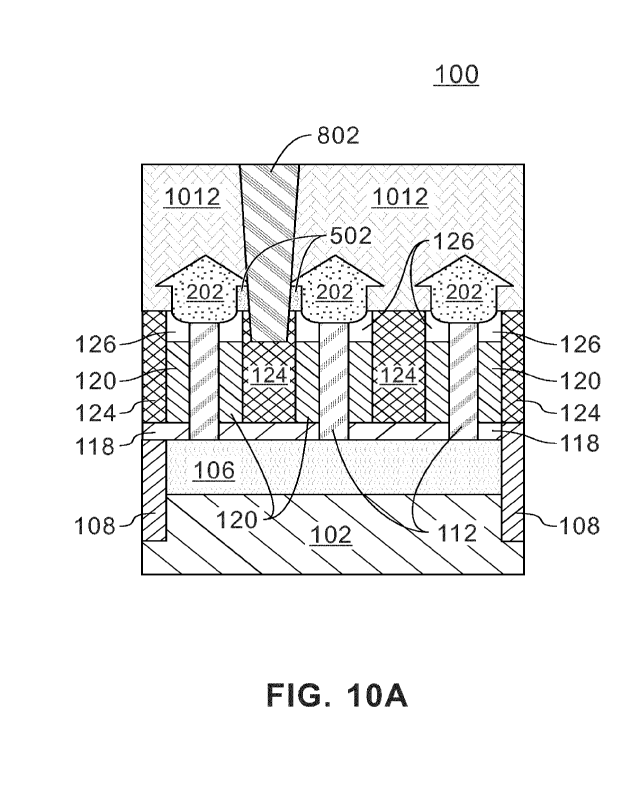
[0072] Referring now to FIG. 10A, a cross-sectional view of the semiconductor
structure 100 after middle-of-line
(MOL) contact metallization is shown, according to an embodiment of the
present invention. In this embodiment,
FIG. 10B is a lateral view of the semiconductor structure 100 taken along the
Y-axis.
[0073] As illustrated in the figure, top source/drain contacts 1012 (i.e., CA
contacts) extend all the way through
the top S/D/ region 202 while bottom source/drain contacts 1014 (i.e., CR
contacts) extend all the way through the
bottom S/D region 106. The process of forming metal contacts is standard and
well-known in the art. Typically, the
process includes patterning bottom S/D (CR) and gate contact trenches (CB)
followed by filling trenches (i.e.,
second recesses 930 of FIGS. 9A-9B) formed in a dielectric layer such as the
second ILD layer 802 and/or the first
ILD layer 124 with a conductive material or a combination of conductive
materials to form the top source/drain
contacts 1012, bottom source/drain contacts 1014, and gate contacts 1016. The
conductive material filling the top
source/drain contacts 1012, bottom source/drain contacts 1014, and gate
contacts 1016 includes a conductive
metal, for example, aluminum (Al), platinum (Pt), gold (Au), tungsten (W),
titanium (Ti), cobalt (Co), ruthenium (Ru),
copper (Cu), or any combination thereof. It should be noted that, in some
embodiments, an adhesion metal liner
(not shown) may be used before conductive metal depth, such as TiN, TaN, etc.
The conductive material may be
deposited by a suitable deposition process, for example, CVD, PECVD, PVD,
plating, thermal or e-beam
evaporation, or sputtering. A planarization process such as CMP is generally
performed to remove any conductive
material from surfaces of the semiconductor structure 100.
[0074] As can be appreciated in FIG. 10B, according to an embodiment, the top
S/D contacts 1012 have a
positive tapering profile (i.e., top critical dimension (CD) is smaller than
bottom CD) while bottom S/D contacts 1014
and gate contacts 1016 have a negative tapering profile (top CD is larger than
bottom CD). As known by those
skilled in the art, tapering includes a gradual thinning or narrowing towards
one end. In the case of the top S/D
CA 03194548 2023- 3- 31
WO 2022/128268 12
PCT/EP2021/081298
contacts 1012 having a positive tapering angle in a direction towards the top
S/D region 202, the thinning occurs in
an opposite direction to the (epitaxial) top S/D region 202 while the widening
occurs in a direction towards the top
S/D region 202. In the case of the bottom S/D contacts 1014 and gate contacts
1016 having a negative tapering
angle, the thinning occurs towards the (epitaxial) bottom S/D region 106 and
the high-k metal gate stack 120,
respectively. The different contact tapering profiles, may help avoiding very
small separations happening at the
same location (e.g., if all contacts are negative tapered, top CDs are
largest, increasing the risk of having contact
shorts at top S/D).
[0075] According to an embodiment, the top S/D contacts 1012 are formed
wrapping around the top S/D region
202. Stated differently, the above steps allow for the conductive material
forming the top S/D contacts 1012 to
surround or enclosed a larger surface of the top S/D region(s) 202 (including
sidewalls and bottom areas of the S/D
epi surface).
[0076] It should be noted that a portion of the protective liner 502 remains
in direct contact with a bottom portion
of the top S/D region 202. Specifically, the protective liner 502 remains at
an interface between the bottom portion
of the top S/D region 202, top surfaces of the top spacer 126 adjacent to the
top S/D region 202 and portions of the
second ILD layer 802 located between two consecutive top S/D region(s) 202. As
can be appreciated in FIG. 10B,
the remaining portion of the protective liner 502 is disposed on opposing
bottom sides of the top S/D region 202
(indicated by the circled region), by doing this over etching of the first ILD
layer 124 between adjacent top S/D
regions 202 does not expose the top S/D region 202, thus avoiding contact
shorts and improving device reliability.
[0077] The descriptions of the various embodiments of the present invention
have been presented for purposes of
illustration, but are not intended to be exhaustive or limited to the
embodiments disclosed. Many modifications and
variations will be apparent to those of ordinary skill in the art without
departing from the scope of the described
embodiments. The terminology used herein was chosen to best explain the
principles of the embodiments, the
practical application or technical improvement over technologies found in the
marketplace, or to enable others of
ordinary skill in the art to understand the embodiments disclosed herein.
[0078] In a preferred embodiment of the present invention, there is now
provided a method of forming a
semiconductor structure, the method comprising: forming a top source/drain
region in contact with a top surface of a
channel fin extending vertically from a bottom source/drain region located
above a substrate, a top spacer
separates the top source/drain region from a high-k metal gate stack located
around the channel fin, the channel fin
and the top spacer are in contact with an adjacent first interlevel dielectric
layer located directly above the bottom
source/drain region; recessing the first interlevel dielectric layer to expose
a top portion of the top source/drain
region and top portions of the top spacer adjacent to the top source/drain
region; selectively removing the exposed
top portions of the of the top spacer to expose a bottom portion of the top
source/drain region; and conformally
depositing a protective liner above and in direct contact with the top
source/drain region. Preferably, the method
further comprises: depositing a sacrificial material above the protective
liner; depositing an organic planarization
CA 03194548 2023- 3- 31
WO 2022/128268 13
PCT/EP2021/081298
layer above the sacrificial material; and recessing the organic planarization
layer, the sacrificial material, the
protective liner and a top portion of a first interlevel dielectric layer. A
portion of the protective liner preferably
remains at an interface between the bottom portion of the top source/drain
region, the top spacer adjacent to the
top source/drain region and a second dielectric material between two
consecutive top source/drain regions. The
recessing preferably creates first recesses with a positive tapering angle
widening in a direction towards the top
source/drain region and second recesses with a negative tapering angle
narrowing in a direction towards the high-k
metal gate stack and in a direction towards the bottom source/drain region.
The method preferably further
comprises: forming a top source/drain contact within the first recesses with
the positive tapering angle, the top
source/drain contact surrounding a surface of the top source/drain region. The
method preferably further comprises:
forming a bottom source/drain contact in at least one of the second recesses
narrowing in the direction towards the
bottom source/drain region. The method preferably further comprising: forming
a gate contact in at least one of the
second recesses with the negative tapering angle narrowing in the direction
towards the high-k metal gate stack.
The protective liner preferably comprises titanium nitride. Recessing the
first interlevel dielectric layer is preferably
performed using a high selectivity blanket atomic layer etching.
CA 03194548 2023- 3- 31