Note: Descriptions are shown in the official language in which they were submitted.
CA 03195681 2023-03-16
WO 2022/179719 PCT/EP2021/075551
- 1 -
Advanced heterofibrous monolithic wafer-like silicon anode
The present invention relates to advanced, ex-situ (before cell assembly), pre-
lithiated
negative electrode (body) based on group IV semiconductors according to claim
1. The
inventive silicon anode as an alkali-ion battery and preferably to a lithium-
ion second-
ary battery exhibits self-standing and/or heterofibrous and/or wafer-like
and/or mono-
lithic structures with high degree of structural ordering. This invention
offers the possi-
bility to engineer thick silicon electrodes featuring tailored weak and rigid
points in its
structures to buffer the volumetric expansion during charge/discharge cycles
in a pre-
dicted manner, overcoming the uncontrolled volumetric expansion in the state
of art
silicon anodes.
CA 03195681 2023-03-16
WO 2022/179719 PCT/EP2021/075551
- 2 -
Definitions of the invention are given after the "object of the present
invention" for each
aspect of the inventive anode.
From US20180331341A1 a spun silicon-based mat is known made from a mixture of
a liquid silicon precursor and polymer, wherein lithium is introduced in the
silicon matrix
of the resulting nanotubes of the spun mat.
Due to the rapid growth of e-mobility sector together with portable smart
electronic
equipment, there are growing demands for advanced secondary batteries with
higher
energies as well as high charge rate acceptance which address the actual
challenges
originated from the users of BEV battery powered electric vehicles which
request much
higher operation radius on single charge and shortest charging time possible
defined
here as 5 30min from 15% SoC to 100% SoC (State of charge) with negligible
negative
effect on the cycle life defined as SoH (state of health) - The SoH indicates
the ratio of
the currently maximum usable capacity to the nominal capacity.
Li-ion battery with high cycle life and high charge rate acceptance is in
direct conflict
at least with the present types of alkali-ion anodes which are mostly based on
Li+ in-
tercalation reaction into graphite. The slow Li+ diffusion on intercalation
into graphite
together with the presence of concentration polarization gradient further
restrict acces-
sibility of Li+ by hampering the transport rate of Li+ from electrolyte to
anode. This
phenomenon then exceeds Li diffusion-intercalation rate and induce
accumulation of
more charge carriers on the anode surface and drives the anode potential below
0 V.
This is the area where lithium plating is kinetically more favorable than Li+
intercalation
reactions and as the working potential of graphite is close 0.1V a metallic Li
deposition
occurs and subsequently cell degradation and safety issues.
The growing sector of portable electronic device, recently, coinciding with
the trend
towards "small" and "compact" energy carriers hereby defined as batteries with
desired
high (>750 Wh/l) volumetric energy density, and "light" defined as batteries
with desired
high (>300 Wh/kg) gravimetric energy density are fulfilled by the inventive
anode.
There is mismatch in understanding the definition of "high energy battery"
terminology
CA 03195681 2023-03-16
WO 2022/179719 PCT/EP2021/075551
- 3 -
where the most preferable demand to the battery is to have high gravimetric
energy in
Wh/kg. But in reality, its opposite a volumetric capacity Wh/1 is more
demanding due
the fact that available space: As example serve the available space/volume for
inser-
tion of battery into the smartphone, notebook or in electric car platform, for
which the
most limiting factors is the need of battery with both high volumetric and
gravimetric
energy density hereby defined as compact & lightweight battery.
Silicon as is one of the most promising type of anode for the post-lithium
batteries
which are based on alloying redox reactions with theoretical room temperature
gravi-
metric/volumetric capacity in de-lithiated (discharged) state 3579 mAh/g, 8334
mAh/cm3 and lithiated Li3.75Si (charged) state 1857 mAh/g, 2193 mAh/cm3, while
average discharge potential of 0.4 V vs. Li/Li+. Compared to the most common
type of
anode ¨ graphite hereby defined as state-of-the-art anode used in commercial
Li-ion
cells - is defined as gravimetric (graphite) 372 mAh/g vs. (silicon) 3579
mAh/g and
volumetric (graphite) 837 mAh/cm3 vs. (silicon) 8334 mAh/cm3 capacity.
Lithium metal anode volumetric capacity in fully discharged state is 0 mAh/cm3
so all
lithium was stripped down from e.g., a Cu foil during discharge and
transferred towards
the cathode. So, lithium in fully charged state has a capacity of 2061 mAh/cm3
com-
pared to silicon which has in fully discharged state a capacity of 8334
mAh/cm3 and
fully lithiated ¨ charged state 2193 mAh/cm3. So those numbers disclose
advantages
of using lithiated silicon anode instead of LMA (lithium metal anode). This is
because
theoretical volumetric fluctuation of lithium metal is 100% represented by
average
0.205 mAh/cm2 per 1 micron of thickness. Thus, a LMA anode is dimensionally
unsta-
ble. So, on discharging (stripping) the thickness of lithium metal foil
decreases where
opposite on charging (plating) increase. In comparison to graphite which is
the most
commonly used anode material, all volumetric fluctuations during cycling of
the in-
ventive anode are compensated inside the internal voids/porosity (-,30% of the
vol-
ume) of anode with only minor changes of anode thickness.
CA 03195681 2023-03-16
WO 2022/179719 PCT/EP2021/075551
- 4 -
LMA foil is a host-less anode. Thus, in order to charge it large irreversible
losses are
present due the SEI (solid electrolyte interphase) formation, but the most
important
factor is a lithium defragmentation and subsequently expansion of SEI layer
which is
even for use of advanced electrolytes 50% and progressively increasing on each
cy-
cling (lithium consuming). So totally the minimum theoretical volumetric
fluctuation for
LMA is now in best case scenario 150% vs. 276% for silicon but the real
situation is
different. LMA (foil) is preferably used in excess due to the Li+ consuming
SEI build-
up during cycling. So, when all available Li+ is consumed the cell is dead.
In order to deal with cycle life in realistic Li-ion batteries with LMA
commonly used
excess is 200%. So, the comparison of the theoretical volumetric capacity of
silicon
2193 mAh/cm3 with the best possible scenario LMA foil with only 100% excess
results
in a reduction by a factor of 2 to a theoretical capacity of 1031 mAh/cm3.
Because
thereof, lithium excess within the anode/cell compartment represents dead
weight/vol-
ume, its excess in battery is mainly because to compensate its consumption and
en-
hance cycle life. Now when we compare realistic LMA anode 1031 mAh/cm3 with
graphite and its volumetric capacity of 837 mAh/cm3 it's clear that if we add
expansion
contribution from SEI on LMA 50%, it's evident that using claims like "lithium
metal is
holy grail of battery" it's just lack of understanding of the basic
electrochemistry and
cell-battery-module-pack-system.
Important factor for the solid-state battery with LMA anode is a necessity of
use specific
device capable to provide uniaxial pressure over the battery module. This is
because
LMA is dimensionally unstable so in order to exchange ions lithium metal foil
needs to
be pressed against solid electrolyte which then results to additional dead
weight/vol-
ume gain. However, this time not from the cell components but due the
additionally
auxiliary components related to battery module or pack and because of stack In
order
to distribute forces such as 10 MPA homogeneously over the entire surfaces.
There-
fore, a realistic cell design would result in a further decreased energy
content of around
18% and also significant safety concern due the presence of pre-compressed
battery
CA 03195681 2023-03-16
WO 2022/179719 PCT/EP2021/075551
- 5 -
modules within e.g., an electric car which during crash accident could release
extreme
energies present in such batteries.
In the scope of the previous analysis the inventive ex-situ pre-lithiated
heterofibrous
silicon anode with preferably an artificial SEI layer, having mixed ion-
electron conduc-
tivity is a new and viable solution for the next generation batteries, capable
to accept
high charge rates and realize ultra-compact batteries with capacities over
1200 Wh/1
and 350 Wh/kg with Li-rich LLS cathode.
It's clear that the higher density of silicon would offer 10 times higher
volumetric energy
content than graphite anodes, but for the cost of high volumetric expansion on
lithiation
defined as (graphite) 11.2% and (silicon), 276% where the challenge is the
nature of
silicon expansion. (See ELSEVIER Journal of Industrial and Engineering
Chemistry,
Journal Volume: 74, Journal Issue: 25; Journal ID: ISSN 1226-086X page number
216-
222). This is a highly anisotropic process so the point of
interaction/entering of elec-
trons/ions into reaction with silicon and subsequently alloying reaction
proceed differ-
ent from the traditional intercalation type anode ¨ graphite.
The low cost of silicon as second most abundant element in the Earth's crust
(about
28% by mass) after oxygen in combination with high volumetric/gravimetric
energy of
Si offers significant benefits towards the use in next generation energy
carriers ¨ bat-
teries. Si is a group IV type semiconductor with conductivity of 1.6x10⁻³ S/m
and Li+
diffusivity of 1.9x10⁻¹⁴ cm2/s, but the Li-'- diffusion in Si proceeds by
different speeds
according to the Si crystal orientation and thus the direction is 3D. While
the critical
force (1) in <100> and <111> orientation is about 40% and 15% lower than in
<110>),
which means that lithium atoms have a preferred diffusion rate in <110>
direction.
Thus, this discrepancy in diffusion would result in fast capacity degradation
due the
non-uniform anisotropic expansion/contraction of the silicon at particle level
and sub-
sequently on electrode. This results in different rates of lithiation within
the internal
electrode structures, where e- conduction paths are provided dominantly by
physical
interaction between active mass Si, binder and conductive additives. The
points of Si
CA 03195681 2023-03-16
WO 2022/179719 PCT/EP2021/075551
- 6 -
interaction with Li+ and e- would define the reaction kinetics and thus as Si
anode
cycling proceed by repeatable charge/discharge cycles, the position of Si
particles
within the present anode structures isn't rigid. Therefore, each
shrink/expansion on
subsequent cycling will redistribute internal ion/electron conduction paths
which is due
the presence of polymeric binder flexible. Thus, the point of interaction of
silicon with
e- always changes due the complex nature of slurry-based Si anode where active
Si
particles must interact with binder and conductive additives to create an
electron and
ion conduction path.
Present technological solutions of the silicon-based anodes are based on using
Si as
minor additive into existing slurry-based anodes where internal porosity of
the anode
is used to compensate volumetric fluctuation during cycling. Because of
existing limi-
tation originated from the preferential usage of slurry-based anode such
volumetric
changes are only partially compensated by internal voids of the anode, at
which the
most of the pressure build up within the anode is converted into mechanical
forces.
This further destabilizes structural connection between Si-graphite-binder-
conductive
additives. In a traditional silicon-based Li-ion batteries e- conduction path
is provided
by the interaction of silicon with billions of conductive nanoparticles which
transport e-
to and from the electrode. Because a morphological change of silicon-based
anode
occurs there isn't a steady state Li-Si alloying point. So, the direction from
which lithium
will enter into crystallographic structure of silicon while forming amorphous
LixSi phase
and the presence of local Si anisotropy will further result in deformation and
subse-
quently redistribution of mechanical forces and finally cracking and
delamination of Si
structures. The Si surface is therefore exposed to the electrolyte and further
consumes
available electrolyte and Li+ to create a new SE! layer(s). This leads to
irreversible
capacity loss as well as impedance gain, resulting in evolving of excessive
heat during
cycling, whereby the most limiting factor is fast charging rate (Solid
Electrolyte Inter-
phase layer).
To solve the above mentioned problems, it is an object of the present
invention to
provide a negative electrode ¨ heterofibrous, lithiated silicon anode
preferably
CA 03195681 2023-03-16
WO 2022/179719 PCT/EP2021/075551
- 7 -
exhibiting hierarchical electrode porosity, for an alkali-ion battery
exhibiting an signifi-
cantly improved cycle life, high coulombic efficiency, gravimetric and
volumetric energy
density, active mass utilization level and innovative production methods
characterized
as preferably solvent-free and/or binder-free and/or drying-free and/or slurry-
mixing &
degassing-free and/or slurry coating-free and/or anode current collector foils
to tab
welding-free and/or calender-free anode (and process of preparation) which
together
brings a high energy, cost efficiency and environmentally positive effect of
such ad-
vanced silicon anode. High charge rate acceptance of heterofibrous, preferably
aniso-
tropically, lithiated, (preferably n-type) silicon wafer anode defined here at
cell level as
full charge of cell from 15% SoC to 100% SoC in preferably 512min would have
global
impact on the alkali-ion battery market. (Monolithic) Wafer may mean: self-
standing
and/or heterofibrous and/or silicon (or in general group IV semiconductor)-
based an-
ode and/or unified anode body made from heterofibrous silicon material having
prefer-
ably tailored hierarchical open porosity.
Self-standing may be understood as a structural property. Such anode is
capable of
keeping its structure without external support such as an external backbone
that only
serves structural rigidity purposes and would take away space in the anode
which
could otherwise be used for the active material. Just as it is expected from a
wafer.
The term "heterofibrous" fibers refers to a possible variation in length
and/or diameter
of the same.
Monolithic may refer to the shape and/or structure of the active anode
material made
from layers of fibers by fusing them together in the inventive way which
results in a
unified active anode material body.
The task is solved according to the present invention by an anode according to
claim
1.
The inventive negative electrode may be used in an alkali-ion rechargeable
battery and
comprises an electrochemically active material of the anode wherein the active
CA 03195681 2023-03-16
WO 2022/179719 PCT/EP2021/075551
- 8 -
material is selected from the Group IV semiconductors and/or the active
material is
provided as a heterofibrous and/or wafer-like and/or self-standing and/or
monolithic
anode body and/or the anode body comprises at least 2 (individual/discrete)
layers of
aligned and/or stacked and/or interlaced fibers and/or the at least two layers
are ar-
ranged parallel on top of each other and/or the layers are interconnected at
multiple
discrete interconnection sites, preferably interconnection points, via
metallurgical
bonds and/or the metallurgical bonds comprise or consist of Li-Group-IV-
semiconductor-alloy and/or lithium or a mixture of the two and/or the discrete
intercon-
nection sites are distributed across the anode body, preferably discretely
distributed
over the, more preferably whole, area of the layers and/or the metallurgical
bonds ex-
tend in an out-of-plane direction with respect to the individual layers and
are spacers
between the layers, and the anode body, in particular its layers, is/are
preferably une-
venly lithiated with non-lithiated, deficiently lithiated and
stoichiometrically lithiated ar-
eas.
The inventive electrode may also be described as a negative Li + host type
alloying
electrode.
The present invention may also refer to an anode comprising at least 2
(individual/dis-
crete) layers of aligned and/or stacked and/or interlaced fibers wherein the
at least 2
layers are arranged parallel on top of each other wherein the layers are
interconnected
at multiple discrete interconnection sites, preferably interconnection points,
via metal-
lurgical bonds, wherein the metallurgical bonds comprise or consist of Li-
Group-IV-
semiconductor-alloy and/or lithium or a mixture of the two wherein the
metallurgical
bonds extend in and out of the plane direction with respect to the individual
layers and
are spacers between the layers, the gaps between the layers formed by the
spaces
can be filled with the silicon-lithium alloy formed during charging/lithiation
of the anode,
wherein the anode comprises an SEI-layer the volume/extension of which is
adapted
to the volume of the anode in the maximum lithiated state. Such SEI-layer may
be
formed by over lithiation of the anode and subsequent formation of an
artificial SEI-
layer via dopants or electrolytes which consumes the excess of lithium
(preferably from
about Li21Si5 to about Li15Si4) while the silicon lithium alloy has its
maximum volume.
CA 03195681 2023-03-16
WO 2022/179719 PCT/EP2021/075551
- 9 -
Thereby, the SEI-layer does not experience forced expansion during charging of
an
according battery with such anode.
In the scope of our invention, we apply an innovative method for the producing
of ex-
situ pre-lithiated silicon structures of higher order ¨ monolithic
heterofibrous anode
which allow to finely tune the content of lithium within the silicon anode
active material
to suit lithium free or lithiated cathode. Since all subsequent processes are
applied at
the wafer (anode active material body) level, all irreversible losses
originated from SEI
forming is compensated internally by ex-situ method.
Unevenly distributed lithiation or anisotropic lithiation of the layers
comprise non-lithi-
ated, deficiently lithiated and stoichiometrically lithiated areas.
Spot-fusing, which may also be called interconnection sites as a synonym,
means met-
allurgical bonds from Li-Group-IV-semiconductor-alloy and/or lithium or a
mixture of
the two, the layers are interconnected at multiple discrete points by the
metallurgical
bonds and the discrete points of interconnection are spread across the anode
body,
hence over the whole area of the layers.
According to the present invention discrete may mean separated from each other
or
individually introduced or having space between them or a combination the
same.
Interconnection sites are located between the layers and may extend into the
layers
for improved anchoring.
Spot-fusing at certain positions may additionally guide the subsequent
distribution of
LixSi(y) in the anode during cycling controlling the way how LixSi(y) will
redistribute in the
anode. The mechanical stress coming from cycles of lithiation and de-
lithiation charg-
ing/discharging can therefore be distributed.
"Anisotropy" is a way how the deposition of Li in the anode as LixSi(y) can be
predicted
and guided during further repeating charging/discharging cycles. It's like
chassis of
modern car in which structure engineers insert weak spots which will guide
during an
CA 03195681 2023-03-16
WO 2022/179719 PCT/EP2021/075551
- 1 0 -
accident how the chassis will deform and absorb the energy from the crash. The
spot
fusing may do the same inserting weak spot into structurally rigid LixSi anode
body.
The metallurgical bonds are preferably introduced by electrochemically induced
Li fus-
ing or introduction of molten lithium. Locations, distribution, shape, size
and numbers
of those fused spots can be extracted from the analysis of current
distribution non-
uniformity within LixSi(y) anode. Techniques for the current analysis include
galvanos-
tatic, potentiostatic and impedance spectroscopic measurement techniques.
Further-
more, the distribution of the fused spots can be derived via in-situ and/or ex-
situ imag-
ing techniques like scanning electron microscope and transmission electron
micros-
copy, whereby elemental mapping via energy-dispersive X-ray spectroscopy eluci-
dates the location of metallurgic bonds and the presence of density gradients.
Tortuosity of the anode is directly linked to the accessibility of the
straightest and short-
est possible electron and ion conduction paths established for Li+ by
electrolyte pre-
sent within the internal voids of electrode and for e- direct physical
interaction of active
mass with conductive additives such as carbon black or conductive polymers
and/or
its combination with. Traditional slurry-based electrode lack of structural
ordering which
is crucial for obtaining efficient electron and ion paths while monolithic
silicon anode
with high degree of structural ordering defined as hierarchical structure.
This consist
from layers of aligned silicon fibers stacked into the monolithic anode
structure and is
therefore able to establish efficient paths. Monolithic silicon anode with
ordered poros-
ity replaces traditional mediated electron conduction paths characteristic for
slurry-
based electrodes which are based on direct physical contact between silicon,
conduc-
tive agents, binder and current collector foil by the inventive direct lithium-
fused fibrous
low resistive heterofibrous silicon anode body. This type of open structure
allows fast
charging of the anode beyond the critical limit of the existing intercalation
type anode
present at 80 % SoC.
The artificial SEI layer may be made by the following steps.
CA 03195681 2023-03-16
WO 2022/179719 PCT/EP2021/075551
-11 -
Interconnected layers of Si-fibers are lithiated (over lithiated) to Li21Si5.
Such lithiation
may be conducted under elevated temperature preferably above 100 C under a pro-
tective solvent such as e.g., linear, branched or cyclic alkanes (Adv. Energy
Mater.
2019, 1902116; DOI: 10.1002/aenm.201902116). Suitable solvents may be binary
and
or ternary mixtures of polar and non-polar solvent or solvents where more
preferably
non-polar solvent is hydrocarbon such as decane and polar solvent with boiling
point
> 130 C such as DEGDME diethylene glycol dimethyl ether.
The (over) lithiated Si-layers are then treated with dopants to form an
artificial SEI
layer, preferably in a maximum lithiated stated of the Si-anode. The reaction
of the
dopants with the lithiated anode reduces the lithium content. A stoichiometry
of Li15Si4
may be reached by/after artificial SE! formation which is stable at room
temperature.
Since the SEI layer is induced artificially after the lithiation of the Si-
Anode the aSEI
layer has less imperfections (cracks, weak spots, thickenings,...) since there
is only
SEI formation at the end of the initial lithiation process and hence no volume
expansion
happens after SE! formations occurs (as it is the case if SE! is formed before
or during
initial lithiation process). The protective solvent prevents formation of the
thick SE!
layer at an earlier stage of/during lithiation.
SEI formation may be conducted in the protective solvent into which
liquid/dissolved
and/or gaseous dopant (e.g. As-, P-, (H)F-compounds) such as group V
pnictogens or
low concentration electrolyte are introduced alternatively or additionally the
SEI-layer
may be introduced by reaction of the over-lithiated Li21Si5 with an
electrolyte such as
used in a final battery. Such electrolytes may be chosen from e.g., ceramic
solid elec-
trolytes, polymer electrolytes, ionic liquids as known to the person skilled
in the
art. Upon contact of the dopant and/or electrolyte with the (over) lithiated
Li21Si5, lithium
reacts with the dopant and/or electrolyte forming a tailored (artificial) SE!
layer contain-
ing e.g., Li3P, Li3As, Li4As and/or LiF depending on the used dopant and/or
electrolyte.
After consuming part of the Li from Li21Si5 by reaction with dopant and/or
electrolyte
and/or dopants and/or electrolytes room temperature active alloy (such as
Li15Si4) re-
mains as a capacity of the Anode. The resulting artificial SE! layer
experiences mixed
CA 03195681 2023-03-16
WO 2022/179719 PCT/EP2021/075551
- 12 -
ion-electron conductive properties. The amount of Dopant in the Si-Layer can
be
adapted to the amount of Li present in the Li21Si5 to yield the desired
Lithiation degree.
This method reduces the loss of Li during the initial formation of the SEI
layer compared
e.g., to the classical lithiation of the final battery by initial charging.
Furthermore, since
the SEI is formed when the LixSi(y) species, such as Li21Si5, has his higher
volume, no
crack of the SEI can occur by the volume expansion of the silicon, which is
more often
the case during silicon anode operations
Common Li-ion cells contain a certain amount of lithium inserted/intercalated
into NMC
cathode which means that battery is in fully discharged state where all
lithium is at the
cathode side. In order to move Li + from the cathode into the anode, the anode
needs
initial charging, however during this process, a high irreversible loss of Li
takes place.
This Li is consumed by the SEI buildup as a non-active part of the SEI layer
and be-
cause of the high reactivity of lithium, thick highly resistive RsEI) is
formed. In additional,
this affects the Rd high charge transfer resistance (kinetics of
electrochemical reac-
tion). This common in-situ process uses only Li which is present in the cell
as part of
the energy storage matrix. In case of a Si-anode the lithiation is done in-
situ such as
by mixing of suitable Li precursor capable to be part of the slurry or to be
sprayed over
the surface of electrode to be lithiated and subsequently activated by
calendaring,
cracking the protective layer of SLMP as
"2010 DOE Vehicle Technologies Pro-
gram Review" P.I. Marina Yakovleva Co-P.I. Dr. Yuan Gao FMC June 8th, 2010
(https://www.energy.gov/sites/prod/files/2014/03/f11/es011 yakovleva 2010
o.pdf).
However, the in-situ lithiated electrode will lead to a super expensive
method, since
building a protective layer over the micronized lithium metal powder
introduced ex-situ
during cell assembly but has to be activated subsequently.
In contrast the preferred ex-situ introduced lithium which was supplied
externally can
be a. provided in excess, therefore allowing to achieve 100% of the
theoretical cell
capacity and b. provide a uniform SEI layer with little to none cracks, weak
spots, thick-
enings, etc. since formation of the SEI layer is conducted in a maximum
expanded
CA 03195681 2023-03-16
WO 2022/179719 PCT/EP2021/075551
- 13 -
state (by volume) i.e. (over) lithiated state of the anode - Li21Si5. This
method may also
avoid inclusions of SEI layer material inside the LixSi(y) body.
Traditionally existing silicon-based anodes are based on intrinsic silicon
where nano-
particles have various shapes such as OD, 1D or more complex 3D host
structures for
silicon or micro-meso porous 3D silicon or etched silicon anode body. Where
for OD
silicon particles having under critical diameters which prevents particles to
rupture dur-
ing lithiation (expansion) is having protective carbon coating on its surfaces
where such
coating is more preferably carbon. This type of protective coating represent
barrier for
lithium initiated self-fusing of surrounding silicon structures in close
physical contact.
Whereas traditional silicon anodes protective coating based on partial
oxidation of the
surface of silicon and or carbon coating those processes are applied to deal
with pyro-
phoric nature of nano-sized silicon particles and ability to be processed as
slurry with
suitable solvent without significant side reaction. The presence of barrier
layers be-
tween silicon particles in slurry-based electrode doesn't allow lithium to
efficiently prop-
agate self-fusing process over the full electrode. Slurry based silicon
electrodes keep
their internal electron conduction paths dominated by physical contacts
between active
mass particles ¨ silicon and surrounding particles, conductive additives such
as 1D
shape as CNT and or OD as carbon black and polymeric binders where our
invention
of heterofibrous anisotropically pre-lithiated monolithic silicon anode use
preferably ad-
vantageous lithium initiated self-fusing process of silicon to build
innovative fully inter-
connected monolithic 3D (wafer-like) anode. Preferably physical contacts
mediated by
conductive additives and polymeric binders typical for slurry-based silicon
anode are
completely eliminated by (full) metallurgical bonds/joints created by fusing
lithium with
cross-contacted silicon fibers and/or where pre-lithiation, artificial SEI
(Fig. 13)
In an embodiment an object of the invention is an engineered hetero-fibrous
and/or
monolithic silicon anode body with functional anisotropy represented by the
introduc-
tion of specific areas (fig. 7) into the monolithic silicon body which further
comprises
combinations of structurally rigid (fused parts of the lithiated layers) and
weak spots
(non-lithiated and or partially lithiated and or fully lithiated and/or over-
lithiated parts of
CA 03195681 2023-03-16
WO 2022/179719 PCT/EP2021/075551
- 14 -
the layers). They together may form an engineered electrode superstructure
capable
to re-distribute volumetric fluctuation of silicon by allowing weak areas to
absorb and
redistribute it. Those areas may preferably be oriented in plane of electrode
to accom-
modate volumetric changes and re-distribute it, preferably according pre-
defined direc-
tion where rigid spots are preferably oriented out of plane and interconnect
silicon lay-
ers. The diameter of the fused spot or line is preferably in the range of 1 to
1500 pm,
more preferably in the range of 375 pm. The outer-side distance of the fused
spots or
lines is preferably in the range of 50 to 3000 pm, more preferably in the
range of 750
pm, whereby the fusing spots and/or lines may feature a certain geometric
pattern
(spiral, star-shaped, hexagonal, etc.) and/or an uneven distribution.
The fused spots may be provided as part of the structural integrity of the
(wafer-like)
stack of layers of Si-fibers. Thus, the number of fusing spots may be chosen
accord-
ingly to provide for at least an initial support of the overall anode
structure. Anisotropic
lithiation may be provided by the above stated discrete lithiation process,
since Lithia-
tion is oriented within and/or between the provided layers and is therefore
provided
with a defined plane and direction of extension. The spots may also add high
degree
of structural strength and partial flexibility to deal with silicon anisotropy
on cycling.
Additionally, to the (anisotropic) fusing spots fig. 7 preferably an
anisotropically aligned
Si-Li alloy-pattern is provided on and within the (wafer-)structure/layer
structure/Si-fi-
bers with preferably lithiated parts distributed over the total anode body
(wafer)/layer
structure and non-lithiated or Li deficient parts in the first process step
distributed over
the total anode body (wafer)/layer structure at the same time (see fig. 2 for
example).
Such alignment may also be called functional anisotropy by lithiation and
forming Li-Si
alloy with structural aka. flexural modulus gradient between spot-fused
pillars. Lithia-
tion may generally be established by a print-fuse method with liquid lithium
and/or its
alloys and/or electrochemical lithiation and/or its combination where more
preferential
it's a two-step lithiation.
Spot-fused may mean:
CA 03195681 2023-03-16
WO 2022/179719 PCT/EP2021/075551
- 15 -
O the layers are interconnected at multiple discrete points by metallurgi-
cal bonds and/or
o connected in individual single places and/or areas and/or lines
O at the discrete points of interconnection Li-Group-IV-semiconductor-
alloy and/or lithium or a mixture of the two is provided as the metallur-
gical bond material, and/or
o the discrete points of interconnection are distributed across the anode
body, hence over the whole area of the layers and/or
O the layers are spaced apart from each other, preferably by the material
of the discrete points of interconnection and/or
o the metallurgical bonds extend in an out-of-plane direction with re-
spect to the individual layers,
the meaning of spot-fused goes beyond a mere connection in single dots and may
also
include lines and/or areas and/or pillars. Those may have the properties as
outlined in
thus patent application.
According to a preferred embodiment distribution or degree of lithiation
within the lay-
ers varies, wherein the degree of lithiation of the anode body cross to the
plane of
extension of the layers is similar
According to an embodiment the present invention is directed to a negative
electrode
for the use in an alkali-ion rechargeable battery, wherein the
electrochemically active
material of the anode is selected from the Group IV semiconductors. The active
mate-
rial may be provided as a heterofibrous and/or wafer-like and/or self-standing
and/or
monolithic anode body. The anode body comprises at least 2 layers of aligned
and/or
stacked and/or interlaced fibers which are spot-fused together by the presence
of lith-
ium at multiple discrete points of their physical contact forming individual
Li-Group-IV-
semiconductor-alloy (e.g., LiSi-alloy) bonds between the layers.
Alternatively, or addition-
ally to the spot fusing the anode body, in particular the layers, are
anisotropically lithi-
ated. The spot fusing may at least in one aspect of the present invention
represent at
least a part of the anisotropic lithiation. The anode as mentioned above may
contain
CA 03195681 2023-03-16
WO 2022/179719 PCT/EP2021/075551
- 16 -
an excess of lithium, at least in a charged state, within the anode body which
may not
necessarily be involved in the bonding of the layers. This additional lithium
may be
present as e.g., charge carrier, preferably within the individual layers.
It is an objective of the invention to introduce an innovative method how to
efficiently
deal with the volumetric fluctuation of the silicon-based anode by introducing
strategi-
cally positioned weak and rigid spots - structures which together work in
synergy. This
might be visualized in a similar manner as structural weak spots originally
placed into
chassis of a car by engineers to save life by absorbing impact forces during
auto-crash
and convert it into mechanical deformation of the chassis and surrounding
structural
parts of car. Weak spots may also be called expansion/shrinkage zones into
which the
anode material may expand during the lithiation (charging) and shrink on de-
lithiation
(discharging).
It is a preferred objective of the invention to introduce structural and/or
material anisot-
ropy represented by a variation of anode density caused by lithiation (and/or
lithium
alloy formation) in the heterofibrous silicon anode body (wafer) and/or
electrical ani-
sotropy represented by the conductive (lithium, lithium alloy) lines, dots,
areas, pillars
(in total hereby called pillars, see e.g. Fig. 2) pillars preferably oriented
perpendicularly
to the electrode base (to the direction of extension of the silicon fiber
layers).
In an embodiment an object of the invention is a production of well aligned
and/or
interlaced and/or stacked self-standing layers comprising (preferably
consisting of) sil-
icon nano or microfibers and or silicon nano or micro rods, thus crystalline
and/or amor-
phous and/or poly-crystalline silicon, preferably from suitable hydrogenated
silicon
precursors which are preferably liquids within the operating window of nano
and or
micro fibrous production apparatus, preferably defined between m.p. -55 C to
b.p.
420 C. Silicon precursors include, but are not limited to cyclic silanes
(SinH2n, where n
> 3) e.g. cyclohexasilane Si6H12, (m.p. +16.5, b.p. +226 C) or acyclic silanes
(SinH2n+2
where n>3) such as hexasilane Si6H14 (m.p -44,7 C to +b.p. 193.6 C). The
general
concept how to convert silanes into crystalline or polymer silicon and thus
fibers can
CA 03195681 2023-03-16
WO 2022/179719 PCT/EP2021/075551
- 17 -
be found e.g. in ACS Applied Materials and Interfaces, Journal Volume: 4;
Journal
Issue: 5, pages 2680-2685; Journal ID: ISSN 1944-8244 (solution-based
synthesis of
microcrystalline silicon). According to an embodiment, the Si precursor may
also carry
dopant and or dopants which is/are crosslinked with the Si precursor e.g.
forming a co-
polymerized Si/dopant solution prior to a fiber spinning process or growing Si
rods,
wires having nano and or micro dimensions.
The above and the following information of Si and Si-fibers are also meant to
apply to
any group IV semiconductor or a mixture of them.
A suitable liquid silicon precursor could also be poly(silanes) such as
dimethyl-pol-
ysilane (DMPS), deca-phenyl-penta-silane (DPPS) and poly-methyl-phenyl silane
(PMPS) and/or suitable n-type dopant could be phosphorus bromine PBr3.
A first possible method for the production of the silicon layer is electrospun
of a (poly-
meric) solution onto a substrate, and subsequent thermal decomposition by
means of
a heating treatment and/or laser treatment and/or microwave treatment, in
order to
obtain a silicon layer made from rods and/or wires having nano and or micro
dimen-
sions, which can be doped or not. The same operation is carried out by
electrospinning
a second layer of (polymeric) silicon precursor and subsequently thermally
decompo-
sition to obtain a second silicon layer. The operation can be repeated X times
to obtain
X stacked/interlaced silicon layers.
A second possible method is based on carbonaceous seed carriers decorated with
suitable catalyst (e.g., gold, silver nickel, etc.) capable to form
intermetallic compound
with silicon on the growing process. Those seed carriers are in the shape of
OD ((sili-
con)-nanocrystals, quantum dots) 1D (CNT) and/or 2D (graphene, mxenes, silicon
nanosheets) and/or 3D (reduced graphene oxide foam, MOF) carbon-based
materials.
Those seed materials decorated with the mentioned nucleation seeds may be
aligned
by dielectrophoresis at the top of a solution containing the co-polymerized
Si/dopant
mixture, which can be dissolved in hydrocarbon or mix of hydrocarbons, such as
par-
affin for example. A system of current collectors can be implemented in
different
CA 03195681 2023-03-16
WO 2022/179719 PCT/EP2021/075551
- 18 -
geometry, for example such as a hexagonal one, containing 3 cathodes and 3
anodes.
The alignment of these seed carriers will create an electronic percolation
network
which will short circuit the cathode/anode pairs. This short circuit will
create heat by
the Joule effect at the surface of the seed carriers, which triggers the
thermal decom-
position of the silicon precursor and a silicon layer made of rods and/or
fibers, and/or
wires having nano and or micro dimensions will be obtained. In addition, this
silicon
layers can be doped by various n-types (e.g., phosphorus) or p-type (e.g.
boron) via
addition of suitable dopant precursors (e.g. B2H6, pnictogenes, etc.) in the
precursor
solution. Several layers can be obtained by stacking up the dielectrophoresis
elec-
trodes in a hexagonal system by an electric insulator, in order to obtain a
stack of
electrodes.
The good production of the described anodes can be monitored by scanning
electron
microscopy to confirm the morphology of the silicon monolith, as well as micro
tomog-
raphy to ensure the good distribution and position of the fusing point.
Regarding the
performances of the anode, usual galvanostatic cycling method can be implement
as
well as cyclic voltammetry, where the anodic and cathodic peaks should be
included
in less than 0.2 V, translating the good kinetics of the electrochemical
reactions, and
thus an appropriate morphology of the silicon anode for ionic and electronic
diffusion,
as well as efficient charge transfer phenomena. As the ex-situ lithiated anode
(Li15Si4)
represents the fully charged state of an electrochemical half-cell based on
the fabri-
cated silicon anode with a suitable lithium free cathode e.g., sulfur, the
electrochemical
cell features an open circuit potential greater than 0 V, as for the example
sulfur a
potential of 2.1 V is observed. To monitor the full lithiation of the ex-situ
fabricated
Li15Si4 anode (e.g., of 100 mg) the initial discharge reaches the complete
theoretical
capacity (185 mAh in the case of a 100 mg Li15Si4 anode). The beneficial build-
up of
the ex-situ fabricated SEI is shown via repeated charging/discharging of the
such fab-
ricated anode without losing capacity due to the formation of lithium
consuming in-situ
SEI build up. The structural integrity of the ex-situ SEI in combination with
the aniso-
tropic lithiation results in a capacity retention of up to 90% of the initial
discharge
CA 03195681 2023-03-16
WO 2022/179719 PCT/EP2021/075551
- 19 -
capacity over up to 1,000 charge/discharge cycles at current densities 3 C.
Another
approach visualizing the anisotropic Li distribution is achieved via operando
analysis
of the charge distributions via X-ray microdiffraction during
charging/discharging, es-
pecially during the initial discharge (according to ACS The Journal of
Physical Chem-
istry Letters, Journal Volume: 1; Journal Issue: 14; Pages 2120-2123; Journal
ID: ISSN
1948-7185).
Another object is a spot-fusing of the resulting monolithic heterofibrous
silicon anode
e.g., initiated by the alloying reaction between lithium and/or binary lithium
alloy and or
ternary lithium alloy and or lithium salt. A suitable solvent for alloying Li
with Si and
capable to solubilize lithium salt where more preferably lithium salt is
LiTFSI and suit-
able solvents are e.g. binary and or ternary mixture of polar and non-polar
alkane sol-
vent where more preferably non-polar solvent is hydrocarbon such as decane and
po-
lar solvent is diethylene glycol dimethyl ether where boiling point of
solvents is higher
than 130 C and where molarity of LiTFSI within the electrolyte is 0.75 M where
more
preferably 0.25 M. Preferably pre-lithiation is introducing structural lithium
(e.g. Dots/
lines ¨ Fig. 1, 2, 3) before setting up a battery so pre-lithiated silicon
anode is a struc-
ture which contain lithium and/or Li-Si alloy.
According to an embodiment of the previous objects this invention includes
environ-
mentally positive electrode which is fabricated from a slurry free process
and/or is not
based on an anode material slurry and/or binder free and/or drying free and/or
calender
free manufacturing methods
According to an embodiment of the invention a negative electrode ¨
heterofibrous sili-
con anode is provided where selected active material is heterofibrous ex-situ
pre-lithi-
ated and/or where the content of silicon in anode is 72% per wt. more
preferably a
92% where more preferably the state of silicon anode pre-lithiation depends on
the
content of available lithium in cathode where together forming a well-balanced
Li-ion
cell.
CA 03195681 2023-03-16
WO 2022/179719 PCT/EP2021/075551
- 20 -
According to an embodiment of the invention a negative electrode ¨
heterofibrous sili-
con anode is provided where the size of fibers/rods/wires/tubes is between
120nm -
15pm and where thickness of the heterofibrous silicon (wafer-like) anode is
between
pm to 800 pm.
This and other dimensional specifications may be determined by SEM (Scanning
elec-
tron microscopy)
According to an embodiment of the invention a method of preparation of a
negative
electrode ¨ heterofibrous silicon anode is provided where silicon fibers are
prepared
from silicon precursor preferably with suitable dopant and/or dopants,
preferably form
a homogeneous mixture which is preferably partially co-polymerized prior to
entering
a fiber forming process.
The present invention may also be directed to a negative electrode for the use
in an
alkali-ion rechargeable battery, wherein an electrochemically active material
of the an-
ode is selected from the Group IV semiconductors characterized in that the
active ma-
terial is provided as a heterofibrous and/or wafer-like and/or self-standing
and/or mon-
olithic anode body, wherein the anode body comprises at least 2 layers of
aligned
and/or stacked and/or interlaced fibers which are spot-fused together at
multiple dis-
crete points by individual Li-Group-IV-semiconductor-alloy and/or lithium
bonds be-
tween the layers and that the anode body, in particular the layers, are
anisotropically
lithiated.
According to an embodiment a novel safety improving concept fig. 9 of using
beneficial
anisotropic properties of 2D graphene foil aka paper is provided such as
higher thermal
and electronic conductivity in-plane direction than through plane so such net-
shaped
graphene current collector foil fig. 8 with integrated current collector tab
and or tabs
which mimics the shape of electrode fig. 7 due the anisotropy allow to
efficiently re-
move and redistribute electron as well as remove heat from or to cell.
CA 03195681 2023-03-16
WO 2022/179719 PCT/EP2021/075551
- 21 -
Fig. 10-13 depict model-like the influence of Lithium on the active mass
material of the
anode during construction of the anode.
Fig. 14 and 15 depict the influence of lithiation an de-lithiation on the
structure of the
anode layers (structural expansion and shrinking of the layers) between the
fusing-
spots in particular according to claim 1.
Preferably the monolithic and/or wafer-like and/or self-standing architecture
further
comprises at least 2, preferably at least 3 hetero-fibrous silicon layers
stacked and/or
interlaced Fig. 4, 5 between each layer wherein preferably such silicon
structure is
subsequently convertible into a monolithic body by lithiation Fig. 6.
The present invention may also be directed to a negative electrode for the use
in an
alkali-ion rechargeable battery, comprising an electrochemically active
material of the
anode and/or the active material is selected from the Group IV semiconductors
and/or
the active material is provided as a heterofibrous and/or wafer-like and/or
self-standing
and/or monolithic anode body and/or the anode body comprises at least 2 layers
of
aligned and/or stacked and/or interlaced fibers and/or the layers are spot-
fused (Fig. 1
and/or 2 and/or 3). Together at multiple discrete points by individual Li-
Group-IV-
semiconductor-alloy and/or lithium bonds and/or the layers are spaced apart
from each
other, preferably by the spot-fused bonds and/or the spot fused bonds are
oriented in
an out-of-plane direction with respect to the layer plane of extension, and/or
the part
of the layers which are outside of the spot-fused bond are free to move and/or
expand
within in-plane direction, and/or the anode body, in particular the layers,
are anisotrop-
ically lithiated. Preferably the anode body has an artificial ex-situ SEI
layer over the
entire surface of anode body (wafer).
According to an embodiment of the invention a method of producing a negative
elec-
trode ¨ heterofibrous silicon anode where anisotropic (over)-lithiation of
silicon fiber
layers is provided by a molten lithium print-fusing method preferably within
the temper-
ature range of 45 C ¨ 750 C via a melt printer and/or lithium dispenser,
wherein the
melt-printer head preferably follows a pre-defined trajectory to place fuse
spots and
CA 03195681 2023-03-16
WO 2022/179719 PCT/EP2021/075551
- 22 -
preferably create functional anisotropy (anisotropic lithiation) at the anode
defined as
patterns or spots.
According to an embodiment of the invention a method of producing a negative
elec-
trode ¨ heterofibrous silicon anode where anisotropic (over)-lithiation of the
silicon fiber
layers is provided e.g., by an electrochemical method preferably within the
temperature
range of suitable lithium electrolyte 100 C to 250 C in which the whole
silicon anode
body (wafer) is immersed. Glass, ceramic and or glass-ceramic sheet of solid-
state
electrolyte may divide operating pre-lithiation chamber into two independent
cath-
ode/anode compartment which allow to use various types of suitable Li+ sources
such
as molten lithium metal and or thick lithium metal foil and or liquid lithium
rich donor
electrolyte such as Li2S6 in organic solvents and or Li2SO4 in polar protic
solvent such
as water and Cu2+ sacrificial electrode. The glass, ceramic and or glass-
ceramic sheet
of solid-state electrolyte feature a pattern resembling the targeted
distribution of the
anisotropic lithiation (see Figure 2, 4, 5 and 6).
According to an embodiment of the invention a method of producing a negative
elec-
trode ¨ silicon anode is provided, wherein the silicon fiber layers and/or the
printer
head is/are immersed into liquid processing medium(s). Preferably, each print-
fusing
head/nozzle are electrically connected to monitor local spot-area resistivity
of the Si
anode body (wafer) and/or to monitor pressure build-up during expansion
occurring by
pre-lithiation where those parameters is used in such way that well balanced
spot-
fused points is made. This allows safer and faster lithiation of Si along the
printer/dos-
ing heads/nozzles trajectory or spot printing/fusing. Preferably Li spot
printing/fusing
interconnects the individual Si fiber layers while as droplets of molten
lithium preferably
going up through the layers of silicon during the spot-fusing process.
According to an embodiment of the invention a method of ex-situ pre-lithiation
(prefer-
ably in the first stage) negative electrode ¨ heterofibrous silicon anode is
provided
wherein the flow of molten lithium towards the solvent immersed silicon layers
is
against gravity - defined as floating inside a suitable processing liquid,
such as
CA 03195681 2023-03-16
WO 2022/179719 PCT/EP2021/075551
- 23 -
hydrocarbons as outlined above which is compatible with molten lithium and
where the
density of such liquid is 0.65 g/cm3, thus higher than the density of the
molten lithium.
Preferably according to the present in invention a negative electrode for the
use in
alkali-ion rechargeable battery is claimed where electrochemically active
material is
selected from the Group IV semiconductors, the active material forming a
heterofibrous
monolithic anode body, the anode body comprises at least 3 layers of aligned
and/or
stacked and/or interlaced fibers.
In the following, the present invention will be further explained by the
provided figures.
In the figures it is shown:
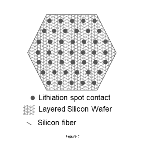
Figure 1 an example of a fuse spot distribution to interconnect
separate lay-
ers of aligned and/or stacked and/or interlaced group IV, in partic-
ular silicon fibres,
Figure 2 an exemplary set up for lithiation of the spot fused layered
silicon
anode body (wafer), patterned solid state (glass)-ceramic electro-
lyte (hexagonal) as-lithiation mask. The lithiation takes place in
steps, e.g., as depicted in figure 2 in four steps, however it is not
limited on this number of steps. Steps can be in between 1-100
steps. lithiation is 1st started preferably in the centre part 1 followed
by the subsequent area to then 3 then 4 and so on.
Figure 3 an abstract image of an over-lithiated silicon anode body,
Figure 4 Patterned solid state (glass)-ceramic electrolyte as-
lithiation mask
resembling the ex-situ lithiation in a process solvent/electrolyte.
Figure 4 depicts the initial state with only limited lithiation and un-
expanded silicon layers which are mechanically interlocked be-
tween each other by the fused spots.
CA 03195681 2023-03-16
WO 2022/179719 - 24 -
PCT/EP2021/075551
Figure 5 Patterned solid state (glass)-ceramic electrolyte as-
lithiation mask
resembling the ex-situ lithiation in a process solvent/electrolyte.
Figure 5 depicts the intermediate state with partly lithiation and ex-
panded silicon layers, which are anisotropically spot fused by lith-
ium induced metallurgic bonds. The arrows mark the lithiation
pathway,
Figure 6 Patterned solid state (glass)-ceramic electrolyte as-
lithiation mask
resembling the ex-situ lithiation in a process solvent/electrolyte.
Figure 6 depicts the complete state with (over)-lithiation and fully
expanded silicon layers, which are anisotropically spot fused by
lithium induced metallurgic bonds. The arrows mark the lithiation
pathway.
Figure 7 Lithiated (5-100%) silicon wafer monolithic body, including ex-
situ fabri-
cated artificial SEI layer,
Figure 8 Graphene and/or reduced graphene oxide current collector foil
in-
cluding 3 tabs,
Figure 9 Lithiated (5-100%) silicon wafer anode monolith, including ex-
situ
fabricated artificial SEI layer attached on top of a graphene and/or
reduced graphene oxide current foil including 3 tabs,
Figure 10-13 show the relative volumetric extent of the layered silicon
anode
(late silicon wafer) in the different non-lithiated, partially lithiated
and over lithiated states. the size of the circles may only represent
the increase in volume but not necessarily the actual percentage
in volume or die me to increase,
Figure 10 Silicon wafer anode in the state of the highest density,
RECTIFIED SHEET (RULE 91) ISA/EP
CA 03195681 2023-03-16
WO 2022/179719 PCT/EP2021/075551
- 25 -
Figure 11 (Electrochemical) lithiated silicon wafer anode in the state
of room tem-
perature active phase Li15Si4.,
Figure 12 (Electrochemical) over-lithiated silicon wafer anode in the
state of the
high temperature active phase Li2iSi5 featuring the maximum possible
volume,
Figure 13 Ex-situ fabricated SEI via the disproportionation of the high
temperature
Li2iSi5 phase to the room temperature phase LimSia. The such released
excess of Li is consumed to build up the artificial SEI layer (red),
Figure 14 a top view on the relative orientation of 3 representative
layers with
aligned silicon fibres each alignment along the direction of the in-
dividual arrows of the same colour Layers of aligned and preferably
1200 interlaced silicon fibers before pre-lithiation process,
Figure 15 the setup of layers according to figure 14 after the pre-
lithiation
(spot fusing) process.