Note: Descriptions are shown in the official language in which they were submitted.
LIGHT SOURCE, SOURCE, MULTIVIEW BACKLIGHT, AND METHOD
WITH A BIFURCATED EMISSION PATTERN
BACKGROUND
[0001] Electronic displays are a nearly ubiquitous medium for
communicating
information to users of a wide variety of devices and products. Most commonly
employed electronic displays include the cathode ray tube (CRT), plasma
display panels
(PDP), liquid crystal displays (LCD), electroluminescent displays (EL),
organic light
emitting diode (OLED) and active matrix OLEDs (AMOLED) displays,
electrophoretic
displays (EP) and various displays that employ electromechanical or
electrofluidic light
modulation (e.g., digital micromirror devices, electrowetting displays, etc.).
Generally,
electronic displays may be categorized as either active displays (i.e.,
displays that emit
light) or passive displays (i.e., displays that modulate light provided by
another source).
Among the most obvious examples of active displays are CRTs, PDPs and
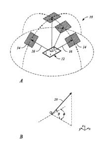
OLEDs/AMOLEDs. Displays that are typically classified as passive when
considering
emitted light are LCDs and EP displays. Passive displays, while often
exhibiting
attractive performance characteristics including, but not limited to,
inherently low power
consumption, may find somewhat limited use in many practical applications
given the
lack of an ability to emit light.
[0002] To overcome the limitations of passive displays associated with
emitted
light, many passive displays are coupled to an external light source. The
coupled light
source may allow these otherwise passive displays to emit light and function
substantially
as an active display. Examples of such coupled light sources are backlights. A
backlight
may serve as a source of light (often a panel backlight) that is placed behind
an otherwise
passive display to illuminate the passive display. For example, a backlight
may be
coupled to an LCD or an EP display. The backlight emits light that passes
through the
LCD or the EP display. The light emitted is modulated by the LCD or the EP
display and
the modulated light is then emitted, in turn, from the LCD or the EP display.
Often
backlights are configured to emit white light. Color filters are then used to
transform the
white light into various colors used in the display. The color filters may be
placed at an
Date Recue/Date Received 2023-04-18
-2-
output of the LCD or the EP display (less common) or between the backlight and
the
LCD or the EP display, for example.
BRIEF DESCRIPTION OF THE DRAWINGS
[0003] Various features of examples and embodiments in accordance with
the
principles described herein may be more readily understood with reference to
the
following detailed description taken in conjunction with the accompanying
drawings,
where like reference numerals designate like structural elements, and in
which:
[0004] Figure 1A illustrates a perspective view of a multiview display
in an
example, according to an embodiment consistent with the principles described
herein.
[0005] Figure 1B illustrates a graphical representation of the angular
components
of a light beam having a particular principal angular direction in an example,
according to
an embodiment consistent with the principles described herein.
[0006] Figure 2 illustrates a cross-sectional view of a diffraction
grating in an
example, according to an embodiment consistent with the principles described
herein.
[0007] Figure 3A illustrates a cross-sectional view of a light source in
an
example, according to an embodiment consistent with the principles described
herein.
[0008] Figure 3B illustrates a magnified cross-sectional view of a
portion of the
light source of Figure 3A in an example, according to an embodiment consistent
with the
principles described herein.
[0009] Figure 4 illustrates a perspective view of an emission control
layer in an
example, according to an embodiment consistent with the principles described
herein.
[0010] Figure 5 illustrates a perspective view of an emission control
layer in an
example, according to an embodiment consistent with the principles described
herein.
[0011] Figure 6A illustrates a cross-sectional view of a groove in a
layer of
transparent material of an emission control layer in an example, according to
an
embodiment consistent with the principles described herein.
[0012] Figure 6B illustrates a cross-sectional view of a groove in a
layer of
transparent material of an emission control layer in an example, according to
another
embodiment consistent with the principles described herein.
Date Recue/Date Received 2023-04-18
-3-
[0013] Figure 6C illustrates a cross-sectional view of a groove in a
layer of
transparent material of an emission control layer in an example, according to
yet another
embodiment consistent with the principles described herein.
[0014] Figure 7A illustrates a cross sectional view of a multiview
backlight in an
example, according to an embodiment consistent with the principles described
herein.
[0015] Figure 7B illustrates a perspective view of a multiview backlight
in an
example, according to an embodiment consistent with the principles described
herein.
[0016] Figure 8 illustrates a block diagram of a multiview backlight in
an
example, according to another embodiment consistent with the principles
described
herein.
[0017] Figure 9 illustrates a flow chart of a method of light source
operation,
according to an embodiment consistent with the principles described herein.
[0018] Certain examples and embodiments have other features that are one
of in
addition to and in lieu of the features illustrated in the above-referenced
figures. These
and other features are detailed below with reference to the above-referenced
figures.
DETAILED DESCRIPTION
[0019] Examples and embodiments in accordance with the principles
described
herein provide a light source having a bifurcated emission pattern and a
multiview
backlight employing the light source, with application to a multiview display.
In
particular, embodiments consistent with the principles described herein
provide a light
source that provides output light having a bifurcated emission pattern, in
various
embodiments. Further, the light source may be used in a multiview backlight
employing
multibeam elements configured to provide or emit directional light beams
having a
plurality of different principal angular directions. In various embodiments,
the directional
light beams emitted by the multiview backlight using the light source having
the
bifurcated emission pattern may have directions corresponding to or consistent
with view
directions of a multiview image or equivalently of a multiview display. The
bifurcated
emission pattern may provide guided light within the multiview backlight that
improves
one or both of an illumination efficiency and an overall brightness of the
multiview
backlight, according to some embodiments.
Date Recue/Date Received 2023-04-18
-4-
[0020] According to various embodiments, the multiview display that
employs
the multiview backlight may be a so-called 'glasses-free' or autostereoscopic
display.
Uses of multiview backlighting in multiview displays described herein include,
but are
not limited to, mobile telephones (e.g., smart phones), watches, tablet
computes, mobile
computers (e.g., laptop computers), personal computers and computer monitors,
automobile display consoles, camera displays, and various other mobile as well
as
substantially non-mobile display applications and devices.
[0021] Herein a 'two-dimensional (2D) display' is defined as a display
configured
to provide a view of an image that is substantially the same regardless of a
direction from
which the image is viewed (i.e., within a predefined viewing angle or range of
the 2D
display). A liquid crystal display (LCD) found in many smart phones and
computer
monitors are examples of 2D displays. In contrast herein, a `multiview
display' is
defined as an electronic display or display system configured to provide
different views
of a multiview image in or from different view directions. In particular, the
different
views may represent different perspective views of a scene or object of the
multiview
image. In some instances, a multiview display may also be referred to as a
three-
dimensional (3D) display, e.g., when simultaneously viewing two different
views of the
multiview image provides a perception of viewing a three-dimensional image.
[0022] Figure 1A illustrates a perspective view of a multiview display
10 in an
example, according to an embodiment consistent with the principles described
herein. As
illustrated in Figure 1A, the multiview display 10 comprises a screen 12 to
display a
multiview image to be viewed. The multiview display 10 provides different
views 14 of
the multiview image in different view directions 16 relative to the screen 12.
The view
directions 16 are illustrated as arrows extending from the screen 12 in
various different
principal angular directions; the different views 14 are illustrated as shaded
polygonal
boxes at the termination of the arrows (i.e., depicting the view directions
16); and only
four views 14 and four view directions 16 are illustrated, all by way of
example and not
limitation. Note that while the different views 14 are illustrated in Figure
1A as being
above the screen, the views 14 actually appear on or in a vicinity of the
screen 12 when
the multiview image is displayed on the multiview display 10. Depicting the
views 14
above the screen 12 is only for simplicity of illustration and is meant to
represent viewing
Date Recue/Date Received 2023-04-18
-5-
the multiview display 10 from a respective one of the view directions 16
corresponding to
a particular view 14.
[0023] A view direction or equivalently a light beam having a direction
corresponding to a view direction of a multiview display generally has a
principal angular
direction given by angular components {0, 0}, by definition herein. The
angular
component 0 is referred to herein as the 'elevation component' or 'elevation
angle' of the
light beam. The angular component 0 is referred to as the 'azimuth component'
or
'azimuth angle' of the light beam. By definition, the elevation angle 0 is an
angle in a
vertical plane (e.g., perpendicular to a plane of the multiview display screen
while the
azimuth angle 0 is an angle in a horizontal plane (e.g., parallel to the
multiview display
screen plane).
[0024] Figure 1B illustrates a graphical representation of the angular
components
{0, 0} of a light beam 20 having a particular principal angular direction or
simply
'direction' corresponding to a view direction (e.g., view direction 16 in
Figure 1A) of a
multiview display in an example, according to an embodiment consistent with
the
principles described herein. In addition, the light beam 20 is emitted or
emanates from a
particular point, by definition herein. That is, by definition, the light beam
20 has a
central ray associated with a particular point of origin within the multiview
display.
Figure 1B also illustrates the light beam (or view direction) point of origin,
0.
[0025] Further herein, the term `multiview' as used in the terms
`multiview
image' and `multiview display' is defined as a plurality of views representing
different
perspectives or including angular disparity between views of the view
plurality. In
addition, herein the term `multiview' explicitly includes more than two
different views
(i.e., a minimum of three views and generally more than three views), by
definition
herein. As such, `multiview display' as employed herein is explicitly
distinguished from
a stereoscopic display that includes only two different views to represent a
scene or an
image. Note however, while multiview images and multiview displays may include
more
than two views, by definition herein, multiview images may be viewed (e.g., on
a
multiview display) as a stereoscopic pair of images by selecting only two of
the
multiview views to view at a time (e.g., one view per eye).
Date Recue/Date Received 2023-04-18
-6-
[0026] A `multiview pixel' is defined herein as a set of sub-pixels or
'view' pixels
in each of a similar plurality of different views of a multiview display. In
particular, a
multiview pixel may have individual view pixels corresponding to or
representing a view
pixel in each of the different views of the multiview image. Moreover, the
view pixels of
the multiview pixel are so-called 'directional pixels' in that each of the
view pixels is
associated with a predetermined view direction of a corresponding one of the
different
views, by definition herein. Further, according to various examples and
embodiments,
the different view pixels of a multiview pixel may have equivalent or at least
substantially
similar locations or coordinates in each of the different views. For example,
a first
multiview pixel may have individual view pixels located at {xiyi } in each of
the different
views of a multiview image, while a second multiview pixel may have individual
view
pixels located at {x2y2 } in each of the different views, and so on. In some
embodiments,
a number of view pixels in a multiview pixel may be equal to a number of views
of the
multiview display.
[0027] Herein, a 'light guide' is defined as a structure that guides
light within the
structure using total internal reflection or `TIR'. In particular, the light
guide may include
a core that is substantially transparent at an operational wavelength of the
light guide. In
various examples, the term 'light guide' generally refers to a dielectric
optical waveguide
that employs total internal reflection to guide light at an interface between
a dielectric
material of the light guide and a material or medium that surrounds that light
guide. By
definition, a condition for total internal reflection is that a refractive
index of the light
guide is greater than a refractive index of a surrounding medium adjacent to a
surface of
the light guide material. In some embodiments, the light guide may include a
coating in
addition to or instead of the aforementioned refractive index difference to
further
facilitate the total internal reflection. The coating may be a reflective
coating, for
example. The light guide may be any of several light guides including, but not
limited to,
one or both of a plate or slab guide and a strip guide.
[0028] Further herein, the term 'plate' when applied to a light guide as
in a 'plate
light guide' is defined as a piecewise or differentially planar layer or
sheet, which is
sometimes referred to as a 'slab' guide. In particular, a plate light guide is
defined as a
light guide configured to guide light in two substantially orthogonal
directions bounded
Date Recue/Date Received 2023-04-18
-7-
by a top surface and a bottom surface (i.e., opposite surfaces) of the light
guide. Further,
by definition herein, the top and bottom surfaces are both separated from one
another and
may be substantially parallel to one another in at least a differential sense.
That is, within
any differentially small section of the plate light guide, the top and bottom
surfaces are
substantially parallel or co-planar.
[0029] In some embodiments, the plate light guide may be substantially
flat (i.e.,
confined to a plane) and therefore, the plate light guide is a planar light
guide. In other
embodiments, the plate light guide may be curved in one or two orthogonal
dimensions.
For example, the plate light guide may be curved in a single dimension to form
a
cylindrical shaped plate light guide. However, any curvature has a radius of
curvature
sufficiently large to ensure that total internal reflection is maintained
within the plate light
guide to guide light.
[0030] As defined herein, a 'non-zero propagation angle' of guided light
is an
angle relative to a guiding surface of a light guide. Further, the non-zero
propagation
angle is both greater than zero and less than a critical angle of total
internal reflection
within the light guide, by definition herein. Moreover, a specific non-zero
propagation
angle may be chosen (e.g., arbitrarily) for a particular implementation as
long as the
specific non-zero propagation angle is less than the critical angle of total
internal
reflection within the light guide. In various embodiments, the light may be
introduced or
coupled into the light guide at the non-zero propagation angle of the guided
light.
[0031] According to various embodiments, guided light or equivalently a
guided
'light beam' produced by coupling light into the light guide may be a
collimated light
beam. Herein, a 'collimated light' or 'collimated light beam' is generally
defined as a
beam of light in which rays of the light beam are substantially parallel to
one another
within the light beam. Further, rays of light that diverge or are scattered
from the
collimated light beam are not considered to be part of the collimated light
beam, by
definition herein.
[0032] Herein, a 'diffraction grating' is generally defined as a
plurality of features
(i.e., diffractive features) arranged to provide diffraction of light incident
on the
diffraction grating. In some examples, the plurality of features may be
arranged in a
periodic or quasi-periodic manner. For example, the diffraction grating may
include a
Date Recue/Date Received 2023-04-18
-8-
plurality of features (e.g., a plurality of grooves or ridges in a material
surface) arranged
in a one-dimensional (1D) array. In other examples, the diffraction grating
may be a two-
dimensional (2D) array of features. The diffraction grating may be a 2D array
of bumps
on or holes in a material surface, for example.
[0033] As such, and by definition herein, the 'diffraction grating' is a
structure
that provides diffraction of light incident on the diffraction grating. If the
light is incident
on the diffraction grating from a light guide, the provided diffraction or
diffractive
scattering may result in, and thus be referred to as, 'diffractive scattering'
in that the
diffraction grating may scatter light out of the light guide by diffraction.
Further, by
definition herein, the features of a diffraction grating are referred to as
'diffractive
features' and may be one or more of at, in, and on a material surface (i.e., a
boundary
between two materials). The surface may be a surface of a light guide, for
example. The
diffractive features may include any of a variety of structures that diffract
light including,
but not limited to, one or more of grooves, ridges, holes and bumps at, in or
on the
surface. For example, the diffraction grating may include a plurality of
substantially
parallel grooves in the material surface. In another example, the diffraction
grating may
include a plurality of parallel ridges rising out of the material surface. The
diffractive
features (e.g., grooves, ridges, holes, bumps, etc.) may have any of a variety
of cross-
sectional shapes or profiles that provide diffraction including, but not
limited to, one or
more of a sinusoidal profile, a rectangular profile (e.g., a binary
diffraction grating), a
triangular profile and a saw tooth profile (e.g., a blazed grating).
[0034] According to various examples described herein, a diffraction
grating (e.g.,
a diffraction grating of a multibeam element, as described below) may be
employed to
diffractively scatter or couple light out of a light guide (e.g., a plate
light guide) as a light
beam. In particular, a diffraction angle Om of or provided by a locally
periodic diffraction
grating may be given by equation (1) as:
Om = sin-1 (n sin Oi ¨ (1)
where A is a wavelength of the light, m is a diffraction order, n is an index
of refraction of
a light guide, d is a distance or spacing between features of the diffraction
grating, Oi is an
angle of incidence of light on the diffraction grating. For simplicity,
equation (1)
Date Recue/Date Received 2023-04-18
-9-
assumes that the diffraction grating is adjacent to a surface of the light
guide and a
refractive index of a material outside of the light guide is equal to one
(i.e., 71.0õt = 1). In
general, the diffraction order m is given by an integer. A diffraction angle
Om of a light
beam produced by the diffraction grating may be given by equation (1) where
the
diffraction order is positive (e.g., m > 0). For example, first-order
diffraction is provided
when the diffraction order m is equal to one (i.e., m = 1).
[0035] Figure 2 illustrates a cross-sectional view of a diffraction
grating 30 in an
example, according to an embodiment consistent with the principles described
herein.
For example, the diffraction grating 30 may be located on a surface of a light
guide 40.
In addition, Figure 2 illustrates a light beam 50 incident on the diffraction
grating 30 at an
incident angle O. The incident light beam 50 may be a beam of guided light
(i.e., a
guided light beam) within the light guide 40. Also illustrated in Figure 2 is
a directional
light beam 60 diffractively produced and coupled-out by the diffraction
grating 30 as a
result of diffraction of the incident light beam 50. The directional light
beam 60 has a
diffraction angle Om (or 'principal angular direction' herein) as given by
equation (1).
The diffraction angle Om may correspond to a diffraction order `m' of the
diffraction
grating 30, for example diffraction order m = 1 (i.e., a first diffraction
order).
[0036] By definition herein, a `multibeam element' is a structure or
element of a
backlight or a display that produces light that includes a plurality of light
beams. In some
embodiments, the multibeam element may be optically coupled to a light guide
of a
backlight to provide the plurality of light beams by coupling or scattering
out a portion of
light guided in the light guide. Further, the light beams of the plurality of
light beams
produced by a multibeam element have different principal angular directions
from one
another, by definition herein. In particular, by definition, a light beam of
the plurality has
a predetermined principal angular direction that is different from another
light beam of
the light beam plurality. As such, the light beam is referred to as a
'directional light
beam' and the light beam plurality may be termed a 'directional light beam
plurality,' by
definition herein.
[0037] Furthermore, the directional light beam plurality may represent a
light
field. For example, the directional light beam plurality may be confined to a
substantially
conical region of space or have a predetermined angular spread that includes
the different
Date Recue/Date Received 2023-04-18
-to-
principal angular directions of the light beams in the light beam plurality.
As such, the
predetermined angular spread of the light beams in combination (i.e., the
light beam
plurality) may represent the light field.
[0038] According to various embodiments, the different principal angular
directions of the various directional light beams of the plurality are
determined by a
characteristic including, but not limited to, a size (e.g., length, width,
area, etc.) of the
multibeam element. In some embodiments, the multibeam element may be
considered an
'extended point light source', i.e., a plurality of point light sources
distributed across an
extent of the multibeam element, by definition herein. Further, a directional
light beam
produced by the multibeam element has a principal angular direction given by
angular
components {0, 0}, by definition herein, and described above with respect to
Figure 1B.
[0039] Herein a 'collimator' is defined as substantially any optical
device or
apparatus that is configured to collimate light. For example, a collimator may
include,
but is not limited to, a collimating mirror or reflector, a collimating lens,
a diffraction
grating, a tapered light guide, and various combinations thereof. According to
various
embodiments, an amount of collimation provided by the collimator may vary in a
predetermined degree or amount from one embodiment to another. Further, the
collimator may be configured to provide collimation in one or both of two
orthogonal
directions (e.g., a vertical direction and a horizontal direction). That is,
the collimator
may include a shape or similar collimating characteristic in one or both of
two orthogonal
directions that provides light collimation, according to some embodiments.
[0040] Herein, a 'collimation factor' is defined as a degree to which
light is
collimated. In particular, a collimation factor defines an angular spread of
light rays
within a collimated beam of light, by definition herein. For example, a
collimation factor
a may specify that a majority of light rays in a beam of collimated light is
within a
particular angular spread (e.g., +1- a degrees about a central or principal
angular direction
of the collimated light beam). The light rays of the collimated light beam may
have a
Gaussian distribution in terms of angle and the angular spread may be an angle
determined by at one-half of a peak intensity of the collimated light beam,
according to
some examples.
Date Recue/Date Received 2023-04-18
-11-
[0041] Herein, a 'light source' is generally defined as a source of
light (e.g., an
optical emitter configured to produce and emit light). For example, the light
source may
comprise an optical emitter such as a light emitting diode (LED) that emits
light when
activated or turned on. In particular, herein the light source may be
substantially any
source of light or comprise substantially any optical emitter including, but
not limited to,
one or more of a light emitting diode (LED), a laser, an organic light
emitting diode
(OLED), a polymer light emitting diode, a plasma-based optical emitter, a
fluorescent
lamp, an incandescent lamp, and virtually any other source of light. The light
produced
by the light source may have a color (i.e., may include a particular
wavelength of light),
or may be a range of wavelengths (e.g., white light). In some embodiments, the
light
source may comprise a plurality of optical emitters. For example, the light
source may
include a set or group of optical emitters in which at least one of the
optical emitters
produces light having a color, or equivalently a wavelength, that differs from
a color or
wavelength of light produced by at least one other optical emitter of the set
or group. The
different colors may include primary colors (e.g., red, green, blue) for
example. In
another example, plurality of optical emitters may be arranged in a row or as
array across
a width of the light source.
[0042] Further, as used herein, the article 'a' is intended to have its
ordinary
meaning in the patent arts, namely 'one or more'. For example, 'a multibeam
element'
means one or more multibeam elements and as such, 'the multibeam element'
means 'the
multibeam element(s)' herein. Also, any reference herein to 'top', 'bottom',
'upper',
'lower', 'up', 'down', 'front', back', 'first', 'second', 'left' or 'right' is
not intended to be
a limitation herein. Herein, the term 'about' when applied to a value
generally means
within the tolerance range of the equipment used to produce the value, or may
mean plus
or minus 10%, or plus or minus 5%, or plus or minus 1%, unless otherwise
expressly
specified. Further, the term 'substantially' as used herein means a majority,
or almost all,
or all, or an amount within a range of about 51% to about 100%. Moreover,
examples
herein are intended to be illustrative only and are presented for discussion
purposes and
not by way of limitation.
[0043] In accordance with principles disclosed herein, a light source is
provided.
Figure 3A illustrates a cross-sectional view of a light source 100 in an
example, according
Date Recue/Date Received 2023-04-18
-12-
to an embodiment consistent with the principles described herein. Figure 3B
illustrates a
magnified cross-sectional view of a portion of the light source 100 of Figure
3A in an
example, according to an embodiment consistent with the principles described
herein. In
particular, Figures 3A and 3B depict an embodiment of the light sources 100
useful, for
example, in a multiview backlight, as describe in more detail below with
reference to
Figures 7A and 7B.
[0044] According to various embodiments, the light source 100 comprises
an
optical emitter 110. In some embodiments, the optical emitter 110 may be or
comprise
any of a variety of optical emitters including, but not limited to, a light
emitting diode
(LED) or a laser (e.g., a laser diode). In some embodiments, the optical
emitter 110 may
comprise a plurality or an array of optical emitters (e.g., a LED array)
distributed in a
horizontal direction (y-direction) or across a width of the light source 100.
The optical
emitter 110 is configured to emit light as emitted light 112. In various
embodiments, the
emitted light 112 may be directed by the optical emitter 110 in a general
direction toward
an output aperture 102 of the light source 100. In this connection and when
the optical
emitter 110 comprises an LED, the light source 100 may be referred to as an
LED
package. Further, the optical emitter 110 may provide the emitted light 112 in
a relatively
uncollimated form or as a beam of light having a relatively broad beamwidth
(e.g., greater
than about ninety degrees), in some embodiments. In particular, an emission
pattern of
the emitted light 112 may have a Lambertian distribution, i.e., a single lobe
as illustrated
in Figure 3A, in some embodiments.
[0045] As illustrated, the light source 100 further comprises an
emission control
layer 120. According to various embodiments (e.g., as illustrated), the
emission control
layer 120 comprises a first plurality of light-blocking elements 122 and a
second plurality
of light-blocking elements 124. As illustrated, the first plurality of light-
blocking
elements 122 or light-blocking elements 122 of the first plurality are spaced
apart from
one another in a vertical direction at the output aperture 102, e.g., along a
z-axis.
According to various embodiments, the second plurality of light-blocking
elements 124
or light-blocking elements of the second plurality are displaced from the
output aperture
102 and interleaved with the first plurality of light-blocking elements 122.
For example,
the second plurality of light-blocking elements 124 is illustrated in Figures
3A-3B as
Date Recue/Date Received 2023-04-18
-13-
being displaced toward the optical emitter 110 along an x-axis. Further, as
illustrated,
individual light-blocking element 124 of the second plurality are interleaved
between
individual light-blocking elements 122 of the first plurality. As such, when
considered in
an x-direction in Figure 3A, the individual light-blocking elements 124 are
aligned with
spaces between the individual light-blocking elements 122, i.e., the second
plurality of
light-blocking elements 124 is interleaved with the first plurality of light-
blocking
elements 122 along the z-direction when considered from the x-direction, as
illustrated.
[0046] According to various embodiments, the emission control layer is
configured to transmit a portion of the emitted light 112 through gaps 120a,
120b between
light-blocking elements 122, 124 of the first plurality of light-blocking
elements 122 and
the second plurality of light-blocking elements 124. Transmission of the
emitted light
portion is configured to provide output light 104 having a bifurcated emission
pattern in
the vertical direction, e.g., z-direction, at the output aperture 102 of the
light source 100
as illustrated. In particular, the bifurcated emission pattern of the output
light may
comprise a first lobe 104a having a positive angle in the vertical direction
(z-direction)
and a second lobe 104b having a negative angle in the vertical direction (z-
direction),
according to some embodiments. The first lobe 104a of the bifurcated emission
pattern of
the output light 104 may comprise a portion of the emitted light 112
transmitted through a
set of first gaps 120a, while a set of second gaps 120b through which another
portion of
the emitted light 112 is transmitted may provide output light 104 of the
second lobe 104b,
for example. Further, the positive and negative angles of the first and second
lobes 104a,
104b of the bifurcated emission pattern may be angles defined in an x-z plane
relative to a
surface normal of the output aperture 102, i.e., the x-axis as illustrated in
Figure 3A.
[0047] According to various embodiments, the light-blocking elements
122, 124
may comprise virtually any opaque material that blocks or at least
substantially block
transmission of light. For example, the light-blocking elements 122, 124 may
comprise a
black paint or black ink. In another example, light-blocking elements 122, 124
may
comprise an opaque transparent material, layer, or strip. In some embodiments,
the light-
blocking elements 122, 124 may comprise a reflective material. In particular,
the light-
blocking elements 122, 124 may comprise one or more of a one of a reflective
metal (e.g.,
aluminum, gold, silver, copper, nickel, etc.) and a reflective metal-polymer
composite
Date Recue/Date Received 2023-04-18
-14-
(e.g., an aluminum-polymer composite). In some embodiments, the light-blocking
elements 122, 124 may comprise the same material (e.g., may both be a
reflective metal
or reflective metal-polymer composite). In other embodiments, materials and
material
characteristics of the light-blocking elements 122 of the first plurality may
differ from
materials and material characteristics of the light-blocking elements 124 of
the second
plurality. For example, the first plurality of light-blocking elements 122 may
comprise a
reflective material and the second plurality of light-blocking elements 124
may comprise
an opaque, but substantially non-reflective, material.
[0048] In some embodiments, the light-blocking elements 122, 124 of the
first
and second pluralities are or comprise strips of a material (e.g., an opaque
material, a
reflective material, etc.). Figure 4 illustrates a perspective view of an
emission control
layer 120 in an example, according to an embodiment consistent with the
principles
described herein. As illustrated in Figure 4, the first plurality of light-
blocking elements
122 comprises strips of opaque material spaced apart from one another in the z-
direction,
e.g., in a plane of the output aperture 102. The second plurality of light-
blocking
elements 124 illustrated in Figure 4 is displaced from the plane of the first
plurality in the
x-direction. Further, light-blocking elements 124 of the second plurality also
comprise
strips of opaque material that are spaced apart from one another in the z-
direction to
interleave with the first plurality of light-blocking elements 122. Also
illustrated in
Figure 4 are the first and second gaps 120a, 120b between the light-blocking
elements
122,124 of the first plurality of light-blocking elements 122 and the second
plurality of
light-blocking elements 124.
[0049] According to some embodiments, emission control layer may further
comprise sheet or layer of transparent material between the optical emitter
and the output
aperture, the transparent material layer having a plurality of grooves
oriented in a
horizontal direction in a surface of the transparent material layer adjacent
to the output
aperture. Figure 5 illustrates a perspective view of an emission control layer
120 in an
example, according to an embodiment consistent with the principles described
herein. In
particular, Figure 5 illustrates an emission control layer 120 comprising a
layer of
transparent material 126 having grooves 128 oriented in a horizontal direction
(y-
direction) in a surface of the transparent material 126. According to these
embodiments,
Date Recue/Date Received 2023-04-18
-15-
the light-blocking elements 122 of the first plurality of light-blocking
elements 122 may
comprise a layer of light-blocking material disposed on transparent material
layer surface
between grooves 128 of the groove plurality, e.g., as illustrated. Further, as
illustrated,
the light-blocking elements 124 of the second plurality of light-blocking
elements 124
may comprise a layer of light-blocking material disposed on or at a bottom of
each of the
grooves 128 of the groove plurality, according to some of these embodiments.
For
example, a layer of reflective material (e.g., reflective metal or reflective
metal-polymer
composite) may be provided or deposited (e.g., by sputter deposition,
evaporative
deposition, printing, etc.) on the bottoms of the grooves 128 and on the
surface of the
layer of transparent material 126 between the grooves 128 to provide the light-
blocking
elements 122, 124. According to various embodiments, the transparent material
126 of
the transparent material layer may comprise virtually any optically
transparent or
substantially transparent material including, but not limited to, one or more
of various
types of glass (e.g., silica glass, alkali-aluminosilicate glass, borosilicate
glass, etc.),
substantially optically transparent plastics or polymers (e.g., poly(methyl
methacrylate) or
'acrylic glass', polycarbonate, etc.), and similar other dielectric materials.
[0050] According to various embodiments, the grooves 128 may have side
walls
with various shapes and configurations. For example, a side wall of a groove
128 of the
groove plurality may be perpendicular or substantially perpendicular to the
transparent
material layer surface. In another example, a side wall of a groove 128 of the
groove
plurality may comprises a curved shape. A slope of the side wall may be either
positive
or negative and each side wall of the groove 128 may have either the same
shape or
different shapes from one another, according to various embodiments.
[0051] Figure 6A illustrates a cross-sectional view of a groove 128 in a
layer of
transparent material 126 of an emission control layer 120 in an example,
according to an
embodiment consistent with the principles described herein. In particular,
Figure 6A
illustrates the groove 128 having perpendicular side walls 128a. Also
illustrated in Figure
6A are light-blocking elements 122 of the first plurality of light-blocking
elements 122 on
the transparent material surface between grooves 128 of the groove plurality
and light-
blocking elements 124 of the second plurality of light-blocking elements 124
on or at the
bottoms of the grooves 128. A width of the light-blocking elements 122, 124
respectively
Date Recue/Date Received 2023-04-18
-16-
of the first plurality and the second plurality may be substantially similar
by virtue of the
perpendicular side walls 128a, for example as illustrated in Figure 6A.
[0052] Figure 6B illustrates a cross-sectional view of a groove 128 in a
layer of
transparent material 126 of the emission control layer 120 in an example,
according to
another embodiment consistent with the principles described herein. As
illustrated in
Figure 6B, the groove 128 has curved side walls 128b. Figure 6B also
illustrates light-
blocking elements 122 of the first plurality on the surface of the transparent
material
between grooves 128 of the groove plurality and light-blocking elements 124 of
the
second plurality on or at the bottoms of the grooves 128.
[0053] Figure 6C illustrates a cross-sectional view of a groove 128 in a
layer of
transparent material 126 of the emission control layer 120 in an example,
according to yet
another embodiment consistent with the principles described herein. In
particular, Figure
6C illustrates the groove 128 having sloped side walls 128c. The sloped side
walls 128c
illustrated in Figure 6C have a negative slope, as illustrated by way of
example and not
limitation. By virtue of the negative slope, the light-blocking elements 124
of the second
plurality at the bottom of the grooves 128 are wider than the light-blocking
elements 122
of the first plurality, as illustrated in Figure 6C. Note that, if the sloped
side walls 128c
were to have a positive slope (not illustrated), the light-blocking elements
124 of the
second plurality of light-blocking elements 124 would be generally narrower
than the
light-blocking elements 122 of the first plurality.
[0054] In some embodiments (not illustrated), for example when the light-
blocking elements 122, 124 of one or both of the first plurality of light-
blocking elements
122 and the second plurality of light-blocking elements 124 comprises a
reflective
material, the emission control layer 120 may be configured recycle light
reflected by the
light-blocking elements 122, 124. In particular, the light-blocking elements
122, 124 may
be configured to reflect a portion of the emitted light 112 away from the
output aperture
102 and toward the optical emitter 110. The reflected portion may be recycled
and
redirected toward the emission control layer 120 by the optical emitter 110,
according to
some embodiments. For example, the optical emitter 110 may comprise a
reflector or a
reflective scattering layer that redirects the reflected portion back toward
the output
aperture 102. The reflector may be part of a housing of the optical emitter
110, for
Date Recue/Date Received 2023-04-18
-17-
example. In another example, the emission control layer 120 may comprise the
reflector
or partially reflective layer, e.g., at an input surface of the emission
control layer 120, that
is configured to selectively reflect and redirect the reflected portion back
toward the
output aperture 102 of the light source 100. Examples of partially reflective
layers
include, but are not limited to, a reflective polarizer and a so-called half-
silvered mirror.
Recycling the reflected portion may yield improved brightness or increased
power
efficiency of the light source 100, according to various embodiments.
[0055] In some embodiments, one or more of a size or width of the light-
blocking
elements 122, 124, a displacement or separation between the first plurality of
light-
blocking elements 122 and the second plurality of light-blocking elements 124,
and a
number of light-blocking elements 122, 124 in the first plurality and the
second plurality
may be chosen to control characteristics of the bifurcated emission pattern.
For example,
by selecting or changing the displacement or separation, an angle of the first
and second
lobes 104a, 104b of the bifurcated emission pattern may be adjusted. In
another example,
a spread angle of the first and second lobes 104a, 104b may be determined by a
width of
the light-blocking elements 122, 124.
[0056] In some embodiments, the width of the light-blocking elements
122, 124
of the first plurality and the second plurality may be between about five
micrometers gm
(5 gm) and about fifty micrometers (50 gm). For example, the width of each of
the light-
blocking elements 122, 124 may be about twenty-five micrometers (25 gm). In
other
examples, the width of the light-blocking elements 122, 124 may be between
about ten
micrometers (10 gm) and about forty micrometers (40 gm) or between about
twenty
micrometers (20 gm) and about thirty micrometers (30 gm). In some embodiments,
the
displacement or separation between the first plurality of light-blocking
elements 122 and
the second plurality of light-blocking elements 124 may be between about five
micrometers (5 gm) and about fifty micrometers (50 gm). For example, the
displacement
between the first plurality of light-blocking elements 122 and the second
plurality may be
about twenty-five micrometers (25 gm). In other examples, the displacement may
be
between about ten micrometers (10 gm) and about forty micrometers (40 gm) or
between
about twenty micrometers (20 gm) and about thirty micrometers (30 gm). In some
embodiments, there may be between about three (3) and about fifty (50) light-
blocking
Date Recue/Date Received 2023-04-18
-18-
elements 122 in the first plurality or between about two (2) and about forty-
nine (49)
light-blocking elements 124 in the second plurality. For example, there may be
about
eight (8) light-blocking elements 122 in the first plurality and about seven
(7) light-
blocking elements 124 in the second plurality. In some embodiments, light-
blocking
elements 122, 124 in each of the first plurality and second plurality have
equal widths,
e.g., a duty cycle of fifty percent (50%). In other embodiments, a width of
the light-
blocking elements 122 of the first plurality may differ from a width of the
light-blocking
elements 124 of the second plurality. In these embodiments, the duty cycle of
the light-
blocking element widths may range between about one percent (1%) and about
seventy-
five percent (75%). Note that the width of light-blocking elements 122 of the
first
plurality may be either greater than or less than the width of the light-
blocking elements
124 of the second plurality when the duty cycle is not fifty percent (50%),
i.e., the duty
cycle may be positive or negative in some embodiments. Further, the above
width
dimensions are based on a light guide thickness of about four hundred
micrometers (400
m) and may be adjusted accordingly for other light guide thicknesses, e.g.,
the light
guide 210 described below.
[0057] In some embodiments, the light source 100 may be used to provide
light to
backlight such as, but not limited to, a multiview backlight. In particular,
according to
some embodiments of the principles described herein, a multiview backlight
comprising a
light source substantially similar to the light source 100 described above is
provided.
[0058] Figure 7A illustrates a cross sectional view of a multiview
backlight 200 in
an example, according to an embodiment consistent with the principles
described herein.
Figure 7B illustrates a perspective view of a multiview backlight 200 in an
example,
according to an embodiment consistent with the principles described herein.
The
multiview backlight 200 illustrated in Figures 7A and 7B is configured to
provide
directional light beams 202 having different principal angular directions from
one another
(e.g., as a light field). In particular, the provided directional light beams
202 are directed
away from the multiview backlight 200 in different principal angular
directions
corresponding to respective view directions of a multiview display, according
to various
embodiments. In some embodiments, the directional light beams 202 may be
modulated
Date Recue/Date Received 2023-04-18
-19-
(e.g., using light valves, as described below) to facilitate the display of
information
having 3D content.
[0059] As illustrated in Figures 7A-7B, the multiview backlight 200
comprises a
light guide 210. The light guide 210 may be a plate light guide, according to
some
embodiments. The light guide 210 is configured to guide light along a length
of the light
guide 210 as guided light 204. For example, the light guide 210 may include a
dielectric
material configured as an optical waveguide. The dielectric material may have
a first
refractive index that is greater than a second refractive index of a medium
surrounding
the dielectric optical waveguide. The difference in refractive indices is
configured to
facilitate total internal reflection of the guided light 204 according to one
or more guided
modes of the light guide 210, for example.
[0060] In some embodiments, the light guide 210 may be a slab or plate
optical
waveguide comprising an extended, substantially planar sheet of optically
transparent,
dielectric material. The substantially planar sheet of dielectric material is
configured to
guide the guided light 204 using total internal reflection. According to
various examples,
the optically transparent material of the light guide 210 may include or be
made up of any
of a variety of dielectric materials including, but not limited to, one or
more of various
types of glass (e.g., silica glass, alkali-aluminosilicate glass, borosilicate
glass, etc.) and
substantially optically transparent plastics or polymers (e.g., poly(methyl
methacrylate) or
'acrylic glass', polycarbonate, etc.). In some examples, the light guide 210
may further
include a cladding layer (not illustrated) on at least a portion of a surface
(e.g., one or
both of the top surface and the bottom surface) of the light guide 210. The
cladding layer
may be used to further facilitate total internal reflection, according to some
examples.
According to various embodiments, the light guide 210 is configured to guide
the guided
light 204 according to total internal reflection at a non-zero propagation
angle between a
first guiding surface 210' (e.g., 'front' surface or side) and a second
guiding surface 210"
(e.g., 'back' surface or side) of the light guide 210. The guided light 204
may also be
guided according to a collimation factor a, according to some embodiments. As
defined
herein, a 'non-zero propagation angle' is an angle relative to a guiding
surface (e.g., the
first guiding surface 210' or the second guiding surface 210") of the light
guide 210.
Further, the non-zero propagation angle is both greater than zero and less
than a critical
Date Recue/Date Received 2023-04-18
-20-
angle of total internal reflection within the light guide 210, according to
various
embodiments. In Figure 7A, a bold arrow indicating a propagation direction 203
of the
guided light (e.g., directed in the x-direction) of the guided light 204
within the light
guide 210.
[0061] As illustrated in Figures 7A-7B, the multiview backlight 200
further
comprises a light source 220 configured to provide output light having a
bifurcated
emission pattern to be guided within the light guide 210 as the guided light
204. As
illustrated, the light source 220 is optically coupled to an input edge of the
light guide 210
and is configured to introduce the output light having the bifurcated emission
pattern into
the light guide 210 through the input edge. Once introduced and guided by the
light
guide 210, the output light becomes or serves as the guided light 204, which
also has or
includes a bifurcated emission pattern. In particular, the bifurcated emission
pattern
comprises a first lobe 204a having an angle toward the first guiding surface
210' of the
light guide 210 and a second lobe 204b having angle toward the second guiding
surface
210" of the light guide 210, as illustrated. Angles of the first and second
lobes 204a,
204b may correspond to the non-zero propagation angles of the guided light
204,
according to various embodiments.
[0062] According to some embodiments, the light source 220 may be
substantially similar to the light source 100, described above. For example,
as illustrated
in Figure 7A, the light source 220 comprises an optical emitter 222 and an
emission
control layer 224. In some embodiments, the optical emitter 222 may be
substantially
similar to the optical emitter 110 of the above-described light source 100.
Similarly, the
emission control layer 224 may be substantially similar to the emission
control layer 120
described above with respect to the light source 100, according to some
embodiments. In
particular, the emission control layer 224 comprises a first plurality of
light-blocking
elements and a second plurality of light-blocking elements, the second
plurality being
displaced away from and interleaved with the first plurality, as illustrated.
The emission
control layer 224 converts light emitted by the optical emitter 222 into
output light having
the bifurcated emission pattern by transmitting light through gaps between the
light-
blocking elements of the first and second pluralities, respectively.
Date Recue/Date Received 2023-04-18
-21-
[0063] According to various embodiments (e.g., as illustrated in Figures
7A-7B),
the multiview backlight 200 further comprises an array of multibeam elements
230
spaced apart from one another along a length of or generally across the light
guide 210.
In particular, the multibeam elements 230 of the multibeam element array are
separated
from one another by a finite space and represent individual, distinct elements
along the
light guide length.
[0064] According to some embodiments, the multibeam elements 230 of the
array
may be arranged in either a one-dimensional (1D) array or two-dimensional (2D)
array.
For example, the plurality of multibeam elements 230 may be arranged as a
linear 1D
array. In another example, the array of multibeam elements 230 may be arranged
as a
rectangular 2D array or even as a circular 2D array. Further, the array (i.e.,
1D or 2D
array) may be a regular or uniform array, in some examples. In particular, an
inter-
element distance (e.g., center-to-center distance or spacing) between the
multibeam
elements 230 may be substantially uniform or constant across the array. In
other
examples, the inter-element distance between the multibeam elements 230 may be
varied
one or both of across the array and along the length of the light guide 210.
[0065] According to various embodiments, each multibeam element 230 of
the
multibeam element array is configured to couple or scatter out a portion of
the guided
light 204 as the directional light beams 202. In particular, Figures 7A-7B
illustrate the
directional light beams 202 as a plurality of diverging arrows depicted as
being directed
way from the first (or front) guiding surface 210' of the light guide 210.
According to
some embodiments (e.g., as illustrated in Figure 7A), multibeam elements 230
of the
multibeam element array may be located at the first guiding surface 210' of
the light
guide 210. In other embodiments (not illustrated), the multibeam elements 230
may be
located within the light guide 210. In yet other embodiments (not
illustrated), the
multibeam elements 230 may be located at or on the second guiding surface 210"
of the
light guide 210. Further, a size of the multibeam element 230 may be
comparable to a
size of a light valve of a multiview display that employs the multiview
backlight 200.
[0066] Figures 7A and 7B also illustrate an array of light valves 206
(e.g., of the
multiview display), by way of example and not limitation. In various
embodiments, any
of a variety of different types of light valves may be employed as the light
valves 206 of
Date Recue/Date Received 2023-04-18
-22-
the light valve array including, but not limited to, one or more of liquid
crystal light
valves, electrophoretic light valves, and light valves based on or employing
electrowetting. Further, as illustrated, there may be one unique set of light
valves 206 for
each multibeam element 230 of the array of multibeam elements 230. The light
valve
array may be configured to modulate the directional light beams 202 to provide
a
multiview image, for example. The unique set of light valves 206 may
correspond to a
multiview pixel 206' of a multiview display configured to display the
multiview image
and that employs the multiview backlight 200 to provide the directional light
beams 202,
for example.
10067] Herein, the 'size' may be defined in any of a variety of manners
to include,
but not be limited to, a length, a width or an area. For example, the size of
a light valve
(e.g., light valve 206) may be a length thereof and the comparable size of the
multibeam
element 230 may also be a length of the multibeam element 230. In another
example,
size may refer to an area such that an area of the multibeam element 230 may
be
comparable to an area of the light valve. In some embodiments, the size of the
multibeam
element 230 is comparable to the light valve size such that the multibeam
element size is
between about twenty-five percent (25%) and about two hundred percent (200%)
of the
light valve size. For example, if the multibeam element size is denoted 's'
and the light
valve size is denoted 'S' (e.g., as illustrated in Figure 7A), then the
multibeam element
size s may be given by equation (2) as:
1
-S < s < 2S (2)
4
In other examples, the multibeam element size is greater than about fifty
percent (50%) of
the light valve size, or about sixty percent (60%) of the light valve size, or
about seventy
percent (70%) of the light valve size, or greater than about eighty percent
(80%) of the
light valve size, or greater than about ninety percent (90%) of the light
valve size, and the
multibeam element is less than about one hundred eighty percent (180%) of the
light
valve size, or less than about one hundred sixty percent (160%) of the light
valve size, or
less than about one hundred forty percent (140%) of the light valve size, or
less than
about one hundred twenty percent (120%) of the light valve size. According to
some
embodiments, the comparable sizes of the multibeam element 230 and the light
valve
Date Recue/Date Received 2023-04-18
-23-
may be chosen to reduce, or in some examples to minimize, dark zones between
views of
the multiview display, while at the same time reducing, or in some examples
minimizing,
an overlap between views of the multiview display or equivalently of the
multiview
image.
[0068] According to various embodiments, the multibeam elements 230 may
comprise any of a number of different structures configured to couple out a
portion of the
guided light 204. For example, the different structures may include, but are
not limited
to, diffraction gratings, micro-reflective elements, micro-refractive
elements, or various
combinations thereof. In some embodiments, the multibeam element 230
comprising a
diffraction grating is configured to diffractively couple out the guided light
portion as the
plurality of directional light beams 202 having the different principal
angular directions.
In other embodiments, the multibeam element 230 comprising a micro-reflective
element
is configured to reflectively couple out the guided light portion as the
plurality of
directional light beams 202, or the multibeam element 230 comprising a micro-
refractive
element is configured to couple out the guided light portion as the plurality
of directional
light beams 202 by or using refraction (i.e., refractively couple out the
guided light
portion).
[0069] In some embodiments, an optical emitter of the light source 220
is
substantially similar to the optical emitter 110, described above. For
example, the optical
emitter of the light source 220 may comprise substantially any source of light
including,
but not limited to, one or more light emitting diodes (LEDs) or a laser (e.g.,
laser diode).
In some embodiments, the light source 220 may be configured produce a
substantially
monochromatic light having a narrowband spectrum denoted by a particular
color. In
particular, the color of the monochromatic light may be a primary color of a
particular
color space or color model (e.g., a red-green-blue (RGB) color model). In
other
examples, the light source 220 may serve as a substantially broadband light
source
configured to provide substantially broadband or polychromatic light. For
example, the
light source 220 may provide white light, e.g., as described above with
respect to the light
source 100. In some embodiments, the light source 220 may comprise a plurality
of
different optical emitters configured to provide different colors of light,
e.g., a plurality of
light sources 220. The different optical emitters may be configured to provide
light
Date Recue/Date Received 2023-04-18
-24-
having different, color-specific, non-zero propagation angles of the guided
light 204
corresponding to each of the different colors of light, in some embodiments.
[0070] In some embodiments, the multiview backlight 200 is configured to
be
substantially transparent to light in a direction through the light guide 210
orthogonal to a
propagation direction 203 of the guided light 204 having the bifurcated
emission pattern.
In particular, the light guide 210 and the spaced apart multibeam elements 230
of the
multibeam element array allow light to pass through the light guide 210
through both the
first guiding surface 210' and the second guiding surface 210", in some
embodiments.
Transparency may be facilitated, at least in part, due to both the relatively
small size of
the multibeam elements 230 and the relatively large inter-element spacing
(e.g., one-to-one correspondence with multiview pixels 206') of the multibeam
element
230. Further, especially when the multibeam elements 230 comprise diffraction
gratings,
the multibeam elements 230 may also be substantially transparent to light
propagating
orthogonal to the guiding surfaces 210', 210", according to some embodiments.
Transparency may facilitate incorporation and use of a broad-angle backlight
adjacent to
the second guiding surface 210" to provide broad-angle emitted light, for
example. The
broad-angle emitted light may be used to display two-dimensional (2D) images
on a
multiview display that includes both the multiview backlight 200 and the broad-
angle
backlight, in some embodiments.
[0071] Figure 8 illustrates a block diagram of a multiview backlight 300
in an
example, according to another embodiment consistent with the principles
described
herein. As illustrated in Figure 8, the multiview backlight 300 comprises a
bifurcated
emission pattern light source 310. The bifurcated emission pattern light
source 310
comprises an optical emitter configured to emit light. The bifurcated emission
pattern
light source 310 further comprises an emission control layer configured to
convert the
light emitted by the optical emitter into output light 302 having the
bifurcated emission
pattern.
[0072] The multiview backlight 300 illustrated in Figure 8 further
comprises a
light guide 320. The light guide 320 is configured to receive and guide the
output light
302 as guided light. According to various embodiments, the bifurcated emission
pattern
of the output light 302 comprises a first lobe angled toward a first guiding
surface of the
Date Recue/Date Received 2023-04-18
-25-
light guide and a second lobe angled toward a second guiding surface of the
light guide
320. In some embodiments, the light guide 320 may be substantially similar to
the light
guide 210 of the multiview backlight 200, as described above.
[0073] According to various embodiments, the multiview backlight 300
further
comprises an array of multibeam elements 330, as illustrated in Figure 8. The
array of
multibeam elements 330 are configured to scatter out a portion of the guided
light as a
plurality of directional light beams 304 having different directions
corresponding to
respective different view directions of a multiview display or equivalently of
a multiview
image displayed on a multiview display that employs the multiview backlight
300. In
various embodiments, each multibeam element 330 of the multibeam element array
is
configured to separately provide the plurality directional light beams 304
having the
different directions.
[0074] In some embodiments, the bifurcated emission pattern light source
310
may be substantially similar to the light source 100 described above. In
particular, the
optical emitter may be substantially similar to the light source 100 and the
emission
control layer may be substantially similar to the emission control layer 120
of the above-
described light source 100, in some embodiments.
[0075] For example, the emission control layer may comprise a first
plurality of
light-blocking elements spaced apart from one another in a vertical direction
at an output
aperture of the bifurcated emission pattern light source, in some embodiments.
Further,
the emission control layer may also comprise a second plurality of light-
blocking
elements displaced from the output aperture and interleaved with the first
plurality of
light-blocking elements. In some of these embodiments, the vertical direction
is
perpendicular or generally perpendicular to one or both of the first and
second guiding
surfaces of the light guide 320. According to various embodiments, the
emission control
layer is configured to transmit a portion of the light emitted by the optical
emitter through
gaps between light-blocking elements of the first plurality of light-blocking
elements and
the second plurality of light-blocking elements to provide the output light
302 having the
bifurcated emission pattern at the output aperture.
[0076] In some embodiments, the emission control layer further comprises
layer
of transparent material between the optical emitter and the output aperture,
the transparent
Date Recue/Date Received 2023-04-18
-26-
material layer having a plurality of grooves oriented in a horizontal
direction in a surface
of the transparent material layer adjacent to the output aperture. In these
embodiments,
the light-blocking elements of the first plurality of light-blocking elements
may comprise
a layer of light-blocking material disposed on transparent material layer
surface between
grooves of the groove plurality. In addition, the light-blocking elements of
the second
plurality of light-blocking elements may comprise a layer of light-blocking
material
disposed at or on a bottom of each of the grooves of the groove plurality, in
these
embodiments. As with the transparent material 126 of the above-described
emission
control layer 120, the transparent material layer of the emission control
layer may
comprise virtually any optically transparent or substantially transparent
material
including, but not limited to, one or more of various types of glass (e.g.,
silica glass,
alkali-aluminosilicate glass, borosilicate glass, etc.), substantially
optically transparent
plastics or polymers (e.g., poly(methyl methacrylate) or 'acrylic glass',
polycarbonate,
etc.), and similar other dielectric materials, according to various
embodiments.
[0077] In some embodiments, a light-blocking element of one or both of
the first
plurality of light-blocking elements and the second plurality of light-
blocking elements of
the emission control layer may comprises a reflective material. The reflective
material is
configured to reflect a portion of the emitted light away from the output
aperture and
toward the optical emitter. The reflective material may comprise, but is not
limited to,
one or more of a reflective metal and a reflective metal-polymer composite
(e.g., and
aluminum-polymer composite). In embodiments described above that include the
transparent material layer, the reflective material may be a layer deposited
one or both of
on transparent material surface between the grooves and at or on a bottom of
the grooves.
In some embodiments, the reflected portion may be recycled and redirected
toward the
emission control layer by the optical emitter. For example, a reflector or
reflective
member of the optical emitter may be configured to reflect the reflected
portion back
toward the emission control layer to provide recycling. As discussed above,
recycling
may improve one or both of an overall efficiency and a brightness of the
bifurcated
emission pattern light source 310, according to some embodiments.
[0078] In some embodiments, the light guide 320 may be substantially
similar to
the light guide 210 described above with respect to the multiview backlight
200. For
Date Recue/Date Received 2023-04-18
-27-
example, the light guide 210 may be plate light guide. Further, the light
guide 320 may
comprise a dielectric material configured to guide light according to total
internal
reflection (TIR) between the first and second guiding surfaces of the light
guide. Further,
the light guide 320 may be configured to guide light at a non-zero propagation
angle (e.g.,
angles corresponding to one or both of first and second lobes of the
bifurcated emission
pattern). In addition, the light guide 320 may be configured to guide light as
collimated
light having a predetermined collimation factor. According to various
embodiments, the
dielectric material of the light guide 320 may include or be made up of any of
a variety of
dielectric materials including, but not limited to, one or more of various
types of glass
(e.g., silica glass, alkali-aluminosilicate glass, borosilicate glass, etc.)
and substantially
optically transparent plastics or polymers (e.g., poly(methyl methacrylate) or
'acrylic
glass', polycarbonate, etc.).
[0079] In some embodiments, the array of multibeam elements 330 may be
substantially similar to the array of multibeam elements 230 described above
with respect
to the multiview backlight 200. For example, multibeam elements 330 of the
multibeam
element array may be spaced apart from one another along a length of or
generally across
the light guide 320. Further, the multibeam elements 230 may comprises one or
more of
a diffraction grating, a micro-reflective element, and a micro-refractive
element optically
connected to the light guide 320 and configured to scatter out the portion of
the guided
light. In some embodiments, a size of the multibeam element 330 may be between
twenty-five percent (25%) and two hundred percent (200%) of a size of a light
valve in an
array of light valves of a multiview display that employs the multiview
backlight 300.
[0080] In some embodiments (e.g., as illustrated), the multiview
backlight 300
may be used in a multiview display to provide a multiview image. Figure 8
further
illustrates a multiview display 400. The multiview display 400 comprises the
multiview
backlight 300 and further comprises an array of light valves 410. The array of
light
valves 410 is configured to modulate directional light beams 304 of the
directional light
beam plurality, the modulated directional light beams 402 representing the
multiview
image. Dashed arrows extending from the array of light valves 410 represent
modulated
directional light beams 402, as illustrated in Figure 8.
Date Recue/Date Received 2023-04-18
-28-
[0081] In accordance with other embodiments of principles described
herein, a
method of light source operation is provided. Figure 9 illustrates a flow
chart of a method
500 of light source operation, according to an embodiment consistent with the
principles
described herein. As illustrated in Figure 9, the method 500 of light source
operation
comprises emitting 510 light using an optical emitter. According to various
embodiments, the light is emitted 510 toward an output aperture of the light
source as
emitted light. In some embodiments, the optical emitter may be substantially
similar to
the optical emitter 110 described above with respect to the light source 100.
For example,
the optical emitter may comprise a light emitting diode (LED) or an array of
LEDs.
Emitting 510 light may produce light substantially similar to emitted light
112 described
above.
[0082] As illustrated in Figure 9, the method 500 further comprises
transmitting
520 a portion of the emitted light through gaps between light-blocking
elements of an
emission control layer to provide output light having a bifurcated emission
pattern at the
output aperture. In some embodiments, the emission control layer and
bifurcated
emission pattern may be substantially similar to the emission control layer
120 and
bifurcated emission pattern (e.g., first and second lobes 104a, 104b)
described above with
respect to the light source 100. In particular, the emission control layer may
comprise a
first plurality of light-blocking elements spaced apart from one another in a
vertical
direction at the output aperture and a second plurality of light-blocking
elements
displaced from the output aperture and interleaved with the first plurality of
light-
blocking elements. According to various embodiments, the gaps are between
light-
blocking elements of the first plurality and light-blocking elements of the
second
plurality.
[0083] In some embodiments, the light-blocking elements may comprise a
reflective material. In these embodiments, the method 500 of light source
operation
further comprises reflecting another portion of the emitted light back towards
the optical
emitter to be recycled and redirected toward the emission control layer.
[0084] In some embodiments, the emission control layer further comprises
layer
of transparent material between the optical emitter and the output aperture,
the transparent
material layer having a plurality of grooves oriented in a horizontal
direction in a surface
Date Recue/Date Received 2023-04-18
-29-
of the transparent material layer adjacent to the output aperture. In these
embodiments,
the light-blocking elements of the first plurality of light-blocking elements
may comprise
a layer of light-blocking material (e.g., an opaque material or a reflective
material)
disposed on transparent material layer surface between grooves of the groove
plurality.
Similarly, in these embodiments, the light-blocking elements of the second
plurality of
light-blocking elements may comprise a layer of light-blocking material (e.g.,
an opaque
material or a reflective material) disposed on a bottom of each of the grooves
of the
groove plurality.
[0085] In some embodiments (not illustrated), the method 500 of light
source
operation may further comprise receiving the output light having the
bifurcated emission
pattern from the light source using a light guide. A first lobe of the
bifurcated emission
pattern may be angled toward a first guiding surface of the light guide and a
second lobe
of the bifurcated emission pattern may be angled toward a second guiding
surface of the
light guide, according to some embodiments. The light guide may be
substantially
similar to the light guide 210 of the multiview backlight 200, in some
embodiments.
[0086] In addition, in some embodiments (not illustrated), the method
500 of light
source operation may further comprise guiding the received light within the
light guide as
guided light according to the bifurcated emission pattern. In some
embodiments, the
guided light may be guided one or both of at a non-zero propagation angle and
having a
predetermined collimation factor.
[0087] Further, the method 500 of light source operation may comprise
scattering
out from the light guide a portion of the guided light as a plurality of
directional light
beams using an array of multibeam elements. According to various embodiments,
the
directional light beams of the light beam plurality scattered out by the
multibeam element
array have directions corresponding to respective different view directions of
a multiview
display. In some embodiments, the array of multibeam elements may be
substantially
similar to the array of multibeam elements 230 of the above-described
multiview
backlight 200.
[0088] Thus, there have been described examples and embodiments of a
light
source configured to provide a bifurcated emission pattern, a multiview
backlight that
employs the light source, and a method of light source operation providing
output light
Date Recue/Date Received 2023-04-18
-30-
having the bifurcated emission pattern. It should be understood that the above-
described
examples are merely illustrative of some of the many specific examples that
represent the
principles described herein. Clearly, those skilled in the art can readily
devise numerous
other arrangements without departing from the scope as defined by the
following claims.
Date Recue/Date Received 2023-04-18