Note: Descriptions are shown in the official language in which they were submitted.
CA 03200097 2023-04-27
WO 2022/129693 PCT/F12021/050872
1
QUANTUM PROCESSING UNIT COMPRISING ONE OR MORE
SUPERCONDUCTING QUBITS BASED ON PHASE-BIASED LINEAR AND
NON-LINEAR INDUCTIVE-ENERGY ELEMENTS
FIELD OF THE INVENTION
The invention is generally related to the field
of quantum computing. In particular, the invention is
related to a quantum processing unit comprising at least
one superconducting qubit based on phase-biased linear
and non-linear inductive-energy elements, as well as to
a quantum computer using one or more such quantum
processing units.
BACKGROUND OF THE INVENTION
A quantum computing device, also referred to
as a quantum computer, uses quantum mechanical
phenomena, such as superposition and entanglement, to
solve required computational tasks. Unlike a
conventional computer that manipulates information in
the form of bits (e.g., "1" or "0"), the quantum computer
manipulates information using qubits. A qubit may refer
not only to a basic unit of quantum information but also
to a quantum device that is used to store one or more
qubits of information (e.g., the superposition of "0"
and "1").
The quantum computer may be implemented based
on superconducting circuits comprising superconducting
qubits and resonators. There are several types of
superconducting qubits including, for example, charge
qubits, transmons, persistent-current flux qubits, C-
shunt flux qubits, phase qubits, fluxoniums, and 0 ¨
7r¨qubits. Each of these qubit types has both their
advantages and disadvantages. For example, the charge
qubits have a high anharmonicity that is optimal for
fast single-qubit operations, but they simultaneously
CA 03200097 2023-04-27
WO 2022/129693 PCT/F12021/050872
2
suffer from very short coherence times due to
detrimental dephasing arising from charge noise. Due to
poor coherence properties, the charge qubits, the
persistent-current flux qubits and the phase qubits are
not used in the modern quantum computers.
The longest measured relaxation and coherence
times of superconducting qubits have been achieved with
the fluxoniums. In a fluxonium, a Josephson junction is
shunted by a superinductor that has a large inductance
but a small capacitance. This inductive shunt makes a
fluxonium-based circuit immune to low-frequency charge
noise. The superinductor of a fluxonium qubit is usually
implemented by using a Josephson junction array or a
superconducting nanowire with a high kinetic inductance.
The fluxoniums are also well protected from magnetic
flux noise that couples to the fluxonium-based circuit
mainly through the superinductor.
However, the fluxoniums may be difficult to
implement and to operate. The latter hinders their
application, for example, in fast and accurate quantum
logic gates. Furthermore, the so-called heavy
fluxoniums, which are implemented by shunting an
ordinary fluxonium with a large geometric capacitor can
require a several-photon Raman process to excite the
qubit from its ground state to its excited state. The
same disadvantages are also peculiar to the 0-
it ¨qubits.
SUMMARY
This summary is provided to introduce a
selection of concepts in a simplified form that are
further described below in the detailed description.
This summary is not intended to identify key features
or essential features of the invention, nor is it
intended to be used to limit the scope of the invention.
CA 03200097 2023-04-27
WO 2022/129693
PCT/F12021/050872
3
The objective of the invention is to provide a
high-coherence high-anharmonicity superconducting qubit
design.
The objective above is achieved by the features
of the independent claims in the appended claims.
Further embodiments and examples are apparent from the
dependent claims, the detailed description and the
accompanying drawings.
According to a first aspect, a quantum
processing unit is provided. The quantum processing unit
comprises a dielectric substrate and at least one
superconducting qubit provided on the dielectric
substrate. Each of the at least one superconducting
qubit comprises a linear inductive-energy element and a
non-linear inductive-energy element. The linear
inductive-energy element is superconductive. Each of the
at least one superconducting qubit further comprises a
phase-biasing element configured to bias a
superconducting phase difference across the linear
inductive-energy element and the non-linear inductive-
energy element such that quadratic potential energy
terms of the linear inductive-energy element and the
non-linear inductive-energy element are at least partly
cancelled by one another. Such a configuration of the
quantum processing unit has the following advantages:
- the (at least partial) mutual cancellation
of the quadratic potential energy terms of the non-
linear and linear inductive-energy elements may increase
the anharmonicity of the superconducting qubit(s); and
- often (but perhaps not always), the largest
cancellation may occur at a flux-insensitive sweet spot,
where the superconducting qubit(s) is(are) insensitive
to flux noise-induced dephasing to the first order.
In one embodiment of the first aspect, the
phase-biasing element is configured to bias the
superconducting phase difference such that the quadratic
potential energy terms of the linear inductive-energy
CA 03200097 2023-04-27
WO 2022/129693
PCT/F12021/050872
4
element and the non-linear inductive-energy element are
cancelled by at least 30%. Such cancellation may
significantly increase the anharmonicity of the
superconducting qubit (s)
In some embodiments of the first aspect, the
linear inductive-energy element comprises one or more
geometric inductors, and the non-linear inductive-
energy element comprises one or more Josephson junctions
or kinetic inductors. This may make the processing unit
according to the first aspect more flexible in use.
In one embodiment of the first aspect, each of
the at least one superconducting qubit further comprises
a capacitive-energy element. By using the capacitive-
energy element, it is possible to modify the energy
spectrum of the qubit and its sensitivity to different
noise sources.
In one embodiment of the first aspect, the
capacitive-energy element comprises one or more
interdigitated capacitors, gap capacitors, parallel-
plate capacitors, or junction capacitors. This may make
the processing unit according to the first aspect more
flexible in use.
In one embodiment of the first aspect, the
phase-biasing element is configured to bias the
superconducting phase difference by generating and
threading a magnetic field through the at least one
superconducting qubit or by applying a predefined
voltage to the non-linear inductive-energy element. By
so doing, it is possible to bias the superconducting
phase difference more efficiently.
In one embodiment of the first aspect, the
phase-biasing element comprises one or more coils and/or
flux-bias lines. By using the coil(s) and/or the flux
line(s), it is possible to provide magnetic flux
control.
In one embodiment of the first aspect, the at
least one superconducting qubit comprises two or more
CA 03200097 2023-04-27
WO 2022/129693
PCT/F12021/050872
superconducting qubits capacitively and/or inductively
coupled to each other on the dielectric substrate. By
so doing, it is possible to store and manipulate
multiple qubits, thereby making the quantum processing
5 unit according to the first aspect more flexible in use.
In one embodiment of the first aspect, the at
least one superconducting qubit comprises two or more
superconducting qubits. In this embodiment, the quantum
processing unit further comprises one or more coupling
resonators and/or tunable couplers for coupling the
superconducting qubits on the dielectric substrate. By
so doing, it is possible to store and manipulate
multiple qubits, thereby making the quantum processing
unit according to the first aspect more flexible in use.
In one embodiment of the first aspect, the
quantum processing unit further comprises signal lines
provided on the dielectric substrate. The signal lines
are configured to provide (e.g., from an external
control unit) control signals to the superconducting
qubit(s). The signal lines may comprise radio-frequency
lines, and the control signals may comprise microwave
pulses. The control signals may allow one to control the
superconducting qubit(s) in a desired manner.
In one embodiment of the first aspect, the
quantum processing unit further comprises readout lines
provided on the dielectric substrate. The readout lines
are configured to measure states of the superconducting
qubit(s). The readout lines may be coupled to the
superconducting qubit(s) via readout resonators. By
using the readout lines, it is possible to provide state
measurements of the superconducting qubit(s), thereby
making the quantum processing unit according to the
first aspect more flexible in use.
In one embodiment of the first aspect, the at
least one qubit is configured as a distributed-element
resonator comprising at least two conductors separated
by at least one gap. In this embodiment, at least one
CA 03200097 2023-04-27
WO 2022/129693
PCT/F12021/050872
6
of the conductors serves as the linear inductive-energy
element, and the non-linear inductive-energy element
comprises at least one Josephson element embedded in the
distributed-element resonator. Moreover, the phase-
biasing element is configured to bias the
superconducting phase difference by generating and
threading a magnetic field through the at least one gap
of the distributed-element resonator. By so doing, it
is possible to increase the anharmonicity of the
superconducting qubit(s).
In one embodiment of the first aspect, the
distributed-element resonator is configured as a
coplanar waveguide (CPW) resonator. In this embodiment,
the at least two conductors are represented by a center
superconductor and a superconducting ground plane
separated by gaps from each other in the CPW resonator.
The center superconductor serves as the linear
inductive-energy element. Moreover, in this embodiment,
the at least one Josephson junction is embedded in the
CPW resonator such that the quantum processing unit is
free of isolated superconducting islands. By using such
a CPW resonator, one may obtain the following
advantages:
- the inductance and the capacitance of the CPW
resonator shunt the Josephson junction(s), thereby
providing protection against low-frequency charge
noise;
- the geometry of the CPW resonator exhibits
low dielectric losses;
- due to the above-mentioned protection against
the charge noise, it is possible to avoid severe
dephasing of the superconducting qubit(s), thereby
achieving long coherence times;
- by making the potential energies of the
Josephson junction(s) and the center superconductor of
the CPW resonator approximately equal to each other, it
is possible to use an external magnetic flux to (at
CA 03200097 2023-04-27
WO 2022/129693
PCT/F12021/050872
7
least partly) cancel the quadratic energy terms in the
total potential energy of the superconducting qubit(s),
thereby resulting in the high anharmonicity of the
superconducting qubit(s); and
- such a configuration of the superconducting
qubit(s) allows one to embed a relatively small
(compared to the prior art superconducting qubits)
number of Josephson junctions (e.g., only a single or
few) in the superconducting qubit(s), which renders the
fabrication process of the superconducting qubit(s) and,
consequently, the whole quantum processing unit
according to the first aspect relatively simple and
cheap.
In one embodiment of the first aspect, the
center superconductor of the CPW resonator has a first
and second pair of opposite sides. The superconducting
ground plane is formed on the dielectric substrate such
that the center superconductor is galvanically connected
to the superconducting ground plane on the first pair
of opposite sides and separated by the gaps from the
superconducting ground plane on the second pair of
opposite sides. Such a configuration of the
superconducting qubit(s) has the following advantages:
- the grounded (on the first pair of opposite
sides) center superconductor of the resonator ensures
that there are no isolated superconducting islands in
the qubit circuit, which may render the qubit immune to
low-frequency charge noise;
- the grounded (on the first pair of opposite
sides) center superconductor of the resonator may turn
the superconducting qubit into a gradiometric circuit
that is protected against magnetic flux noise, the
spatial scale of which exceeds the characteristic width
of the resonator;
- due to the protection against the magnetic
flux noise (in addition to the above-mentioned
protection against charge noise), it is possible to
CA 03200097 2023-04-27
WO 2022/129693
PCT/F12021/050872
8
avoid severe dephasing of the qubit device more
efficiently, thereby achieving longer coherence times.
In one embodiment of the first aspect, the
ground plane comprises opposite portions physically
separated from each other by the center superconductor
and the gaps. In this embodiment, the opposite portions
are connected with each other via air bridges stretching
over the gaps and the center superconductor. By so
doing, it is possible to suppress parasitic slot line
modes of the resonator.
In one embodiment of the first aspect, the
Josephson junction(s) is(are) embedded in the center
superconductor of the CPW resonator. In this embodiment,
the center superconductor is interrupted by the
Josephson junction(s) serving as the non-linear
inductive-energy element that increases the
anharmonicity of the modes of the superconducting qubit.
In one embodiment of the first aspect, the
center superconductor of the CPW resonator has a
parallel connection of two Josephson junctions embedded
therein. This may make the superconducting qubit more
flexible in use. For example, by so doing, it is possible
to implement a superconducting quantum interference
device (SQUID) loop in the superconducting qubit.
In one embodiment of the first aspect, the
Josephson junction(s) is(are) centrally arranged in the
center superconductor of the CPW resonator. By arranging
the Josephson junction(s) in the middle or center of the
center superconductor, it is possible to increase the
anharmonicity of the modes of the superconducting qubit
by at least a factor of 2.
In one embodiment of the first aspect, the
superconducting qubit comprises a first Josephson
junction embedded in the center superconductor of the
CPW resonator and at least one second Josephson junction
arranged in one or more of the gaps in the vicinity of
the first Josephson junction. Each of the at least one
CA 03200097 2023-04-27
WO 2022/129693
PCT/F12021/050872
9
second Josephson junction connects the center
superconductor to the superconducting ground plane via
the corresponding gap. This configuration of the
superconducting qubit may allow a more flexible mode
structure and a more flexible energy spectrum of each
mode.
In one embodiment of the first aspect, the at
least one second Josephson junction comprises an even
number of second Josephson junctions arranged
symmetrically relative to the first Josephson junction.
By doing so, it may be possible to provide a better
operating behavior of the superconducting qubit.
In one embodiment of the first aspect, the
center superconductor of the CPW resonator has a linear
or curved shape. This may provide various configurations
of the superconducting qubit, depending on particular
applications.
In one embodiment of the first aspect, the
quantum processing unit further comprises at least one
3D cavity. In this embodiment, the dielectric substrate
with the at least one superconducting qubit is provided
inside the at least one 3D cavity. By placing the
superconducting qubit(s) inside the at least one 3D
cavity, it may be possible to achieve longer relaxation
and coherence times due to a reduced surface
participation ratio.
According to a second aspect, a quantum
computer is provided. The quantum computer comprises at
least one qubit device according to the first aspect and
a control unit configured to perform computing
operations by using the at least one quantum processing
unit. By using such a quantum processing unit, one may
increase the efficiency, functionality and processing
speed of the quantum computer.
Other features and advantages of the invention
will be apparent upon reading the following detailed
description and reviewing the accompanying drawings.
CA 03200097 2023-04-27
WO 2022/129693
PCT/F12021/050872
BRIEF DESCRIPTION OF THE DRAWINGS
The invention is explained below with reference
to the accompanying drawings in which:
FIG. 1 shows a schematic top view of a quantum
5 processing unit (QPU) in accordance with a first
exemplary embodiment;
FIG. 2 shows a circuit model used for deriving
the Hamiltonian of a superconducting qubit included in
the QPU shown in FIG. 1 when it is subjected to an
10 external magnetic flux;
FIG. 3 shows a DC Josephson phase as a function
of the external magnetic flux;
FIG. 4 shows frequencies of the 4 lowest
frequency normal modes as a function of the external
magnetic flux;
FIG. 5 shows anharmonicities of the 4 lowest
frequency normal modes as a function of the external
magnetic flux;
FIG. 6 shows a potential energy landscape and
phase-basis wavefunctions for the 4 lowest energy states
of the lowest-frequency normal mode;
FIG. 7 shows a close-up of the anharmonicity
and qubit frequency associated with the lowest frequency
normal mode around a sweet spot cDdiff/cDo =0.5;
FIGs. 8A and 8B show schematic capacitive (FIG.
8A) and inductive (FIG. 8B) couplings between
superconducting qubits in accordance with the first
exemplary embodiment;
FIG. 9 shows a schematic top view of a QPU in
accordance with a second exemplary embodiment;
FIG. 10 shows a schematic top view of a QPU in
accordance with a third exemplary embodiment; and
FIG. 11 shows a schematic top view of a QPU in
accordance with a fourth exemplary embodiment.
DETAILED DESCRIPTION
CA 03200097 2023-04-27
WO 2022/129693 PCT/F12021/050872
11
Various embodiments of the invention are
further described in more detail with reference to the
accompanying drawings. However, the invention may be
embodied in many other forms and should not be construed
as limited to any certain structure or function
discussed in the following description. In contrast,
these embodiments are provided to make the description
of the invention detailed and complete.
According to the detailed description, it will
be apparent to the ones skilled in the art that the
scope of the invention encompasses any embodiment
thereof, which is disclosed herein, irrespective of
whether this embodiment is implemented independently or
in concert with any other embodiment of the invention.
For example, the device disclosed herein may be
implemented in practice by using any numbers of the
embodiments provided herein. Furthermore, it should be
understood that any embodiment of the invention may be
implemented using one or more of the elements presented
in the appended claims.
The word "exemplary" is used herein in the
meaning of "used as an illustration". Unless otherwise
stated, any embodiment described herein as "exemplary"
should not be construed as preferable or having an
advantage over other embodiments.
Any positioning terminology, such as "left",
"right", "top", "bottom", "above" "below", "upper",
"lower", etc., may be used herein for convenience to
describe one element's or feature's relationship to one
or more other elements or features in accordance with
the figures. It should be apparent that the positioning
terminology is intended to encompass different
orientations of the device disclosed herein, in addition
to the orientation(s) depicted in the figures. As an
example, if one imaginatively rotates the device in the
figures 90 degrees clockwise, elements or features
described as "left" and "right" relative to other
CA 03200097 2023-04-27
WO 2022/129693
PCT/F12021/050872
12
elements or features would then be oriented,
respectively, "above" and "below" the other elements or
features. Therefore, the positioning terminology used
herein should not be construed as any limitation of the
invention.
Although the numerative terminology, such as
"first", "second", etc., may be used herein to describe
various embodiments, it should be understood that these
embodiments should not be limited by this numerative
terminology. This numerative terminology is used herein
only to distinguish one embodiment from another
embodiment. Thus, a first embodiment discussed below
could be called a second embodiment, without departing
from the teachings of the invention.
As used in the embodiments disclosed herein, a
superconducting qubit may refer to a superconducting
quantum device configured to store one or more quantum
bits of information (or qubits for short). In this
sense, the superconducting qubit serves as a quantum
information storage and processing device.
According to the embodiments disclosed herein,
a quantum processing unit (QPU), also referred to as a
quantum processor or quantum chip, may relate to a
physical (fabricated) chip that contains at least one
superconducting qubit or a number of superconducting
qubits that are somehow interconnected (e.g., to form
quantum logic gates). For example, this interconnection
may be implemented as capacitive and/or inductive
couplings, or it may be performed by using any suitable
coupling means, such as coupling resonators, tunable
couplers, etc. The QPU is the foundational component of
a quantum computing device, also referred to as a
quantum computer, which may further include a housing
for the QPU, control electronics, and many other
components. In general, the quantum computing device may
perform different qubit operations by using the
superconducting qubit, including reading the state of a
CA 03200097 2023-04-27
WO 2022/129693
PCT/F12021/050872
13
qubit, initializing the state of the qubit, and
entangling the state of the qubit with the states of
other qubits in the quantum computing device, etc.
Existing implementation examples of such quantum
computing devices include superconducting quantum
computers, trapped ion quantum computers, quantum
computers based on spins in semiconductors, quantum
computers based on cavity quantum electrodynamics,
optical photon quantum computers, quantum computers
based on defect centers in diamond, etc.
It should be noted that anharmonicity and
coherence may be considered as two of the most important
properties for single superconducting qubits. The
anharmonicity may be defined as al(27-c)=(E12¨E001h,
where E12 is the energy difference between states 1 and
2, E01 is the energy difference between states 0 and 1,
and h is the Planck's constant. In practice, the
anharmonicity affects the shortest possible duration of
single-qubit gates, and the anharmonicity should be high
enough to perform fast single-qubit gates with small
leakage errors to non-computational states. On the other
hand, the coherence of qubits may be quantitively
described with relaxation time 7'1 and coherence time T2.
In general, a large ratio between the
coherence/relaxation time and the gate duration is
desirable, since this determines the number of quantum
gates that may be applied before quantum information has
been lost to the environment.
The exemplary embodiments disclosed herein
provide a high-coherence high-anharmonicity
superconducting qubit design to be used in a QPU. This
design is provided by combining phase-biased linear and
non-linear inductive-energy elements in a
superconducting qubit. The term "phase-biased" used
herein refers to biasing a superconducting phase
difference across the linear and non-linear inductive-
energy elements. To the knowledge of the present
CA 03200097 2023-04-27
WO 2022/129693
PCT/F12021/050872
14
authors, such a combination of the phase-biased linear
and non-linear inductive-energy elements has not yet
been used in the superconducting qubits known from the
prior art. It is important to note that the
superconducting phase difference is biased such that
quadratic potential energy terms of the linear and non-
linear inductive-energy elements are cancelled at least
partly by one another. A more quantitative metric for
measuring the cancellation is discussed below. In a
preferred embodiment, such a cancellation is at least
30%.
In the exemplary embodiments disclosed herein,
the superconducting phase difference of a circuit
element may refer to a physical magnitude defined as
27r ft
(t) = ¨ V(T)dr,
cDo -00
where (p(t) is the superconducting phase difference at
time t, V(t) is the corresponding voltage difference
across the circuit element, cDo=h1(2e) is the flux
quantum, and e is the electron charge. Note that the
superconducting phase difference is related to a
corresponding branch flux via a scale transformation.
The linear inductive-energy elements may be
represented by geometric or linear inductors. In the
exemplary embodiments disclosed herein, a geometric or
linear inductor may refer to a superconducting inductor
having a geometric inductance that may be defined as
L =
where / denotes the electric current through the
inductor, and cl) denotes the magnetic flux generated by
the current. The geometric inductance depends on the
geometry of the inductor. For example, the geometric
inductor may be implemented as a wire, coil, or a center
CA 03200097 2023-04-27
WO 2022/129693
PCT/F12021/050872
conductor of a distributed-element resonator (in
particular, a CPW resonator), depending on particular
applications.
The non-linear inductive-energy elements may
5 be represented by one or more Josephson junctions or
kinetic inductors. In the exemplary embodiments
disclosed herein, a kinetic inductor may refer to a non-
linear superconducting inductor whose inductance arises
mostly from the inertia of charge carriers in the
10 inductor. In turn, the term "Josephson junction" is used
herein in its ordinary meaning and may refer to a quantum
mechanical device made of two superconducting electrodes
which are separated by a barrier (e.g., a thin
insulating tunnel barrier, normal metal, semiconductor,
15 ferromagnet, etc.).
Let us now explain how the above-mentioned
mutual cancellation of the quadratic potential energy
terms of the linear and non-linear inductive-energy
elements impacts the anharmonicity of the
superconducting qubit. Assuming that the
superconducting qubit is represented as a simple circuit
model comprising a linear (geometric) inductor shunting
a Josephson junction (or Josephson junctions), the total
potential energy of the circuit model reads
U=¨EL¨Ejcos@p¨ w 1
, ext, f
where (/) denotes the superconducting phase difference
0 21
across the linear inductor, EL=(¨) - is the inductive
27 L
energy of the linear inductor, El is the Josephson energy
of the Josephson junction, and w
T ext is the phase bias of
the Josephson junction. Note that such a phase bias
could be achieved, for example, with an external
magnetic flux 0
- ext = 4)0)ex" (270 through a loop formed by
the Josephson junction and the linear inductor. In this
case, a flux quantization condition would relate the
CA 03200097 2023-04-27
WO 2022/129693
PCT/F12021/050872
16
superconducting phase differences across the linear
inductor and the Josephson junction as
27c
¨(Pj + (P = ¨,1_, cDext + 27nn,
--k.o
where (pj is the superconducting phase difference across
the Josephson junction, and m is the integer.
If the phase bias equals (Pext = 7r, the
quadratic potential energy terms associated with the
linear inductor and the Josephson junction have
different signs, on account of which they cancel each
other at least partly. In other words, the total
potential energy may be approximated to the fourth order
as follows:
EL-ET ET
u;.=-=-' ) (P 2+ ) 4 ¨2 4(/) ,
2
where the cancellation of the quadratic potential energy
terms is clearly visible. If EL P--Ej, the quartic
potential energy term may become large as compared with
the quadratic potential energy term, thereby resulting
in the high anharmonicity of the superconducting qubit
corresponding to the above-assumed circuit model.
In order to estimate the amount of the
cancellation quantitatively for the total potential
energy U, it should be noted that the potential energy
of a phase-biased Josephson junction may be expanded
into a Taylor series as
co
1 EJ,k(q) ext) k
¨Ej cos((p ¨ (pext) = (P ,
k=0 k!
where Ej
,k = T(m ext) denotes the k¨th Taylor series
coefficient of the potential energy of a phase-biased
Josephson junction. This allows one to measure the
CA 03200097 2023-04-27
W02022/129693
PCT/F12021/050872
17
cancellation effect present in the total potential
energy U by using the following ratio:
I EL + EJ,2(q)ext) I
, = 1-13,
max(EL, Ej)
where Ej,w 2 ( \ r ext) denotes the 2nd order Taylor series
coefficient of the potential energy of a phase-biased
Josephson junction, and ig denotes the amount of the
cancellation. The cancellation of at least 30% means
that 13 0.3. If, for example, the phase bias equals w
T ext =
7r, then Ej,2 = ¨Ej implying that
I EL + EJ,2 ((Pext) I = IEL ¨Ejl
max(EL, Ej) max(EL, Ej).
In this case, the requirement of 13 > 0.3 implies that the
Josephson energy and the inductive energy must satisfy
Ej/EL E [0.3,-1 I.
0.3
In some embodiments, the above-assumed circuit
model may be supplemented with a capacitive-energy
element which is also arranged to shunt the Josephson
junction. Such a capacitive-energy element may be
implemented as one or more interdigitated capacitors,
gap capacitors, parallel-plate capacitors, or junction
capacitors.
In some embodiments, one or more
superconducting qubits each represented by the
combination of the phase-biased linear and non-linear
inductive-energy elements may be provided on a
dielectric substrate. In some embodiments, the
superconducting qubits (together with the dielectric
substrate) may be further placed inside one or more 3D
cavities.
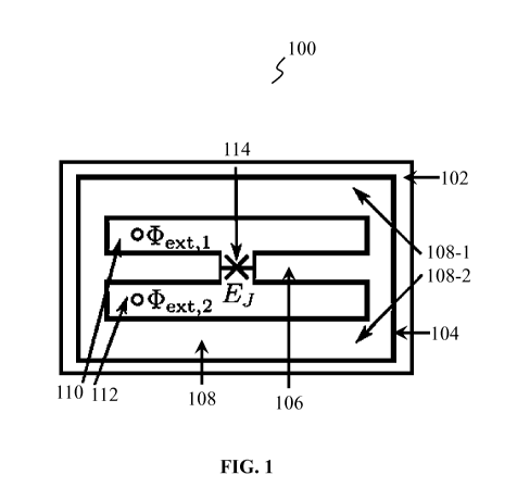
FIG. 1 shows a schematic top view of a QPU 100
in accordance with a first exemplary embodiment. As
shown in FIG. 1, the QPU 100 comprises a dielectric
CA 03200097 2023-04-27
WO 2022/129693
PCT/F12021/050872
18
substrate 102 and a superconducting qubit 104 provided
on the dielectric substrate 102. In the first
embodiment, the superconducting qubit 104 is configured
as a CPW resonator comprising a center superconductor
106 and a superconducting ground plane 108. The
superconductor 106 is galvanically connected to the
superconducting ground plane 108 on a first pair of
opposite sides (i.e. left and right sides, as shown in
FIG. 1). At the same time, the superconductor 106 is
separated by equal gaps 110 and 112 from the
superconducting ground plane 108 on a second pair of
opposite sides (i.e. top and bottom sides, as shown in
FIG. 1). In this case, the superconductor 106 serves as
the linear inductive-energy element of the
superconducting qubit 104. As for the non-linear
inductive-energy element, it is represented by a single
Josephson junction 114 embedded in the superconductor
106 such that the QPU 100 is free of superconducting
islands. Here, a superconducting island may, refer to a
Cooper-pair box connected via a tunnel junction to the
center superconductor 106. As another example, a
superconducting island would be formed between two
Josephson junctions embedded in series within the center
conductor. It should be noted that all constructive
elements of the QPU 100 in FIG. 1 are not shown to scale
for convenience. Furthermore, the shape of the center
superconductor 106 and the superconducting ground plane
108 are also illustrative and may be modified, depending
on particular applications.
Although the superconducting qubit 104 is
configured as the CPW resonator, this should not be
construed as any limitation of the invention. In other
embodiments, the superconducting qubit 104 may be
configured as any type of a distributed-element
resonator (one example of which is the CPW resonator),
or the superconducting qubit 104 may be configured as
any other combination of the linear and non-linear
CA 03200097 2023-04-27
WO 2022/129693 PCT/F12021/050872
19
inductive-energy elements configured to be phase-biased
such that their quadratic potential energy terms are at
least partly cancelled by one another.
As for the Josephson junction 114, it may
interrupt the center superconductor 106, as shown in
FIG. 1. In one embodiment, the Josephson junction 114
may be embedded in the center superconductor 106 such
that a current flowing through the center superconductor
106 is equal on both sides of the Josephson junction
114. In another embodiment, the Josephson junction 114
is centrally arranged in the center superconductor 106.
To provide the above-mentioned cancellation,
the QPU 100 should also comprise a phase-biasing element
(not shown in FIG. 1). In the first embodiment, the
phase-biasing element is intended to be configured to
generate and thread a magnetic flux cDoextj and clip
-ext2
through the gaps, i.e., loops, 110 and 112, thereby
providing phase biasing in a proper manner. Thanks to
the two parallel loops, the superconducting qubit 104
is gradiometric, meaning that it is protected against
flux noise whose spatial scale exceeds the width of the
superconducting qubit 104. This phase biasing leads to
at least partial mutual cancellation of the quadratic
potential energy terms of the superconductor 106 and the
Josephson junction 114, thereby improving the
anharmonicity of the superconducting qubit 104. The
phase-biasing element may comprise one or more coils
and/or one or more flux-bias lines for providing
magnetic flux control. The flux-bias line may be
implemented as a superconducting wire on the dielectric
substrate 102, and magnetic fields may be generated by
tuning a current flowing through the wire. In some other
embodiments, such a phase-biasing element may be
configured to provide the phase biasing by applying a
suitable voltage to the Josephson junction 114, instead
of or in addition to threading the magnetic field
through the gaps 110 and 112.
CA 03200097 2023-04-27
WO 2022/129693 PCT/F12021/050872
Since the Josephson junction 114 is embedded
in the CPW resonator such that no isolated
superconducting islands are formed, the inductance and
the capacitance of the CPW resonator shunt the Josephson
5 junction 114 and provide protection against dephasing
arising from low-frequency charge noise. Due to the
inductive shunt, the superconducting qubit 104 should
be fully immune to the low-frequency charge noise due
to its topology unlike the commonly employed transmon
10 qubits, where only the few lowest energy levels are well
protected against charge noise.
As can be seen in FIG. 1, the superconducting
ground plane 108 comprises opposite upper and lower
portions 108-1, 108-2 which are physically separated
15 from each other by the center superconductor 106 and the
gaps 110, 112. In one embodiment, these opposite
portions may be connected with each other via air
bridges stretching over the center superconductor 106
and gaps 110, 112 in order to suppress parasitic slot
20 line modes of the CPW resonator.
FIG. 2 shows a circuit model 200 used for
deriving the Hamiltonian of the superconducting qubit
104 included in the QPU 100 when it is subjected to an
external magnetic flux. According to the circuit model
200, the CPW resonator of length 21 is modeled by using
N lumped element inductors and capacitors.
Additionally, the Josephson junction 114 is assumed to
be arranged between capacitors 202 and 204 with indices
J and J+1. Due to the gradiometric nature of the two
loops, the external magnetic flux in the following
calculations is regarded as the (scaled) difference of
the external magnetic fluxes on the two sides of the
center superconductor 106, i.e. Paw = (CDext,2¨ (1)ext, 1)/2. By
using the circuit model 200, it is possible to write a
classical kinetic energy term T and a potential energy
term U for the circuit as
CA 03200097 2023-04-27
WO 2022/129693 PCT/F12021/050872
21
1 1 2
T=cttAx + - C - 11JJ) ,
2
1 2 1
U = __ ( + CDdiff,1) (w1CDdiff,32
21totAX 21totAX i=2,ti#J+1
1 2
240tAX 27E ,
CDdiff,N) ¨ Ej cos ¨ (Wpm_ ¨ ,
4$0
where N[Ji =j Vie0dT is the node flux across the i-th
capacitor with voltage VL,Odiffj is the external magnetic
flux across the i-th loop, Ax=211N is the length scale
for discretization, ctot is the total capacitance per
unit length of the CPW resonator, /tot is the total
inductance per unit length of the CPW resonator, El is
the Josephson energy, CJ is the capacitance of the
Josephson junction 114, and c100 is the flux quantum as
above. Additionally, the dots over the symbols denote
time derivatives.
Using the Lagrangian formalism, one may then
derive the classical equation of motion for the node
fluxes within the CPW resonator. In the continuum limit
one may obtain the following result:
1
atotlij = axx0 - axBdiff,
utot utot
where Ti-,0(x) corresponds to the continuum limit of the
node flux at location xi, cDdiff,i/(sAx) ->Bdiff denotes the
effective magnetic field difference, and s is the
distance between the center superconductor 106 and the
superconducting ground plane 108. Using the Lagrangian
formalism, one may also derive a boundary condition for
the node flux at the location xF corresponding to the
left electrode of the Josephson junction 114:
27c 1 cliff
¨I Sin = ax - Olxx
tot -J 211t0t'
CA 03200097 2023-04-27
WO 2022/129693
PCT/F12021/050872
22
where A4Y= Wpm_ ¨11JJ is the branch flux across the
Josephson junction 114, /c=27-cEj/cDo is the critical
current of the Josephson junction 114, and cDdiff=EicDdiffj
is the total external magnetic flux difference. In the
above equation, the assumption of a homogenous magnetic
field has been utilized to write(Pdiffj/Ax-->Odiff/(20, where
21 is the length of the center superconductor 106. Note
that a similar boundary condition may be derived for the
right electrode of the Josephson junction 114.
Additional boundary conditions O(-1) =0 and OM =0 arise
from the grounding of the center superconductor 106.
Based on the classical equation of motion and
the boundary conditions, it follows that the (classical)
generalized flux may be described as a linear
combination of a dc supercurrent and an infinite number
of oscillatory normal modes, namely:
-0(x, t) = 00u0(x) uõ (x) (t),
7/?1_
where 00 is the time-independent coefficient of the "dc
mode", and u000 is the corresponding envelope function.
In intuitive terms, the dc supercurrent biases the
Josephson junction 114, which changes the effective
Josephson inductance seen by the oscillatory (ac) normal
modes. Here, {itn(x)} are the envelope functions of the
oscillatory ac modes and {On00} are the corresponding
time-dependent coefficients. Importantly, the envelope
functions and the corresponding mode frequencies may be
derived using the above equation of motion and the above
boundary conditions.
To use the CPW resonator with the embedded
Josephson junction 114 as the superconducting qubit 104,
one should observe that the non-linearity of the
Josephson junction 114 turns some of the normal modes
into anharmonic oscillators. In the following, we focus
on the nt¨th mode and assume that we would like to
CA 03200097 2023-04-27
WO 2022/129693
PCT/F12021/050872
23
operate it as the qubit. With this in mind, it is
possible to derive a single-mode approximation for the
quantum Hamiltonian that is given by
Pm = 4E,,((p0)11,22 + -21 EL,m (q)0)(Pin2 + EL Om ((Pdiff (PO) ¨ Ej COS (Om ¨
(Po)
where Qm((po) is the effective charging energy
associated with the tn¨th mode, Am is the charge
operator of the tn¨th mode, EL,m((p0) is the effective
inductive energy of the rn-th mode, Om is the phase
operator corresponding to the rn-th mode, EL =
06/(202/(2//t0t) is the inductive energy associated with
the total linear inductance of the CPW resonator,(po=
27r00/00 is the phase bias corresponding to the dc
current, and (pdiff=27ECDdiffiCD0 denotes the phase associated
with the external magnetic flux. Note that the phase and
charge operators are conjugate operators satisfying the
commutation relation [mdim] =i, where i is the imaginary
unit.
It should be noted that the at¨th mode of the
superconducting qubit 104 is treated quantum-
mechanically in the above Hamiltonian, but the dc
Josephson phase (po is treated as a static variable that
is computed based on a semiclassical theory. According
to the semiclassical theory, the dc Josephson phase is
given by the following flux quantization condition:
27E Odiff
/c sin (-00) + ___________________________
cDo 2tot 2tot'
where =
cDo(Po/(27r) is the branch flux associated with
the dc Josephson phase.
In general, the anharmonicity am/(270 of a
given mode may be computed numerically by performing the
following steps:
CA 03200097 2023-04-27
WO 2022/129693
PCT/F12021/050872
24
- at first, determining the dc Josephson phase
using the above-given flux quantization condition;
- then, solving the (classical) normal mode
frequencies using the following equation that has been
derived from the above equation of motion and the above
boundary conditions:
2
kml cos (km(xj ¨ 1)) cos (km(xj + 1)) (Cj (km1)
atoti
¨
Itoti os(27c00)
¨ c ) sin(2km1) = 0,
LI 06
where km= w
m atotitot is the wavenumber of the rn-th mode,
and /I =c1:00/(27r/c) is the effective Josephson inductance;
and
- finally, numerically diagonalizing the
single-mode Hamiltonian Pm to obtain the quantized
energy spectrum of the mode of interest for a given
external magnetic flux. Using the energy spectrum of the
nt¨th mode, it is straightforward to evaluate the qubit
frequency wq/(270 and the corresponding anharmonicity
am/(270.
Due to the large capacitance per unit length
of the CPW resonator, the anharmonicity of the
superconducting qubit 104 is only modest unless the
parameters of the circuit model 200 are chosen suitably,
and an appropriate external magnetic flux is applied.
However, if the external magnetic flux equals half of
the flux quantum, i.e., cDdiff/cDo = +0.5, the dc Josephson
phase equals (pc, = +7T assuming that the Josephson
inductance is larger than the total inductance of the
CPW resonator. If the linear inductance of the CPW
resonator is only slightly smaller than the Josephson
inductance, the quadratic potential energy terms
associated with the inductive energy Elm(coo) and the
Josephson energy E./ cancel each other almost completely,
which can result in a large anharmonicity. Using
CA 03200097 2023-04-27
WO 2022/129693
PCT/F12021/050872
experimentally attainable values of the parameters for
the circuit model 200, the present authors have found
that the anharmonicity of the lowest-frequency mode may
(greatly) exceed 500 MHz for a qubit frequency of
5 approximately 5 GHz if the external magnetic flux is
tuned to cDdiffjcPc, = 0.5. It is necessary to note that this
also corresponds to a flux-insensitive sweet spot
protecting the superconducting qubit 104 against the
dephasing induced by the flux noise. Some numerical
10 results are illustrated in FIGs. 3-7.
More specifically, FIG. 3 shows the DC
Josephson phase (pc, as a function of the external
magnetic flux difference cDdiff for one possible inductance
ratio 2//t0t/Lj =Lcpw/Lj = 0.77 . FIG. 4 shows frequencies fm=
15 com/(270 of the 4 lowest frequency normal modes as a
function of the external magnetic flux cDdiff. FIG. 5 shows
anharmonicities and (27-c) of the 4 lowest frequency normal
modes as a function of the external magnetic flux cDdiff.
Note the large anharmonicity (>500 MHz) of the lowest
20 frequency mode at cDdifficik, = 0.5 . FIG. 6 shows a potential
energy landscape U ((pm) and phase-basis wavefunctions for
the 4 lowest energy states of the lowest-frequency
normal mode at cDdiffjcPc, = 0.5 . FIG. 7 shows a close-up of
the anharmonicity (27-c) and qubit frequency coq/(270
25 associated with the lowest frequency normal mode around
cDdiff/cDo P=-=-= 0.5 . Note that cDdiff/cDo = 0.5 corresponds to a flux-
insensitive sweet spot with these parameter values. The
parameters used to obtain the numerical results shown
in FIGs. 3-7 correspond to the parameter set given in
Table 1 below:
CA 03200097 2023-04-27
WO 2022/129693
PCT/F12021/050872
26
Table 1. Exemplary parameters used to estimate the
frequencies and anharmonicities of the normal modes in
the superconducting qubit 104 subjected to an external
magnetic flux.
214m) I. P Hz C iIkj (õq c,,,.(1)171m)
PaTameter 34A &t,'? 20.0 1.4 0.08 5.2 74
1, (iH/ni 1.fAillm.) U/ia) Zo (Q.) 211/L3
Pffl'aillet(TSa 0.78 OA OfN 103 0.77
In Table 1, 11//C[-1,1] is the (relative)
location of the Josephson junction 114 in the center
superconductor 106 (xj// = 0 corresponds to the Josephson
junction 114 centrally located in the center
superconductor 106), ko = w/(w + 2s) is the
ratio
describing the geometry of the CPW resonator, w is the
width of the center superconductor 106, s is the gap
between the center superconductor 106 and the
superconducting ground plane (i.e. the gap 110 or 112),
Eeff is the effective permittivity of the CPW resonator,
/k is the kinetic inductance per unit length of the
resonator, and /g is the geometric inductance per unit
length of the resonator. Furthermore, Z
-o = Vito-tic-tot is the
characteristic impedance of the CPW resonator.
To improve the anharmonicity further, one may
fabricate the center superconductor 106 of the CPW
resonator from a superconducting material with a high-
kinetic inductance, such as a superconducting thin film.
This would increase the inductance of the CPW resonator
with respect to the capacitance. As a result, the total
capacitance of the CPW resonator could be reduced, which
would improve the anharmonicity of the superconducting
qubit 104. In such a circuit model, the anharmonicity
could exceed 200 MHz even in the absence of an external
magnetic flux, and greatly exceed 1 GHz with the
external magnetic flux. However, superconducting thin
CA 03200097 2023-04-27
WO 2022/129693 PCT/F12021/050872
27
films tend to be relatively lossy and, therefore, the
increase in the anharmonicity might be accompanied by a
significant decrease in the relaxation and coherence
times. For this reason, the approach based on an
external flux without any superconducting thin films
seems the most promising path towards a high-coherence
high-anharmonicity superconducting qubit.
FIGs. 8A and 8B show schematic capacitive and
inductive couplings between superconducting qubits in
accordance with the first exemplary embodiment. More
specifically, FIG. 8A shows a schematic top view of a
QPU 800 comprising a combination of two superconducting
qubits 104 capacitively coupled to each other. FIG. 8B
shows a schematic top view of a QPU 802 comprising a
combination of three superconducting qubits 104
inductively coupled to each other. In FIGs. 8A and 8B,
the white color denotes the center superconductor 106,
the superconducting ground plane 108 and the Josephson
junction 114 in each superconducting qubit 104, while
the black color denotes the gaps 110 and 112 in each
superconducting qubit 104. It should be apparent to
those skilled in the art that the number of the
superconducting qubits 104 shown in FIGs. 8A and 8B is
for illustrative purposes only and should not be
construed as any limitation of the invention. Moreover,
it should be again noted that the size of the QPUs 800
and 802 and their constrictive elements are not shown
to scale for convenience.
FIG. 9 shows a schematic top view of a QPU 900
in accordance with a second exemplary embodiment.
Similar to the QPU 100 in the first exemplary
embodiment, the QPU 900 comprises a dielectric substrate
902 and a superconducting qubit 904 provided on the
dielectric substrate 902. In the second embodiment, the
superconducting qubit 904 is also configured as a CPW
resonator comprising a center superconductor 906 and a
superconducting ground plane 908. The superconductor 906
CA 03200097 2023-04-27
WO 2022/129693 PCT/F12021/050872
28
is galvanically connected to the superconducting ground
plane 908 on a first pair of opposite sides (i.e. left
and right sides, as shown in FIG. 9). At the same time,
the superconductor 906 is separated by equal gaps 910
and 912 from the superconducting ground plane 908 on a
second pair of opposite sides (i.e. top and bottom
sides, as shown in FIG. 9). The superconductor 906
serves as the linear inductive-energy element of the
superconducting qubit 904. Contrary to the first
embodiment, the non-linear inductive-energy element in
the second embodiment is represented by a combination
of two parallel Josephson junctions 914 and 916 embedded
in the superconductor 906 such that the QPU 900 is free
of superconducting islands. Such an arrangement of the
Josephson junctions 914 and 916 forms a SQUID loop,
where the phase biasing may be provided by threading a
magnetic field through the gaps 910 and 912 and the
SQUID loop. It should be again noted that all
constructive elements of the QPU 900 are shown in FIG.
9 not to scale for convenience. Furthermore, the shape
of the center superconductor 906 and the superconducting
ground plane 908 are also illustrative and may be
modified, depending on particular applications.
FIG. 10 shows a schematic top view of a QPU
1000 in accordance with a third exemplary embodiment.
Similar to the QPU 100 in the first embodiment and the
QPU 900 in the second embodiment, the QPU 1000 comprises
a dielectric substrate 1002 and a superconducting qubit
1004 provided on the dielectric substrate 1002. In the
third embodiment, the superconducting qubit 1004 is also
configured as a CPW resonator comprising a center
superconductor 1006 and a superconducting ground plane
1008. The superconductor 1006 is galvanically connected
to the superconducting ground plane 1008 on a first pair
of opposite sides (i.e. left and right sides, as shown
in FIG. 10). At the same time, the superconductor 1006
is separated by equal gaps 1010 and 1012 from the
CA 03200097 2023-04-27
WO 2022/129693 PCT/F12021/050872
29
superconducting ground plane 1008 on a second pair of
opposite sides (i.e. top and bottom sides, as shown in
FIG. 10). The superconductor 1006 serves as the linear
inductive-energy element of the superconducting qubit
1004. Contrary to the first and second embodiments, the
non-linear inductive-energy element in the third
embodiment is represented by a combination of three
Josephson junctions 1014, 1016 and 1018. The Josephson
junction 1014 is embedded in the center superconductor
1006, while the Josephson junctions 1016 and 1018 are
arranged in the top gap 1010 in the vicinity of the
Josephson junction 1014 such that the Josephson
junctions 1016 and 1018 connect the center
superconductor 1006 to the ground plane 1008. The shown
arrangement of the Josephson junctions 1014, 1016 and
1018 is not limitative and may be modified, depending
on particular applications. For example, one of the
Josephson junctions 1016 and 1018 may be omitted or may
be arranged in the other bottom gap 1012 in the vicinity
of the Josephson junction 1014. What is important is
that the Josephson junctions 1014, 1016 and 1018 are
again embedded in the superconducting qubit 1004 such
that the QPU 1000 is free of superconducting islands.
In the meantime, the phase biasing may be provided by
the same manner as in the first embodiment, i.e. by
threading the magnetic field through the gaps 1010 and
1012. It should be again noted that all constructive
elements of the QPU 1000 in FIG. 10 are not shown to
scale for convenience. Furthermore, the shape of the
center superconductor 1006 and the superconducting
ground plane 1008 are also illustrative and may be
modified, depending on particular applications.
FIG. 11 shows a schematic top view of a QPU
1100 in accordance with a fourth exemplary embodiment.
Similar to the QPU 100 in the first embodiment, the QPU
900 in the second embodiment, and the QPU 1000 in the
third embodiment, the QPU 1100 comprises a dielectric
CA 03200097 2023-04-27
WO 2022/129693 PCT/F12021/050872
substrate 1102 and a superconducting qubit 1104 provided
on the dielectric substrate 1102. In the fourth
embodiment, the superconducting qubit 1104 is also
configured as a CPW resonator comprising a center
5 superconductor 1106 and a superconducting ground plane
1108. The superconductor 1106 is galvanically connected
to the superconducting ground plane 1108 on a first pair
of opposite sides (i.e. left and right sides, as shown
in FIG. 11). At the same time, the superconductor 1106
10 is separated by equal gaps 1110 and 1112 from the
superconducting ground plane 1108 on a second pair of
opposite sides (i.e. top and bottom sides, as shown in
FIG. 11). The superconductor 1106 serves as the linear
inductive-energy element of the superconducting qubit
15 1104. Contrary to the first, second and third
embodiments, the non-linear inductive-energy element in
the fourth embodiment is represented by a combination
of five Josephson junctions 1114, 1116, 1118, 1120 and
1122. The Josephson junction 1114 is embedded in the
20 center superconductor 1106, while the Josephson
junctions 1116-1122 are arranged in the gaps 1110 and
1112 in the vicinity of the Josephson junction 1114 such
that the Josephson junctions 1116 and 1118 connect the
center superconductor 1106 to the ground plane 1108 via
25 the top gap 1110, and the Josephson junctions 1120 and
1122 connect the center superconductor 1106 to the
ground plane 1108 via the bottom gap 1112. The shown
arrangement of the Josephson junctions 1114-1122 is not
limitative and may be modified, depending on particular
30 applications. For example, one or more of the Josephson
junctions 1116-1122 may be omitted. What is important
is that the Josephson junctions 1114-1122 are again
embedded in the superconducting qubit 1104 such that the
QPU 1100 is free of superconducting islands. In the
meantime, the phase biasing may be provided by the same
manner as in the first and third embodiments, i.e. by
threading the magnetic field through the gaps 1110 and
CA 03200097 2023-04-27
WO 2022/129693
PCT/F12021/050872
31
1112. It should be again noted that all constructive
elements of the QPU 1100 are shown in FIG. 11 not to
scale for convenience. Furthermore, the shape of the
center superconductor 1106 and the superconducting
ground plane 1108 are also illustrative and may be
modified, depending on particular applications.
In the third and fourth embodiments, if there
is an even number of Josephson junctions arranged in the
gaps between the center superconductor and the
superconducting ground plane, these Josephson junctions
may be arranged symmetrically or asymmetrically relative
to the Josephson junction embedded in the center
superconductor, depending on particular applications.
In some other embodiments, the QPU (e.g., any
of the QPUs 100, 900-1100) further comprises signal
lines provided on the dielectric substrate. The signal
lines may be used to provide (e.g., from an external
control unit or control electronics if the QPU is used
in the quantum computer) control signals to the
superconducting qubit(s). The signal lines may comprise
radio-frequency lines, and the control signals may
comprise microwave pulses. The control signals may allow
one to control the superconducting qubit(s) in a desired
manner.
In some other embodiments, the QPU (e.g., any
of the QPUs 100, 900-1100) further comprises readout
lines provided on the dielectric substrate. The readout
lines may be included in the QPU in combination with the
signal lines. The readout lines may be coupled to the
superconducting qubit(s) via readout resonators. The
readout lines may be used to take state measurements of
the superconducting qubit(s), if required.
Although the exemplary embodiments of the
invention are described herein, it should be noted that
various changes and modifications could be made in the
embodiments of the invention, without departing from the
scope of legal protection which is defined by the
CA 03200097 2023-04-27
WO 2022/129693 PCT/F12021/050872
32
appended claims. In the appended claims, the word
"comprising" does not exclude other elements or
operations, and the indefinite article "a" or "an" does
not exclude a plurality. The mere fact that certain
measures are recited in mutually different dependent
claims does not indicate that a combination of these
measures cannot be used to advantage.