Note: Descriptions are shown in the official language in which they were submitted.
CA 03200882 2023-05-04
WO 2022/101507
PCT/EP2021/081871
1
Antenna system
Description
Technical Field
The present invention relates to an antenna system in general, and more
specifically, to an antenna system comprising transparent antenna arrangement.
Thus, the invention concerns multiple domains where an antenna system is
used.
Background Art
Mobile data traffic is increasing continuously and will boom significantly
with 5G,
putting mobile network operators under CAPEX pressure. Higher frequency bands
for 5G mean more challenges for coverage deployment, especially in dense urban
areas where capacity will be needed and strict EMF limitations apply. The
deployment of small cells are described as a good solution for capacity
improvement
which requires to install a large number of antennas in order to stably
perform
electromagnetic wave transmission and reception. However, many drawbacks limit
the deployment of small cells. First, it is very difficult to find location
for new
antennas. Second, bringing fiber and electricity outdoor is costly. Finally,
urbanistic
regulations may limit possibilities for small cells.
On the other hand, In recent years with miniaturization, antennas are
increasingly installed in buildings. When installing the antenna in the
building, it is
necessary to select the proper placement of the antenna so that
electromagnetic
waves can be transmitted and received stably while preventing the appearance
of
the building from being impaired.
US 5,322,143 describes a planar antenna having three conductive layers: a
patch network, a ground and feeding network. The planar antenna can be
integrated
into a façade of a building using the glass panel as a carrier. The issue with
such
planar antennas, because integrated into the façade, is that at least the
electrical
connection, the installation and the maintenance is complicated and impossible
to
manage once the façade is on the building. On top of that, performance
parameters
of the planar antenna is limited by thicknesses of the components of the
façade,
such as glass panels, spacers,...
CA 03200882 2023-05-04
WO 2022/101507
PCT/EP2021/081871
2
Therefore, with such planar antennas is not possible to change the frequency
band or the optimize the transmission and / or reception of the antenna to
meet the
requirement of current and future communication systems.
.. Summary of invention
The present invention relates, in a first aspect, to antenna system inscribed
in a
parallelepiped. The parallelepiped has an antenna system front face. The
antenna
system comprises a first transparent dielectric panel in front of the antenna
system
front face and a second transparent dielectric panel in front of the first
transparent
dielectric panel and separated by at least one panel interlayer from the first
transparent dielectric panel. The antenna system also comprises a transparent
antenna arrangement comprising a patch network attached and separated by at
least one patch interlayer from the first transparent dielectric panel, a
feeding
network attached and separated by at least one feed interlayer from the second
transparent dielectric panel and a ground plane. The antenna system also
comprises an antenna housing.
The solution as defined in the first aspect of the present invention is based
on
that the antenna housing comprises a first retaining means to retain the first
transparent dielectric panel at a defined distance, Daf11, from the front
face.
The solution as defined in the first aspect of the present invention is also
based
on that at least one patch interlayer is a transparent polymer interlayer.
The present invention relates, in a second aspect, to a method to optimize the
transmission and / or the reception of an antenna system, according to the
first
aspect. The method comprises a step of defining the configuration of the
window
and / or the operating frequency and a step of adapting the distance Daf11 in
the
antenna housing.
Finally, the present invention also relates, in a third aspect, to the use of
an
antenna housing of an antenna system according to the first aspect to optimize
the
transmission and / or the reception of the antenna system mounted in front of
a
window.
It is noted that the invention relates to all possible combinations of
features
recited in the claims or in the described embodiments.
The following description relates to building applications but it's understood
that
CA 03200882 2023-05-04
WO 2022/101507
PCT/EP2021/081871
3
the invention may be applicable to others fields like automotive or
transportation
applications.
Brief description of the drawings
This and other aspects of the present invention will now be described in more
detail, with reference to the appended drawings showing various exemplifying
embodiments of the invention which are provided by way of illustration and not
of
limitation. The drawings are a schematic representation and not true to scale.
The
drawings do not restrict the invention in any way. More advantages will be
explained
with examples.
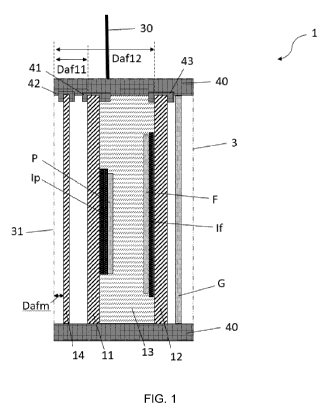
FIG. 1 is a schematic sectional view of an antenna system according to the
invention.
FIG. 2 is a schematic sectional view of antenna arrangement according to some
embodiments of the invention.
FIG. 3 is a schematic sectional view of antenna arrangement according to some
embodiments of the invention.
FIG. 4 is a schematic 3D view of an antenna system according to a first
embodiment mounted on a window.
FIG. 5 is a schematic side view of an antenna system according to a first
embodiment.
FIG. 6 is a schematic teardown view of an antenna system according to a first
embodiment.
FIG. 7 is a schematic 3D view of an antenna system according to a second
embodiment mounted on a window.
FIG. 8 is a schematic side view of an antenna system according to a second
embodiment.
Detailed description
It is an object of the present invention to alleviate the above described
problems
and to remove the barriers to outdoor 4G and 5G network densification.
Especially,
the object of the first aspect of the present invention is to allow indoor
installation of
the antennas, eliminating the need for scaffolding or foundation work in the
street.
Another advantage of the present invention is that transparent antenna enables
CA 03200882 2023-05-04
WO 2022/101507
PCT/EP2021/081871
4
seamless indoor or outdoor placement in line with urban aesthetics and EMF
constraints.
Another advantage of the present invention is to provide an efficient antenna
system in front of a window as discrete as possible meaning that the antenna
system
is transparent or at least the antenna arrangement is transparent.
According to a first aspect of the invention, the invention relates to antenna
system 1 inscribed in a parallelepiped 3. The parallelepiped has an antenna
system
front face 31.
Antenna system according to the invention have typically a weight of about 2
kg
to 3 kg. The parallelepiped has typically a width and / or a length comprised
between
mm to 600 mm for example a rectangular shape of 210 mm x 250 mm, a
rectangular shape of 150 mm x 160 mm or rectangular shape of 255 mm x 500
mm depending of the operating frequencies, the number of antenna arrangements,
the number of elements comprised in the antenna arrangement and / or the
15 transparency design.
Preferably, the antenna system works for 4G and / or 5G, meaning wavelengths
with frequencies from 690 MHz to 70 GHz.
The antenna system 1 comprises a first transparent dielectric panel 11 and a
second transparent dielectric panel 12. The first transparent dielectric panel
is in
20 front of the antenna system front face 31. The second transparent
dielectric panel
12 is in front of the first transparent dielectric panel 11.
The term "transparent" denotes a property illustrating the average TL (light
transmission) of visible light transmitted through a material in the visible
spectrum
of at least 1%. Preferably, transparent relates to a TL property of at least
10%. More
preferably, transparent denotes a TL of at least 50%. Ideally, transparent
denotes a
TL of at least 70%.
A dielectric panel is a panel that is not electrically conductive.
The first and the second transparent dielectric panels can have different
chemical composition, such as plastic-based composition. The plastic-based
composition can be PET, polycarbonate, PVC or any other transparent dielectric
plastic-based that can be used as a panel.
Preferably, the first and / or the second transparent dielectric panel
comprises
a glass panel to protect the antenna arrangement and the antenna system from
CA 03200882 2023-05-04
WO 2022/101507
PCT/EP2021/081871
scratches. The glass panel can comprises at least 50 % in weight of SiO2 such
as
glass like soda lime glass, aluminosilicate glass or borosilicate glass.
In some embodiments, the first and the second transparent dielectric panels
have the same chemical composition to reduce the handling and the process of
5 .. manufacturing.
Preferably, the first and the second transparent dielectric panels can have a
loss
tangent equals to or smaller than 0.03 and more preferably the loss tangent of
the
dielectric panels is equal to or smaller than 0.02 and more preferably the
loss
tangent of the dielectric panels is equal to or smaller than 0.01 to reduce
the energy
loss in panels while increasing the antenna system efficiency.
In preferred embodiments, the first and the second transparent dielectric
panels
have a loss tangent equals to or smaller than 0.005 and more preferably the
loss
tangent of the dielectric panels is equal to or smaller than 0.003 to reduce
the energy
loss in panels while increasing the antenna system efficiency.
Preferably, the first and the second transparent dielectric panels are
borosilicate glass panels to reduce the loss tangent to a value equals to or
is smaller
than 0.01.
The dielectric panels can be manufactured by a known manufacturing method
such as a float method, a fusion method, a redraw method, a press molding
method,
or a pulling method. As a manufacturing method of the glass panel, from the
viewpoint of productivity and cost, it is preferable to use the float method.
Each transparent dielectric panel can be independently processed and / or
colored,... and / or have different thickness in order to improve the
aesthetic, safety,
Each transparent dielectric panel can be processed, i.e. annealed,
tempered,...
to respect the specifications of security requirements. The transparent
dielectric
panel can independently be a clear or a colored transparent dielectric panel,
tinted
with a specific composition or by applying an additional coating or a plastic
layer for
example.
The first and the second transparent dielectric panels can have any shape. The
shape of the transparent dielectric panels 11, 12 in a plan view is not
limited to a
rectangle and may be a trapeze, a triangle, a square, a circle or the like.
The first 11 and the second 12 transparent dielectric panels are separated by
at
CA 03200882 2023-05-04
WO 2022/101507
PCT/EP2021/081871
6
least one panel interlayer 13.
In some embodiments, the first 11 and the second 12 transparent dielectric
panels can be separated to create a space 13 filled by a gas like Air. In such
embodiments, the at least one panel interlayer 13 is the gas gap. Being
understood
that the first 11 and the second 12 transparent dielectric panels can be
separated
by the gas gap and at least one another interlayer.
In some embodiments, the first 11 and the second 12 transparent dielectric
panels can be laminated together. In such embodiments, the at least one panel
interlayer 13 is a interlayer able to laminate the first 11 and the second 12
transparent dielectric panels together. Preferably, such panel interlayers can
be
transparent plastic interlayers. Transparent plastic interlayer can be
polyvinyl butyral
(PVB), ethylene-vinyl acetate (EVA), polymethyl methacrylate (PMMA), a
polycarbonate (PC), a polystyrene (PS), a polyvinyl chloride (PVC), a
polyamide
(PA), a polyetherimide (PEI), a polyethylene terephthalate (PET), a
polyurethane,
an acrylonitrile butadiene styrene copolymer (ABS), a styrene acrylonitrile
copolymer (SAN), a styrene methyl methacrylate copolymer (SMMA) and any
mixtures of these, a crosslinked resin, an ionoplast, an ionomer, a cyclo-
olefin
polymer (COP), cyclo-Olefin copolymer (COC) or an Optical Clear Adhesive
(OCA).
Crosslinked or cured resins are known to the skilled person and are three
dimensional polymer networks obtained by the crosslinking/curing of low
molecular
weight species either by reaction with a curing agent also known as
crosslinker or
upon exposure to heat, UV radiations (UV) or electron beam (EB). Non
exhaustive
examples of crosslinked resins are epoxy resins, polyurethane resins, UV or EB
curable resins. In the present invention, the precursors of the crosslinked
resin may
be transparent or not provided that the crosslinked resin is transparent.
Remark that some polymer mixtures, copolymers and some semi-crystalline
polymers can be opaque and non-transparent due to a dispersed phase or due to
the presence of crystallites. Hence it is possible that not all compositions
of the
listed polymers mentioned above are transparent. The person skilled in the art
is
capable to identify what composition is transparent and hence identify if a
given
polymer falls within the claimed transparent polymers.
The term "in front of" denotes that the first transparent dielectric panel is
facing
the antenna system front face, the second transparent dielectric panel is
facing the
CA 03200882 2023-05-04
WO 2022/101507
PCT/EP2021/081871
7
first transparent dielectric panel.
In some embodiments, the first transparent dielectric, the second transparent
dielectric and / or installation interface panel, if it presents, are not
parallel to each
other. Preferably, surfaces of the first and the second panels are parallel
and the
first 11 and the second 12 transparent dielectric panels are parallel and
aligned to
each other and parallel and aligned to the antenna system front face 31 to
simplify
the antenna system design and fabrication while decreasing the antenna system
profile.
Preferably, the antenna system radiates towards a specific direction through
the
antenna system front face to emit and /or receive through a window and to
cover
terminals outside a building for instance.
The antenna system 1 also comprises a antenna housing 40. The antenna
housing comprises a first retaining means 41 to retain the first transparent
dielectric
panel 11 at a defined distance, Daf11, from the front face 31.
In some embodiments, the antenna system 1 can comprise an installation
interface panel 14 located between the first dielectric panel 11 and the
antenna
system front face 31. The installation interface panel permits to cancels out
the
impact of the installation medium/media on the antenna system performance and
permits to maintain the impedance response of the antenna as well as the
radiation properties of the antenna within the specifications. In some
embodiments, the installation interface panel can add more functionalities to
the
antenna system, such as the beam steering or beam shaping.
The installation interface panel 14 can comprise at least a transparent
dielectric
panel such as glass and / or plastic. In some embodiments. At least a
conductive
pattern can be deposited on at least one of dielectric panels.
In some prefered embodiments, the antenna housing comprises a second
retaining means 42 to retain the installation interface panel 14 at a defined
distance, Dafm, from the antenna system front face 31.
Preferably, the installation interface panel 14 is parallel to the antenna
system
front face 31 to simplify the design and fabrication of the installation
interface
panel.
Preferably, in the second aspect of the present invention, the method
comprises
CA 03200882 2023-05-04
WO 2022/101507
PCT/EP2021/081871
8
a step of defining the configuration of the window and a step of adapting the
defined
distance Dafm in the antenna housing to optimize the reception and / or the
transmission of the antenna system.
In some embodiments, retaining means 41, 42, 43 can have a profile shape
adapted to retain the corresponding panel.
In some embodiments, the first 41 and the third 43 retaining means are a
single
retaining means to adapt in one step the defined distances Daf11 and Daf12
meaning that the defined distances Daf11 and Daf12 are adapted by the same
difference meaning that in case of Daf11 is adapted by a distance d, Daf12 is
also
adapted by the same distance d.
In some embodiments, the first and / or the second and / or the third
retaining
means can comprise an adjustable means to modify the defined distance between
the antenna system front face and respectively the first transparent
dielectric panel,
the matching panel and the second transparent dielectric panel to optimize the
reception and / or transmission of the antenna system.
In some embodiments, each retaining means can independently adapt the
defined distance Daf11, Dafm and Daf12.
Preferably, the defined distance Dafm is between 1 mm and-10 mm.
Preferably, the defined distance Daf11 is between 1/10 of the wavelength,
more preferably 1/8 of the wavelength, and 1/2 of the wavelength meaning that
preferably the defined distance Daf11 equals to or is higher than 10 mm for 4G
and 5G.
Preferably, the defined distance Daf12 is between equals to or is higher than
15
mm up to preferably 70 mm. it is understood that Dafm < Daf11 < Daf12.
Preferably, the difference between the patch network and the feeding network
is substantially comprises between 40 and 100 mm, more preferably is
substantially
comprises between 45 and 8 mm, and much more preferably is substantially
comprises between 48 and 68 mm.
In some preferred embodiments, the retaining means comprises a recess
wherein respectively the first transparent dielectric, the second transparent
dielectric
and / or installation interface panel is retained. In some embodiments, the
recess
can have a width larger than the thickness of the sum of thickness of the
corresponding the first transparent dielectric, the second transparent
dielectric and
CA 03200882 2023-05-04
WO 2022/101507
PCT/EP2021/081871
9
/ or installation interface panel with the layers attached to it to be able to
insert and
retain the panel.
In some embodiments, retaining means 41, 42, 43 can have a mobile part, such
a screw, able to adapt the corresponding defined distance Daf11, Dafm and
Daf12
inside the corresponding recess.
In some embodiments, to modify the defined distance, the retaining means can
allow to retain different panel thicknesses. By modifying the thickness of the
first
transparent dielectric, the second transparent dielectric and / or
installation interface
panel to optimize the transmission and / or the reception of the antenna
system.
The antenna system 1 also comprises a transparent antenna arrangement 10
comprising a patch network P attached and separated by at least one patch
interlayer 1p from the first transparent dielectric panel 11.
The at least one patch interlayer 1p is a polymer interlayer. Preferably,
transparent polymer interlayer can be polyvinyl butyral (PVB), ethylene-vinyl
acetate
(EVA), polymethyl methacrylate (PMMA), a polycarbonate (PC), a polystyrene
(PS),
a polyvinyl chloride (PVC), a polyamide (PA), a polyetherimide (PEI), a
polyethylene
terephthalate (PET), a polyurethane, an acrylonitrile butadiene styrene
copolymer
(ABS), a styrene acrylonitrile copolymer (SAN), a styrene methyl methacrylate
copolymer (SMMA) and any mixtures of these, a crosslinked resin, an ionoplast,
an
ionomer, a cyclo-olefin polymer (COP), cyclo-Olefin copolymer (COC) or an
Optical
Clear Adhesive (OCA).
Crosslinked or cured resins are known to the skilled person and are three
dimensional polymer networks obtained by the crosslinking/curing of low
molecular
weight species either by reaction with a curing agent also known as
crosslinker or
upon exposure to heat, UV radiations (UV) or electron beam (EB). Non
exhaustive
examples of crosslinked resins are epoxy resins, polyurethane resins, UV or EB
curable resins. In the present invention, the precursors of the crosslinked
resin may
be transparent or not provided that the crosslinked resin is transparent.
Remark that some polymer mixtures, copolymers and some semi-crystalline
polymers can be opaque and non-transparent due to a dispersed phase or due to
the presence of crystallites. Hence it is possible that not all compositions
of the
listed polymers mentioned above are transparent. The person skilled in the art
is
capable to identify what composition is transparent and hence identify if a
given
CA 03200882 2023-05-04
WO 2022/101507
PCT/EP2021/081871
polymer falls within the claimed transparent polymers.
It is understood that the patch network P can be attached to any of the
surfaces
of the first transparent dielectric panel 11. Preferably the patch network P
is attached
to the surface opposite to the surface facing the antenna system front face 31
to
5 achieve a
higher antenna performance and in parallel to protect the patch network
P from the exterior attack, such as moisture, scratches,..., as illustrated in
FIG. 1.
In some embodiments, the patch network P comprises at least one resonating
conductive element. Preferably, the length of the conductive element is
equivalent
to the half of the effective wavelength at the operation frequency.
10
Preferably, the dimensions of the surface of the patch network is smaller than
the surface of the first transparent dielectric panel.
In some embodiments, several patch networks can be attached to the first
transparent dielectric panel to have an antenna system transmitting and / or
receipting same or different frequencies. In such embodiments, patch networks
are
electrically isolated from each other.
The conductive element of the patch network can have any shape such as a
rectangular shape. In some embodiments in which the dual-polarized operation
is
desired, a circular or square shape is preferred. Preferably, the patch
network is
conductive patch network.
The patch network can be printed, glued, coated on the patch interlayer or
placed by any other methods able to non-removably place a patch network on an
interlayer on such as screen-printing, inkjet printing, deposition, glued
wire, copper
foil, copper mesh, etc.
In some embodiments, the patch network can printed, glued, coated on a
transparent layer to facilitate the attachment to the first transparent
dielectric panel
with the patch interlayer and the handling. Such transparent layers are
preferably
transparent polymer film. Preferably, transparent polymer film can be
polyvinyl
butyral (PVB), ethylene-vinyl acetate (EVA), polymethyl methacrylate (PMMA), a
polycarbonate (PC), a polystyrene (PS), a polyvinyl chloride (PVC), a
polyamide
(PA), a polyetherimide (PEI), a polyethylene terephthalate (PET), a
polyurethane,
an acrylonitrile butadiene styrene copolymer (ABS), a styrene acrylonitrile
copolymer (SAN), a styrene methyl methacrylate copolymer (SMMA) and any
mixtures of these, a crosslinked resin, an ionoplast, an ionomer, a cyclo-
Olefin
CA 03200882 2023-05-04
WO 2022/101507
PCT/EP2021/081871
11
copolymer (COO), cyclo-Olefin polymer (COP) or an Optical Clear Adhesive
(OCA).
Material of the patch network can be metal-based material such as Copper,
Silver, conductive metal alloys with or without plated material, such as gold,
or any
other material able to be electrically conductive and able to be placed on a
patch
interlayer or on a transparent layer.
The first retaining means 41 retains the first transparent dielectric panel 11
at a
defined distance, Daf11, from the front face 31. That means the patch network
is
also maintain at a defined distance corresponding to the sum between Daf11 and
the distance separating the patch network from the calculation point of Daf11
in the
first transparent dielectric panel.
The transparent antenna arrangement 10 also comprises a feeding network F
attached and separated by at least one feed interlayer If from the second
transparent dielectric12.
It is understood that the feeding network F can be attached to any of the
surfaces of the second transparent dielectric panel 12. Preferably the feeding
network F is attached to the surface facing the first transparent dielectric
panel 11
meaning that the surface facing also the antenna system front face 31 to
protect the
feeding network F from the exterior attack, such as moisture, scratches,...,
as
illustrated in FIG. 1.
In some embodiments, the feeding network comprises at least one conductive
element to transfer the signal between the antenna system input and the patch
network. Preferably, the width of the feeding network at the input side is in
such a
way to provide a characteristic impedance of about 50 Ohms.
In some embodiments in which that there are two or more conductive elements
in the patch network per each antenna system input, the feeding network can
distribute the energy among those above-mentioned conductive elements.
The feeding network can be printed, glued, coated on the feed interlayer or
placed by any other methods able to non-removably place a feeding network on
an interlayer on such as screen-printing, inkjet printing, deposition, glued
wire,
copper foil, copper mesh, etc.
In some embodiments, the feeding network can printed, glued, coated on a
transparent layer to facilitate the attachment to the second transparent
dielectric
panel with the feed interlayer and the handling. Such transparent layers are
CA 03200882 2023-05-04
WO 2022/101507
PCT/EP2021/081871
12
preferably transparent polymer film. Preferably, transparent polymer film can
be
polyvinyl butyral (PVB), ethylene-vinyl acetate (EVA), polymethyl methacrylate
(PMMA), a polycarbonate (PC), a polystyrene (PS), a polyvinyl chloride (PVC),
a
polyamide (PA), a polyetherimide (PEI), a polyethylene terephthalate (PET), a
polyurethane, an acrylonitrile butadiene styrene copolymer (ABS), a styrene
acrylonitrile copolymer (SAN), a styrene methyl methacrylate copolymer (SM MA)
and any mixtures of these, a crosslinked resin, an ionoplast, an ionomer, a
cyclo-
Olefin copolymer (COC), cyclo-Olefin polymer (COP) or an Optical Clear
Adhesive
(OCA).
Material of the feeding network can be metal-based material such as Copper,
Silver, conductive metal alloys with or without plated material, such as gold,
or any
other material able to be electrically conductive and able to be placed on a
feed
interlayer or on a transparent layer.
The transparent antenna arrangement 10 also comprises a ground plane G to
ensure good and correct functioning of the antenna system.
The location of the ground plane compared to the patch network and the feeding
network is important and can affect significantly the performance of the
antenna
system.
In some embodiments where the ground plane is located between the patch
network and the feeding network, the ground plane comprises at least one
optimized
shaped and sized slot to get the desired performances.
In some embodiments where the feeding network is located between the patch
network and the ground, the at least one optimized shaped and sized slot in
the
ground plane can be absent.
The choice of the configuration is a compromise between complexity and
performance.
The ground plane can be printed, glued, coated on a dielectric panel, on a
ground interlayer or on a transparent layer or placed by any other methods
able to
non-removably place a ground plane on a dielectric panel, on a ground
interlayer
or on a transparent layer such as screen-printing, inkjet printing,
deposition, glued
wire, copper foil, copper mesh, etc.
In some embodiments, the ground plane is separated by at least one ground
interlayer to the second transparent dielectric panel.
CA 03200882 2023-05-04
WO 2022/101507
PCT/EP2021/081871
13
In some embodiments, the ground interlayer can be a space filled of gas, such
an air gap. The ground plane can be printed, glued, coated on a third
transparent
dielectric panel or placed by any other methods able to non-removably place a
ground plane on a dielectric panel such as screen-printing, inkjet printing,
deposition, glued wire, copper foil, copper mesh, etc.. In some embodiments,
the
ground plane can attached and separated by at least one ground interlayer to
the
third transparent dielectric panel.
In some embodiments, the ground plane is attached and separated by at least
one ground interlayer to a third transparent dielectric panel. In such
embodiments,
the ground interlayer can be a transparent polymer interlayer. In some
embodiments, the fourth retaining means can be comprises on the antenna
housing
to retain the third transparent dielectric panel.
The ground plane can printed, glued, coated on a transparent layer to
facilitate
the attachment to the second or a third transparent dielectric panel with the
ground
interlayer and the handling. Such transparent layers are preferably
transparent
polymer film. Preferably, transparent polymer film can be polyvinyl butyral
(PVB),
ethylene-vinyl acetate (EVA), polymethyl methacrylate (PMMA), a polycarbonate
(PC), a polystyrene (PS), a polyvinyl chloride (PVC), a polyamide (PA), a
polyetherimide (PEI), a polyethylene terephthalate (PET), a polyurethane, an
acrylonitrile butadiene styrene copolymer (ABS), a styrene acrylonitrile
copolymer
(SAN), a styrene methyl methacrylate copolymer (SMMA) and any mixtures of
these, a crosslinked resin, an ionoplast, an ionomer, a cyclo-Olefin copolymer
(COC), cyclo-Olefin polymer (COP) or an Optical Clear Adhesive (OCA).
Material of the ground plane can be metal-based material such as Copper,
Silver, conductive metal alloys with or without plated material, such as gold,
or any
other material able to be electrically conductive and able to be placed on a
ground
interlayer or on a transparent layer.
In some preferred embodiments, as for the patch network and the feeding
network, to ensure the conductivity and transparency, the ground plane can be
designed using a Cu-mesh on the top of a transparent layer such as a PET
layer.
In some embodiments, other transparent layers can be used to separate, to
assemble and to laminate at least the patch network, the feeding network and /
or
the ground plane to the first and / or the second transparent dielectric panel
and / or
CA 03200882 2023-05-04
WO 2022/101507
PCT/EP2021/081871
14
a third transparent dielectric panel if exists. These layers are preferably
transparent
polymers.
Preferably, the transparent layers are low-loss transparent layers to reduce
the
losses of the antenna system.
FIGs. 2 and 3 illustrate some embodiments of a transparent antenna
arrangement according to the invention in which some layers are used to
separate,
to assemble and to laminate the patch network, the feeding network and / or
the
ground plane to the first and / or the second transparent dielectric panel.
In one embodiment, as illustrated in FIG. 2, the transparent antenna
arrangement 10 comprises a patch network P attached to and separated from the
first transparent dielectric panel 11, a glass panel, by a patch interlayer
1p. The patch
interlayer is a COC or a COP. A PET layer 201 then a COP layer 202 and a glass
layer 203 is attached to the patch network P to facilitate the handling and to
protect
the patch network P. The patch network P is laminated on the first transparent
dielectric panel 11 with patch interlayer 1p and the layers 201, 202 with the
glass
panel 203.
The patch network P, the feeding network F and the ground plane G are
individually assembled on a transparent layer 201, 207, 208 to facilitate the
attachment to the corresponding transparent dielectric panel. Preferably,
these
transparent layers are PET layers.
The transparent antenna arrangement 10 comprises a feeding network F
attached to and separated by from the second transparent dielectric panel 12
at a
feed interlayer If and a PET layer 207. The feed interlayer If is a cyclo-
Olefin
polymer. The ground plane G is attached to the second transparent dielectric
panel
12 by a ground interlayer lg. The ground plane G is located between the
feeding
network F and the first transparent dielectric panel 11. There is a PET layer
207
between the ground interlayer Ig and the feeding network F, meaning that the
feeding network F is laminated between the feed interlayer If and the PET
layer 207.
To protect the ground plane G and the feeding network F, a PET layer 208, a
COP
layer 206 and a glass layer 205 is attached to the second transparent
dielectric
panel 12. The feeding network F and the ground plane G are laminated together
with the feed interlayer If, the ground interlayer Ig to the second
transparent
dielectric panel 12. Preferably, when the ground plane G is positioned between
the
CA 03200882 2023-05-04
WO 2022/101507
PCT/EP2021/081871
feeding network and the patch network, the ground plane comprises at least one
slot.
This is understood that PET layers 201, 207, 208 , COP layers 202, 206 and /
or glass layer 203, 205 can be absent or made with another composition.
5 The first
11 and the second 12 transparent dielectric panels are separated by a
panel interlayer 204. The panel interlayer 204 is a space filled by a gas,
preferably
an air gap. The thickness of the air gap is defined to optimize a minimal
distance to
increase the coupling performances between the patch network and the feeding
network and a maximal distance to increase the wide band performances of the
10 antenna arrangement.
In this embodiments, the housing of the antenna system can retain the first
and
the second transparent dielectric panels independently meaning that the air
gap can
be modified or defined modifying the defined distances Daf11 and Daf12
independently to optimize the transmission and the reception of the antenna
system.
15 Table 1
illustrates an embodiment with specific thicknesses, in millimeters and
measured in the normal direction of the main surface, of the different layers
illustrated in FIG. 2 optimizing the reception and / or the transmission of
the antenna
system for LIE B1 and LIE B3. It is understood that different thickness values
can
be used for the same bands or for different bands.
CA 03200882 2023-05-04
WO 2022/101507
PCT/EP2021/081871
16
Layer Thickness Imm]
11 2,0
I p 0,4
0,1
201 0,1
202 0,4
203 0,7
204 4,8
205 0,7
206 0,4
207 0,1
0,1
Ig 0,8
0,1
208 0,1
If 0,4
12 1,1
Table 1
Fig. 3 shows an another embodiment of an antenna arrangement 10 of an
antenna system according to the invention.
The first 11 and the second 12 transparent dielectric panels are separated by
a
panel interlayer 302. The panel interlayer 302 is a transparent polymer
interlayer, a
cyclo-Olefin polymer meaning that the first and the second first 11 and the
second
12 transparent dielectric panels are laminated together by the panel
interlayer 302.
The thickness of the panel interlayer is defined to optimize a minimal
distance to
increase the coupling performances between the patch network and the feeding
network while a maximal distance to increase the wide band performances of the
antenna arrangement.
In such embodiments, only the defined distance Daf11 and the defined distance
Daf12 are adapted with the antenna housing with the same difference because
the
first and the second transparent dielectric panels are laminated together by a
fixed
thickness.
The feeding network F is located between ground plane G and the second
transparent dielectric panel 12.
The patch network P, the feeding network F and the ground plane G are
CA 03200882 2023-05-04
WO 2022/101507
PCT/EP2021/081871
17
individually assembled on a transparent layer 301, 303, 304. Preferably these
transparent layers are PET layers. The patch network P is attached to the
first
transparent dielectric panel 11 by the patch interlayer 1p. PET layers with
the part of
the antenna arrangement, the patch network, the feeding network or the ground
plane, are laminated together with the first 11 and the second 12 transparent
dielectric panels with interlayers and layers with the patch network, the
feed, the
ground and the panel interlayers meaning that the patch network P, the feeding
network F and the ground plane G are laminated together between the first 11
and
the second 12 transparent dielectric panels with respectively the patch
network, the
feed and the ground interlayers and layers.
Table 2 illustrates a embodiment with specific thicknesses, in millimeters and
measured in the normal direction of the main surface, of the different layers
illustrated in FIG. 3 optimizing the reception and the transmission of the
antenna
system for LTE B42, LTE B43, 5G NR n77 and / or 5G NR n78. It is understood
that
different thickness values can be used for the same bands or for different
bands.
Layer Thickness Prim]
11
1p 0,4
0,1
301 01
3Ci2 1,6
0,1
if 0,8
G 0,1
30. 0,1
1g ),4
I 12 1,1
Table 2
The thicknesses of the first and the second transparent dielectric panels can
be
different. The thickness can depend of the composition to increase the antenna
system efficiency.
CA 03200882 2023-05-04
WO 2022/101507
PCT/EP2021/081871
18
In some embodiments, when the first and the second dielectric panels are glass
panels, the thicknesses are equal to or higher than 0.05 mm, preferably the
thicknesses are equal to or higher than 0.5 mm and more preferably the
thicknesses
are equal to or higher than 1 mm, and the thicknesses are equal to or smaller
than
4 mm, preferably the thicknesses are equal to or smaller than 3 mm, and more
preferably the thicknesses are equal to or smaller than 2 mm.
In some preferred embodiments, retaining means are notches and / or slides
on the antenna frame. Said notch can have a thickness, measured parallel to
the
normal of the antenna system front face , at least equals to the thickness of
the
corresponding panel, with the attached layers, interlayer and part of the
antenna
arrangement, to be inserted in.
In some embodiments, the thickness of the notches is higher than the
thickness of the corresponding panel, with the attached layers, interlayer and
part
of the antenna arrangement, to be inserted in. In such embodiment, a clamping
means can be add to firmly retain the corresponding panel. In such
embodiments,
the defined distance Daf1 1, Daf12 and / or Dafm can be adapted by modifying
the
position of the clamping means or by adapting the thickness of the panel.
As the patch network is attached to the first transparent dielectric panel,
the
defined distance Daf1 1 regulates the distance between the patch network and
the
antenna system front frame.
As the feeding network is attached to the second transparent dielectric panel,
the defined distance Daf12 regulates the distance between the feeding network
and
the antenna system front frame and between the patch network and the feeding
network. The distance between the patch network and the feeding network can be
managed by the panel interlayer and / or the first and the third retaining
means to
optimize the antenna system performances. In some embodiments, the distance
between the patch network and the feeding network is managed by the thickness
of
the panel interlayer. This thickness can be managed by modifying the thickness
of
at least one panel, interlayer, layer of the antenna arrangement and / or by
modifying
the thickness of the transparent panel polymer interlayer or the space filled
by a gas.
Preferably, depending of the operating frequency, the distance between the
patch
network and the feeding network is comprises between 1 mm and 10 mm,
preferably
CA 03200882 2023-05-04
WO 2022/101507
PCT/EP2021/081871
19
between 3 mm and 7 mm, and more preferably between 4.8 mm and 6.8 mm.
In some embodiments where the installation interface panel exists, the defined
distance Dafm between the installation interface panel and the antenna system
front
frame regulates the distance between the installation interface panel and the
patch
network and / or the feeding network.
FIGs. 4 to 8 illustrates an antenna system 1 mounted on a window 2.
The window 2 can be a window used as a window to close an opening of the
stationary object, such as a building, or to close an opening of the mobile
object,
such a train, a boat,...
Windows are usually multi-glazed windows to increase thermal performances of
the window.
The multi-glazed window 2 can be at least partially transparent to visible
waves
for visibility, and natural or artificial light. The multi-glazed window is
made of
multiple panels separated by at least one interlayer, forming multiple
interfaces. The
panels therefore can be separated by a space filled with gas and / or by a
polymeric
interlayer.
In some embodiments, the multi-glazed window 2 can comprise at least two
glass panels separated by a spacer allowing to create a space filled by a gas
like
Argon to improve the thermal isolation of the multi-glazed window, creating an
insulating multi-glazed window. The invention is not limited to apparatus for
use on
multi-glazed window having two panels. The apparatus and method of the present
invention are suitable for any multi-glazed window such as double, triple
glazed
windows.
In some embodiments, the glass panel can be a laminated multi-glazed window
.. such as those to reduce the noise and / or to ensure the penetration
safety. The
laminated glazing comprises panels maintained by one or more interlayers
positioned between glass panels. The interlayers are typically polyvinyl
butyral
(PVB) or ethylene-vinyl acetate (EVA) for which the stiffness can be tuned.
These
interlayers keep the glass panels bonded together even when broken in such a
way
.. that they prevent the glass from breaking up into large sharp pieces.
Said panels of the multi-glazed window can be made of glass, polycarbonate,
PVC or any other material used for a window mounted on a stationary object or
on
a mobile object.
CA 03200882 2023-05-04
WO 2022/101507
PCT/EP2021/081871
Usually, the material of the panels of multi-glazed window 2 is, for example,
soda-lime silica glass, borosilicate glass, aluminosilicate glass or other
materials
such as thermoplastic polymers or polycarbonates which are especially known
for
automotive applications. References to glass throughout this application
should not
5 .. be regarded as limiting.
The multi-glazed window 2 can be manufactured by a known manufacturing
method such as a float method, a fusion method, a redraw method, a press
molding
method, or a pulling method. As a manufacturing method of the multi-glazed
window, from the viewpoint of productivity and cost, it is preferable to use
the float
10 method.
Each panel can be independently processed and / or colored,... and / or have
different thickness in order to improve the aesthetic, thermal insulation
performances, safety,... The thickness of the multi-glazed window 2 is set
according
to requirements of applications.
15 The multi-
glazed window 2 can be any known window used in situ. For example,
the multi-glazed window 2 can be processed, ie annealed, tempered,... to
respect
the specifications of security and anti-thief requirements. The window can
independently be a clear glass or a colored glass, tinted with a specific
composition
of the glass or by applying an additional coating or a plastic layer for
example. The
20 window can have any shape to fit to the opening such as a rectangular
shape, in a
plan view by using a known cutting method. As a method of cutting the multi-
glazed
window, for example, a method in which laser light is irradiated on the
surface of the
multi-glazed window to cut the multi-glazed window, or a method in which a
cutter
wheel is mechanically cutting can be used. The multi-glazed window can have
any
shape in order to fit with the application, for example a windshield, a
sidelite, a
sunroof of an automotive, a lateral glazing of a train, a window of a
building,...
The shape of the multi-glazed window in a plan view is usually a rectangle.
Depending of the application, the shape is not limited to a rectangle and may
be a
trapeze, especially for a windshield or a backlite of a vehicle, a triangle,
especially
for a sidelight of a vehicle, a circle or the like.
In addition, the multi-glazed window can be assembled within a frame or be
mounted in a double skin façade, in a carbody or any other means able to
maintain
a multi-glazed window. Some plastics elements can be fixed on the multi-glazed
CA 03200882 2023-05-04
WO 2022/101507
PCT/EP2021/081871
21
window to ensure the tightness to gas and / or liquid, to ensure the fixation
of the
multi-glazed window or to add external element to the multi-glazed window. In
some
embodiments, a masking element, such as an enamel layer, can be added on part
of the periphery of the multi-glazed window.
For thermal comfort inside the stationary object or mobile object, a coating
system can be present on one interface of the multi-glazed window. This
coating
system generally uses a metal-based layer and infrared light is highly
refracted by
this type of layer. Such coating system is typically used to achieve a to a
low-energy
multi-glazed window.
In some embodiment, the coating system can be a heatable coating applied on
the multi-glazed window to add a defrosting and / or a demisting function for
example
and / or to reduce the accumulation of heat in the interior of a building or
vehicle or
to keep the heat inside during cold periods for example. Although coating
system
are thin and mainly transparent to eyes.
Usually, the coating system is covering most of the surface of the interface
of
the multi-glazed window 2.
The coating system can be made of layers of different materials and at least
one
of these layers is electrically conductive. In some embodiments, for example
in
automotive windshields, the coating system can be electrically conductive over
the
majority of one major surface of the multi-glazed window. This can causes
issues
such as heated point if the portion to be decoating is not well designed.
A suitable coating system is for example, a conductive film. A suitable
conductive film, is for example, a laminated film obtained by sequentially
laminating
a transparent dielectric, a metal film, and a transparent dielectric, ITO,
fluorine-
added tin oxide (FTO), or the like. A suitable metal film can be , for
example, a film
containing as a main component at least one selected from the group consisting
of
Ag, Au, Cu, and Al.
The coating system may comprise a metal based low emissive coating system.
Such coating systems typically are a system of thin layers comprising one or
more,
for example two, three or four, functional layers based on an infrared
radiation
reflecting material and at least two dielectric coatings, wherein each
functional layer
is surrounded by dielectric coatings. The coating system of the present
invention
may in particular have an emissivity of at least 0.010. The functional layers
are
CA 03200882 2023-05-04
WO 2022/101507
PCT/EP2021/081871
22
generally layers of silver with a thickness of some nanometers, mostly about 5
to
20nm. The dielectric layers are generally transparent and made from one or
more
layers of metal oxides and / or nitrides. These different layers are
deposited, for
example, by means of vacuum deposition techniques such as magnetic field-
assisted cathodic sputtering, more commonly referred to as "magnetron
sputtering".
In addition to the dielectric layers, each functional layer may be protected
by barrier
layers or improved by deposition on a wetting layer.
In some embodiments, to maximize the transmission and the reception of the
antenna system in front of a window having a coating system, a decoated
portion
can be made in front of the antenna to alleviate attenuation due to the
coating
system.
FIGs. 4 and 5 illustrate an antenna system comprising an antenna housing 40.
The antenna system 1 is inscribed in a parallelepiped 3 mainly defined by the
extremities of the antenna housing around the first and the second transparent
dielectric panels. Preferably, the antenna system front face 31 corresponds to
the
surface 21 of the window 2 meaning that at least a portion of the antenna
housing
is in contact with the surface 21 of the window 2. This permits to retain
panels at
the corresponding defined distance even if the antenna system is not placed
against the window. Thus, it is possible to define the configuration of the
window
and then adapt the defined distances to optimize the transmission and / or the
reception of an antenna system.
The defined distances are measured from the antenna system front face 31 to
a point of the corresponding first transparent dielectric, the second
transparent
dielectric or installation interface panel. The measurement position on the
first
transparent dielectric, the second transparent dielectric and / or
installation
interface panel is preferably taken from the surface facing the antenna system
front face.
The antenna frame 40 comprises a maintaining means 30 to maintain the
antenna system in front of a window 2.
CA 03200882 2023-05-04
WO 2022/101507
PCT/EP2021/081871
23
In some embodiments, the maintaining means 30 can be glue, double faced
tape, suction pad or any other means to fix an antenna system on a surface 21
of
a window 2.
Preferably, the maintaining means comprises a hanging means 30 to hang the
antenna system in front of the window 2 while insuring the security of the
installation. The antenna system is hanged and the antenna housing can
comprises a means to avoid scratches on the surface of the window. The hanging
means comprises preferably at least one cable, preferably at least two cables,
to
hang the antenna system in front of the window.
The antenna frame can comprise a frame surrounding 40 at least partially the
first transparent dielectric panel and the second transparent dielectric
panel.
Preferably, the frame surrounds the first transparent dielectric panel, the
second
transparent dielectric panel, the installation interface panel if exists and
the third
transparent dielectric panel if exists.
FIG. 6 illustrates an embodiment where the first 11 and the second 12
transparent dielectric panels separated by an panel interlayer and an
installation
interface panel 14.
The antenna housing comprises a fixing part 45 and a cover part 46. The
fixing part and the cover part are assembled by any known manner such as by
clipping, screwing, gluing or a mix manner. The fixing part comprises a first
retaining means 41 and a third retaining means 43. The first retaining means
41
comprises two411, 412 slides in which the first transparent dielectric 11
panel is
slipped. The third retaining means 43 comprises two slide 421, 422 slides in
which
the second transparent dielectric 12 panel is slipped.
As illustrated in FIG. 6, the antenna housing can comprise a second retaining
means. In this embodiment, the second retaining means comprises two clams 48,
49; each clam comprises at least a means 481, 491 to bring the installation
interface panel closer and / or away from the antenna system front face. In
order
to adapt the parallelism between installation interface panel and antenna
system
front face, one of the clams 48 comprises two means 481, 482 and the second
clam 49 comprises one means 491 in order to ensure a displacement of the clams
CA 03200882 2023-05-04
WO 2022/101507
PCT/EP2021/081871
24
allowing a parallelism of the installation interface panel. Such means can be
a nut
fixed to the clam. A screw 471, 472, 473, corresponding to the dedicated nut
481,
482, 491, is fixed to the antenna housing, preferably fixed to the fixed part
of the
antenna housing 45. When at least one of the screws is screwed or unscrewed,
the clamp is displaced closer and / or away from the antenna system front
face. By
turning one screw, the installation interface panel is reoriented to change
its
parallelism, the nut is moving on the screw and drives the displacement of the
clam and then the installation interface panel. By turning more than one
screw, the
installation interface panel is displaced closer and / or away from the
antenna
system front face and modifying the defined distance Dafm. In order to modify
the
defined distance Daf11 and/or Daf12, retaining means can comprises a mobile
part. The mobile part permits to displace the panel in order to adapt the
defined
distance to optimize the reception and the transmission of the antenna system
depending of the configuration, such as thickness, material, composition,...,
of the
window in front of the antenna system.
The advantage of such embodiments is to allow to adjust parameters of the
antenna system such as Daf11, Daf12, Dafm, parallelism between panels and / or
antenna system front face independently to cancels out the impact of the
installation medium/media on the antenna system performance and permits to
maintain the impedance response of the antenna as well as the radiation
properties of the antenna within the specifications.
FIGs. 7 and 8 illustrates another embodiments. This embodiment permits to
have a better visual transparency while keeping the antenna system
performances
and security.
The antenna system 1 comprises a installation interface panel 14 in front of
the window 2. The antenna system 1 comprises a first 11 and a second 12
transparent dielectric panels. Said panels can be separated by an air gap or
by an
polymer interlayer.
The installation interface panel 14 and the first 11 and the second 12
transparent dielectric panels are secured parallel to each other in the
antenna
CA 03200882 2023-05-04
WO 2022/101507
PCT/EP2021/081871
housing. The antenna housing comprises four corner elements in which the first
retaining means is integrated.
Preferably, the four corners comprises a second retaining means and more
preferably the four corners further comprises a third retaining means to adapt
the
5 corresponding defined distance.
The antenna system 1 is inscribed in a parallelepiped 3 mainly defined by the
extremities of the four corners. Preferably, the antenna system front face 31
corresponds to the surface 21 of the window 2 meaning that at least a portion
of
the antenna housing is in contact with the surface 21 of the window 2. This
permits
10 to retain panels at the corresponding defined distance even if the
antenna system
is not placed against the window. Thus, it is possible to define the
configuration of
the window and then adapt the defined distances to optimize the transmission
and
/ or the reception of an antenna system.
The defined distances are measured from the antenna system front face 31 to
15 a point of the corresponding first transparent dielectric, the second
transparent
dielectric or installation interface panel. The measurement position on the
first
transparent dielectric, the second transparent dielectric and / or
installation
interface panel can be taken in any position as long as this measurement
position
always remains the same on the panel.
20 The antenna housing comprises a maintaining means 30. Preferably the
maintaining means comprises at least a cable to hang the antenna system in
front
of the window and in contact with the window.
Preferably, the antenna housing comprises a tightening means 561, 562, 57
between the four corner elements 51 to tighten the corner elements while
securing
25 the first and the second transparent dielectric panels in the antenna
system.
Preferably, the tightening means comprises cables connecting corner
elements. A cable 57 is fixed on the bottom corner element 54 and the cable 57
passes through the top corner element 51 while attached to it. Preferably, the
maintaining means comprises a system 57 to secure the tightening means and the
maintaining means together. The end of the cable 57 is attached to the handing
means 30 through a attaching means 58. It is understood that the cable 57 and
the
CA 03200882 2023-05-04
WO 2022/101507
PCT/EP2021/081871
26
hanging means 30 can be a single element. Between the two top corner elements
51, 52 and between the two bottom corner elements 54, 53, the tightening means
can comprises cables 561, 562 (not shown for tightening means between the
bottom corner elements). One end of said cables 561, 562 is fixed to the
respective corner element 51, 52. The second end of the cables are fixed
together
with a clamping means to clamp panels.
Preferably, cables can have a dimeter comprises between 0.5 and 3 mm and
more preferably around 2 mm.
Preferably, corner elements have a diameter of about 20 mm and a length
comprises between 30 and 60 mm, preferably between 40 and 50 mm.
In some embodiments, a fixing means, such as glue, double faced tape or any
other known fixing means, can be added to the corner elements in front of the
antenna system front face to fix the antenna system on a surface of a window.
Preferably, retaining means are integrated on the corner elements.
In some preferred embodiments, retaining means are notches on the corner
elements. Said notch can have a thickness, measured parallel to the normal of
the
antenna system front face , at least equals to the thickness of the
corresponding
panel, with the attached layers, interlayer and part of the antenna
arrangement, to
be inserted in.
In some embodiments, the thickness of the notches is higher than the
thickness of the corresponding panel, with the attached layers, interlayer and
part
of the antenna arrangement, to be inserted in. In such embodiment, a clamping
means can be add to firmly retain the corresponding panel. In such
embodiments,
the defined distance Daf11, Daf12 and / or Dafm can be adapted by modifying
the
position of the clamping means or by adapting the thickness of the panel.
This embodiment can seems less adjustable than the previous embodiment.
By adding adjustable means, such as screws, adjustable bars on at least some
corner elements, this allows to adjust parameters of the antenna system such
as
Daf11, Daf12, Dafm, parallelism between panels and/or antenna system front
face independently.