Note: Descriptions are shown in the official language in which they were submitted.
WO 2022/120469
PCT/CA2021/051748
HYBRID PHOTONICS-SOLID STATE QUANTUM COMPUTER
CROSS-REFERENCE TO RELATED APPLICATIONS
[0001] The present application claims the benefit of United
States Provisional Patent
Application No. 63/124,761 filed on December 12, 2020 and United States
Provisional Patent
Application No. 63/225,963 filed on July 27, 2021, the contents of which are
hereby incorporated
by reference.
TECHNICAL FIELD
[0002] The present disclosure generally relates to the field of
quantum computing. More
specifically, the present disclosure relates to control and readout of solid-
state qubits such as
superconducting qubits, spin qubits, and topological qubits.
BACKGROUND OF THE ART
[0003] Solid-state qubits such as superconducting circuits,
spin qubits and topological
qubits based on semiconductor/superconductor nanowires are among leading
architectures to
build a quantum computer. Quantum control and readout of such qubits typically
involve use of
electronics and waves in microwave frequency (GHz) regimes.
[0004] To protect the qubits against thermal noise, these
qubits are placed in cryogenics
systems and operated in ultra-low temperatures, typically of the order of few
millikelvins above
absolute zero.
[0005] The qubits are controlled and measured by generating
microwave pulses at room
temperature and delivering the waves to the qubits in the cryostat via a set
of microwave coaxial
cables. When measuring the qubits, the input microwave pulses interact with
the qubit circuit to
produce an output microwave signal which is then transmitted to readout
electronics by another
coaxial cable. The coaxial cables are thermally anchored to different cooling
stages of the
cryogenics system. A quantum processor usually requires at least one control
coaxial line per
1
CA 03201105 2023- 6-2
WO 2022/120469
PCT/CA2021/051748
qubit for performing single-qubit gates on top of a number of readout coaxial
lines. Additional
coaxial lines can also be required to control couplers used to implement multi-
qubit gates.
[0006] VVh lie existing techniques for controlling and
measuring qubits are suitable for their
purposes, improvements are desired.
SUMMARY
[0007] In accordance with a first broad aspect, there is
provided a quantum computing
system comprising a quantum control system configured for at least one of
delivery and receipt of
multiplexed optical signals. At least one optical fiber is coupled to the
quantum control system for
carrying the multiplexed optical signals, and a quantum processor is disposed
inside a
cryogenics apparatus and coupled to the at least one optical fiber. The
quantum processor
comprises: at least one converter configured for converting between the
multiplexed optical
signals and microwave signals at different frequencies; and a plurality of
solid-state quantum
circuit elements coupled to the at least one converter and addressable by
respective ones of the
microwave signals at different frequencies.
[0008] In some embodiments, the solid-state quantum circuit elements are one
of
superconducting qubits, spin qubits, and topological qubits.
[0009] In some embodiments, the quantum control system generates the
multiplexed optical
signals, and the at least one converter converts the multiplexed optical
signals into the
microwave signals at different frequencies and directs the microwave signals
to the solid-state
quantum circuit elements.
[00010] In some embodiments, the at least one converter converts
the microwave signals
received from the solid-state quantum circuit elements into the multiplexed
optical signals and
directs the multiplexed optical signals towards the quantum control system.
[00011] In some embodiments, the at least one converter
comprises a first converter
configured for converting the multiplexed optical signals into the microwave
signals at different
frequencies, and a second converter configured for converting the microwave
signals at different
2
CA 03201105 2023- 6-2
WO 2022/120469
PCT/CA2021/051748
frequencies into the multiplexed optical signals, and the at least one optical
fiber comprises a first
optical fiber for uplink optical signals and a second optical fiber for
downlink optical signals.
[00012]
In some embodiments, the at least one converter is one of a photodiode, a
transducer, and an optical phase modulator.
[00013]
In some embodiments, the quantum processor comprises at least one
amplifier
between the at least one converter and the solid-state quantum circuit
elements.
[00014]
In some embodiments, the at least one amplifier comprises a plurality of
amplifiers, and the system further comprises a coaxial cable providing a
microwave pump signal
to at least two of the plurality of amplifiers.
[00015]
In some embodiments, the at least one amplifier is one of a Josephson
parametric
amplifier and a travelling-wave parametric amplifier.
[00016]
In some embodiments, the quantum control system comprises an array of
optical
sources, an array of modulators coupled to respective ones of the optical
sources, and a
multiplexer disposed between the modulators and the at least one optical
fiber.
[00017]
In some embodiments, the quantum control system comprises a frequency
comb
source, a demultiplexer coupled to the frequency comb source for
demultiplexing comb lines, a
plurality of modulators coupled to the demultiplexer for modulation of the
comb lines, and a
multiplexer disposed between the modulators and the at least one optical
fiber.
[00018]
In some embodiments, the quantum control system comprises a frequency
comb
source, and an optical arbitrary wave generator disposed between the frequency
comb source
and the at least one optical fiber.
[00019]
In some embodiments, the quantum control system comprises at least one of
a
mode-locked laser, a modulated continuous laser, and a continuous laser
coupled to a Kerr
nonlinearity.
[00020]
In accordance with another broad aspect, there is provided a quantum
processor comprising at least one substrate, the at least one substrate having
fabricated thereon
3
CA 03201105 2023- 6-2
WO 2022/120469
PCT/CA2021/051748
solid-state quantum circuit elements, microwave circuit elements, and
integrated photonic
elements on a same one or different ones of the at least one substrate, the
integrated photonic
elements connectable to at least one optical fiber for data transmission.
[00021] In some embodiments, the solid-state quantum circuit
elements, the microwave
circuit elements, and the integrated photonic elements are fabricated on the
same one of the at
least one substrate.
[00022] In some embodiments, the at least one substrate
comprises a plurality of
substrates arranged in a multi-chip module.
[00023] In some embodiments, the microwave circuit elements
comprise microwave
amplifiers.
[00024] In some embodiments, the solid-state quantum circuit
elements are
superconducting qubits.
[00025]
In accordance with yet another broad aspect, there is provided a method
for operating a quantum computing system. Uplink microwave signals at
different frequencies are
converted into uplink multiplexed optical signals. The uplink multiplexed
optical signals are deliv-
ered, via at least one optical fiber, to a quantum processor comprising solid-
state quantum circuit
elements. The uplink multiplexed optical signals are reconverted, at the
quantum processor, to
the uplink microwave signals at different frequencies and the solid-state
quantum circuit ele-
ments are addressed with the uplink microwave signals as reconverted, wherein
the different fre-
quencies are used to address different ones of the solid-state quantum circuit
elements.
[00026] In some embodiments, the method further comprises
converting downlink micro-
wave signals at different frequencies, originating from the solid-state
quantum circuit elements,
into downlink multiplexed optical signals, delivering, via at least one second
optical fiber, the
downlink multiplexed optical signals to a quantum control system, and
reconverting the downlink
multiplexed optical signals to the downlink microwave signals at different
frequencies.
[00027] Features of the systems, devices, and methods described
herein may be used in
4
CA 03201105 2023- 6-2
WO 2022/120469
PCT/CA2021/051748
various combinations, in accordance with the embodiments described herein.
BRIEF DESCRIPTION OF THE DRAWINGS
[00028] FIG. 1 shows a solid-state quantum computing system in
accordance with the pri-
or art;
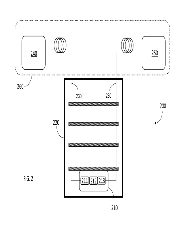
[00029] FIG. 2 shows an example embodiment of a system which
uses a photonics-based
system to control or measure an array of solid-state qubits;
[00030] FIG. 3 shows an example embodiment of a system which
uses multiplexing to
control or measure an array of solid-state qubits using a single optical fiber
link;
[00031] FIG. 4 shows an example embodiment of a system which
uses modulation of opti-
cal frequency combs as a multiplexing method to control or measure an array of
solid-state
qubits using a single optical fiber link;
[00032] FIG. 5 shows an example embodiment of a system which
uses an optical arbitrary
wave generator to achieve multiplexing to control or measure an array of solid-
state qubits using
a single optical fiber link;
[00033] FIG. 6 shows an example of a system which uses an
amplifier to amplify the input
control or readout signal after it has been converted from optical frequencies
to microwave fre-
quencies.
[00034] FIG. 7 shows an example of a system which uses a single
coaxial cable to supply
a microwave pump signal to an array of amplifiers.
[00035] FIG. 8 shows an example of a quantum processor in which
optical circuitry and
qubits are integrated on the same substrate; and
[00036] FIG. 9 shows an example of a multi-chip quantum
processor in which qubits are
fabricated on one substrate and optical circuitry is fabricated on a second
substrate.
DETAILED DESCRIPTION
[00037] The present disclosure is directed to a scalable solid-
state quantum computing
platform where the quantum processor is operated at ultra-low temperatures and
the need to use
CA 03201105 2023- 6-2
WO 2022/120469
PCT/CA2021/051748
a significant number of coaxial cables is alleviated. The connection between
the quantum
processor and the quantum control system is achieved using optical fibers, and
sending control
or readout pulses to the solid state quantum processor operated at ultra-low
temperatures uses a
photonics approach.
[00038] FIG. 1 shows an example embodiment of a solid-state
quantum computing system
100 in accordance with the prior art. The system 100 comprises a quantum
processor 110 placed
inside a cryogenics apparatus 120 such as a dilution fridge, and cooled down
to ultra-low
temperatures. Control and readout of the qubits in the quantum processor 110
is performed by a
quantum control system 160. The quantum control system 160 may itself have
separate modules
for uplink and downlink. As used herein, any signal originating from the
quantum control system
160 and delivered to the quantum processor 110, either for qubit control or
readout, is referred to
as "uplink" and any signal originating from the quantum processor 110 and
delivered to the
quantum control system 160 is referred to as "downlink". In FIG. 1, an uplink
module 140
generates the necessary microwave pulses for qubit control and readout. The
microwave pulses
are transmitted to the quantum processor 110 via a set of coaxial lines 170A
that are thermally
anchored to cold stages 121 of the cryogenic apparatus 120 through a set of
attenuators 122.
Qubit states are measured through a set of coaxial lines 170B that leave the
quantum processor
110 and connect to the downlink module 150 which is at room temperature and
outside the
cryogenics apparatus 120. The set of coaxial lines 170B are also thermally
anchored to the cold
stages 121 of the cryogenics apparatus 120 through the set of attenuators 122.
This qubit
readout chain may also involve one or more amplifiers 180 and/or circulators
190 to further
improve the signal to noise ratio and protect the qubits from microwave
feedback.
[00039] The quantum processor 110 requires at least one control
coaxial line per qubit on
top of a number of readout coaxial lines. Additional coaxial lines can also be
required to control
couplers used to implement multi-qubit gates. These coaxial lines are bulky,
expensive, and also
result in heat leak from the hotter stages of the cryogenics apparatus 120 to
the colder areas.
6
CA 03201105 2023- 6-2
WO 2022/120469
PCT/CA2021/051748
Noting that the cooling power of the cryogenics apparatus 120 decreases with
temperature,
installing more than a few hundred coaxial lines is challenging as the heat
leak from the coaxial
lines may exceed the cooling power of the cryogenics apparatus 120.
[00040] Moreover, practical applications of quantum computers
typically require hundreds
of thousands, and even millions, of qubits. Therefore, the solid-state quantum
computing system
100 in accordance with the prior art is not scalable for large scale quantum
processors. The
present disclosure addresses these shortcomings by making use of optical
fibers, which result in
significantly lower heat load compared to coaxial cables. Optical fibers also
provide large
bandwidth which allows the use of multiplexing to address a large number of
qubits with a single
fiber.
[00041] FIG. 2 illustrates an example quantum computing system
200 in accordance with
the present disclosure. The system 200 comprises a quantum processor 210 which
is housed
inside a cryogenics apparatus 220 such as a dilution fridge. The quantum
processor 210
comprises one or more optical-to-microwave converters 211 which down-convert
optical signals
to microwave signals. The microwave signals are delivered to one or more
quantum circuit
elements 212 such as solid-state qubits and couplers operating in a sub-Tera
Hertz frequency
band. Microwave signals originating from quantum circuit elements 212 are up-
converted to
optical frequencies by one or more microwave-to-optical converters 213. The
quantum processor
210 is connected to a quantum control system 260 through one or more fiber
optic links 230.
The quantum control system 260 may itself have separate subsystems for uplink,
such as uplink
module 240, and downlink, such as downlink module 250. In some embodiments,
the quantum
control system 260 comprises one integrated system for uplink and downlink. In
some other
embodiments, the quantum control system 260 comprises physically separate
subsystems for
uplink and downlink.
[00042] Optical-to-microwave converters 211 may for example
consist of photodiodes,
such as InGaAs photodiodes, or single-photon detectors. Microwave-to-optical
converters 213
7
CA 03201105 2023- 6-2
WO 2022/120469
PCT/CA2021/051748
may for example consist of optical phase modulators, such as LiNb03-based
electro-optical
phase modulators, or other transducers based on optomechanics, piezo-
optomechanics, electro-
optics or magneto-optics.
[00043] In some embodiments, parts or all of the quantum control
system 260 and/or its
subsystems may reside inside the cryogenics apparatus 220.
[00044] Instead of pulse shaping microwave signals and
delivering them to a quantum
processor through coaxial cables, the quantum control system 260 modulates and
demodulates
optical signals that are delivered to or originate from the quantum processor
210 through optical
fibers 230. The optical signals may have a wavelength in the short-wave
infrared band, for which
the transmission of optical fibers is maximal.
[00045] In some embodiments, one or more multiplexing schemes,
such as Wavelength-
Division Multiplexing (WDM), may be used to control and/or measure multiple
qubits at the same
time. FIG. 3 illustrates an example embodiment of the uplink side of a quantum
computing
system 300 implementing a multiplexing scheme. In this example, an uplink
module 340
comprises an array of optical sources 341 followed by an array of modulators
342 before the
optical signals are combined using a multiplexer into an optical fiber 330 and
multiplexed optical
signals are delivered to a quantum processor 310 located inside a cryogenics
apparatus 320.
[00046] FIG. 4 illustrates another example of the uplink side of
a quantum computing
system 400 where an uplink module 440 uses a frequency comb source 441 rather
than an array
of optical sources. In one example implementation, the frequency comb source
441 may
comprise a mode-locked laser which is self-referenced. In another example
implementation, the
frequency comb source 441 may rely on strong electro-optic phase modulation of
a continuous
laser to generate the frequency comb. In yet another example implementation,
the frequency
comb source 441 may comprise a light source such as a continuous laser
connected to a
nonlinear (Kerr) micro-resonator which creates a frequency comb through
nonlinear mixing. In all
8
CA 03201105 2023- 6-2
WO 2022/120469
PCT/CA2021/051748
of these examples, multiplexed optical signals are used to address multiple
qubits, whereby
signals of different frequencies are used to address different qubits.
[00047]
In one implementation, the frequency comb generated by the source 441 may
pass through a demultiplexer 442 which separates the comb lines and routes
them to individual
modulators 443 (e.g. a Mach-Zehnder modulator) for pulse shaping. Each
frequency line in the
frequency comb may be intended for preforming an operation on an individual
quantum circuit
element (e.g. a qubit or a coupler) located in a quantum processor 410. The
individual
modulators 443 are used to provide pulse shaping on individual frequencies
according to the
particular operation intended to be performed on a respective quantum circuit
element in the
quantum processor 410. The channels are then recombined by a multiplexer 444
before
transmission over an optical fiber 430 to the quantum processor 410 located
inside a cryogenics
apparatus 420.
[00048]
FIG. 5 illustrates another example embodiment of the uplink side of a
quantum
computing system 500 in which an uplink module 540 comprises a frequency comb
source 541
and an optical arbitrary wave generator (OAWG) 542, such as a line-by-line
pulse shaper, which
translates quantum operations to waveforms. The multiplexed optical signal
output by the
generator 542 is delivered via an optical fiber 530 to a quantum processor 510
located inside a
cryogenics apparatus 520.
[00049]
Fig. 6 illustrates another example embodiment of the uplink side of a
quantum
computing system 600 which allows the use of a lower optical power in an
uplink module 640 and
optical fibers 630 to avoid excessive heating in a quantum processor 610
located inside a
cryogenics apparatus 620. Since the passive heat load (i.e. due to heat
propagating along the
fiber) of optical fibers is negligible, what may limit the scalability of
optically controlled quantum
computers is the active heat load, i.e. heat due to the dissipation of the
optical power at the exit
of the optical fiber. The quantum processor 610 comprises a microwave
amplifier 614 between
an optical-to-microwave converter 611 and quantum circuit elements 612. In
some embodiments,
9
CA 03201105 2023- 6-2
WO 2022/120469
PCT/CA2021/051748
the microwave amplifier 614 can be a quantum-limited parametric amplifier,
such as a Josephson
Parametric Amplifier (JPA) or a Travelling-Wave Parametric Amplifier (TWPA),
which are
designed not to introduce any additional noise.
[00050] Fig. 7 illustrates a system 700 having a plurality of
optical fibers 730 and a plurality
of optical-to-microwave converters 711A, 711B, 711C. The microwave signal
generated by each
optical-to-microwave converter 711A, 711B, 711C is amplified by a respective
amplifier 714A,
714B, 714C before being directed to quantum circuit elements 712 of a quantum
processor 710
located inside a cryogenic apparatus 720. To minimize the number of coaxial
cables in the
cryogenic apparatus 720, a single coaxial cable 750 can be used to supply a
microwave pump
signal to the amplifiers 714A, 714B, 714C. In Fig. 7, an uplink module 740
provides both control
optical signals and the microwave pump signal, but these signals could also be
provided by
different and separate modules. Alternatively, with an all-optical quantum
control system, the
microwave pump signal could also be generated from an optical signal provided
by optical fibers
and down converted to microwave frequencies by an optical-to-microwave
converter.
[00051] FIG. 8 depicts a quantum processor 800 according to one
embodiment. The
quantum processor 800 comprises at least one substrate 810. Solid-state
quantum circuit
elements, such as qubits and couplers, are fabricated on the substrate through
a series of
nanofabrication techniques such as lithography, deposition, etching, and lift
off. In one example
embodiment, these quantum circuit elements are fabricated on one side of the
substrate as part
of layer 820. The quantum processor 800 also comprises microwave circuit
elements, such as
readout resonators, microwave filters and transmission lines, which may also
be fabricated on
the substrate 810 through a series of nanofabrication techniques such as
lithography, deposition,
etching, and lift off. The microwave circuit elements may be fabricated on
either side of the
substrate 810 and/or as part of layer 820. The quantum processor 800 may also
include another
set of integrated photonic element such as waveguides, ring resonators, and
optical-to-
microwave converters. These photonics elements may be fabricated in layer 830,
on the same
CA 03201105 2023- 6-2
WO 2022/120469
PCT/CA2021/051748
side of the substrate as the quantum circuit elements, and/or on the opposite
side of the
substrate in layer 840. In the case where there are elements on both sides of
the substrate, the
electrical connection between both sides of the substrate may be achieved
using vias 850. The
integrated photonics circuitry may be connected to a single or an array of
optical fibers 860A,
860B for data transmission.
[00052] FIG. 9 depicts a quantum processor 900 according to
another embodiment. The
quantum processor comprises at least one multi-chip module (MCM) 970. In this
arrangement,
quantum circuit elements may be fabricated in layer 940 on a first substrate
910 while another
substrate 920 carries another segment of circuitry and elements such as
photonic elements in
layer 960. Microwave circuit elements may reside on either substrate 910, 920,
in layer 940
and/or layer 950. Elements fabricated on different substrates in layer 940 and
layer 950 are
electrically connected through a plurality of bond bumps 930, such as
superconducting bond
bumps. The multi-chip module 970 can also include additional substrates, for
example a third
substrate hosting one or a plurality of amplifiers (not shown). Amplifiers may
also be fabricated
on substrate 920, on either side thereof. It will be understood that other
variants of 3D integration
of such multi-chip quantum processors are possible, including but not limited
to multi-chip vertical
stack, flip-chip, and die on wafer arrangements.
[00053] The above description is meant to be exemplary only, and
one skilled in the art will
recognize that changes may be made to the embodiments described without
departing from the
scope of the disclosure. Still other modifications which fall within the scope
of the present disclo-
sure will be apparent to those skilled in the art, in light of a review of
this disclosure.
[00054] Various aspects of described herein may be used alone,
in combination, or in a
variety of arrangements not specifically discussed in the embodiments
described in the foregoing
and is therefore not limited in its application to the details and arrangement
of components set
forth in the foregoing description or illustrated in the drawings. For
example, aspects described in
one embodiment may be combined in any manner with aspects described in other
embodiments.
11
CA 03201105 2023- 6-2
WO 2022/120469
PCT/CA2021/051748
The scope of the following claims should not be limited by the embodiments set
forth in the ex-
amples, but should be given the broadest reasonable interpretation consistent
with the descrip-
tion as a whole.
12
CA 03201105 2023- 6-2