Note: Descriptions are shown in the official language in which they were submitted.
WO 2022/130184
PCT/1B2021/061667
PHOTOIONIZATION DETECTOR AND METHOD OF OPERATING SAME
RELATED APPLICATIONS
[0001] This application claims priority to United States
Provisional Application No.
63/124,892 filed December 14, 2020, which is incorporated herein by reference.
FIELD OF THE DISCLOSURE
[0002] This disclosure relates to a photoionization detector for
the detection of gas or
vapor molecules with photoionization technology and the general operation of
such a
photoionization detector. More specifically, this disclosure provides a
configuration and
approach to minimize the impact of environment humidity and to increase the
photoionization detector reliability for both indoor and outdoor applications.
DESCRIPTION OF RELATED ART
[0003] The concern for clean living, working and the industrial
environment has increased
over the recent decades. Various methods and instruments have been developed
to address
these concerns through accurate measurement of contaminations or pollution
concentration,
especially for gas contaminations. Volatile organic compounds (VOCs) remain
challenging
because of the colorlessness, low odor, and high reduction-oxidation reaction
(as known as
redox) potential in general. Photoionization detectors ("PIDs") are one of the
successful
solutions to tackle this difficulty because they use high energy photons to
break the VOC
molecules into ions and free electrons (thereby generating a plasma) and
accurately
measuring the plasma current which typically correlates to the VOC
concentration. The
measurement range is typically 0.01-10,000 parts per million (ppm), as
compared to the
measurement range of other devices, e.g., 0.5-50,000 ppm for flame ionization
detectors
("FIDs"), 100-50,000 ppm for infrared (IR) analyzers, 1-10,000 ppm for metal
oxide
semiconductors ("MOS"), and 200-50,000 ppm for catalytic oxidation bead
combustible gas
(LEL) sensors.
[0004] The general working principle of PIDs is the measurement of
ionic current which
is related to the gas concentration when the gas molecules are ionized by high
energy
ultraviolet (UV) light. The electrons are moved into an electrical field
between two
electrodes and are collected on the positive electrode to form a current which
is generally
proportional to the gas concentration. One key part of the PID is the lamp
which is usually
1
CA 03202094 2023- 6- 13
WO 2022/130184
PCT/1B2021/061667
filled with a low-pressure inert gas that emits photons in the vacuum-
ultraviolet region. Salt
crystals (e.g., MgF2, LiF, CaF2, BaF2) are used as windows because common
silica glasses do
not transmit the short wavelength light required to ionize target VOCs.
Examples of inert fill
gases are Ar, Ke, H2, or Xe. Another key part of the PID is the electrodes,
which collect the
plasma/ionic current in a high voltage electric field (applied on both the
counter and sensing
electrodes). Usually, the electrons are collected by the sensing electrode
(anode, positively
charged) and the resultant cations are collected by the counter electrode
(cathode, negatively
charged).
[0005] Ideally, the current from the sensing electrode is
proportional to the gas
concentration. However, in the field, the surrounding temperature and humidity
of the PID
varies, which might result in a formation of condensation or mist outside or
even inside of the
PID. This condensation might lead to a false reading and misinterpretation of
the current
VOC level. The false reading might come from a leak current between the
counter electrode
and the sensing electrode, which is due to the formation of a conducting path
as a result of
condensation and other possibilities. Thus, the design to overcome such
challenges like
condensation or mist is critical for a robust PID. One method toward
overcoming this issue is
to use filters, but such method has generally proven to be difficult to
implement and/or is not
achieving the desired performance.
[0006] Another method, which has had general success in the
marketplace, and developed
by Ion Science Limited, is to use another electrode, for example, a fence
electrode, that is
generally disposed within an ionization chamber between the sensing electrode
and the
counter electrode to "block" the leak current from reaching the sensing
electrode, thus
essentially making the leak current zero or close to zero. This method is
generally described
and illustrated in United States Patent No. 7,046,012. More specifically, as
described in
United States Patent No. 7,046,012, the sensing electrode is positioned at one
end of the
ionization chamber proximate to the lamp window while the counter electrode is
positioned
at an opposite end of the ionization chamber, distal from the lamp window, and
the fence
electrode is positioned within the ionization chamber between the sensing
electrode and the
counter electrode. In practice, electrical potential is applied to each of the
electrodes with the
electrical potential applied to the fence electrode being equal to, or
substantially equal to, the
electrical potential applied to the sensing electrode, with such electrical
potential being
different from the electrical potential applied to the counter electrode, such
that a voltage
differential is defined between the sensing electrode and the counter
electrode. With the
2
CA 03202094 2023- 6- 13
WO 2022/130184
PCT/1B2021/061667
electrical potentials applied, the current from the counter electrode to the
sensing electrode is
measured, which is essentially equal to the plasma/ionic current.
[0007] The foregoing method, however, has some disadvantages. More
specifically, the
foregoing method only "blocks" the leak current within the ionization chamber.
However,
based on testing, it has been determined that a larger percentage of the leak
current occurs
outside of the ionization chamber, namely on a surface of the sub strate(s)
(that forms the
ionization chamber) that faces the gas inlet.
[0008] As a result of the foregoing, certain individuals would
appreciate further
improvements in PIDs and the operation of same.
BRIEF SUMMARY
[0009] Accordingly, the present disclosure provides an electrode
stack assembly includes
an electrically insulative substrate having a cavity therethrough extending, a
first counter
electrode on a top surface thereof and extending through the substrate, a
second sensing
electrode on a bottom surface thereof and extending through the substrate, and
a third
electrode having a top body portion on a top of the substrate, a bottom body
portion on a
bottom of the substrate, and a coupling pin passing through the substrate and
electrically
coupling the top and bottom body portions. The third electrode electrically
separates the pin
of the sensing electrode from the counter electrode. In a first embodiment,
the top body
portion encircles the pin of the pin of the sensing electrode, and is spaced
therefrom, and the
bottom body portion encircles the body of the sensing electrode, and is spaced
therefrom. In
a second embodiment, the top body portion encircles the body of the counter
electrode, and is
spaced therefrom, and the bottom body portion encircles the pin of the sensing
electrode, and
is spaced therefrom. In a third embodiment, the top body portion encircles the
pin of the
sensing electrode, and is spaced therefrom, and the bottom body portion
encircles the pin of
the counter electrode, and is spaced therefrom.
[0010] A method of operating a photoionization detector is also
provided. In a first
embodiment of the method, the following is provided: applying a first electric
potential to a
counter electrode on a top surface of an electrically insulative substrate,
applying a second
electric potential to a sensing electrode on a bottom surface of the
insulative substrate,
applying a third electric potential to an electrode having a top body portion
on the top surface
of the substrate and a bottom body portion on the bottom surface of the
substrate, the top and
bottom body portions being electrically coupled together, and the top and
bottom body
3
CA 03202094 2023- 6- 13
WO 2022/130184
PCT/1B2021/061667
portions separating a current path of the counter electrode from a current
path of the sensing
electrode, wherein the first and third electric potentials are the same or
generally the same,
and the second electric potential is generally higher than the first
potential, and ionizing gas
in a cavity of the insulative substrate. In a second embodiment of the method,
the following
is provided: applying a first electric potential to a counter electrode on a
top surface of an
electrically insulative substrate, applying a second electric potential to a
sensing electrode on
a bottom surface of the insulative substrate, applying a third electric
potential to an electrode
having a top body portion on the top surface of the substrate and a bottom
body portion on
the bottom surface of the substrate, the top and bottom body portions being
electrically
coupled together, and the top and bottom body portions separating a current
path of the
counter electrode from a current path of the sensing electrode, wherein the
second and third
electric potentials are the same or generally the same, and the second
electric potential is
generally higher than the first potential, and ionizing gas in a cavity of the
insulative
substrate.
BRIEF DESCRIPTION OF THE DRAWINGS
[0011] The present disclosure is illustrated by way of example, and
not limited, in the
accompanying figures in which like reference numerals indicate similar
elements and in
which:
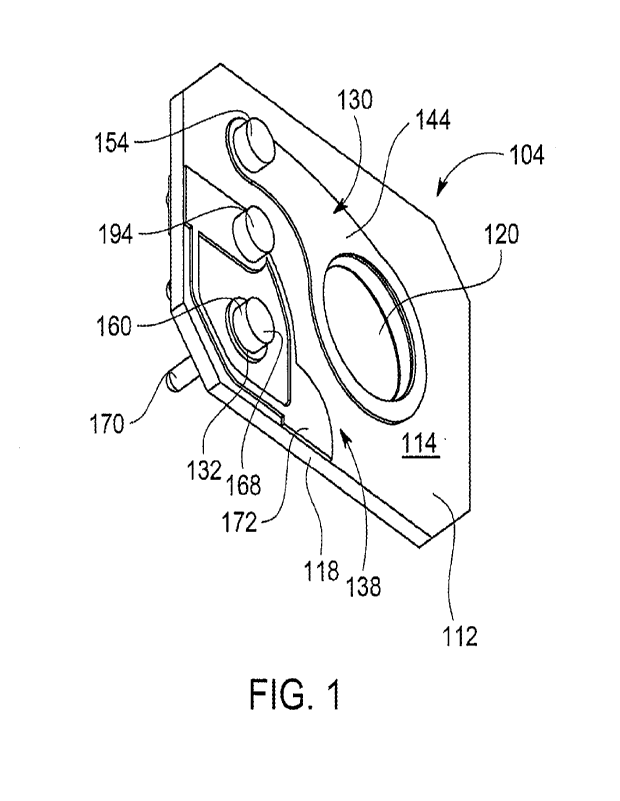
[0012] FIG. 1 depicts a top perspective view of an electrode stack
assembly according to a
first embodiment;
[0013] FIG. 2 depicts a bottom perspective view of the electrode
stack assembly;
[0014] FIG. 3 depicts a top plan view of the electrode stack
assembly;
[0015] FIG. 4 depicts a bottom plan view of the electrode stack
assembly;
[0016] FIG. 5 depicts an exploded perspective view of the electrode
stack assembly;
[0017] FIG. 6 depicts a cross-sectional view of a photoionization
detector including the
electrode stack assembly of FIG. 1;
[0018] FIG. 7 depicts a top perspective view of an electrode stack
assembly according to a
second embodiment;
[0019] FIG. 8 depicts a bottom perspective view of the electrode
stack assembly of FIG.
7;
[0020] FIG. 9 depicts a top plan view of the electrode stack
assembly of FIG. 7;
[0021] FIG. 10 depicts a bottom plan view of the electrode stack
assembly of FIG. 7;
4
CA 03202094 2023- 6- 13
WO 2022/130184
PCT/1B2021/061667
[0022] FIG. 11 depicts an exploded perspective view of the
electrode stack assembly of
FIG. 7;
[0023] FIG. 12 depicts a cross-sectional view of a photoionization
detector including the
electrode stack assembly of FIG. 7;
[0024] FIG. 13 depicts a top perspective view of an electrode stack
assembly according to
a second embodiment;
[0025] FIG. 14 depicts a bottom perspective view of the electrode
stack assembly of FIG.
13;
[0026] FIG. 15 depicts atop plan view of the electrode stack
assembly of FIG. 13;
[0027] FIG. 16 depicts a bottom plan view of the electrode stack
assembly of FIG. 13;
[0028] FIG 17 depicts an exploded perspective view of the electrode
stack assembly of
FIG. 13; and
[0029] FIG. 18 depicts a cross-sectional view of a photoionization
detector including the
electrode stack assembly of FIG. 13.
DETAILED DESCRIPTION
[0030] While the disclosure may be susceptible to embodiment in
different forms, there is
shown in the drawings, and herein will be described in detail, specific
embodiments with the
understanding that the present disclosure is to be considered an
exemplification of the
principles of the disclosure, and is not intended to limit the disclosure to
that as illustrated
and described herein. Therefore, unless otherwise noted, features disclosed
herein may be
combined to form additional combinations that were not otherwise shown for
purposes of
brevity. It will be further appreciated that in some embodiments, one or more
elements
illustrated by way of example in a drawing(s) may be eliminated and/or
substituted with
alternative elements within the scope of the disclosure.
[0031] Contrary to the prior art PIDs and operation methods used as
described above, the
current disclosure handles the issue with alternative configurations and
methods, which
alternative configurations and methods not only provide a plasma/ionic
current, but also
provides further advantages as will be explained in further detail
hereinbelow. In the PIDs of
the designs described in detail below, and the associated methods of use: (1)
an electrode is
partially located around the sensing electrode (which is understood to be the
primary pathway
of surface leak current), but not located in/around the ionization chamber;
(2) an air-gapped
multi-layer electrode structure may be provided which assists in preventing
the leak current
CA 03202094 2023- 6- 13
WO 2022/130184
PCT/1B2021/061667
leaking across layers instead of using a metallic layer to "block" the leak
current; and (3) the
surface of metal layer is not coated with dielectric material.
[0032] The leak current between the counter electrode and the
sensing electrode has
several possibly pathways in the electrode structure: (1) between electrode
layers (if electrode
contains multiple layers); (2) on the surface of the same electrode layer;
and/or (3) on the
edge of the same layer. There are also two general methods to alleviate the
impact of the leak
current, either to block or measure the leak current. Both methods rely on
rational designs on
the leak current pathways to either stop or collect the leak current. Herein,
a design/method
uses a combined with spaced electrode layers to limit the leak current within
the same
electrode layer to block/compensate the leak current and afford a humidity
resistant PID
electrode.
[0033] The leak current on the electrode surface will be stopped or
collected by a
guard/auxiliary electrode to reduce/compensate the impact of the humidity-
introduced leak
current. There are three major considerations for this design. (1) the
humidity reaches the
surfaces of electrode layers and build a condensation water trace on surfaces,
which will
provide a conductive pathway once enough ions are dissolved into this water
trace, (2) the
counter electrode and the sensing electrode have the longest edge on the outer
side of the
counter electrode or the sensing electrode, which yields the highest
possibility of building a
conductive path; and (3) the guard/auxiliary electrode encircles the counter
electrode/sensing
electrode and has a potential equal or close to the sensing electrode (block
mode) or to the
counter electrode (compensation mode) which helps assure an effective
reduction/compensation of the leak current. The design described herein also
provides for the
counter electrode to be on one side of a substrate, and the sensing electrode
on the other side
of the substrate, which greatly simplifies the production process and makes
the design cost-
effective and mass reproducible.
[0034] Additional designs/methods may be used to prevent the leak
current, if two or
more layers of substrates (on which the electrode are attached) are used. For
instance,
substrates may be configured to contact each other only with pins/other
mechanical structures
to create an air gap in the ionization chamber between layers and minimize the
leak current
across two layers. With the air-gapped electrode substrate, the leak current
will be limited
within the same electrode substrate layer and not travel to the other
electrode substrate layer.
In addition, pin mounting holes are designed to be slightly larger than the
diameter of the pins
6
CA 03202094 2023- 6- 13
WO 2022/130184
PCT/1B2021/061667
to create a small air gap between each pin and the electrode substrate to
minimize the current
leaking on the supporting substrate.
[00351 The guard/auxiliary electrode encircles around the counter
electrode or the sensing
electrode on the same side of the sensing electrode and the counter electrode.
The potential
of the guard/auxiliary electrode will be held at or close to the potential of
the sensing
electrode (block mode) or the counter electrode (compensation mode). Multiple
guard/auxiliary electrodes/pins may be provided on one surface. In the block
mode, the leak
current is stopped by the electrode functioning as a guard electrode, and the
measured current
is considered as the true plasma current, which correlates to the gas
concentration. In the
compensation mode, the leak current is subtracted from the total current to
afford the true
plasma current_ The guard/auxiliary electrode is not provided in the inner
surface of the
electrode layers (e.g., in/around the ionization chamber) since the leak
current from these two
surfaces is minimal (potential is only applied around the mounting pins).
[0036] A first embodiment of a photoionization detector ("PID") 100
is shown in FIGS. 1-
6. A second embodiment of a photoionization detector ("PID") 200 is shown in
FIGS. 7-12.
A third embodiment of a photoionization detector ("PID") 300 is shown in FIGS.
13-18.
[0037] Attention is directed to FIGS. 1-6 and the first embodiment
of the PID 100. PID
100 includes a lamp assembly 102 and an electrode stack assembly 104 which are
operatively
associated with one another. The PID 100 and the electrode stack assembly 104
are intended
to be operated in the block mode or the compensation mode.
[0038] As illustrated in FIG. 6, the lamp assembly 102 includes a
light chamber 106
defined by one or more walls 108. A window 110 is provided at an end of the
walls 108
(illustrated in FIG. 6 as being at a top end of the walls 108). The walls 108
are preferably
formed of glass and the window 110 is preferably formed of salt crystals
(e.g., MgF2, LiF,
CaF2, BaF2) as they allow for the transmission of the vacuum UV light required
to ionize
target compounds. The light chamber 106 may contain a low-pressure inert gas
such as Ar,
Ke, Hz, or Xe, as is known to those skilled in the art.
[00391 The electrode stack assembly 104 includes a substrate 112
that is preferably
formed of a waterproof/water repellant, electrically insulative material, such
as that
commonly sold under the trademark TEFLON. The substrate 112 has a top surface
114, a
bottom surface 116 and one or more outer surfaces 118 which connect the top
surface 114 to
the bottom surface 116. The one or more outer surfaces 118 extend in a first
direction (for
example along a z-axis). The substrate 112 has a cavity 120 provided
therethrough from the
7
CA 03202094 2023- 6- 13
WO 2022/130184
PCT/1B2021/061667
top surface 114 to the bottom surface 116. The cavity 120 functions as an
ionization gas
chamber (as will be discussed in further detail hereinbelow) that is defined
by one or more
walls 122 (depicted in the drawings as a single, circular-shaped wall which
extends in the
first direction). It should be noted that while the cavity 120 is illustrated
as a single hole, that
the cavity 120 could alternatively be configured as a plurality of separate
holes (formed in a
pattern or randomly). As shown in FIG. 5, the substrate 112 has three pin
mounting holes
124, 126, 128 provided therethrough from the top surface 114 to the bottom
surface 116. The
pin mounting holes 124, 126, 128 are defined by one or more walls. The centers
of the pin
mounting holes 124, 126, 128 may be in alignment with each other in a second
direction
which is perpendicular to the first direction (for example along a y-axis) and
the center of the
pin mounting hole 126 and the center of the cavity 120 may be in alignment
with each other
in a third direction perpendicular to the first and second directions (for
example along an x-
axis). While a single substrate 112 is shown in the drawings, it is to be
understood that
multiple substrates could be provided that have common configurations, where
the substrates
are separated from one another and those portions identified as being
associated with the top
surface of the substrate are associated with the top surface of an top
substrate and those
portions identified as being associated with the bottom surface of the
substrate are associated
with the bottom surface of a bottom substrate.
[0040] The electrode stack assembly 104 includes a first electrode
130 which forms a
counter electrode, an optional top contact pad 132, a second electrode 134
which forms a
sensing electrode, an optional bottom contact pad 136, and a third electrode
138 which in one
mode provides a guard electrode and another mode provides an auxiliary
electrode.
[0041] As best illustrated in FIGS. 1 and 3, the top contact pad
132 (if provided) is
provided on the top surface 114 of the substrate 112 and has a pin mounting
hole 140
provided therethrough. The bottom surface of the top contact pad 132 (if
provided) is further
positioned on the top surface 114 of the substrate 112 such that the pin
mounting hole 140 is
in alignment with the pin mounting hole 128 through the substrate 112. The
diameter of the
pin mounting hole 140 is sized to generally match the diameter of the pin
mounting hole 128.
[0042] As best illustrated in FIGS. 2 and 4, the bottom contact pad
136 (if provided) is
provided on the bottom surface 116 of the substrate 112 and has a pin mounting
hole 142
provided therethrough. The top surface of the bottom contact pad 136 is
further positioned
on the bottom surface 116 of the substrate 112 such that the pin mounting hole
142 of the
bottom contact pad 136 is in alignment with the pin mounting hole 124 through
the substrate
8
CA 03202094 2023- 6- 13
WO 2022/130184
PCT/1B2021/061667
112. The diameter of the pin mounting hole 142 of the bottom contact pad 136
is sized to
generally match the diameter of the pin mounting hole 124.
[00431 As best illustrated in FIGS. 1 and 3, the counter electrode
130 is provided on the
top surface 114 of the substrate 112. The counter electrode 130 includes a
body 144 and a
pin 146 extending therefrom. The body 144 has a top surface, a bottom surface
and a
continuous outer edge 148 extending between the top and bottom surfaces. An
opening 150
and a pin mounting hole 152 are provided through the body 144, are spaced from
each other
and are spaced from the outer edge 148, and extend from the top surface to the
bottom
surface.
[00441 The bottom surface of the counter electrode 130 is
positioned on the top surface
114 of the substrate 112 such that the opening 150 is in alignment with the
cavity 120
through the substrate 112, and such that the pin mounting hole 152 is in
alignment with the
pin mounting hole 124 through the substrate 112. The diameter of the opening
150 is sized to
generally match the diameter of the cavity 120, and the diameter of the pin
mounting hole
152 is sized to generally match the diameter of the pin mounting hole 124. The
pin 146 has
an enlarged head portion 154 that preferably has an outer diameter that is
larger than a
diameter of the pin mounting hole 124, and an elongated shaft 156 extending
therefrom. The
enlarged head portion 154 of the pin 146 rests on the top surface of the body
144, and the
shaft 156 extends through the pin mounting hole 152 of the body 144, through
the pin
mounting hole 124 of the substrate 112, through the pin mounting hole 142 of
the bottom
contact pad 136 (if provided), and extends from the bottom surface of the
counter electrode
130. The pin 146 is preferably held in place by known means, e.g., soldering
to the body 144
and, to the bottom contact pad 136 (if provided). While the body 144 and the
pin 146 are
described as two separate components permanently mated together, in an
embodiment, the
body 144 and the pin 146 are integrally formed as one piece.
[00451 As best illustrated in FIGS. 1 and 3, the sensing electrode
134 is provided on the
bottom surface 116 of the substrate 112. The sensing electrode 134 includes a
body 158 and
a pin 160 extending therefrom. The body 158 has a top surface, a bottom
surface and a
continuous outer edge 162 extending between the top and bottom surfaces. An
opening 164
and a pin mounting hole 166 are provided through the body 158, are spaced from
each other
and are spaced from the outer edge 162, and extend from the top surface to the
bottom
surface.
9
CA 03202094 2023- 6- 13
WO 2022/130184
PCT/1B2021/061667
[0046] The top surface of the sensing electrode 134 is positioned
on the bottom surface
116 of the substrate 112 such that the opening 164 is in alignment with the
cavity 120
through the substrate 112 and such that the pin mounting hole 166 is in
alignment with the
pin mounting hole 128 through the substrate 112. The diameter of the opening
164 is sized to
generally match the diameter of the cavity 120, and the diameter of the pin
mounting hole
166 is sized to generally match the diameter of the pin mounting hole 128. The
pin 160 has
an enlarged head portion 168 that preferably has an outer diameter that is
larger than a
diameter of the pin mounting hole 128, and an elongated shaft 170 extending
therefrom. The
enlarged head portion 168 of the pin 160 rests on the top surface of the top
contact pad 132
(if provided; if the top contact pad 132 is not provided then the head portion
168 rests on the
top surface 114 of the substrate 112), and the shaft 170 extends through the
top contact pad
132 (if provided), through the pin mounting hole 128 of the substrate 112,
through the pin
mounting hole 166 of the body 158, and extends from the bottom surface of the
body 158.
The pin 160 is preferably held in place by known means, e.g., soldering to the
body 158 and,
to the top contact pad 132 (if provided). While the body 158 and the pin 160
are described as
two separate components permanently mated together, in an embodiment, the body
158 and
the pin 160 are integrally formed as one piece.
[0047] The third electrode 138 includes a top body portion 172, a
bottom body portion
174 which are coupled together by a coupling pin 176.
[0048] The top body portion 172 has a top surface, a bottom surface
and a continuous
outer edge 178 extending between the top and bottom surfaces. An opening 180
formed by a
continuous wall 182 and a pin mounting hole 184 are provided through the top
body portion
172, are spaced from each other and are spaced from the outer edge 178, and
extend from the
top surface to the bottom surface. The bottom surface of the top body portion
172 is provided
on the top surface 114 of the substrate 112 such that the pin mounting hole
184 is in
alignment with the pin mounting hole 126 through the substrate 112. The top
contact pad
132 (if provided) and the enlarged head portion 168 of the pin 160 are
encircled within, but
separated from, the wall 182. The pin mounting hole 184 is sized to generally
match the
diameter of the pin mounting hole 126.
[0049] The bottom body portion 174 has a top surface, a bottom
surface and a continuous
outer edge 186 extending between the top and bottom surfaces. An opening 188
formed by a
continuous wall 190 and a pin mounting hole 192 are provided through the
bottom body
portion 174, are spaced from each other and are spaced from the outer edge
186, and extend
CA 03202094 2023- 6- 13
WO 2022/130184
PCT/1B2021/061667
from the top surface to the bottom surface. The top surface of the bottom body
portion 174 is
provided on the bottom surface 116 of the substrate 112 such that the pin
mounting hole 192
is in alignment with the pin mounting hole 126 through the substrate 112. The
sensing
electrode 134 is encircled within, but separated from, the wall 190. The
diameter of the pin
mounting hole 192 is sized to generally match the diameter of the pin mounting
hole 126.
[0050] The coupling pin 176 has an enlarged head portion 194 that
preferably has an outer
diameter that is larger than a diameter of the pin mounting hole 126, and an
elongated shaft
196 extending therefrom. The enlarged head portion 194 of the coupling pin 176
rests on the
top surface of the top body portion 172, and the shaft 196 extends through the
pin mounting
hole 184 of the top body portion 172, through the pin mounting hole 126 of the
substrate 112,
through the pin mounting hole 192 of the bottom body portion 174, and the
shaft 196 extends
from the bottom surface of the bottom body portion 174. Coupling pin 176 is
preferably held
in place by known means, e.g., soldering to the top body portion 172 and to
the bottom body
portion 174.
[0051] The enlarged head portion 154, 168, 194 of each pin 146,
160, 176 preferably has
an outer diameter that is larger than a diameter of the pin mounting hole 124,
128, 126. The
elongated shafts 156, 170 of pins 146, 160 preferably has an outer diameter
that is smaller
than the diameter of the pin mounting hole 124, 128 to create a small air gap
between each
pin 146, 160 and the substrate 112 to minimize the current leaking on the
substrate 112. The
elongated shaft 196 of the pin 176 may have an outer diameter that is
substantially the same
as the diameter of the pin mounting hole 126.
[0052] In use, an electric potential is applied from below the
substrate 112 to the pin 146
which applies electric potential to the body 144 of the counter electrode 130
and to the
bottom contact pad 136 (if provided), an electric potential is applied from
below the substrate
112 to the pin 160 which applies electric potential to the body 158 of the
sensing electrode
134 and to the top contact pad 132 (if provided), and an electric potential is
applied from
below the substrate 112 to the coupling pin 176 which applies electric
potential to the top
body portion 172 and to the bottom body portion 174. When the PID 100 is
operating in
block mode, the third electrode 138 is held at or close to (within 20 Volts)
the potential of the
sensing electrode 134. As a result, the third electrode 138 acts as a guard
electrode. In the
block mode, the leak current is stopped by the guard electrode 138, and the
measured current
is considered as the true plasma current, which correlates to the gas
concentration. When the
PID 100 is operating in compensation mode, the third electrode 138 is held at
or close to
11
CA 03202094 2023- 6- 13
WO 2022/130184
PCT/1B2021/061667
(within 20 Volts) the potential of the counter electrode 130. As a result, the
third electrode
138 acts as an auxiliary electrode. In the compensation mode, the leak current
is subtracted
from the total current to afford the true plasma current.
[00531 The sensing electrode 134 collects the electrons from the
ionized gas in the
ionization chamber formed by cavity 120. The top body portion 172 electrically
separates the
pin 160 from the counter electrode 130, and the bottom body portion 174
electrically
separates the pin 160 from the counter electrode 130, thereby substantially
eliminating the
primary pathway of surface leak current. The third electrode 138 separates a
current path of
the counter electrode 130 from a current path of the sensing electrode 134.
[00541 Attention is directed to the second embodiment of the PID
200 shown in FIGS. 7-
12 PID 200 includes the lamp assembly 102 and an electrode stack assembly 204
which are
operatively associated with one another. The PID 200 and the electrode stack
assembly 204
are intended to be operated in either the block mode or the compensation mode.
The lamp
assembly 102 of PID 200 is identical to the lamp assembly 102 of PID 100 and,
therefore, for
brevity purposes, will not be described again in detail.
[00551 The electrode stack assembly 204 includes a substrate 212
that is identically
formed to the substrate 112, a counter electrode 230 identically formed to the
counter
electrode 130, an optional top contact pad 232 identically formed to the top
contact pad 132,
a sensing electrode 234 identically formed to the sensing electrode 134, a
bottom contact pad
236 (if provided) identically formed to the bottom contact pad 136 (if
provided), and a third
electrode 238 which in one mode forms a guard electrode and another mode
provides an
auxiliary electrode. The counter electrode 230 and top contact pad 232 (if
provided) are
provided on the top surface 214 of the substrate 212 in an identical manner to
that of the first
embodiment. Likewise, the sensing electrode 234 and bottom contact pad 236 (if
provided)
are provided on the bottom surface 216 of the substrate 212 in an identical
manner to that of
the first embodiment. The pin 246 extends through the body 244 of the counter
electrode
230, the substrate 212 and the bottom pad 236 (if provided) in the same manner
as the first
embodiment, and is coupled to the components in the same manner (or may
integrally formed
as part of the counter electrode 230). The pin 260 extends through the top
contact pad 232 (if
provided), the substrate 212, and the body 258 of the sensing electrode 234 in
the same
manner as the first embodiment, and is coupled to the components in the same
manner (or
may integrally formed as part of the sensing electrode 234). As such, the
specifics are not
12
CA 03202094 2023- 6- 13
WO 2022/130184
PCT/1B2021/061667
repeated herein and like element are denoted with like reference numerals in
the two
hundreds.
[0056] The third electrode 238 includes a top body portion 272 and
a bottom body portion
274 which are coupled together by a pin 276.
[0057] As best illustrated in FIGS. 7 and 9, the top body portion
272 has a top surface, a
bottom surface and a continuous outer edge 278 extending between the top and
bottom
surfaces. An opening 280 formed by a continuous wall 282 and a pin mounting
hole 284 are
provided through the top body portion 272, are spaced from each other and are
spaced from
the outer edge 278, and extend from the top surface to the bottom surface. The
bottom
surface of the top body portion 272 is provided on the top surface 214 of the
substrate 212
such that the pin mounting hole 284 is in alignment with the pin mounting hole
224 through
the substrate 212. The counter electrode 230 is encircled within, but
separated from, the wall
282. The diameter of the pin mounting hole 284 is sized to generally match the
diameter of
the pin mounting hole 226.
[0058] The bottom body portion 274 has a top surface, a bottom
surface and a continuous
outer edge 286 extending between the top and bottom surfaces. An opening 288
formed by a
continuous wall 290 and a pin mounting hole 292 are provided through the
bottom body
portion 274, are spaced from each other and are spaced from the outer edge
286, and extend
from the top surface to the bottom surface. The top surface of the bottom body
portion 274 is
provided on the bottom surface 216 of the substrate 212 such that the pin
mounting hole 292
is in alignment with the pin mounting hole 226 through the substrate 212. The
shaft 256 of
the pin 246 and bottom contact pad 236 (if provided) are encircled within, but
separated
from, the wall 290. The pin mounting hole 292 is sized to generally match the
diameter of
the pin mounting hole 226.
[0059] The pin 276 has an enlarged head portion 294 that preferably
has an outer diameter
that is larger than a diameter of the pin mounting hole 226, and an elongated
shaft 296
extending therefrom. The enlarged head portion 294 of the pin 276 rests on the
top surface of
the top body portion 272, and the shaft 296 extends through the pin mounting
hole 284 of the
top body portion 272, through the pin mounting hole 226 of the substrate 212,
through the pin
mounting hole 292 of the bottom body portion 274, and the shaft 296 extends
from the
bottom surface of the bottom body portion 274. Pin 276 is preferably held in
place by known
means, e.g., soldering to the top body portion 272 and to the bottom body
portion 274.
13
CA 03202094 2023- 6- 13
WO 2022/130184
PCT/1B2021/061667
[0060] In use, an electric potential is applied from below the
substrate 212 to the pin 246
which applies electric potential to the body 244 of the counter electrode 230
and to the
bottom contact pad 236 (if provided), an electric potential is applied from
below the substrate
212 to the pin 260 which applies electric potential to the body 258 of the
sensing electrode
234 and to the top contact pad 232 (if provided), and an electric potential is
applied from
below the substrate 212 to the pin 276 which applies electric potential to the
top body portion
272 and to the bottom body portion 274. When the PID 200 is operating in block
mode, the
third electrode 238 is held at or close to (within 20 Volts) the potential of
the sensing
electrode 234. As a result, the third electrode 238 acts as a guard electrode.
In the block
mode, the leak current is stopped by the guard electrode 238, and the measured
current is
considered as the true plasma current, which correlates to the gas
concentration When the
PID 200 is operating in compensation mode, the third electrode 238 is held at
or close to
(within 20 Volts) the potential of the counter electrode 230. As a result, the
third electrode
238 acts as an auxiliary electrode. In the compensation mode, the leak current
is subtracted
from the total current to afford the true plasma current.
[0061] The sensing electrode 234 collects the electrons from the
ionized gas in the
ionization chamber formed by cavity 220. The top body portion 272 electrically
separates the
pin 260 from the counter electrode 230, and the bottom body portion 274
electrically
separates the pin 260 from the counter electrode 230, thereby substantially
eliminating the
primary pathway of surface leak current. The third electrode 238 separates a
current path of
the counter electrode 230 from a current path of the sensing electrode 234.
[0062] Attention is directed to the third embodiment of the PID 300
shown in FIGS. 13-
18. PID 300 includes lamp assembly 102 and an electrode stack assembly 304
which are
operatively associated with one another. The PID 300 and the electrode stack
assembly 304
are intended to be operated in the block mode or the compensation mode. The
lamp
assembly 102 of PID 300 is identical to the lamp assembly 102 of PID 100 and,
therefore, for
brevity purposes, will not be described again in detail.
[0063] The electrode stack assembly 304 includes a substrate 312
that is identically
formed to the substrate 112, a counter electrode 330 identically formed to the
counter
electrode 130, an optional top contact pad 332 identically formed to the top
contact pad 132,
a sensing electrode 334 identically formed to the sensing electrode 134, a
bottom contact pad
336 (if provided) identically formed to the bottom contact pad 136 (if
provided), and a third
electrode 338 which in one mode forms a guard electrode and another mode
provides an
14
CA 03202094 2023- 6- 13
WO 2022/130184
PCT/1B2021/061667
auxiliary electrode. The counter electrode 330 and top contact pad 332 (if
provided) are
provided on the top surface 314 of the substrate 312 in an identical manner to
that of the first
embodiment. Likewise, the sensing electrode 334 and bottom contact pad 336 (if
provided)
are provided on the bottom surface 316 of the substrate 312 in an identical
manner to that of
the first embodiment. The pin 346 extends through the body 372 of the counter
electrode
330, the substrate 312 and the bottom pad 336 (if provided) in the same manner
as the first
embodiment, and is coupled to the components in the same manner (or may
integrally formed
as part of the counter electrode 330). The pin 360 extends through the top
contact pad 332 (if
provided), the substrate 312, and the body 358 of the sensing electrode 334 in
the same
manner as the first embodiment, and is coupled to the components in the same
manner (or
may integrally formed as part of the sensing electrode 334) As such, the
specifics are not
repeated herein and like element are denoted with like reference numerals in
the three
hundreds.
[0064] The third electrode 338 includes a top body portion 372 and
a bottom body portion
374 which are coupled together by a pin 376.
[0065] The top body portion 372 has a top surface, a bottom surface
and a continuous
outer edge 378 extending between the top and bottom surfaces. An opening 380
formed by a
continuous wall 382 and a pin mounting hole 384 are provided through the top
body portion
372, are spaced from each other and are spaced from the outer edge 378, and
extend from the
top surface to the bottom surface. The bottom surface of the top body portion
372 is provided
on the top surface 314 of the substrate 312 such that the pin mounting hole
384 is in
alignment with the pin mounting hole 326 through the substrate 312. The top
contact pad
332 (if provided) and the enlarged head portion 368 of the pin 360 are
encircled within, but
separated from, the wall 382 forming the opening 380. The pin mounting hole
384 is sized to
generally match the diameter of the pin mounting hole 326.
[0066] The bottom body portion 374 has a top surface, a bottom
surface and a continuous
outer edge 386 extending between the top and bottom surfaces. An opening 388
formed by a
continuous wall 390 and a pin mounting hole 392 are provided through the
bottom body
portion 374, are spaced from each other and are spaced from the outer edge
386, and extend
from the top surface to the bottom surface. The top surface of the bottom body
portion 374 is
provided on the bottom surface 316 of the substrate 312 such that the pin
mounting hole 392
is in alignment with the pin mounting hole 326 through the substrate 312. The
shaft 356 of
the pin 346 and the bottom contact pad 336 (if provided) are encircled within,
but separated
CA 03202094 2023- 6- 13
WO 2022/130184
PCT/1B2021/061667
from, the wall 390. The pin mounting hole 392 is sized to generally match the
diameter of
the pin mounting hole 326.
[0067] The pin 376 has an enlarged head portion 394 that preferably
has an outer diameter
that is larger than a diameter of the pin mounting hole 326, and an elongated
shaft 396
extending therefrom. The enlarged head portion 394 of the pin 376 rests on the
top surface of
the top body portion 372, and the shaft 396 extends through the pin mounting
hole 384 of the
top body portion 372, through the pin mounting hole 326 of the substrate 312,
through the pin
mounting hole 392 of the bottom body portion 374, and the shaft 396 extends
from the
bottom surface of the bottom body portion 374. Pin 376 is preferably held in
place by known
means, e.g., soldering to the top body portion 372 and to the bottom body
portion 374.
[0068] In use, an electric potential is applied from below the
substrate 312 to the pin 346
which applies electric potential to the body 344 of the counter electrode 330
and to the
bottom contact pad 336 (if provided), an electric potential is applied from
below the substrate
312 to the pin 370 which applies electric potential to the body 358 of the
sensing electrode
334 and to the top contact pad 332 (if provided), and an electric potential is
applied from
below the substrate 312 to the pin 376 which applies electric potential to the
top body portion
372 and to the bottom body portion 374. When the HD 300 is operating in block
mode, the
third electrode 330 is held at or close to (within 20 Volts) the potential of
the sensing
electrode 334. As a result, the third electrode 330 acts as a guard electrode.
In the block
mode, the leak current is stopped by the guard electrode 330, and the measured
current is
considered as the true plasma current, which correlates to the gas
concentration. When the
PD 300 is operating in compensation mode, the third electrode 330 is held at
or close to
(within 20 Volts) the potential of the counter electrode 330. As a result, the
third electrode
330 acts as an auxiliary electrode. In the compensation mode, the leak current
is subtracted
from the total current to afford the true plasma current.
[0069] The sensing electrode 334 collects the electrons from the
ionized gas in the
ionization chamber formed by cavity 320. The top body portion 372 electrically
separates the
pin 360 from the counter electrode 330, and the bottom body portion 374
electrically
separates the pin 360 from the counter electrode 330, thereby substantially
eliminating the
primary pathway of surface leak current. The third electrode 330 separates a
current path of
the counter electrode 330 from a current path of the sensing electrode 334.
16
CA 03202094 2023- 6- 13
WO 2022/130184
PCT/1B2021/061667
[0070] In each embodiment, a filter material (not shown) may be
applied to cover the
opening 180, 280, 380 to prevent dust particles from entering through the top
end of the
cavity 120, 220, 320.
[0071] While the lamp assembly 102 is shown abutting against the
sensing electrode 134,
234, 334, the lamp assembly 102 may be spaced from the sensing electrode 134,
234, 334.
While the lamp assembly 102 is shown below the electrode stack assembly 104,
204, 304, it
is to be understood that the PID 100, 200, 300 can be inverted and the lamp
assembly 102 be
provided above the electrode stack assembly 104, 204, 304. The PID 100, 200,
300 can also
be placed on its side such that the lamp assembly 102 is to the left and the
electrode stack
assembly 104, 204, 304 is to the right, or vice versa.
[0072] While the pin mounting holes 124, 126, 128, 224, 226, 228,
324, 326, 328, 140,
240, 340, 142, 242, 342, 152, 252, 352, 166, 266, 366, 192, 292, 392 are
described and shown
herein as having a diameter, the pin mounting holes are not limited to a
circular cross-section.
The pin mounting holes can be multi-sides such as square, triangular, etc.
While the
openings 150, 250, 350, 164, 264, 364 and the cavity 120, 220, 320 are
described and shown
herein as having a diameter, the openings 150, 250, 350, 164, 264, 364 and the
cavity 120,
220, 320 are not limited to a circular cross-section. The openings and the
cavity can be
multi-sides such as square, triangular, etc.
[0073] While particular embodiments are illustrated in and
described with respect to the
drawings, it is envisioned that those skilled in the art may devise various
modifications
without departing from the spirit and scope of the appended claims. It will
therefore be
appreciated that the scope of the disclosure and the appended claims is not
limited to the
specific embodiments illustrated in and discussed with respect to the drawings
and that
modifications and other embodiments are intended to be included within the
scope of the
disclosure and appended drawings. Moreover, although the foregoing
descriptions and the
associated drawings describe example embodiments in the context of certain
example
combinations of elements and/or functions, it should be appreciated that
different
combinations of elements and/or functions may be provided by alternative
embodiments
without departing from the scope of the disclosure and the appended claims.
17
CA 03202094 2023- 6- 13