Note: Descriptions are shown in the official language in which they were submitted.
CA 03202096 2023-05-15
WO 2022/106925 PCT/IB2021/059419
A TRANSFORMER-BASED CURRENT-REUSE AMPLIFIER WITH EMBEDDED IQ
GENERATION FOR COMPACT IMAGE REJECTION ARCHITECTURE
IN MULTI-BAND MILLIMETER-WAVE 5G COMMUNICATION
FIELD OF THE INVENTION
[0001] The present application claims the benefit of U.S. Non-Provisional
Patent Application
No: 16/951, 330 filed November 18, 2020, which is incorporated by reference in
its entirety.
[0002] Embodiments of the present invention relate generally to wireless
communication
devices. More particularly, embodiments of the invention relate to a compact
image rejection
architecture using transformer-based current-reused IQ amplifiers for a
communication device.
BACKGROUND
[0003] For next-generation 5G communication devices with high capacity
requirements, a
higher data rate is required for many applications such as autonomous smart
radar system, 5G new
radio (NR)/6G beyond communication, and high speed Internet of Things (IoT)/
millimeter-wave
(mm-Wave) Satellite networking. A design shifts toward mm-Wave frequency
bands, including
Ka-band (24-40 Gigahertz (GHz)), V-band (40-75 GHz), E-band (71-95 GHz), W-
band (75-110
GHz), and D-band (110-170 GHz), supports this higher data rate requirement.
Because extreme
broadband channel can be susceptible to unwanted image signals, advanced
transceiver (TRX)
architecture for mm-Wave communication relies on a reliable image rejection
(IR) architecture.
[0004] Additionally, because mm-Wave circuit or system design often adopts
a considerable
amount of inductors or transformers to resonate the parasitic capacitors and
peak up the current
gain, mm-Wave circuit or system requires a large area to accommodate such
design. Further, in
order to create wideband In-phase/Quadrature-phase (IQ) signals for IR
architectures, high-order
resistor-capacitor based RC-CR Poly-Phase Filters (PPFs) are often used in RF
frequency
1
CA 03202096 2023-05-15
WO 2022/106925 PCT/IB2021/059419
operations. However, RC-CR PPFs may have limitations such as a large signal
attenuation, a
highly capacitive input loading, a limited driving capability at mm-Wave, and
vulnerable to mm-
Wave trace routings and output load variations. Thus, the use of RC-CR PPFs in
wideband mm-
Wave local oscillator (L0)-paths often demands more LO power to compensate for
its signal loss
which in turn causes power penalty in LO drivers. Moreover, multi-bit
capacitor tuning banks may
be required for the LO RC-CR PPF to extend its operation bandwidth and to
achieve wideband
Image Rejection Ratio (IRR). Extensive open-loop calibrations are needed to
ensure sufficient
signal-to-noise ratio (SNR) and IRR. However, extensive loop calibrations can
increase
reconfiguration latency and system complexity for 5G links.
[0005] To achieve high current gain and compensate signal loss for
parasitic capacitors,
inductive loadings are typically used to extend active device operation
bandwidth with higher
current gain at higher frequency. However, in a conventional design, the
active amplifiers with
inductive loads are designed separately with the transformer-based IQ. Thus,
multiple inductive
structures or transformers are required to achieve wideband gain extension and
IQ generation
simultaneously, which are bulky and often difficult to integrate.
2
CA 03202096 2023-05-15
WO 2022/106925 PCT/IB2021/059419
BRIEF DESCRIPTION OF THE DRAWINGS
[0006] Embodiments of the invention are illustrated by way of example and
not limitation in
the figures of the accompanying drawings in which like references indicate
similar elements.
[0007] Figure 1 is a block diagram illustrating an example of a wireless
communication device
according to one embodiment.
[0008] Figure 2 is a block diagram illustrating an example of an RF
frontend integrated circuit
according to one embodiment.
[0009] Figures 3A-3B are block diagrams illustrating an example of a RX/TX
IR architecture
according to one embodiment.
[0010] Figures 3C-3D are block diagrams illustrating an example of a RX/TX
IR architecture
according to one embodiment.
[0011] Figure 4 is a block diagram illustrating a differential transformer-
based IQ generator
circuit according to one embodiment.
[0012] Figures 5A-5B are block diagrams illustrating an example of a
conventional amplifier
and a differential transformer-based IQ generator circuit according to one
embodiment.
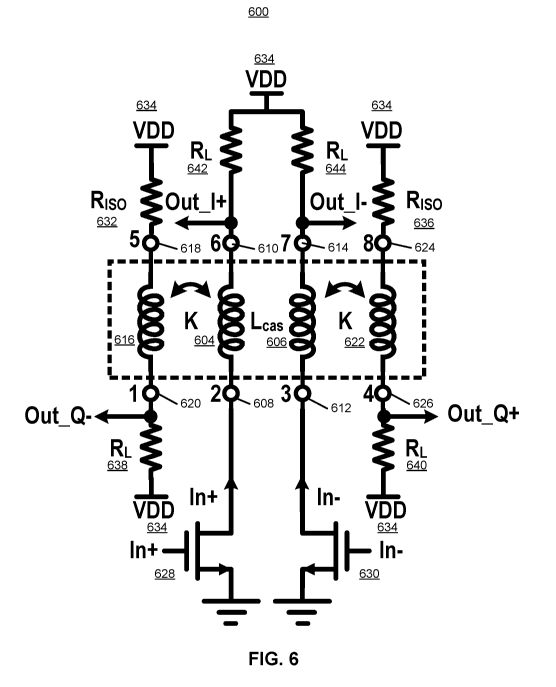
[0013] Figure 6 is a block diagram illustrating a transformer-based IQ
generator circuit with
an integrated amplifier circuit according to one embodiment.
[0014] Figure 7 is a block diagram illustrating a cascode transformer-based
IQ generator
circuit with an integrated amplifier circuit according to one embodiment.
[0015] Figures 8A-8B are block diagrams illustrating an example of a
conventional amplifier
and a differential transformer-based IQ generator circuit according to one
embodiment.
[0016] Figure 9 is a block diagram illustrating a transformer-based IQ
combiner circuit with
an integrated amplifier circuit according to one embodiment.
[0017] Figure 10 is a block diagram illustrating a cascode transformer-
based IQ combiner
circuit with an integrated amplifier circuit according to one embodiment.
3
CA 03202096 2023-05-15
WO 2022/106925 PCT/IB2021/059419
DETAILED DESCRIPTION
[0018] Various embodiments and aspects of the inventions will be described
with reference to
details discussed below, and the accompanying drawings will illustrate the
various embodiments.
The following description and drawings are illustrative of the invention and
are not to be construed
as limiting the invention. Numerous specific details are described to provide
a thorough
understanding of various embodiments of the present invention. However, in
certain instances,
well-known or conventional details are not described in order to provide a
concise discussion of
embodiments of the present inventions.
[0019] Reference in the specification to "one embodiment" or "an
embodiment" means that a
particular feature, structure, or characteristic described in conjunction with
the embodiment can
be included in at least one embodiment of the invention. The appearances of
the phrase "in one
embodiment" in various places in the specification do not necessarily all
refer to the same
embodiment.
[0020] Note that in the corresponding drawings of the embodiments, signals
are represented
with lines. Some lines may be thicker, to indicate more constituent signal
paths, and/or have arrows
at one or more ends, to indicate primary information flow direction. Such
indications are not
intended to be limiting. Rather, the lines are used in connection with one or
more exemplary
embodiments to facilitate easier understanding of a circuit or a logical unit.
Any represented signal,
as dictated by design needs or preferences, may actually comprise one or more
signals that may
travel in either direction and may be implemented with any suitable type of
signal scheme.
[0021] Throughout the specification, and in the claims, the term
"connected" means a direct
electrical connection between the things that are connected, without any
intermediary devices. The
term "coupled" means either a direct electrical connection between the things
that are connected,
or an indirect connection through one or more passive or active intermediary
devices. The term
"circuit" means one or more passive and/or active components that are arranged
to cooperate with
one another to provide a desired function. The term "signal" means at least
one current signal,
4
CA 03202096 2023-05-15
WO 2022/106925 PCT/IB2021/059419
voltage signal or data/clock signal. The meaning of "a", "an", and "the"
include plural references.
The meaning of "in" includes "in" and "on".
[0022] As used herein, unless otherwise specified the use of the ordinal
adjectives "first,"
"second," and "third," etc., to describe a common object, merely indicate that
different instances
of like objects are being referred to, and are not intended to imply that the
objects so described
must be in a given sequence, either temporally, spatially, in ranking or in
any other manner. The
term "substantially" herein refers to being within 10% of the target.
[0023] For purposes of the embodiments described herein, unless otherwise
specified, the
transistors are metal oxide semiconductor (MOS) transistors, which include
drain, source, gate,
and bulk terminals. Source and drain terminals may be identical terminals and
are interchangeably
used herein. Those skilled in the art will appreciate that other transistors,
for example, Bi-polar
junction transistors-BJT PNP/NPN, BiCMOS, CMOS, etc., may be used without
departing from
the scope of the disclosure.
[0024] According to one aspect, a transformer-based in-phase and quadrature
(IQ) includes a
differential balun having a first inductor and a second inductor. The first
inductor has a first input
terminal and a first output terminal. The second inductor has a second input
terminal and a second
output terminal. Additionally, the IQ generator circuit includes a third
inductor magnetically
coupled with the first inductor. The third inductor has a first isolation
terminal and a third output
terminal. The IQ generator circuit also includes a fourth inductor
magnetically coupled with the
second inductor. The fourth inductor has a second isolation terminal and a
fourth output terminal.
The IQ generator circuit additionally includes a first transistor coupled to
the first input terminal
of the first inductor. Further, the generator circuit includes a second
transistor coupled to the
second input terminal of the second inductor. The first transistor, the second
transistor, the first
inductor, and the second inductor form part of a differential amplifier.
[0025] In one embodiment, the IQ generator circuit further includes a first
resistor coupled to
between the first isolation terminal of the third inductor and a voltage
source. In addition, the IQ
CA 03202096 2023-05-15
WO 2022/106925 PCT/IB2021/059419
generator circuit includes a second resistor coupled to between the second
isolation terminal of the
fourth inductor and the voltage source.
[0026] In one embodiment, the IQ generator circuit also includes a third
resistor coupled
between the third output terminal and the voltage source. The IQ generator
circuit further includes
a fourth resistor coupled between the fourth output terminal and the voltage
source.
[0027] In one embodiment, the first resistor and the third resistor are
configured to have
resistance such that an amount of direct current (DC) flowing through the
third inductor is below
a first predetermined threshold.
[0028] In one embodiment, the second resistor and the fourth resistor are
configured to have
resistance such that that an amount of direct current (DC) flowing through the
fourth inductor is
below a second predetermined threshold.
[0029] In one embodiment, the IQ generator circuit further includes a fifth
resistor coupled
between the first output terminal and a voltage source. The IQ generator
circuit also includes a
sixth resistor coupled between the second output terminal and the voltage
source.
[0030] In one embodiment, the first output terminal represents a positive
in-phase (I+) output
terminal to output an I+ signal. In addition, the second output terminal
represents a negative in-
phase (I-) output terminal to output an I- signal.
[0031] In one embodiment, the third output terminal represents a negative
quadrature-phase
(Q-) output terminal to output a Q- signal. Additionally, the fourth output
terminal represents a
positive quadrature-phase (Q+) output terminal to output a Q+ signal.
[0032] In one embodiment, the inputs of the first and second transistors
are configured to
receive differential input signals.
[0033] In one embodiment, the IQ generator circuit also includes a third
transistor coupled
between the first transistor and the first input terminal. The IQ generator
circuit additionally
includes a fourth transistor coupled between the second transistor and the
second input terminal.
The first inductor, the second inductor, the first transistor, the second
transistor, the third transistor,
and the fourth transistor can form a part of a cascode amplifier.
6
CA 03202096 2023-05-15
WO 2022/106925 PCT/IB2021/059419
[0034] According to another aspect, a transformer-based IQ combiner circuit
with an
integrated amplifier can include a differential balun including a first
inductor and a second
inductor. The first inductor may have a first input terminal and a first
output terminal. The second
inductor may have a second input terminal and a second output terminal. The
combiner circuit
can also include a third inductor magnetically coupled with the first
inductor. The third inductor
may have a first isolation terminal and a third input terminal. Additionally,
the combiner circuit
can include a fourth inductor magnetically coupled with the second inductor.
The fourth inductor
may have a second isolation terminal and a fourth input terminal. The combiner
circuit may
additionally include a first transistor coupled to the first input terminal of
the first inductor.
Further, a second transistor coupled to the second input terminal of the
second inductor, wherein
the first transistor, the second transistor, the first inductor, and the
second inductor form a part of
an in-phase differential amplifier.
[0035] Figure 1 is a block diagram illustrating an example of a wireless
communication device
according one embodiment of the invention. Referring to Figure 1, wireless
communication device
100, also simply referred to as a wireless device, includes, among others, an
RF frontend module
101 and a baseband processor 102. Wireless device 100 can be any kind of
wireless communication
device such as, for example, mobile phones, laptops, tablets, network
appliance devices (e.g.,
Internet of thing or TOT appliance devices), etc.
[0036] In a radio receiver circuit, the RF frontend is a generic term for
all the circuitry between
the antenna up to and including the mixer stage. It consists of all the
components in the receiver
that process the signal at the original incoming radio frequency, before it is
converted to a
lower frequency, e.g., IF. In microwave and satellite receivers it is often
called the low-noise
block (LNB) or low-noise downconverter (LND) and is often located at the
antenna, so that the
signal from the antenna can be transferred to the rest of the receiver at the
more easily handled
intermediate frequency. A baseband processor is a device (a chip or part of a
chip) in a network
interface that manages all the radio functions (all functions that require an
antenna).
7
CA 03202096 2023-05-15
WO 2022/106925 PCT/IB2021/059419
[0037] In
one embodiment, RF frontend module 101 includes one or more RF transceivers,
where each of the RF transceivers transmits and receives RF signals within a
particular frequency
band (e.g., a particular range of frequencies such as non-overlapped frequency
ranges) via one of
a number of RF antennas. The RF frontend IC chip further includes an IQ
generator and/or a
frequency synthesizer coupled to the RF transceivers. The IQ generator or
generation circuit
generates and provides an LO signal to each of the RF transceivers to enable
the RF transceiver to
mix, modulate, and/or demodulate RF signals within a corresponding frequency
band. The RF
transceiver(s) and the IQ generation circuit may be integrated within a single
IC chip as a single
RF frontend IC chip or package.
[0038]
Figure 2 is a block diagram illustrating an example of an RF frontend
integrated circuit
according to one embodiment of the invention. Referring to Figure 2, RF
frontend 101 includes,
among others, an IQ generator and/or frequency synthesizer 200 coupled to a RF
transceiver 211.
Transceiver 211 is configured to transmit and receive RF signals within one or
more frequency
bands or a broad range of RF frequencies via RF antenna 221. In one
embodiment, transceiver 211
is configured to receive one or more LO signals from frequency synthesizer
200. The LO signals
are generated for the one or more corresponding frequency bands. The LO
signals are utilized to
mix, modulate and are demodulated by the transceiver for the purpose of
transmitting and receiving
RF signals within corresponding frequency bands. Although there is only one
transceiver and
antenna shown, multiple pairs of transceivers and antennas can be implemented,
one for each
frequency band.
[0039]
Described herein is a transformer-based design IQ generation combining into
and co-
designing with amplifier gain and bandwidth expansion. Two
different scenarios of
Transmitter(TX)/Receiver(RX) will be described in details (see Figures 3A-3D)
to demonstrate
various co-design methods in both transmitter and receiver architecture.
Moreover, inductive
design to enhance amplifier operation at mm-Wave frequency is further mutually
and inductively
coupled to create transformer-based current reuse topology to reduce size and
power consumption.
As a result, an ultra-compact wideband image-rejection system and circuit
design can be
8
CA 03202096 2023-05-15
WO 2022/106925 PCT/IB2021/059419
implemented to support the next-generation 5G communication devices (e.g.,
wideband remote
radio unit) with high capacity requirements.
[0040] Figures 3A-3D are block diagrams illustrating an example of two
types of image
rejection architecture for TX and RX design according to one embodiment.
Referring to Figure
3A, for example, in RX IR architecture 300 and TX IR architecture 340, the
differential IQ
generation may be associated with RX/TX front end as well as with IF
amplifiers to achieve
wideband image rejection. To achieve a better input receiver sensitivity, the
wideband low noise
amplifier (LNA) 302 may be used as a first-stage amplifier. In one embodiment,
an RX chain may
receive an RF signal, via the antenna (e.g., differential-ended antenna 304),
from a remote device
and the RF signal is amplified by the wideband LNA 302. As shown, the wideband
LNA 302
input may be directly connected to differential-ended antenna 304. The
wideband LNA 302 output
is fed into the differential IQ generation block 306.
[0041] Based on the differential input provided by LNA 302, IQ generation
block 306 (also
simply referred to as an IQ generator) generates an in-phase differential
output (I+/I-) and a
quadrature differential output (Q+/Q-). The I+/I- and Q+/Q- signals are then
down-converted
based on an LO signal 310 into intermediate frequency (IF) I+/I- and Q+/Q-
signals. The IF WI-
and Q+/Q- signals are then fed to an IQ combiner 380 (with optional amplified
by an IF amplifier
314), which combines the IF I+/I- and Q+/Q- signals into IF differential
output signals to be
processed by other downstream components such as a baseband processor or
digital signal
processor (DSP). In one embodiment, LNA 302 and IQ generator 306 may be co-
designed to form
a transformer-based IQ generator circuit integrated with an amplifier therein,
which is represented
by a dotted block RX1 1. The term of "co-design" refers to designing and
configuring the
parameters of the IQ generator 306 and LNA 302 altogether to achieve optimum
performance,
which will be described in details further below.
[0042] As illustrated in Figure 3B, which represents an RF transmitter, the
wideband power
amplifier (PA) 342 differential output is connected to the differential IQ
combiner block 344 and
then co-designed to differential-ended antenna 346 for maximizing the output
power and
9
CA 03202096 2023-05-15
WO 2022/106925 PCT/IB2021/059419
transmitter efficiency. For the TX/RX IR architecture 1 as depicted in Figures
3A-3B, differential
IQ generation may be processed in the RX/TX frontends and the IF amplifiers
with the node A
signal 308 including RF I+, RF I-, RF Q+, RF Q-, the node B signal 310
including LO +, LO-
-
, and the node C signal 312 including IF I+, IF I-, IF Q+, IF Q-. In one
embodiment, IQ
combiner 344 and PA 342 are co-designed represented by transformer-based block
TX1 1, and
similarly, the IQ generator 346 and IF amplifier 348 are co-designed
represented by transformer-
based block TX1 2.
[0043] In another embodiment as illustrated in Figures 3C-3D, the
differential IQ generation
may be associated with LO generation as well as with IF amplifiers to achieve
wideband image
rejection. As shown, for the TX/RX IR architecture 2 (e.g., 360 and 390),
differential IQ generation
can be processed in the LO generation with the node A 370 signal including RF
+, RF -, the node
B 372 signal including LO I+, LO I-, LO Q+, LO Q-, and the node C 374 signal
including IF I+,
IF I-, IF Q+, IF Q-. The differential IQ generation is preceded with LO
buffers 362 and the IF
amplifiers 364. For example, as illustrated in Figure 3C, the output of the LO
buffer 362 is fed
into the I/Q generation block 366. The output of IF amplifier 364 is fed into
the IQ combiner block
368.
[0044] In one embodiment, the IQ generation can be co-designed to provide
IQ signal
generation with amplifiers for differential signal inputs and differential IQ
signal outputs. In this
scenario, blocks RX1 1, RX2 1, TX1 2, TX2 1, and TX2 2 are referred (see
Figures 3A-3D).
In a second scenario, the IQ generation can be co-designed to provide
differential IQ signal inputs
and combined with differential IQ amplifiers for differential signal outputs
to finish image
rejection. In this second scenario, RX1 2, RX2 2, and TX1 1 can be referred.
[0045] Figure 4 illustrates an example of a differential transformer based
IQ generation 400.
As shown, the embodiment of the differential IQ generation is utilized via
transformer-based
structure to achieve a low-loss performance for generating differential in-
phase signal I (I+ and I-
at terminals 402 and 404) and quadrature signal Q (Q+ and Q- at terminals 406
and 408) based on
a differential input (In+, In-). Riso can be a loading impedance at isolation
terminals 410 and 412
CA 03202096 2023-05-15
WO 2022/106925 PCT/IB2021/059419
for the IQ generation. In this present disclosure, reused current
inductive/transformer-based design
concept is used to co-design and build ultra-compact active current IQ
generation amplifier.
[0046] Referring to Figure 5A, in conventional design of an amplifier, a
differential signal
(e.g., In+ and In-) is amplified by the differential amplifier 500 with
inductive load to generate the
differential output (Out+ 502 and Out- 504). Thereafter, the differential
output (Out+ 502 and
Out- 504) is fed into transformer-based differential IQ generation to generate
signals including
Out I+ 506, Out I- 508, Out Q+ 510, and Out Q- 512 (see Figure 5B). The
capacitor, C 514 (see
Figure 5A) at an amplifier output is used as DC-block to create an independent
biasing point as it
connects to the transformer-based IQ generation.
[0047] Figure 6 illustrates an example of a transformer-based in-phase and
quadrature (IQ)
generator circuit with an integrated amplifier according to an embodiment. In
some embodiments,
the IQ generator circuit 600 can include a differential balun having a first
inductor 604 and a
second inductor 606. As shown, the first inductor 604 can have a first input
terminal 608 and a
first output terminal 610. The second inductor 606 can have a second input
terminal 612 and a
second output terminal 614. Additionally, the IQ generator circuit 600 can
include a third inductor
616 magnetically coupled with the first inductor 604. The third inductor can
have a first isolation
terminal 618 and a third output terminal 620. The IQ generator circuit 600 can
also include a
fourth inductor 622 magnetically coupled with the second inductor 606. The
fourth inductor 622
can have a second isolation terminal 624 and a fourth output terminal 626. The
IQ generator circuit
600 can additionally include a first transistor 628 coupled to the first input
terminal 608 of the first
inductor 604. Further, the generator circuit 600 can include a second
transistor 630 coupled to the
second input terminal 612 of the second inductor 606.
[0048] In one embodiment, the first transistor 628, the second transistor
630, the first inductor
604, and the second inductor 606 form a part of a differential amplifier. In
this example, the
collector of the transistor 628 is coupled to the first input terminal 608,
while its emitter is coupled
to the ground. The base of the transistor 628 represents a differential input
terminal to receive a
differential input signal In+. Similarly, the collector of transistor 630 is
coupled to the second input
11
CA 03202096 2023-05-15
WO 2022/106925 PCT/IB2021/059419
terminal 612, while its emitter is coupled to the ground. The base of
transistor 630 represents a
differential input terminal to receive a differential input signal In-.
[0049] In one embodiment, the IQ generator circuit 600 can include a first
resistor 632 coupled
to between the first isolation terminal 618 of the third inductor 616 and a
voltage source.
Additionally, the IQ generator circuit 600 can include a second resistor 636
coupled to between
the second isolation terminal 624 of the fourth inductor 622 and the voltage
source 634.
[0050] In one embodiment, the IQ generator circuit 600 can include a third
resistor 638
coupled between the third output terminal 620 and the voltage source. The IQ
generator circuit
600 can also include a fourth resistor 640 coupled between the fourth output
terminal 626 and the
voltage source 634.
[0051] In one embodiment, the first resistor 632 and the third resistor 638
can be configured
to have resistance such that an amount of direct current (DC) flowing through
the third inductor
616 is below a first predetermined threshold.
[0052] In one embodiment, the second resistor 636 and the fourth resistor
640 can be
configured to have resistance such that an amount of direct current (DC)
flowing through the fourth
inductor 622 is below a second predetermined threshold.
[0053] In one embodiment, the IQ generator circuit 600 can include a fifth
resistor 642 coupled
between the first output terminal 610 and a voltage source 634. Additionally,
the IQ generator
circuit 600 can include a sixth resistor 644 coupled between the second output
terminal 614 and
the voltage source 634.
[0054] In one embodiment, the first output terminal 610 may represent a
positive in-phase (I+)
output terminal to output an I+ signal. The second output terminal 614 may
represent a negative
in-phase (I-) output terminal to output an I- signal.
[0055] In one embodiment, the third output terminal 620 may represent a
negative quadrature-
phase (Q-) output terminal to output a Q- signal. The fourth output terminal
626 may represent a
positive quadrature-phase (Q+) output terminal to output a Q+ signal.
12
CA 03202096 2023-05-15
WO 2022/106925 PCT/IB2021/059419
[0056] In one embodiment, inputs of the first transistor 628 and second
transistor 630 can be
configured to receive differential input signals.
[0057] The parameters of the amplifier and the IQ generator circuit are co-
designed. For
example, the gain of the amplifier may be determined based on the load
resistors 638 and 640, as
well as the coupled inductor turn ratio K. On the other hands, the pair of
resistors 632 and 638 are
designed with proper impedance, such that the DC current flowing through
inductor 616 can be
substantially eliminated or reduced. Similarly, the pair of resistors 636 and
640 are designed with
proper impedance, such that the DC current flowing through inductor 622 can be
substantially
eliminated or reduced.
[0058] Because of the inductive load Lcas an amplifier is first coupled as
a differential
transformer-based balun, these multi-inductors/transformers can reduce a bulky
conventional
design. Then, a transformer-based balun can be coupled with two inductors to
form a differential
IQ generation as illustrated in Figure 6. To provide load impedance for the
amplifier, the third
output terminal 620, fourth output terminal 626, the first output terminal
610, and the second output
terminal 614 can be loaded with RL to provide amplifier desired output
impedance. The amplifier
combines the inductive load to enhance current gain and further reuse the
current to form
transformer-based IQ generator circuit.
[0059] Moreover, to provide correct VDD biasing, the output load RL on the
third output
terminal 620, fourth output terminal 626, the first output terminal 610, and
the second output
terminal 614 can be connected to a voltage source 634. Since inductors or
transformers are DC-
short circuit, the biasing on the RISO in the first isolation terminal 618 and
the second isolation
terminal 624 are still VDD to make sure that there is no DC current flow
between the third output
terminal 620 and the first isolation terminal 618 to avoid extra DC power
consumption in the paths
on the third output terminal 620 and the first isolation terminal 618.
[0060] Similarly, for the reason discussed above, there is no DC current
flow between the
fourth output terminal 626 and the second isolation terminal 624 to avoid
extra DC power
consumption in the paths on the fourth output terminal 626 and the second
isolation terminal 624.
13
CA 03202096 2023-05-15
WO 2022/106925 PCT/IB2021/059419
In Figure 6, the Riso is now connected to VDD in comparison to GND in Figure
5B, which remain
the property of the differential IQ generation operation. This is because the
GND or VDD DC-
biasing for RF signal are served as RF-short. Therefore, the proposed
architecture 600 as described
above in Figure 6 can reuse the current and co-design with the differential IQ
generation with an
ultra-compact area without consuming any extra DC power penalty. In addition,
the proposed
architecture 600 does not require a capacitor at amplifier outputs as shown in
Figure 5A which is
lossy at RF frequency.
[0061] Figure 7 illustrates an example of a transformer-based in-phase and
quadrature (IQ)
generator circuit according to an embodiment. The architecture 600 described
in Figure 6 can be
extended to a cascode amplifier design for large output swing enhancement with
largely area
saving and bandwidth extension. The architecture 600 can be adaptable and
scalable in the case
for (a): IQ signal generation with amplifiers for differential signal inputs
and differential IQ signal
outputs, i.e., in building blocks cases: RX1 1, RX2 1, TX1 2, TX2 1, and TX2
2. In one
embodiment, the IQ generator circuit 700 can include a third transistor 746
coupled between the
first transistor 728 and the first input terminal 708. The IQ generator
circuit 700 can additionally
include a fourth transistor 748 coupled between the second transistor 730 and
the second input
terminal 712. The first inductor 704, the second inductor 706, the first
transistor 728, the second
transistor 730, the third transistor 746, and the fourth transistor 748 form a
part of a cascode
amplifier.
[0062] A cascade amplifier is a two-stage amplifier that consists of a
common-emitter stage
feeding into a common-base stage. Compared to a single amplifier stage, a
cascade amplifier may
have higher input-output isolation, higher input impedance, higher output
impedance, and higher
bandwidth. As shown in Figure 7, the collector of transistor 746 is coupled to
input terminal 708,
while its emitter is coupled to the collector of transistor 728. The base of
transistor 746 may be
coupled to a predetermined voltage (Vcas). Similarly, the collector of
transistor 748 is coupled to
input terminal 712, while its emitter is coupled to the collector of
transistor 730. The base of
14
CA 03202096 2023-05-15
WO 2022/106925 PCT/IB2021/059419
transistor 748 may be coupled to a predetermined voltage (Vcas). In one
embodiment, transistors
728, 730, 746, and 748 may be field-effect transistors (FETs).
[0063] Figures 8A-8B illustrate an example of a conventional amplifier and
a differential
transformer-based IQ combiner circuit according to one embodiment. Consider
blocks RX1 2,
RX2 2, and TX1 1 (see Figures 3A, 3B, and 3C), in conventional design,
differential IQ signal is
amplified by the differential IQ amplifier 800 with inductive load and then
the differential IQ
output signals (Out I+ 802, Out I- 804, Out Q+ 806, and Out Q- 808) are fed
into transformer-
based differential IQ combiner 820 (see Figure 8B) for IQ signal combination
and image rejection.
Thus, final differential output (Out Final+ 822 and Out Final- 824) can be
generated. As shown
in Figure 8A, the capacitor (e.g., 810) at the amplifier output is used as DC-
block to make
independent biasing point as it connects to the transformer-based IQ combiner
820.
[0064] Figure 9 illustrates a transformer-based in-phase and quadrature
(IQ) combiner circuit
900 with an integrated amplifier. In one embodiment, the combiner circuit 900
can include a
differential balun having a first inductor 904 and a second inductor 906. The
first inductor 904
can have a first input terminal 908 and a first output terminal 910. The
second inductor 906 can
have a second input terminal 912 and a second output terminal 914.
Additionally, the combiner
circuit 900 can include a third inductor 916 magnetically coupled with the
first inductor 904. The
third inductor 916 can have a first isolation terminal 918 and a third input
terminal 920. The
combiner circuit 900 can also include a fourth inductor 922 magnetically
coupled with the second
inductor 906. The fourth inductor 922 can have a second isolation terminal 924
and a fourth input
terminal 926.
[0065] In addition, the combiner circuit 900 can include a first transistor
928 coupled to the
first input terminal 910 of the first inductor 904. Further, the combiner
circuit 900 can also include
a second transistor 930 coupled to the second input terminal 914 of the second
inductor 906. The
first transistor 928, the second transistor 930, the first inductor 904, and
the second inductor 906
can form part of an in-phase differential amplifier.
CA 03202096 2023-05-15
WO 2022/106925 PCT/IB2021/059419
[0066] In one embodiment, the combiner circuit 900 can include a third
transistor 932 coupled
to the third input terminal 920 of the third inductor 916. The combiner
circuit 900 can also include
a fourth transistor 934 coupled to the fourth input terminal 926 of the fourth
inductor 922. The
third transistor 932, the fourth transistor 934, the third inductor 916, and
the fourth inductor 922
can form a part of a quadrature-phase differential amplifier.
[0067] In one embodiment, the third input terminal 920 may represent a
negative quadrature-
phase (Q-) input terminal and the fourth input terminal 926 may represent a
positive quadrature
(Q+) input terminal to receive a quadrature-phase differential signal from the
quadrature-phase
differential amplifier.
[0068] In one embodiment, the first input terminal 910 may represent a
positive in-phase (I+)
input terminal and the second input terminal 914 may represent a negative in-
phase (I-) input
terminal to receive an in-phase differential signal from the in-phase
differential amplifier. In one
embodiment, the first output terminal 908 and the second output terminal 912
may represent a
differential output of the IQ combiner circuit.
[0069] In one embodiment, the combiner circuit 900 can include a first
resistor 936 coupled
between the first isolation terminal 918 of the third inductor 916 and a
voltage source 938.
Additionally, the combiner circuit 900 can include a second resistor 940
coupled to the second
isolation terminal 924 of the fourth inductor 922 and the voltage source 938.
[0070] In one embodiment, the combiner circuit 900 can include a third
resistor 942 coupled
between the first output terminal 908 of the first inductor 904 and a voltage
source 938. In addition,
the combiner circuit 900 can include a fourth resistor 944 coupled to the
second output terminal
912 of the second inductor 906 and the voltage source 938. Again, the
transistors can be FETs.
[0071] Figure 10 illustrates a cascode transformer-based IQ combiner
circuit 1000 with an
integrated amplifier circuit according to some embodiments of the disclosure.
In one embodiment,
the combiner circuit 1000 can include a fifth transistor 1046 coupled between
the first transistor
1028 and the first input terminal 1010 of the first inductor 1004. The
combiner circuit 1000 can
also include a sixth transistor 1048 coupled between the second transistor
1030 and the second
16
CA 03202096 2023-05-15
WO 2022/106925 PCT/IB2021/059419
input terminal 1014 of the second inductor 1006. The first transistor 1028,
the second transistor
1030, the fifth transistor 1046, the sixth transistor 1048, the first inductor
1004, and the second
inductor 1006 can form a part of an in-phase differential cascode amplifier.
[0072] In one embodiment, the combiner circuit 1000 can include a seventh
transistor 1050
coupled between the third transistor 1032 and the third input terminal 1020 of
the third inductor
1016. The combiner circuit 1000 can additionally include an eighth transistor
1052 coupled
between the fourth transistor 1034 and the fourth input terminal 1026 of the
fourth inductor 1022.
The third transistor 1032, the fourth transistor 1034, the seventh transistor
1050, the eighth
transistor 1052, the third inductor 1016, and the fourth inductor 1022 can
form a part of a
quadrature-phase differential cascode amplifier.
[0073] In one embodiment, the first output terminal 1008 can be configured
to output a Final+
signal of the differential output of the IQ combiner circuit 1000.
Additionally, the second output
terminal 1012 can be configured to output a Final- signal of the differential
output of the IQ
combiner circuit 1000.
[0074] As further illustrated in Figure 9, all of inductive loads Lcas at
differential IQ amplifier
can be coupled as a differential IQ transformer. This configuration can reduce
multi-inductors or
transformers' bulky design as previously discussed. To provide load impedance
for the differential
IQ amplifier, the terminals 908, 912, 918, and 924 may be loaded with
resistors including RL to
provide the differential IQ amplifier desired output impedance at Out I+, Out
I-, Out Q+, and
Out Q- as shown in Figure 8A-8B. The differential IQ amplifier can combine the
inductive load
to enhance current gain and further reuse the current with a transformer-based
differential IQ
combiner to achieve image rejection at final outputs (e.g., 912 and 908).
Moreover, to provide
correct VDD biasing, the output load RL on the terminals 908, 912, 918, and
924 may be connected
to a voltage source 938.
[0075] As shown in Figure 9, note that RISO may be connected to a VDD 938.
In contrast,
RISO is connected to ground GND as illustrated in Figures 8A-8B. Again, this
is because the
GND or VDD DC-biasing for the RF signal is served as RF-short. Therefore, the
proposed
17
CA 03202096 2023-05-15
WO 2022/106925 PCT/IB2021/059419
architecture reuses the differential IQ current in the amplifiers and co-
designs with the differential
IQ combiner with an ultra-compact area to achieve low-cost image rejection.
This also removes
the need of a capacitor at differential IQ amplifier outputs as shown in
Figure 8A. This capacitor
can be lossy at RF frequency. Furthermore, the structure can be easily
extended to cascode
differential IQ amplifier for large output swing enhancement in Figure 10 with
a huge area saving
and bandwidth extension. The structure can be adaptable and scalable in the
case (b): serving as
differential IQ signal inputs and combined with differential IQ amplifiers for
differential signal
outputs to finish image rejection, i.e., in building blocks cases: RX1 2, RX2
2, and TX1 1.
[0076] In the foregoing specification, embodiments of the invention have
been described with
reference to specific exemplary embodiments thereof. It will be evident that
various modifications
may be made thereto without departing from the broader spirit and scope of the
invention as set
forth in the following claims. The specification and drawings are,
accordingly, to be regarded in
an illustrative sense rather than a restrictive sense.
18