Note: Descriptions are shown in the official language in which they were submitted.
WO 2022/194618 1
PCT/EP2022/055892
A solar cell comprising a plurality of porous layers and charge conducting
medium
penetrating the porous layers
Technical field
The present invention relates to solar cells for converting light energy into
electrical energy
comprising a plurality of porous layers and a charge conducting medium
penetrating the
porous layers.
Background
Solar cells for converting light into electrical energy comprising a plurality
of porous layers are
well known in the art.
Dye-sensitized solar cells (DSSC) comprising a porous light absorbing layer,
porous conductive
layers and a porous isolation layer are known to have a high potential for
industrial scale
manufacturing using established manufacturing methods such as screen printing,
inkjet
printing, or slot die coating.
Industrial scale manufacturing of dye sensitized solar cells involves
processing of large areas
of the thin layers of the solar cell components. These components undergo
various process
steps, like printing, heat treatments, vacuum treatments, chemical treatments
during
manufacturing. This means that to handle the processing of the solar cell, the
architecture of
the solar cell is important in order to be able to handle the components
mechanically and
perform the various treatments without damaging underlying components. The
architecture
of the solar cell is also important for the overall performance of the solar
cell.
A known procedure for manufacturing of dye sensitized solar cells is through a
roll-to-roll
2.5 process. In EnergyTrend 20180614 "Keys to Flexible Solar cell's Mass
Production: Cell
Encapsulation and Durability" the researchers describe that flexible DSSC
produced by a roll-
to-roll manufacturing process can be commercialized due to the efficiency of
the production
method.
In a roll-to-roll process, the solar cell comprises a solid substrate, like a
flexible conductive foil,
which can be placed on a conveyor belt and act as a mechanically stable
substrate for
positioning of other components of the solar cell. US8658455 describes a roll-
to-roll process
having a flexible substrate onto which a layer of TiO2 is formed and the TiO2
layer is sintered,
provided with dye and loaded with electrolyte after which a second flexible
substrate is added
on top for sealing the sandwich type DSSC. The sealing step also involving the
roll-to-roll
process is said to improve the risk of leakage or evaporation of liquid
electrolyte.
CA 03203444 2023- 6- 26
2
Flexible conductive foils are known, such as titanium, stainless steel or
other metal foils or
coated foils of conductive polymers or thin films of conductive glass.
A problem with the roll-to-roll manufacturing of dye sensitized solar cells
concerns that some
of the processes like heat treatments or vacuum treatments have to take place
as the
conveyor band rolls through the ovens or the chemical treatment boxes. This
requires space
and time for these processes.
Another way of manufacturing dye sensitized solar cell is described in
EP2834823B1 in which
a monolithic dye sensitized solar cell is shown in which all layers of
components are porous. A
porous insulating substrate made of woven and non-woven glass fibres acts as a
support
structure during the manufacturing and porous conductive metal layers are
printed onto both
sides of the porous insulating substrate. On one side the porous conductive
layer the TiO2
layer is printed and on the other side the porous conductive layer is provided
with a catalyst.
The TiO2 layer is immersed with a dye and an electrolyte is added as the cells
are cut into
suitable pieces for lamination of the protective foil. During the process
steps involving heat
treatments, vacuum treatment or various chemical treatments, the workpiece in
operation is
entirely porous and several workpieces can be stapled on top of each other
without hindering
for example released gases to be vented out. The porous insulating substrate
used as support
substrate in the manufacturing will be the insulating layer between the
working electrode and
the counter electrode in the final solar cell. The thickness of the porous
insulating substrate
will therefore be a trade-off between making the insulating layer thin enough
to reduce
resistive losses in the solar cell and making the porous substrate thick
enough to achieve
sufficient mechanical properties for serving as a support structure. During
the manufacturing,
the support structure must be turned in order to print on both sides of the
support.
EP1708301 discloses a dye sensitized solar cell with an architecture including
a stack of porous
layers arranged on top of each other, electrolyte integrally positioned in the
pores of the
porous layers and a support structure for supporting the stack of porous
layers made of
.. ceramic, metal, resin or glass.
Another problem with the dye-sensitized solar cells concerns evaporation or
depletion of
electrolytic solution or possible electrolytic leakage, especially during long-
term usage of the
solar cell.
Summary
It is an aim of the present invention to at least partly overcome the above
problem, and to
provide an improved solar cell.
This aim is achieved by a solar cell comprising a stack of porous layers, a
support substrate for
supporting the stack, and a charge conducting medium penetrating through the
stack,
Date Recue/Date Received 2023-09-08
2a
wherein the stack comprises: a porous light-absorbing layer, a porous first
conductive layer
including conductive material for extracting photo-generated electrons from
the light-
absorbing layer, a porous counter electrode including conductive material, and
a separating
layer made of porous electrically insulating material and arranged between the
first
conductive layer and the counter electrode, and where the first conductive
layer is arranged
closer to the light-absorbing layer than the counter electrode, wherein the
stack of porous
layers is arranged on top of the support substrate, the support substrate is
porous, and the
charge conducting medium is penetrating through the support substrate.
Date Recue/Date Received 2023-09-08
WO 2022/194618 3
PCT/EP2022/055892
The solar cell comprises a stack of porous layers arranged on top of each
other, a charge
conducting medium penetrating through the porous layers, and a support
substrate for
supporting the porous layers. The plurality of porous layers comprises a light-
absorbing layer,
a first conductive layer including conductive material for extracting photo-
generated electrons
from the light-absorbing layer, a counter electrode including conductive
material, and a
separating layer made of porous electrically insulating material and arranged
between the
first conductive layer and the counter electrode. The stack of porous layers
is arranged on top
of the support substrate, the support substrate is porous, and the charge
conducting medium
is penetrating through the porous support substrate.
The stack of porous layers are active layers, which means that they are
involved in the power
production. It is necessary that the charge conducting medium can penetrate
through the
stack of active porous layers to enable transport of charges between the light-
absorbing layer
and the counter electrode. The support substrate is not an active layer in the
solar cell, i.e. it
is not involved in the power production. The main function of the support
substrate is to serve
as a support for the stack of active layers.
The support substrate is porous and the charge conducting medium penetrates
the pores of
the substrate as well as the pores of the porous layers of the solar cell. Due
to the porosity of
the support substrate, the pores of the support substrate function as a
reservoir of charge
conducting medium. Thus, the total volume of charge conducting medium in the
solar cell is
increased. Consequentially, if the charge conducting medium in the solar cell
is decreasing due
to leakage or evaporation, the time until the total content of charge
conducing medium in the
solar cell has reach a minimum level and the solar cell stops working is
prolonged. The thicker
substrate and the higher porosity, the larger is the reservoir of charge
conducting medium.
Since the support substrate is not involved in the power generation, the
thickness of the
support substrate is not critical and does not affect the power generation.
Another advantage with the porous substrate is that it makes it easier to
achieve an even
filling of the charge conducting medium in the solar cell during manufacturing
of the solar cell.
This is a problem when thin and wide solar cells are manufactured. For
instance, the area of
the solar cell can be 1 m2 and the thickness of the solar cell can be 0.2 mm.
The charge
conducting medium has to be infiltrated into the porous layers of the large
solar cell, and
preferably all of the pores in the porous layers of the solar cell are filled
with the charge
conducting medium. Due to the porous substrate in the bottom of the solar
cell, the charge
conducting medium can be introduced from a bottom side of the solar cell and
by capillary
forces fill most of the pores in the porous layers in the stack with the
charge conducting
medium.
CA 03203444 2023- 6- 26
WO 2022/194618 4
PCT/EP2022/055892
Another advantage with the porous substrate is that vacuum filling of the cell
with conducting
medium, as in the prior art, is not needed. Vacuum filling is time consuming
and requires extra
equipment.
Another advantage with the porous substrate is that it retains the conducting
medium by
capillary forces and thereby prevents the conducting medium from pouring out.
Therefore, in
the case of breakage of the solar cell the conducting medium will be retained
in the porous
substrate and will not pour out.
Another advantage with having the porous layers stacked on a porous support
substrate
instead of a solid support substrate as in the prior art, is that it
facilitates manufacturing of
solar cells of large sizes since it allows gas to be emitted through the
substrate during vacuum
sintering of the solar cell and also during air sintering of the solar cell
where combustion gases
must be removed in later stages when layers comprising titanium dioxide, TiO2,
are air
sintered and combustion gases from organic substances have to be removed by
combustion.
Thus, production of the solar cell is speeded up.
The solar cell is preferably a monolithic cell. A monolithic solar cell is
characterized in that all
the porous layers are directly or indirectly deposited on one and the same
support substrate.
By having a porous support substrate at the bottom of the porous active
layers, the
manufacturing of the monolithic solar cell structure can profit from the
beneficial procedure
of stapling workpieces during the manufacturing process. Another advantage is
that a support
substrate at the bottom of the active layers and onto which the active layers
are formed is
that there is no need to turn the workpiece in operation during the
manufacturing process.
Another advantage of the present invention is that the separating layer made
of porous
electrically insulating material is not defined by the support substrate. The
porous separating
layer between the porous electrically conductive layers can be formed by a
cost-effective
printing process and be made by a variety of materials. The thickness of the
separating layer
can be designed to optimize the efficiency of the solar cell.
According to an aspect, the solar cell comprises an encapsulation
encapsulating the porous
layers, the support substrate, and the conducting medium, and the porous
layers are arranged
on one side of the support substrate, and an opposite side of the support
substrate is facing
the encapsulation.
Each of the porous layers and the support substrate has pores. The charge
conducting medium
is penetrating through the pores of the porous layers and the support
substrate. The charge
conducting medium is integrally positioned in the pores of the porous layers
and the pores of
the support substrate.
CA 03203444 2023- 6- 26
WO 2022/194618 5
PCT/EP2022/055892
According to an aspect, the average size of the pores of the plurality of
porous layers is smaller
than the average size of the pores of the support substrate so that the
capillary forces in the
pores of the porous layers are stronger than the capillary forces in the
support substrate. Due
to the fact that the pore sizes in the porous layers on top of the support
substrate are smaller
than the pore size in the support substrate, the capillary force of the porous
layers will
preferentially pump the charge conducting medium upwards where the capillary
forces are
stronger than the capillary forces in the support substrate. This action is
analogous to a
capillary pump action. This means in the presence of a leakage of charge
conducting medium
in the upper active layers, the charge conducting medium will preferentially
be pumped from
the reservoir upwards to the active layers, and the support substrate will act
as a reservoir
supplying charge conducting medium to the active layers.
The sizes of the pores in the substrate and the porous layers can, for
example, be measured
using a scanning electron microscope (SEM).
According to an aspect, at least 80% of the pores in the support substrate are
larger than 3
p.m, and at least 80% of the pores in the porous layers are smaller than 3
urn. Preferably, at
least 90% of the pores in the support substrate are larger than 3 m, and at
least 90% of the
pores in the porous layers are smaller than 3 urn. Preferably, at least 80% of
the pores in the
support substrate are between 3 pm and 10 urn, and most preferably at least
90% of the pores
in the support substrate are between 3 p.m and 10 m. Thus, the pores in the
porous layers
are typically in the sub meter range, i.e. below 3 p.m, and the pores in the
support substrate
are typically in the micrometre range, i.e. 3-10 p.m. The difference in pore
size between the
support substrate and the porous layers achieves that the capillary forces in
the porous layers
are stronger than the capillary forces in the support substrate, and
consequentially the charge
conducting medium will be pumped upwards to the active layers if the content
of charge
conducting medium in the active layers of the solar cell is reduced.
According to an aspect, the thickness of the support substrate is at least 20
p.m, preferably at
least 30 m, and most preferably at least 50 m. The thicker substrate, the
larger is the
reservoir of charge conducting medium.
According to an aspect, the thickness of the support substrate is between 20
p.m and 200
According to an aspect, the porosity of the support substrate is at least 50%,
and preferably
at least 70%, and most preferably at least 80 %. The higher porosity, the
larger is the reservoir
of charge conducting medium.
According to an aspect, the porosity of the support substrate is between 50%
and 90%, and
preferably between 70% and 90%.
According to an aspect, the support substrate comprises woven and/or non-woven
microfibers. A microfiber is a fibre having a diameter less than 10 m and
larger than 1 nm.
CA 03203444 2023- 6- 26
WO 2022/194618 6
PCT/EP2022/055892
According to an aspect, the support substrate comprises inorganic fibres.
According to an aspect, the support substrate comprises at least one of the
following: glass
fibres, ceramic fibres, and carbon fibres.
According to an aspect the microfibres have a diameter between 0.2 pm and 10
p.m,
preferably between 0.2 rim and 5 rim, more preferably between 0.2 pm and 3
rim, and most
preferably between 0.2 and 1 pm.
According to an aspect, the support substrate comprises a layer of woven
microfibers. Woven
microfibers are flexible, and accordingly the solar cell becomes flexible.
According to an aspect, the support substrate comprises a layer of non-woven
microfibers
arranged on the layer of woven microfibers. Woven microfibers and non-woven
microfibers
are flexible, and accordingly the solar cell becomes flexible. The non-woven
microfibers act as
a spring cushion effectively absorbing and dampening incoming mechanical
energy and also
distributes incoming mechanical energy over a larger area thereby reducing the
local effect.
An advantage with having the porous layers stacked on a substrate comprising a
layer of
woven microfibers and non-woven is that the support substrate becomes chock
absorbing and
therefore more mechanically robust in cases where the solar cell is subjected
to, e.g.,
mechanical bending or twisting or stretching or an impact hammer. This is an
advantage when
the solar cell is integrated into consumer products, such as headphones,
remote controls, and
cell phones.
According to an aspect the layer of non-woven microfibres is arranged closer
to the counter
electrode than the layer of woven microfibers. Preferably the layer of non-
woven microfibers
is contiguously arranged to the counter electrode.
According to another aspect the layer of woven microfibers is arranged closer
to the counter
electrode than the layer of non-woven microfibers. Preferably the layer of
woven microfibers
is contiguously arranged to the counter electrode.
According to an aspect the layer of woven microfibers comprises yarns with
holes formed
between them, and at least a part of the non-woven microfibers is accumulated
in the holes
between the yarns.
According to an aspect, the thickness of the separating layer is between 3 p.m
and 50 p.m, and
preferably between 4 p.m and 20 pm. It is a desire to make the separating
layer as thin as
possible to reduce resistive losses in the solar cell and accordingly improve
the efficiency of
the solar cell. However, if the separating layer becomes too thin, there is a
risk for short circuit
between the conductive layer and the counter electrode.
According to an aspect, the separating layer comprises porous electrically
insulating material.
Preferably the electrically insulating material is made of electrically
insulating particles. Such
a separating layer can be manufactured be applying several layers of
insulating particles on
CA 03203444 2023- 6- 26
WO 2022/194618 7
PCT/EP2022/055892
top of each other to achieve a desired thickness of the separating layer.
Thus, it is possible to
control the thickness of the separating layer and the thickness of the
separating layer can be
chosen depending on the need.
According to an aspect said electrically insulating particles consists of an
insulating material.
According to an aspect said electrically insulating particles comprises a core
of semi-
conducting material and an outer layer of an electrically insulating material
covering the core.
According to an aspect, the insulating material of the outer layer of the
insulating particles
comprises one or more of the materials in the group consisting of alumina
(A1203), zirconium
oxide (ZrO2), silicon oxide (SiO2), and aluminosilicate. The aluminosilicate
is, for example,
Al2Si05.
According to an aspect, the insulating material of the outer layer of the
insulating particles is
one or more of the materials in the group consisting of alumina (A1203),
zirconium oxide (ZrO2),
silicon oxide (SiO2), and aluminosilicate. The aluminosilicate is, for
example, Al2Si05.
According to an aspect the semiconducting material in the core of the
insulating particle
comprises titanium dioxide (TiO2).
According to an aspect the semiconducting material in the core of the
insulating particle is
titanium dioxide (TiO2).
According to an aspect the electrically insulating material of the insulating
particles comprises
one or more of the materials in the group consisting of alumina (A1203),
zirconium oxide (ZrO2),
silicon oxide (SiO2), and aluminosilicate. The aluminosilicate is, for
example, Al2Si05. According
to a further aspect the insulating material may be glass.
According to an aspect the electrically insulating material of the insulating
particles is one or
more of the materials in the group consisting of alumina (A1203), zirconium
oxide (ZrO2), silicon
oxide (SiO2), and aluminosilicate. The aluminosilicate is, for example,
Al2.5105. According to a
further aspect the insulating material may be glass.
According to an aspect, the charge conducting medium is a liquid electrolyte.
Certain conducting media, like copper complex electrolytes and cobalt complex
electrolytes,
can have very low electrical conductivity resulting in very large electrical
resistive losses. The
low electrical conductivity originates from the fact that the electrolytes
have large ions with
low diffusion rate. When a liquid electrolyte transport charges, the charges
move with
Brownian motion, i.e. they move randomly due to collisions with fast-moving
atoms or
molecules in the liquid. Copper and cobalt have relatively large ions that are
slow moving and
thus have low conductivity. The efficiency of using such electrolytes is
greatly improved by
having a short distance between the counter electrode and the light absorbing
layer. The
present invention makes it possible to choose the thickness of the separating
layer and
CA 03203444 2023- 6- 26
WO 2022/194618 8
PCT/EP2022/055892
accordingly select a suitable distance between the counter electrode and the
light absorbing
layer depending on the electrolyte.
According to an aspect, the conducting medium comprises copper complexes. An
advantage
with using copper complexes for charge transportation is that the conducting
medium will be
non-toxic. The use of copper as conducting medium has been shown to give a
very high
resulting photo voltage. The solar cell according to the invention allows the
use of copper
complexes due to the fact that the distance between the counter electrode and
the light
absorbing layer can be made short.
According to a further aspect the charge conducting medium comprises iodide
Oland triiodide
031.
Another object of the present invention is to provide a method for producing
the solar cell:
The method comprises:
- providing a porous support substrate,
- depositing a porous counter electrode on the porous support substrate,
- depositing a porous separating layer on the counter electrode,
- depositing a porous conductive layer on the separating layer,
- depositing a porous light-absorbing layer on the conductive layer,
- introducing a charge conducting medium into the stack and the support
substrate until the
charge conducting medium is penetrating the support substrate and the stack,
- sealing the solar cell.
According to an aspect depositing the porous counter electrode comprises
depositing a
porous second conductive layer and a porous catalytic layer on top of the
second conductive
layer.
According to an aspect the charge conducting medium is introduced on the side
of the
support substrate that is facing way from the stack such that the support
substrate and the
stack is impregnated with the charge conducting medium.
The depositing of the porous counter electrode, the porous separating layer,
the porous first
conductive layer and the porous light absorbing layer are, for example, done
by a spraying or
printing technique, such as ink jet printing or screen printing.
Brief description of the drawings
The invention will now be explained more closely by the description of
different embodiments
of the invention and with reference to the appended figures.
Fig. 1 shows a cross-section through an example of a solar cell according to
the invention.
CA 03203444 2023- 6- 26
WO 2022/194618 9
PCT/EP2022/05.5892
Fig. 2 shows a cross-section through another example of a solar cell according
to the invention.
Fig. 3 shows an SEM image of a cross section through an example of an
embodiment of the
invention.
Fig. 4 shows an SEM image of a cross section through another example of an
embodiment of
the invention.
Fig. 5 shows a block diagram of an example of a method of manufacturing the
solar cell
according to the invention.
Detailed description
Aspects of the present disclosure will be described more fully hereinafter
with reference to
the accompanying drawings. The solar cell device can, however, be realized in
many different
forms and should not be construed as being limited to the aspects set forth
herein. Like
numbers in the drawings refer to like elements throughout.
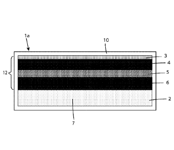
Figure 1 shows a cross-section through an example of a solar cell la according
to the invention.
The solar cell la comprises a support substrate 2 and a stack 12 of porous
layers 3 - 6 arranged
1.5 on top of the support substrate 2. The stack 12 of porous layers
comprise a light-absorbing
layer 3, which serves as a working electrode, a conductive layer 4 made of
porous conducting
material, which serve as a current collector, a separating layer 5 comprising
porous electrically
insulating material, and a counter electrode 6 comprising porous conducting
material. The
counter electrode 6 is formed on one side of the porous substrate 2. In this
example, the
counter electrode is a porous conductive layer. The separating layer 5 is
arranged between
the counter electrode 6 and the conductive layer 4. The separating layer 5
serves the function
of separating the conductive layer 4 and the counter electrode 6 physically
and electrically to
avoid direct electronic short circuit between them. In this example, the
separating layer .5 is
formed on the counter electrode 6 and the conductive layer 4 is formed on the
separating
layer 5. The light-absorbing layer 3 is arranged on top of the conductive
layer 4. The first
conductive layer 4 includes conductive material for extracting photo-generated
electrons
from the light-absorbing layer 3. The light absorbing layer 3 can be made in
different ways.
For example, the light absorbing layer may comprise dye molecules adsorbed on
surfaces of
semiconducting particles, or clusters of dye, or grains made of a
semiconducting material, such
as silicon.
The porous layers 3-6 are active layers, which means that they are involved in
the power
production. The support substrate 2 is not an active layer in the solar cell,
i.e. it is not involved
in the power production. The support substrate 2 supports the stack 12 of
porous layers 3-6.
Further, the support substrate 2 allows the counter electrode 6 to be printed
on it during
manufacturing of the solar cell. The porous layers 3-6 are arranged on one
side of the support
substrate 2.
CA 03203444 2023- 6- 26
WO 2022/194618 10
PCT/EP2022/055892
Each of the porous layers formed on the support substrate has a large number
of pores. The
solar cell further comprises a charge conducting medium 7 penetrating the
pores of porous
layers 3-6 to enable transport of charges between the light-absorbing layer 3
and the counter
electrode 6. The support substrate 2 is also porous and include pores. The
charge conducting
medium 7 penetrates the pores of the support substrate 2 as well as the pores
of the porous
layers 3-6 of the solar cell. Due to the porosity of the support substrate 2,
the pores of the
support substrate function as a reservoir of charge conducting medium.
In one aspect, the average size of the pores of the porous layers 3 - 6 in the
stack 12 is smaller
than the average size of the pores of the support substrate 2 so that the
capillary forces in the
pores of the porous layers 3-6 are stronger than the capillary forces in the
support substrate
2. The difference in pore size between the support substrate 2 and the porous
layers 3-6
makes the capillary forces in the porous layers stronger than the capillary
forces in the support
substrate 2, and consequentially the charge conducting medium 7 will be pumped
upwards to
the active layers 3-6, if the content of charge conducting medium in the
active layers of the
solar cell is reduced.
Preferably, at least 80% of the pores in the support substrate 2 are larger
than 3 pm, and at
least 80% of the pores in the porous layers are smaller than 3 p.m. More
preferably, at least
90% of the pores in the support substrate 2 are larger than 3 urn, and at
least 90% of the pores
in the porous layers 3-6 are smaller than 3 urn. For example, at least 80% of
the pores in the
support substrate 2 are between 3 rn and 10 p.m.
The thicker support substrate 2, the larger is the reservoir of charge
conducting medium in
the solar cell. Typically, the thickness of the support substrate 2 is between
20 p.m and 200
pm. Preferably, the thickness of the support substrate is at least 30 p.m.
The higher porosity in the support substrate, the larger reservoir of charge
conducting
medium 7. Preferably, the porosity of the support substrate is at least 50%,
and most
preferably at least 70%. If the support substrate is too porous the mechanical
strength of the
substrate will be too low. Preferably, the porosity of the support substrate
is between 50%
and 90%.
The solar cell further comprises an encapsulation 10 encapsulating the porous
layers 3-6, the
support substrate 2, and the conducting medium 7. The stack 12 of porous
layers is arranged
on one side of the support substrate 2, and an opposite side of the support
substrate is facing
the encapsulation 10.
The stack 12 of porous layers may include other porous layers arranged between
the porous
layers 3-6. For example, there can be a porous catalytic layer disposed
between the support
substrate 2 and the counter electrode 6, or between the counter electrode 6
and the
CA 03203444 2023- 6- 26
WO 2022/194618 11
PCT/EP2022/055892
separating layer 5, as shown in figure lb. Further, there can be a porous
reflective layer
arranged between the conductive layer 4 and the light-absorbing layer 3. The
same conditions
as mentioned above regarding the pore size applies for all layers in the stack
12 of porous
layers independent om the number of layers.
Figure 2 shows a cross-section through another example of a solar cell lb
according to the
invention. The solar cell lb comprises a support substrate 2 and a stack 12 of
porous layers 3
- 6 arranged on top of the support substrate 2. The solar cell lb differs from
the solar cell la
in that the the counter electrode 6 of the solar cell lb comprises a second
porous conductive
layer 6a and a porous catalytic layer 6b formed on top of the porous
conductive layer 6a.
In this example, the support substrate 2 comprises a layer of woven
microfibers 2a and a layer
of non-woven microfibers 2b arranged on the layer of woven microfibers 2a. The
counter
electrode 6 is disposed on the layer of non-woven microfibers 2b. In this
example, the porous
conductive layer 6a of the counter electrode 6 is formed on the layer of non-
woven
microfibers 2b. Alternatively, the catalytic layer 6b is disposed on the layer
of non-woven
microfibers 2b. The layer 2a of woven microfibers comprises yarns with holes
formed between
them, and at least a part of the non-woven microfibers is accumulated in the
holes between
the yarns. Preferably, the microfibers in the layer 6b of non-woven
microfibers have a
diameter between 0.2 p.m and 5 p.m, to achieve pores having a size above 1
p.m. EP2834824B1
discloses methods for manufacturing a substrate 2 comprising woven as well as
non-woven
microfibers.
The solar cells la and lb are of monolithic type. This means that all the
porous layers are
directly or indirectly deposited on the same support substrate 2. The solar
cells la and lb can,
for example, be dye sensitized solar cells (DSC).
Fig. 3 shows an SEM image of a cross section through an example of an
embodiment of the
invention showing the support substrate 2 comprising the layer of woven
microfibers 2a on
top of the layer of non-woven microfibers 2b. On support substrate 2 the
second porous
conductive layer 6a is arranged, thereafter the catalytic layer 6b, and on top
of the catalytic
layer the separating layer 5. On top of the separating layer 5 the first
conductive layer 4 is
arranged and thereon the light absorbing layer 3.
Fig. 4 shows an SEM image of a cross section through another example of an
embodiment of
the invention showing a support substrate 2 comprising a layer of non-woven
microfibers 2b
on top of a layer of woven microfibers 2a. On support substrate 2 the second
porous
conductive layer 6a is arranged, thereafter the catalytic layer 6b, and on top
of the catalytic
layer the separating layer 5. On top of the separating layer 5 the first
conductive layer 4 is
arranged and thereon the light absorbing layer 3.
CA 03203444 2023- 6- 26
WO 2022/194618 12
PCT/EP2022/05.5892
Preferably, the pore size of the light-absorbing layer 3 is equal or smaller
than the pore size of
the first conductive layer 4, the pore size of the first conductive layer 4 is
equal or smaller than
the pore size of the separating layer 5, and the pore size of the separating
layer 5 is equal or
smaller than the pore size of the layers of the counter electrode 6, 6a, 6b.
The pore size of
counter electrode 6, 6a, 6b is preferably smaller than the pore size of the
support substrate 2,
2a,2b.
In one embodiment of the invention, the pore size in the stack 12 of porous
layers decrease
from the counter electrode 6 to the light absorbing layer 3. For example, the
pore size of the
light-absorbing layer 3 is smaller than the pore size of the first conductive
layer 4, the pore
size of the first conductive layer 4 is smaller than the pore size of the
separating layer 5, and
the pore size of the separating layer 5 is smaller than the pore size of the
counter electrode 6,
6a, 6b. The pore size of the counter electrode 6, 6a, 6b is smaller than the
pore size of the
support substrate 2, 2a,2b. This embodiment will strengthen the difference in
capillary forces
in the porous layers compared to the capillary forces in the support substrate
2.
The light absorbing layer 3 is facing the incident light. The light absorbing
layer 3 can be made
in different ways. For example, the light absorbing layer 3 may comprise a
porous TiO2 layer
deposited onto the first conducting layer 4. The TiO2 layer may comprise TiO2
particles having
dye molecules absorbed on their surfaces. In another example, the light
absorbing layer 3
comprise a plurality of grains of a doped semiconducting material, such as
silicon, deposited
on the conducting layer 4. The charge conducting medium is integrally
positioned in pores
formed between the grains. The thickness of the light absorbing layer 3 can
vary and depends
on the type of the light absorbing layer 3.
The top side of the solar cell 1a;1b should be facing the light to allow the
light to hit the
light-absorbing layer 3. According to some aspects, the light absorbing layer
is a porous TiO2
nanoparticle layer with adsorbed organic dye or organometallic dye molecules
or natural
dye molecules. However, the light-absorbing layer 3 may also comprise grains
of a doped
semiconducting material, for example, Si, CdTe, CIGS, CIS, GaAs, or
perovskite.
The conductive layer 4 serves as a back contact that extracts photo-generated
charges from
the light absorbing layer 3. The porosity of the conductive layer 4 can
preferably be between
30% and 85%. Depending on which material is used for the conductive layer 4
and which
manufacturing method is used, the thickness of the conductive layer 4 can vary
between 1km
and 50 p.m. For example, the conductive layer 4 is made of a material selected
from a group
consisting of titanium, titanium alloys, nickel alloys, graphite, and
amorphous carbon, or
mixtures thereof. Most preferably, the conductive layer is made of titanium or
a titanium alloy
or mixtures thereof. In such case, the thickness of the conductive layer 4 is
preferably between
4 p.m and 30 rn.
CA 03203444 2023- 6- 26
WO 2022/194618 13
PCT/EP2022/055892
The separating layer 5 serve as an electrical separating between the
conductive layer 4 and
the counter electrode 6 to avoid short circuit between them. The distance
between the
counter electrode 2 and the light absorbing layer 3 depends on the thickness
of the separating
layer 5 and should be as small as possible so that the transport of charges
between the counter
electrode 2 and the light absorbing layer 3 becomes as fast as possible and
consequentially to
reduce resistive losses in the solar cell. The thickness of the separating
layer is, for example,
between 3 p.m and 50 p.m, and preferably between 4 km and 20 p.m. The
separating layer
comprises porous electrically insulating material. For example, the separating
layer comprises
a porous layer of electrically insulating particles. For example, the
insulating particles have a
1.0 core of a semiconducting material and an outer layer of electrical
insulating material. For
example, a layer of insulating oxide is formed on the surfaces of the
semiconducting material.
Suitably, the semiconducting material is titanium dioxide (TiO2). The
insulating material is, for
example, alumina or silicon oxide. Alternatively, the entire particles may be
of insulating
material, for example, alumina (A1203), silicon oxide (SiO2), or zirconium
oxide (ZrO2).
The counter electrode 6 comprises a porous conducting layer 6a. The counter
electrode
normally also comprises a catalytic layer 6b. The counter electrode 6 can have
a separate
porous catalytic layer 6b or have catalytic particles integrated in the porous
conducting layer
6a. The porosity of the counter electrode 6 can preferably be between 30% and
85%.
Depending on which material is used for the counter electrode 6 and the
manufacturing
method, the thickness of the counter electrode 6 can vary between 1 p.m and 50
p.m. For
example, the counter electrode 6 is made of a material selected from a group
consisting of
titanium, titanium alloys, nickel alloys, graphite, and amorphous carbon, or
mixtures thereof.
Most preferably, the counter electrode 6 is made of titanium or a titanium
alloy or mixtures
thereof. In such case, the sickness of the conductive layer 4 preferably is
between 10 p.m and
tim. To achieve a catalytic effect, the counter electrode 6 may include
platinized particles
of conductive metal oxides, such as platinized ITO, ATO, PTO, and FTO, or
particles of
platinized carbon black or graphite.
30 The support substrate 2, can be a microfiber-based substrate, such as
glass microfiber
substrate or ceramic microfiber substrate. The support substrate 2 is suitable
made of
microfibers. A microfiber is a fibre having a diameter less than 10 [irn and
length larger than 1
nm. Suitably, the support substrate 2 comprises woven microfibers. The
microfibers can be
made of a refractory and inert material, such as glass, 5i02, A1203 and
aluminosilicate. Organic
microfibers are fibres made of organic materials such as polymers such as,
e.g.,
polycap rolactone, PET, PEO etc, or cellulose such as, e.g., nanocellulose
(MFC) or wood pulp.
The support substrate 2 may comprise woven microfibers and non-woven
microfibers
disposed on the woven microfibers. Suitably, the support substrate 2 comprises
fiberglass. For
example, the porous support substrate can be made of woven and non-woven glass
fibers.
The thickness of the support substrate 2 is suitably between 10 p.m and 1 mm.
Such a layer
provides the required mechanical strength.
CA 03203444 2023- 6- 26
WO 2022/194618 14
PCT/EP2022/055892
The charge conducting medium 7 is integrally positioned in the in pores of the
porous layers
3-6 and the pores of the support substrate 2 and transfers charges between the
counter
electrode 6 and the light absorbing layer 3. The conducting medium 7 can be
any suitable
conducting medium, such as a liquid, a gel, or a solid material such as a
semiconductor.
Examples of electrolytes are liquid electrolytes, such as those based on
iodide(1)/triiodide(13-)
-ions or cobalt complexes as redox couple, or gel electrolytes, ordinary
polymer electrolytes.
Preferably, the conducting medium is a liquid electrolyte, such as an ionic
liquid-based
electrolyte, a copper-complex based electrolyte, or a cobalt-complex based
electrolyte.
The solar cells must be properly sealed to avoid leakage of the charge
conducting medium.
For example, the solar cell is provided with the encapsulation 10 enclosing
the solar cell unit.
However, the encapsulation must be penetrated in some way to enable access to
the power
produced by the solar cell. Although, the penetrations are sealed, there is a
risk for a slow
leakage of the charge conducting medium from the solar cell. Leakage may also
occur from
the sealed edges of the encapsulation. The slow leakage of charge conducting
medium will
cause a slow deterioration of the efficiency of the solar cell. When the
content of charge
conducing medium in the solar cell has reached a minimum level, the light to
electricity
converting ability of the solar cell will decrease. This process can take
several months or even
years depending on the quality of the encapsulation and the sealing.
The encapsulation 10 acts as barriers in order to protect the solar cell
against the surrounding
atmosphere, and to prevent the evaporation or leakage of the charge conducting
medium
from inside the cell. The encapsulation 10 may include an upper sheet covering
a top side of
the solar cell and a lower sheet covering a bottom side of the solar cell. The
upper sheet on
the top side of the solar cell covers the light absorbing layer and needs to
be transparent,
allowing light to pass through. A bottom side of the support substrate 2 is
facing the lower
sheet of the encapsulation 10. The light-absorbing layer 3 is facing the upper
sheet of the
encapsulation 10. The upper and lower sheets are, for example, made of a
polymer material.
The edges of the upper and lower sheets are sealed.
According to one aspect the encapsulation 10 of the solar cell 1a4b comprises
a plurality of
penetration openings (not shown in figures) to enable access to the power
produced by the
solar cell. The penetration openings receive wires to electrically connect to
the first conductive
layer 4 and the counter electrode 6. The penetration openings may be arranged
in connection
to the first conductive layer 4 and the counter electrode 6. Preferably the
penetration
openings are arranged in the side of the encapsulation arranged below the
support substrate
7.
Fig. 5 shows a block diagram of an example of a method of manufacturing the
solar cell
according to the invention. The method in figure 5 comprises the following
steps:
CA 03203444 2023- 6- 26
WO 2022/194618 15
PCT/EP2022/055892
Si: providing a porous support substrate 2,
S2: depositing a porous counter electrode 6 on the porous support substrate 2,
S3: depositing a porous separating layer 5 on the counter electrode 6,
S4: depositing a first porous conductive layer 4 on the separating layer 5,
S5: depositing a porous light-absorbing layer 3 on the first conductive layer
4,
S6: introducing a charge conducting medium 7 into the stack 12 and the support
substrate 2
until the charge conducting medium 7 is penetrating the support substrate 2
and the stack
12,
S7: sealing the solar cell.
According to one aspect the charge conducting medium 7 is introduced on the
side of the
support substrate that is facing way from the stack 12 such that the support
substrate and
the stack is impregnated with the charge conducting medium.
The depositing in steps S2- S5 is, for example, done by a spraying or printing
technique, such
as ink jet printing or screen printing.
An example of how the step S3 can be carried out will now be explained in more
details. A
separator ink is prepared by mixing a powder of insulating particles with a
solvent, a dispersing
agent, and a binder. The solvent is, for example, water or an organic solvent.
The binder is, for
example, hydroxy propyl cellulose. The dispersing agent is, for example, Byk
180. The mixture
is stirred until aggregated particles in the powder are separated into single
particles, and the
particles in the ink is well dispersed. The separator ink is deposited on the
counter electrode
6 by a spraying or printing technique. The depositing of the separator ink can
be repeated two,
three, or more times until a sufficiently thick layer of insulating particles
has be deposited on
the counter electrode. Preferably, the layer of separator ink is dried before
the next layer of
separator ink is deposited on the previous layer of separator ink. It is
advantageous to repeat
the depositing of the separator ink two or more times since the following
layers of ink will
repair possible defects in the previous layers of insulating particles. Is it
important that there
are no defects, such as, cracks or holes, in the separating layer 5 since this
will lead to short
circuit between the counter electrode 6 and the porous first conductive layer
4.
The solar cell la in figure 1 is infiltrated with a charge conducting medium 7
in the pores of
the light absorbing layer 3, in the pores of the first conductive layer 4, in
the pores of the
separating layer 5, in the pores of the counter electrode 6 and in the pores
of the support
substrate 2. The charge conducting medium forms a continuous layer inside the
pores of the
conducting layers, and between the conducting layers inside the pores of the
separating
layer thereby enabling transport of electrical charge between the counter
electrode 6 and
the working electrode including the first conductive layer 4 and the light
absorbing layer 3.
The first porous conductive layer 4 extracts the electrons from the light
absorbing layer 3
CA 03203444 2023- 6- 26
WO 2022/194618 16
PCT/EP2022/055892
and transports the electrons to an external electrical circuit connected to
the counter
electrode 6 (not shown in fig. 1). The counter electrode 6 is used to transfer
the electrons to
the charge conducting medium 7. The conducting medium 7 transfers electrons
back to the
light absorbing layer 3 thereby completing the electrical circuit.
Depending on the nature of the charge conducting medium 7, either ions or
electrons and
holes can be transported between the counter electrode and the working
electrode.
Electrolytes in dye-sensitized solar cells are normally classified as liquid
electrolytes, quasi-
solid-state electrolytes, or solid-state electrolytes. The electrolytes can be
in the form of a
liquid, gel or in solid state. There are a large number of electrolytes of
either type known in
literature, see for example Chemicals Reviews, Jan 28, 2015, "Electrolytes in
Dye-Sensitized
Solar Cells". The electrolytes are an expensive component of the Dye-
Sensitized Solar Cells.
The counter electrode is normally equipped with a catalytic substance 6b that
serves the
purpose of facilitating the transfer of electrons to the electrolyte.
The charge conducting medium exhibits a certain electrical resistance to
transport charges.
The electrical resistance increases with the charge transport distance.
Therefore, when
electrical charge is transported between the counter electrode and the light
absorbing layer,
there will always be a certain electrical resistive loss in the conducting
medium. By making the
porous substrate thinner, the resistive losses can be reduced. However, when
the porous
substrate becomes thinner it also becomes more mechanically fragile.
The conducting medium is, for example, a conventional 1113- electrolyte or a
similar
electrolyte, or a Cu-/Co- complex electrolyte. Solid state transition metal-
based complexes or
organic polymer hole conductors are known conducting mediums.
According to some aspects, the conducting medium comprises copper ions
complexes. A
conducting medium having copper complexes as charge conductor is a non-toxic
conducting
medium. The use of copper complexes as conducting medium has been shown to
give a very
high resulting photo voltage.
The counter electrode 6 can, for example, be deposited on the support
substrate 2 by printing
with an ink including solid conductive particles. The conductive particles,
such as metal
hydride particles, can be mixed with a liquid to form an ink suitable for the
printing process.
The conductive particles may also be milled or otherwise treated to achieve a
suitable particle
size, and accordingly a desired pore size of the porous counter electrode 6.
The solid particles
are preferably metal based and can be pure metals, metal alloys or metal
hydrides or hydrides
of metal alloys or mixtures thereof.
The conductive layer 4 can be deposited on the separating layer 5 in the same
way as the
counter electrode 6 is deposited on the support substrate 2. The deposits can
be treated by a
CA 03203444 2023- 6- 26
WO 2022/194618 17
PCT/EP2022/055892
heat treatment step. During the heat treatment a sintering of the particles
also shall take
place, thereby increasing the conductivity and the mechanical stability of the
conducting
layers. Metal hydrides will transform to metal during the heat treatment. By
heating in
vacuum or inert gas contamination of the particles is prevented, and
electrical contact
between the particles is improved.
The terminology used herein is for the purpose of describing particular
aspects of the
disclosure only and is not intended to limit the invention. As used herein,
the singular forms
"a", "an" and "the" are intended to include the plural forms as well, unless
the context clearly
indicates otherwise.
The terms photovoltaic cell and solar cell are synonymously.
Unless otherwise defined, all terms used herein have the same meaning as
commonly
understood by one of ordinary skill in the art to which this disclosure
belongs.
The present invention is not limited to the embodiments disclosed but may be
varied and
1.5 modified within the scope of the following claims. For example, the
stack of porous layers
can contain other porous layers, and the order of the porous layers in the
stack can be
changed.
CA 03203444 2023- 6- 26