Note: Descriptions are shown in the official language in which they were submitted.
METHOD FOR PRODUCING ANTI-REFLECTIVE TEXTURED SURFACE USING
ADDITIVE TIHN FILM
TECHNICAL FIELD
[0001] The present disclosure generally relates to optical elements, and
more particularly
to a method for producing anti-reflecting textured surface using an additive
thin film.
BACKGROUND
[0002] When light strikes an interface between different optical media
such as the surface
of a substrate/optic, an optical reflection occurs. For many optical systems,
such optical reflection
creates problems, such as lost transmittance of wanted image fluxes, or
unwanted presence of ghost
images. Currently anti-reflecting (AR) coatings are typically fabricated by
depositing thin films
at high vacuum levels. However, traditional thin-film coatings have
drawbacks/limitations
including a narrow bandwidth (perform poorly outside the designated range due
to these layers
work based on destructive interference of light), a low laser damage threshold
(due to the choice
of material), a high angular sensitivity, adhesion problems due to temperature
cycling,
performance degradation/lifetime issues due to thermal cycling/harsh
environments. These layers
require precise control of the thickness to achieve the desired AR
performance. The destructive
interference that the thin-film method utilizes for AR limits the working
wavelength range. The
choice of film material can also lead to material absorption which can limit
the working
wavelength range of the device or also cause absorption which results in film
failure. Therefore, it
is necessary to have many materials and subsequent processes to satisfy the
need to provide
solutions across a wide wavelength range.
[0003] The reflected power can also be reduced by creating a textured
interface at the
surface of the substrate/optic. By gradually tapering the material to minimize
the abrupt change
of refractive index at the substrate/air interface, these "motheye" type
structures have been
demonstrated. However, motheye structures consist of a periodic array of
nanoscale pillars, and
the fabrication of motheye structures requires nanoscale masks to be premade
on the substrate
- 1 -
Date Recue/Date Received 2023-08-01
before making the structures on the substrate. This mask fabrication step
usually requires a
lithography process, which employs expensive capital expenditure equipment and
personnel with
high levels of training and experience. Furthermore, the periodic array of
pillars produces
undesirable diffraction effects at large/steep angles. For instance, for an
array of pillars with a 200
nm space, the pillars diffract light with a 300 nm wavelength for a large
angle of incidence such
as 45 (although it doesn't do so for a small angle of incidence). The
diffraction causes light
losses.
[0004] Therefore, there is a long-felt need for a robust process to
manufacture stable AR
coatings with wide wavelength bands capable of withstanding high optical
power, with low
angular sensitivity, and weak polarization dependence. It is also desirable to
have a process
relatively independent of material or wavelength and capable of easily
fabricating structures for
different substrates.
SUMMARY
[0005] An embodiment of the present disclosure makes subwavelength
structures
providing anti-reflection effects that are superior to existing methods
(traditional thin film
technology): broader antireflection performance range, higher laser induced
damage threshold,
lower angular sensitivity, and weaker polarization dependence. Instead of
etching subwavelength
structures directly into the substrate surface, an embodiment of the present
disclosure applies a
thin film layer of topcoat onto the surface of the substrate and creates
structures that are etched
into the topcoat. An etching process is provided which removes materials that
are underneath the
plasma and simultaneously deposits polymer particles on the surface of
substrate being etched.
This unique etching process creates subwavelength structures that provide the
desired
antireflection performances. The size, height and spacing of the structures
are varied to provide
optimal optical performances for the intended wavelength range.
[0006] An embodiment of the present disclosure provides a method of
producing an anti-
reflective textured surface of an additive thin film deposited onto a
substrate to increase
transmission of light through the substrate, the method including: applying a
thin film to a surface
of the substrate; placing the coated substrate between a first and second
electrodes of an etching
- 2 -
Date Recue/Date Received 2023-08-01
chamber; injecting a mixture of gases into the etching chamber; applying a
radio frequency wave
to the electrodes to ionize the mixture of gases and create a plasma between
the electrodes; wherein
the plasma chemically and physically etches away material of the exposed thin
film and
simultaneously deposits nanoscale polymer islands on the thin film surface;
wherein the deposited
nanoscale polymer is configured to resist chemical etching by the plasma,
which prevents the
removal of material that is covered under the polymer; wherein energetic ions
driven by the radio
frequency wave on the electrodes physically remove the thin film and polymer
materials; wherein
the deposition and physical removal of the polymer concurrently occur on the
thin film surface;
wherein the chemical and physical etching continues for a length of time to
produce textured
structures that are distributed on the thin film surface, and the structures
have varied sizes, heights,
and spacings.
[0007]
Another embodiment of the present disclosure provides a method of producing an
anti-reflective textured surface of a substrate using a sacrificial thin film
to increase transmission
of light through the substrate, the method including: applying a thin film to
a surface of the
substrate; placing the substrate between a first and second electrodes of an
etching chamber;
injecting a first mixture of gases into the etching chamber; applying a first
radio frequency wave
to the electrodes to ionize the first mixture of gases and create a first
plasma between the
electrodes; wherein the first plasma chemically and physically etches away
material of the exposed
thin film and simultaneously deposits nanoscale polymer islands on the thin
film surface; wherein
the deposited nanoscale polymer is configured to resist chemical etching by
the first plasma, which
prevents the removal of material that is covered under the polymer; wherein
energetic ions driven
by the first radio frequency wave on the electrodes physically remove the thin
film and polymer
materials; wherein the deposition and physical removal of the polymer
concurrently occur on the
thin film surface; wherein the chemical and physical etching continues for a
first length of time to
produce textured structures that are distributed on the thin film surface, and
the structures have
varied sizes, heights, and spacings; injecting a second mixture of gases into
the etching chamber;
applying a second radio frequency wave to the electrodes to ionize the second
mixture of gases
and create a second plasma between the electrodes; wherein the second plasma
removes the thin
film and substrate materials concurrently; wherein the structures made in the
thin film material
- 3 -
Date Recue/Date Received 2023-08-01
serve as masks for etching the substrate material; wherein the etching
continues for a second length
of time to transfer the textured structures from the thin film to the
substrate.
BRIEF DESCRIPTION OF THE DRAWINGS
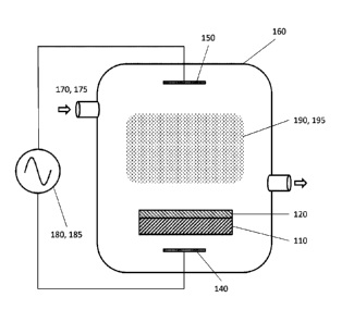
[0008] FIG. 1 illustrates a setup for producing an AR textured surface
according to one
embodiment of the present disclosure.
[0009] FIG. 2A illustrates a thin film deposited on a substrate, and FIG.
2B illustrates the
texture created in the thin film according to one embodiment of the present
disclosure.
[0010] FIG. 3A illustrates a thin film deposited on a substrate, FIG. 3B
illustrates the
texture created in the thin film, and FIG. 3C illustrates the texture
transferred to the substrate
according to one embodiment of the present disclosure.
DETAILED DESCRIPTION
[0011] The description of illustrative embodiments according to principles
of the present
disclosure is intended to be read in connection with the accompanying
drawings, which are to be
considered part of the entire written description. In the description of
embodiments of the
disclosure herein, any reference to direction or orientation is merely
intended for convenience of
description and is not intended in any way to limit the scope of the present
disclosure. Relative
terms such as "lower," "upper," "horizontal," "vertical," "above," "below,"
"up," "down," "top"
and "bottom" as well as derivative thereof (e.g., "horizontally,"
"downwardly," "upwardly," etc.)
should be construed to refer to the orientation as then described or as shown
in the drawing under
discussion. These relative terms are for convenience of description only and
do not require that
the apparatus be constructed or operated in a particular orientation unless
explicitly indicated as
such. Terms such as "attached," "affixed," "connected," "coupled,"
"interconnected," and similar
refer to a relationship wherein structures are secured or attached to one
another either directly or
indirectly through intervening structures, as well as both movable or rigid
attachments or
relationships, unless expressly described otherwise. Moreover, the features
and benefits of the
disclosure are illustrated by reference to the exemplified embodiments.
Accordingly, the disclosure
expressly should not be limited to such exemplary embodiments illustrating
some possible non-
- 4 -
Date Recue/Date Received 2023-08-01
limiting combination of features that may exist alone or in other combinations
of features; the
scope of the disclosure being defined by the claims appended hereto.
[0012] This disclosure describes the best mode or modes of practicing the
disclosure as
presently contemplated. This description is not intended to be understood in a
limiting sense, but
provides an example presented solely for illustrative purposes by reference to
the accompanying
drawings to advise one of ordinary skill in the art of the advantages and
construction of the certain
embodiments. In the various views of the drawings, like reference characters
designate like or
similar parts.
[0013] It is important to note that the embodiments disclosed are only
examples of the
many advantageous uses of the innovative teachings herein. In general,
statements made in the
specification of the present application do not necessarily limit any of the
various claimed
disclosures. Moreover, some statements may apply to some inventive features
but not to others.
In general, unless otherwise indicated, singular elements may be in plural and
vice versa with no
loss of generality.
[0014] FIG. 1 illustrates a schematic diagram of a system for fabricating
an AR structure
on the surface of a substrate according to an embodiment of the present
disclosure.
[0015] As shown in FIG. 2A, a thin film 120 is applied onto the substrate
110 in the initial
state. In the present context, it is understood that a thin film is a two
dimensional material layer
deposited on a substrate in order to achieve AR properties, and the thickness
of the thin film ranges
from nanometers to micrometers. Depending on the specific need of the optical
system, the thin
film thickness is selected to allow for the modification of the size, height,
and density of the
textured structures. FIG. 2B shows the final state where the textured
structures 125 is
manufactured on the thin film.
[0016] The substrate can be made of a large variety of materials commonly
used in optical
systems. For example, the material for the substrate may be selected from any
one or more of the
following: borosilicate glass, barium borate, barium fluoride calcite,
sapphire, calcium fluoride,
diamond, indium fluoride, magnesium fluoride, potassium bromide, zinc
selenide, germanium,
polytetrafluoroethylene, rutile, yttrium orthovanadate, zirconium fluoride.
The thin film material
- 5 -
Date Recue/Date Received 2023-08-01
can be silica, silicon, or a few other suitable/equivalent materials. Thus, a
unique advantage of an
embodiment of the present disclosure is that, because the thin film can be
applied to substrates
made of a large number of different materials, only common etching recipes
need to be developed
for a few thin film materials. In contrast, existing methods of etching
structures directly on a
substrate would require a different etching recipe for each substrate made of
a different material.
[0017] As shown in FIG. 1, after applying the thin film 120 to the surface
of the substrate
110, the coated substrate is placed between two electrodes 140, 150 of an
etching system 160. In
one embodiment, the etching system is a reactive ion etching (RIE) system, an
inductively coupled
plasma reactive ion etching (ICP-RIE) system or an ion beam sputtering system.
Gases 170 are
introduced into the reactive ion etching chamber 160 that contains the
electrodes 140, 150. A radio
frequency wave 180 is applied to the electrodes 140, 150 to ionize the gases
170 and create a
plasma 190 between the electrodes 140, 150. The plasma 190 chemically and
physically etches
the exposed thin film material and simultaneously deposits nanoscale polymer
islands on the thin
film surface.
[0018] In one embodiment, the gases include a mixture of gases selected
from Argon,
Helium, H2, 02, CH4, CHF3, CF4, C4F8, SF6, C12, F2, BC13, and SiC14.
[0019] Note that the plasma does not chemically etch the deposited
polymer, which
prevents the removal of topcoat material that is covered under the polymer.
The energetic ions
driven by the potential difference between the electrodes physically remove
the thin film and
polymer materials, and the deposition and physical removal of the polymer
concurrently occur on
the thin film surface.
[0020] The chemical and physical etching continues for a length of time to
produce
textured structures that are distributed on the thin film surface, and the
structures produced have
varied sizes, heights, and spacings. The length of time is based on the rate
of thin film removal
and rate of polymer deposition, and dimensions of the desired structure.
[0021] In one embodiment, the textured structures reduce the reflection of
incident light
through the thin film to less than or equal to 0.25%, and the textured
structures reduce the reflection
- 6 -
Date Recue/Date Received 2023-08-01
of incident light through the substrate surface to less than or equal to 0.25%
+ (¨ns-nt)2, where ns
ns+nt
and nt are the refractive indices of the substrate and thin film respectively.
[0022] In another embodiment of the present disclosure, the thin film is
used as a sacrificial
layer. As shown in FIG. 3A, a thin film 120 is applied onto the substrate 110
in the initial state.
FIG. 3B shows the intermediate state with textured structures 125 on the
sacrificial thin film. FIG.
3C shows the final state where the textured structure 115 is transferred to
the substrate.
[0023] Referring to FIG. 1 again, the first part of the process is similar
to the embodiment
shown in FIG. 2. After applying the thin film 120 to the surface of the
substrate 110, the substrate
is placed between two electrodes 140, 150 of a reactive ion etching system
160. Gases 170 are
introduced into the reactive ion etching chamber 160 that contains the
electrodes 140, 150. A radio
frequency wave 180 is applied to the electrodes 140, 150 to ionize the gases
and create a plasma
190 between the electrodes. The plasma chemically and physically etches the
exposed thin film
material and simultaneously deposits nanoscale polymer islands on the thin
film surface.
[0024] Upon arriving to the intermediate state shown in FIG. 3B, one or
more gases 175
are injected into the etching chamber 160. One or more radio frequency waves
185 are applied to
the electrodes 140, 150 of the etching chamber 160 to ionize the gases 175 and
create a high-
density plasma 195 between the electrodes 140, 150. In one embodiment, the
etching system is a
reactive ion etching (RIE) system, an inductively coupled plasma reactive ion
etching (ICP-RIE)
system or an ion beam sputtering system. In one embodiment, FIG. 1 shows the
same etching
system is used for manufacturing both the intermediate state and the final
state. It is contemplated
that the etching system used for manufacturing the intermediate state may be
different from the
etching system used for manufacturing the final state in another embodiment.
The high-density
plasma 195 removes the thin film and substrate materials concurrently. Note
that the textured thin
film structures 125 shield the substrate material underneath during the
etching until an area of the
thin film material is removed and the exposed substrate material is then
removed. The locations
of the substrate material being exposed follows the removal of the material of
the textured
structures of the thin film, and thus the profile of the substrate being
etched follows the profile of
the textured structures of the thin film. Thus, the textured structures of the
thin film act as a mask
- 7 -
Date Recue/Date Received 2023-08-01
for the substrate during the etching. The etching continues for a length of
time to transfer the
textured structures from the thin film to the substrate. The resulted
substrate having a textured
surface 115 is shown in FIG. 3C. Note that the textured structures of the
substrate may be made
more pronounced or obscured relative to the textured structures of the thin
film by adjusting the
ratio between the etch rate of the substrate material to the etch rate of the
thin film material.
[0025] In one embodiment, the textured structures in the substrate reduce
the reflection of
incident light through the substrate to 0.02 or smaller. In one embodiment,
the etching may be a
reactive ion etching. In one embodiment an inductively coupled plasma reactive
ion etching. In
one embodiment, the etching may be an ion beam sputtering.
[0026] In view of the foregoing, one or more embodiments of the present
disclosure
satisfies the long-felt need for a robust process to manufacture stable AR
coatings with wide
wavelength bands capable of withstanding high optical power, with low angular
sensitivity, and
weak polarization dependence. It also provides a unique advantage that the
process is relatively
independent of material or wavelength and capable of easily fabricating
structures for different
substrates.
[0027] While the present disclosure describes at some length and with some
particularity
with respect to the several described embodiments, it is not intended that it
should be limited to
any such particulars or embodiments or any particular embodiment, but it is to
be construed so as
to provide the broadest possible interpretation in view of the related art
and, therefore, to
effectively encompass various embodiments herein. Furthermore, the foregoing
describes various
embodiments foreseen by the inventor for which an enabling description was
available,
notwithstanding that modifications of the disclosure, not presently foreseen,
may nonetheless
represent equivalents thereto.
- 8 -
Date Recue/Date Received 2023-08-01