Note: Descriptions are shown in the official language in which they were submitted.
CA 03208511 2023-07-17
WO 2022/170086
PCT/US2022/015299
HIGH FIDELITY STORAGE AND RETRIEVAL OF QUANTUM INFORMATION
IN A WARM ATOMIC VAPOR CELL DEVICE
CROSS REFERENCE TO RELATED APPLICATIONS
This application claims the benefit under 35 U.S.C. 119(e) to U.S.
Provisional
Application No. 63/146,201, filed February 5, 2021, under Attorney Docket No.
Q0074.70006U500, titled "HIGH FIDELITY STORAGE AND RETRIEVAL OF
QUANTUM INFORMATION IN A WARM ATOMIC VAPOR CELL DEVICE," and U.S.
Provisional Application No. 63/245763, filed September 17, 2021, under
Attorney Docket No.
Q0074.70006U501, titled "HIGH FIDELITY STORAGE AND RETRIEVAL OF
QUANTUM INFORMATION IN A WARM ATOMIC VAPOR CELL DEVICE," both of
which are incorporated herein by reference in their entirety.
FEDERALLY SPONSORED RESEARCH
This invention was made with government support under DE-SC0019702 awarded by
the United States Department of Energy. The government has certain rights in
the invention.
BACKGROUND
Quantum networks facilitate the transmission of information in the form of
quantum
bits ("qubits") between physically separated quantum processors or other
quantum devices
(e.g., quantum sensors). Quantum networks may be used to enable optical
quantum
communication over distances and can be implemented over standard
telecommunication
optical fibers through the transmission of single photons onto which
information is encoded
(e.g., in polarization). To enable the reliable transmission of quantum
information over any
distances, additional components may be needed.
SUMMARY
The following is a non-limiting summary of some embodiments of the present
application. Some aspects of the present application are directed to a quantum
memory device.
The quantum memory device comprises: a first optical component configured to
convert an
input qubit encoded in an arbitrary polarization state of a photon into a
spatial qubit propagating
in a pair of parallel optical rails; an atomic vapor memory coupled to an
output of the first
optical component and configured to store the spatial qubit in an atomic
vapor; and a second
optical component coupled to an output of the atomic vapor memory, the second
optical
1
CA 03208511 2023-07-17
WO 2022/170086
PCT/US2022/015299
component configured to convert the spatial qubit, when retrieved from the
atomic vapor
memory, into an output qubit, the output qubit encoded in the arbitrary
polarization state of a
photon.
In some embodiments, the first optical component and/or the second optical
component
are a Sagnac-like device that comprises: a polarization beam splitter (PBS); a
first variable
angle mirror optically coupled to a first output of the PBS; and a second
variable angle mirror
optically coupled to a second output of the PBS. In some embodiments, the
first variable angle
mirror is disposed at a first angle relative to the polarization beam
splitter, and the second
variable angle mirror is disposed at a second angle relative to the
polarization beam splitter,
wherein the second angle is different than the first angle. In some
embodiments, changing the
first and/or second angle causes a change in a separation between optical
rails of the pair of
parallel optical rails.
In some embodiments, the quantum memory device further comprises a Bragg
grating
filter optically coupled to an input of the first optical component.
In some embodiments, the quantum memory device further comprises a pair of
flat
etalon cavities optically coupled to an output of the second optical
component. In some
embodiments, the flat etalon cavities of the pair of flat etalon cavities are
arranged with their
incident faces at a small off-parallel angle. In some embodiments, the quantum
memory device
further comprises at least three mirrors configured to cause the output qubit
to pass through the
pair of flat etalon cavities at least twice.
In some embodiments, the quantum memory device further comprises a pair of
curved
etalon cavities optically coupled to an output of the second optical
component.
Some aspects of the present application are directed to a method of storing
and
retrieving a qubit. The method comprises: receiving a qubit encoded in an
arbitrary polarization
state of a photon; converting, using a first optical component comprising a
Sagnac-like
configuration of optical elements, the qubit into a spatial qubit propagating
in a pair of parallel
optical rails; storing the spatial qubit in an atomic vapor memory; retrieving
and outputting the
spatial qubit from the atomic vapor memory; reconverting, using a second
optical component
comprising a Sagnac-like configuration of optical elements, the spatial qubit
into the qubit
encoded in the arbitrary polarization state; and outputting the qubit.
In some embodiments, converting the qubit into a spatial qubit comprises:
receiving the
qubit at a polarization beam splitter (PBS); converting the qubit into the
spatial qubit using the
PBS; directing the spatial qubit back through the PBS using a first variable
angle mirror and a
2
CA 03208511 2023-07-17
WO 2022/170086
PCT/US2022/015299
second variable angle mirror; and outputting, from the PBS, the spatial qubit
to a pair of parallel
optical rails.
In some embodiments, the first variable angle mirror is disposed at a first
angle relative
to the PBS, the second variable angle mirror is disposed at a second angle
relative to the PBS,
and the method further comprises changing a spacing between rails of the pair
of parallel
optical rails by changing the first and/or the second angle.
In some embodiments, the method further comprises changing a coherence time
for
storage of the qubit by: increasing the spacing between rails of the pair of
parallel optical rails;
and increasing a diameter of each rail of the pair of parallel optical rails
incident to the atomic
vapor memory.
In some embodiments, the method further comprises combining a pair of control
field
beams with respective rails of the pair of optical rails prior to storing the
spatial qubit in the
atomic vapor memory.
In some embodiments, the method further comprises filtering an input control
field
beam using a Bragg grating filter.
In some embodiments, the method further comprises, after outputting the qubit:
passing
the qubit in a first instance and in a first direction through two flat
etalons, the two flat etalons
being arranged with their incident faces at a small off-parallel angle; and
passing the qubit in a
second instance and in the first direction through the two flat etalons. In
some embodiments,
passing the qubit in the second instance through the two flat etalons
comprises using three or
more mirrors to steer the qubit. In some embodiments, the qubit, in the first
instance, passes
through the two flat etalons at a first location to one side of a central axis
of the two flat etalons;
and the qubit, in the second instance, passes through the two flat etalons at
a second location
to another side of the central axis. In some embodiments, passing the qubit
through the two flat
etalons in the first and second instances achieves an extinction ratio of
greater than or equal to
100dB and less than or equal to 150dB.
In some embodiments, the method further comprises, after outputting the qubit:
passing
the qubit in a first direction through two curved etalons, the two curved
etalons being arranged
with their incident faces at a small off-parallel angle.
BRIEF DESCRIPTION OF DRAWINGS
The accompanying drawings are not intended to be drawn to scale. In the
drawings,
each identical or nearly identical component that is illustrated in various
figures is represented
3
CA 03208511 2023-07-17
WO 2022/170086
PCT/US2022/015299
by a like numeral. For purposes of clarity, not every component may be labeled
in every
drawing. In the drawings:
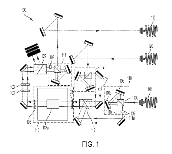
FIG. 1 shows a schematic diagram of a device 100 configured to store and
retrieve
qubits using a light-matter interface, in accordance with some embodiments of
the technology
described herein.
FIG. 2 is a schematic diagram of a device 200 configured to reduce noise
present in the
control laser beam before it enters the quantum memory, in accordance with
some
embodiments of the technology described herein.
FIG. 3 shows a schematic diagram of a device 300 configured to filter the
optical signal
retrieved from device 100 of FIG. 1, in accordance with some embodiments of
the technology
described herein.
FIG. 4 shows a schematic diagram of another device 400 configured to filter
the optical
signal retrieved from device 100 of FIG. 1, in accordance with some
embodiments of the
technology described herein.
FIG. 5 is a flowchart describing a process 500 for storing and retrieving a
qubit, in
accordance with some embodiments of the technology described herein.
FIG. 6A is a plot showing the effect of beam diameter on the coherence time of
qubit
storage of the atomic vapor memory of the light-matter interface, in
accordance with some
embodiments of the technology described herein.
FIG. 6B is a plot showing the effect of atomic vapor cell vapor pressure on
the
coherence time of the atomic vapor memory of the light-matter interface, in
accordance with
some embodiments of the technology described herein.
FIGs. 7A and 7B are plots showing the storage efficiency as a function of
storage time
for the left and right optical rails, in accordance with some embodiments of
the technology
described herein.
FIG. 8 is a plot showing the classical fidelity over time of the atomic vapor
memory of
the light-matter interface, in accordance with some embodiments of the
technology described
herein.
FIG. 9 is a plot showing the signal-to-noise ratio (SNR) of retrieved photons
from the
.. atomic vapor memory of the light-matter interface, in accordance with some
embodiments of
the technology described herein.
4
CA 03208511 2023-07-17
WO 2022/170086
PCT/US2022/015299
DETAILED DESCRIPTION
Room temperature quantum memories are used in quantum network architectures,
allowing for the temporary storage and synchronization of photonic qubits
across the network.
To perform such functions, the quantum memory receives and coherently stores
any random
input qubit without damaging the information encoded on the qubits. The
inventors have
recognized and appreciated that qubits having an arbitrary polarization may be
stored by
separating the vertical and/or horizontal polarization components of the
qubits into independent
optical beams ("rails"). The separated vertical and horizontal components may
then be
recombined into a single optical beam after retrieval from storage.
Accordingly, a dual rail quantum memory system is described herein. The dual
rail
quantum memory uses optical elements arranged in a Sagnac-like configuration
with
mismatched mirror angles to separate, and after retrieval, combine the
vertical and horizontal
polarization components of the qubits. In a traditional Sagnac configuration,
identical
overlapping optical paths are provided for an optical beam that has been split
into two. The
inventors have recognized and appreciated that these two beams may be
separated, rather than
overlapped, by a distance defined by the mirror angles in the Sagnac-like
configuration. The
beams may be separated by placing the mirrors of the Sagnac-like configuration
at two slightly
different angles (e.g., the angles may have a mismatch in range from 0 to 10,
2 , 5 , and/or
10 ). This arrangement allows for a tunable separation between the two optical
beams. This
tunability supports the use of different beam diameters, enabling, in turn, a
tunable coherence
time for the memory.
Accordingly, the inventors have developed a quantum memory device configured
to
store and retrieve qubits from an atomic vapor memory. The quantum memory
device includes
a first optical component (e.g., a Sagnac-like configuration) configured to
convert an input
qubit encoded in an arbitrary polarization state of a photon into a spatial
qubit propagating in
a pair of parallel optical rails. The quantum memory device includes an atomic
vapor memory
(e.g., including one or more atomic vapor cells) coupled to an output of the
first optical
component and configured to store the spatial qubit in an atomic vapor.
Thereafter, the spatial
qubit may be retrieved from the atomic vapor memory and output to a second
optical
component configured to convert the spatial qubit into an output qubit, the
output qubit encoded
in the arbitrary polarization state of a photon. The first optical component
and/or the second
optical components are Sagnac-like devices that include a polarization beam
splitter (PBS) and
two variable angle mirrors optically coupled to two outputs of the PBS.
5
CA 03208511 2023-07-17
WO 2022/170086
PCT/US2022/015299
The inventors have further developed an optical frequency filtering mechanism
that
achieves a high extinction (>120dB) of the control field laser beam after
retrieval of the qubits
from the quantum memory. The optical filtering mechanism achieves this high
extinction value
by passing the light through low finesse flat etalons twice. Passing the light
through the flat
etalon cavities twice provides improved stability to thermal and mechanical
alignment
perturbations of the quantum memory.
Following below are more detailed descriptions of various concepts related to,
and
embodiments of, techniques for implementing dynamic polarization drift
correction for
quantum telecommunications systems. It should be appreciated that various
aspects described
herein may be implemented in any of numerous ways. Examples of specific
implementations
are provided herein for illustrative purposes only. In addition, the various
aspects described in
the embodiments below may be used alone or in any combinations and are not
limited to the
combinations explicitly described herein.
FIG. 1 shows a schematic diagram of optical device 100, in accordance with
some
embodiments of the technology described herein. The optical device 100 forms a
quantum
memory layer from which photons with qubits (e.g., of arbitrary polarization)
can be stored
and retrieved on demand. In FIG. 1, input 101 is an input port in which qubits
(e.g., encoded
in the polarization of a photon or photons) enter device 100. Device 100
includes a number of
waveplates 102 and 103 configured to adjust the polarization of the qubits
and/or the control
field.
In some embodiments, the qubits travel from input 101 to module 110. Module
110 is
a mixed-angle Sagnac interferometer that converts a received qubit encoded in
the polarization
state of a photon into a spatial qubit propagating along parallel optical
rails 111a and 111b.
Module 110 may encode the spatial qubit into the amplitude and the phase of
the superposition
of a single photon propagating along the parallel optical rails 111a and 111b.
For example, if
the received qubit were encoded in an arbitrary polarization state of all-I) +
bete IV), the spatial
qubit output by the module 110 is encoded in the spatial state of all) + bete
IR), where IL) and
IR ) are the left and right rails, respectively, and /39 is the phase.
In some embodiments, module 110 includes a polarization beam splitter (PBS)
110a
and two variable angle mirrors 110b and 110c. The angle between the two
variable angle
mirrors 110b and 110c defines the separation between the two optical rails
111a and 111b after
the photons exit module 110. Changing the separation between the two optical
rails 111a and
111b changes the coherence time of the quantum memory. Preferably, the
separation between
6
CA 03208511 2023-07-17
WO 2022/170086
PCT/US2022/015299
the two optical rails 111a and 111b may be changed such that the coherence
time of the
quantum memory is maximized without causing the two optical rails 111a and
111b to overlap
spatially.
In some embodiments, after the pair of spatial qubits exit module 110, they
enter device
112. Device 112 is configured to redirect the spatial qubit into the light-
matter interface 113.
In some embodiments, device 112 may be a polarization beam splitter (e.g., a
Glan-Taylor
polarizer). The light-matter interface 113 includes one or more atomic vapor
cells 113a
configured to store the quantum information carried by the pair of spatial
qubits. For example,
the one or more atomic vapor cells 113a may include a vapor of certain
isotopes that can absorb
and store the quantum information (e.g., atoms of 87Rb, atoms of Cs, or atoms
of any other
suitable alkali metal). The atomic vapor cells 113a may be enclosed in a
temperature-controlled
and magnetically-shielded container (e.g., formed of Mu-metal). It should be
appreciated that
though the illustration of FIG. 1 shows only a single atomic vapor cell 113a,
the device 100
may include more than one (e.g., two, three, four, etc.) atomic vapor cells
113a, as aspects of
this technology are not limited in this respect.
In some embodiments, after the qubit is stored in the atomic vapor cell 113a,
the qubit
may be retrieved from the atomic vapor cell 113a and directed to module 114 by
polarization
beam splitter 122. Module 114 is a mixed-angle Sagnac interferometer
configured to map the
spatial qubit into a polarization qubit (e.g., into a photon with the qubit
encoded in an arbitrary
polarization state). A final set of mirrors directs the polarization qubit to
the output port 115,
where device 100 outputs retrieved polarization qubits.
In some embodiments, device 100 includes a control field input 120. Control
field input
120 is an input port for a control field laser beam. The control field laser
beam is configured to
control the process of storing and retrieving the qubits from device 100.
Control qubits are
directed from the control field input 120 to module 121. Module 121 is also a
mixed-angle
Sagnac interferometer like module 110. Module 121 is configured to split the
received control
field qubits into two identical, but spatially-separated, control field beams.
Device 112
combines the two control field beams received from module 121 with the pair of
spatial qubits
(e.g., optical rails 111a and 111b) before the qubits enter the light-matter
interface 113. When
qubits are retrieved from the light-matter interface 113, polarization beam
splitter 122 separates
the control field beams from the retrieved qubits with a success rate of
approximately 50dB.
The vast majority of the control beam is eliminated from the retrieved data
qubits after
polarization beam splitter 122.
7
CA 03208511 2023-07-17
WO 2022/170086
PCT/US2022/015299
FIG. 2 is a schematic diagram of a device 200 configured to reduce noise
present in the
control field laser beam before it enters the quantum memory, in accordance
with some
embodiments of the technology described herein. Device 200 is configured to
reduce
broadband noise in the control field laser beam. In particular, device 200 is
configured to reduce
broadband noise caused by the laser's amplified spontaneous emission (ASE) and
Raman
scattering that occurs as the control field laser beam propagates along
optical fibers that enter
the device 100.
In some embodiments, device 200 includes an input 201 and an output 204. The
control
field laser beam enters device 200 through the input 201 and exits the device
200 through the
output 204. Output 204 of the device 200 may be coupled to the control field
input 120 of
device 100 such that device 200 provides the control field laser beam to the
device 100. Output
204 may be optically coupled to the control field input 120 by, for example, a
short optical
fiber link or through a free space optical connection.
In some embodiments, device 200 includes a filter 202. The filter 202 may be a
Bragg
grating filter configured to reflect light within a narrow frequency band
(e.g., approximately
GHz wide). In some embodiments, filter 202 may be passively adjusted to remain
resonant
with the control field laser beam's central frequency mode, thereby minimizing
any laser or
Raman emission outside of the control field laser's transmission peak from
being transmitted
out of device 200.
20 In some embodiments, device 200 includes a cavity 203 that is
optically coupled to an
output of filter 202. The cavity 203 may be a passive filtering cavity (e.g.,
a Fabry-Perot etalon
cavity, a cavity having a frequency bandwidth of approximately 500 MHz). The
cavity 203
may be stabilized, for example, using a PID-controlled temperature controller
that encases the
cavity 203. The cavity 203 is tuned to pass the central frequency mode of the
control field laser.
FIG. 3 shows a schematic diagram of a device 300 that is configured to filter
the optical
signal retrieved from device 100 as described in connection with FIG. 1
herein, in accordance
with some embodiments of the technology described herein. The device 300
includes an input
301 and an output 304. The input 301 may be optically coupled (e.g., using an
optical fiber or
through free space) to the output 115 of device 100.
In some embodiments, the device 300 includes etalon cavities 302a and 302b.
The
etalon cavities 302a, 302b may be low finesse (e.g., having a finesse value of
approximately
30) flat etalon cavities that offer high robustness against temperature
fluctuations and are
significantly less sensitive to the laser alignment compared to conventional
curved etalons. In
some embodiments, the light received by the etalon cavities 302a and 302b may
be received
8
CA 03208511 2023-07-17
WO 2022/170086
PCT/US2022/015299
with a slight incident angle. This incident angle eliminates the need for
isolation between the
two etalon cavities 302a and 302b. In some embodiments, this angle may be
greater than 00
and less than 10 , 5 , 2 , and/or 1 .
In some embodiments, after the light passes through the etalon cavities 302a
and 302b
in a first instance, the light may be redirected back through the etalon
cavities 302a and 302b
for further filtering. For example, three mirrors 303a, 303b, and 303c may be
used to redirect
the light back through etalon cavities 302a and 302b for further filtering. By
passing the light
through the etalon cavities 302a and 302b twice, the light may be effectively
filtered by four
etalon cavities. The repeated filtering compensates for the low finesse of the
cavities and
provides an extinction value in a range from 100dB to 150dB on the remaining
control field
accompanying the qubits. Accordingly, when the qubits exit the device 300 at
output 304, the
qubits may have a signal to noise ratio (SNR) greater than or equal to 10 and
less than or equal
to 100.
FIG. 4 shows a schematic diagram of a device 400 that is configured to filter
the optical
signal retrieved from device 100 as described in connection with FIG. 1
herein, in accordance
with some embodiments of the technology described herein. The device 400
includes an input
401 and an output 404. The input 401 may be optically coupled (e.g., using an
optical fiber or
through free space) to the output 115 of device 100.
In some embodiments, the device 400 includes etalon cavities 402a and 402b.
The
etalon cavities 402a, 402b may be curved etalon cavities. In some embodiments,
the light
received by the etalon cavities 402a and 402b may be received with a slight
incident angle.
This incident angle eliminates the need for isolation between the two etalon
cavities 402a and
402b. In some embodiments, this angle may be greater than 0 and less than 10
, 5 , 2 , and/or
1 . The etalon cavities 402a, 402b may provide an extinction value in a range
from 100dB to
150dB on the remaining control field accompanying the qubits. Accordingly,
when the qubits
exit the device 400 at output 404, the qubits may have a signal to noise ratio
(SNR) greater
than or equal to 10 and less than or equal to 100, as described in connection
with FIG. 9 herein.
FIG. 5 is a flowchart describing a process 500 for storing and retrieving a
qubit, in
accordance with some embodiments of the technology described herein. Process
500 may be
performed, for example, using optical device 100 as described in connection
with FIG. 1 herein,
in some embodiments.
Process 500 may begin at act 502, in which a qubit encoded in an arbitrary
polarization
state of a photon is received. For example, the arbitrary polarization state
lip) of the photon
may be described by:
9
CA 03208511 2023-07-17
WO 2022/170086
PCT/US2022/015299
10) = + bete IV),
where IH) and IV) are the horizontal and vertical polarization basis states
and /39 is the phase
of the photon.
In some embodiments, the qubit may be received by the optical device over an
optical
fiber connection. For example, the qubit may be received over
telecommunications optical fiber
from a qubit source located a distance (e.g., kilometers) away from the
optical device.
Alternatively, in some embodiments the qubit may be received over optical
fiber or through
free space from a qubit source co-located with the optical device (e.g., in a
same room as the
optical device, in a same facility as the optical device).
After act 502, process 500 may proceed to act 504 in some embodiments. At act
504,
the received qubit may be converted into a spatial qubit propagating in a pair
of parallel optical
rails. The received qubit may be converted using a first optical component
comprising a
Sagnac-like configuration of optical elements. For example, the first optical
component may
be module 110 of optical device 100 as described in connection with FIG. 1
herein.
In some embodiments, converting the qubit into a spatial qubit may include
receiving
the qubit at a polarization beam splitter (PBS; e.g., PBS 110a) and converting
the qubit into the
spatial qubit using the PBS. For example, the PBS may encode the arbitrary
polarization state
of the received qubit into a spatial qubit output encoded in the spatial state
of all) + bete IR) ,
where IL) and IR ) are the left and right rails, respectively.
In some embodiments, directing the spatial qubit back through the PBS using
first and
second variable angle mirrors (e.g., variable angle mirrors 110b, 110c) may
physically separate
the two beams into a pair of parallel optical rails. The degree of physical
separation of the
optical rails (e.g., a spacing between the optical rails) may be adjusted by
changing a relative
angle of the first and/or second variable angle mirrors with respect to the
PBS. After the parallel
optical rails are separated, the spatial qubit may be output from the PBS and
from the first
optical component.
After act 504, process 500 may proceed to act 506, in some embodiments. At act
506,
the spatial qubit may be stored in an atomic vapor memory. For example, the
spatial qubit may
be stored using light-matter interface 113 as described in connection with
FIG. 1 herein. The
atomic vapor memory may include one or more atomic vapor cells. The one or
more atomic
vapor cells 113a may include a vapor of certain isotopes that can absorb and
store the quantum
information (e.g., atoms of 87Rb, atoms of Cs, or atoms of any other suitable
alkali metal). The
atomic vapor cells 113a may be enclosed in a temperature-controlled and
magnetically-
CA 03208511 2023-07-17
WO 2022/170086
PCT/US2022/015299
shielded container (e.g., formed of Mu-metal). In some embodiments, the
parallel optical rails
may be combined with a pair of control field beams before the spatial qubit is
stored in the
atomic vapor memory.
In some embodiments, a coherence time for storage of the qubit may be tuned.
For
example, the coherence time may be tuned by increasing the spacing between
rails of the pair
of parallel optical rails (e.g., by changing an angle of the first and/or
second variable angle
mirrors with respect to the PBS of the first optical component). Alternatively
or additionally,
the coherence time may be tuned by changing a diameter of each rail of the
pair of parallel
optical rails incident to the atomic vapor memory.
After act 506, process 500 may proceed to act 508, in some embodiments. At act
508,
the spatial qubit may be retrieved and output from the atomic vapor memory.
After act 508, process 500 may proceed to act 510, in some embodiments. At act
510,
the spatial qubit may be reconverted into a qubit encoded in an arbitrary
polarization state of a
photon. The spatial qubit may be reconverted using a second optical component
comprising a
Sagnac-like configuration of optical elements. For example, the second optical
component may
be module 114 of optical device 100 as described in connection with FIG. 1
herein.
In some embodiments, reconverting the spatial qubit into the qubit may include
receiving the spatial qubit at a polarization beam splitter (PBS) and
converting the spatial qubit
into the qubit using the PBS. Another pair of variable angle mirrors may be
used to rejoin the
pair of parallel optical rails into a single beam for output.
After act 510, process 500 may proceed to act 512, in some embodiments. At act
512,
the qubit may be output. For example, the qubit may be output into a fiber
optic cable using a
fiber optic connection. Alternatively, the qubit may be output into free space
using a free space
optical connection.
In some embodiments, after the qubit is output, the qubit may be further
filtered. For
example, the qubit may be passed through one or more etalon cavities. In some
embodiments,
the qubit may be passed through two curved etalons. The two curved etalons may
be arranged
with their incident faces at a small off-parallel angle.
Alternatively, in some embodiments, the qubit may be passed in a first
instance and
again in a second instance along a first direction through two flat etalons.
In the first instance,
the qubit may pass through the two flat etalons at a first location to one
side of a central axis
of the two flat etalons. In the second instance, the qubit may pass through
the two flat etalons
at a second location to another side of the central axis. Passing the qubit
through the two flat
etalons in the first and second instances may achieve an extinction ratio of
greater than or equal
11
CA 03208511 2023-07-17
WO 2022/170086
PCT/US2022/015299
to 100dB and less than or equal to 150dB. In some embodiments, three or more
mirrors may
be used to steer the qubit through the two flat etalons in the second
instance. The two flat
etalons may be arranged with their incident faces at a small off-parallel
angle.
FIG. 6A is a plot showing the effect of beam diameter on the coherence time of
qubit
storage of the atomic vapor memory of the light-matter interface, in
accordance with some
embodiments of the technology described herein. The plot shows normalized
efficiency on the
vertical axis and storage time in microseconds on the horizontal axis. Three
curves 601, 602,
and 603 are plotted. Each curve 601, 602, and 603 represents an exponential
fit to
measurements of the storage efficiency of a quantum memory (e.g., like optical
device 100 of
FIG. 1 herein) at different storage times for different beam diameters used in
the parallel optical
rails of the quantum memory. Curve 601 shows a fit to data acquired using a
beam at half of a
normalized diameter. Curve 602 shows a fit to data acquired using a beam at a
normalized
diameter. Curve 603 shows a fit to data acquired using a beam at twice a
normalized diameter.
The data indicates that as the beam size increases from curve 601 to curve
603, both the
coherence time is increased. This data shows that the coherence time of a
quantum memory as
described herein may be tuned based on the beam size of the parallel optical
rails of the
quantum memory.
FIG. 6B is a plot showing the effect of atomic vapor cell vapor pressure on
the
coherence time of the atomic vapor memory of the light-matter interface, in
accordance with
some embodiments of the technology described herein. The plot shows normalized
efficiency
on the vertical axis and storage time in microseconds on the horizontal axis.
Three data sets
604, 605, and 606 are plotted. Each data set 604, 605, and 606 was acquired
for different values
of vapor pressure in the atomic vapor cells of the light-matter interface of
the quantum memory.
Data sets 604, 605, and 606 were acquired with a vapor pressure of 10 Torr, 20
Torr, and 30
Torr, respectively. The data indicates that as the vapor pressure increases
from data set 604 to
605, the coherence time is increased. This data shows that the coherence time
of a quantum
memory as described herein may be tuned based on the vapor pressure of the
atomic vapor
cells used in the quantum memory. Combining the effects of beam size and vapor
pressure,
coherence times in a range from 0.5 ms to 10 ms can be achieved.
FIGs. 7A and 7B are plots showing the storage efficiency as a function of
storage time
for the left and right optical rails, respectively, of a quantum memory in
accordance with some
embodiments of the technology described herein. The plots show storage
efficiency on the
vertical axis and storage time in microseconds on the horizontal axis. Curve
701 is an
exponential fit to data acquired from the left optical rail and curve 702 is
an exponential fit to
12
CA 03208511 2023-07-17
WO 2022/170086
PCT/US2022/015299
data acquired from the right optical rail. The coherence time may be extracted
from the fits of
curves 701 and 702 and is 157 8 [Ls for the left rail and 133 6 [Ls for
the right rail.
FIG. 8 is a plot showing the classical fidelity over time of the atomic vapor
memory of
the light-matter interface, in accordance with some embodiments of the
technology described
herein. The plot shows classical fidelity on the vertical axis and time in
minutes on the
horizontal axis. Data points 801 were collected by measuring the fidelity of
qubits stored in a
quantum memory as described herein at different retrieval times. Measured
fidelities are greater
than 99.4% up to 400 minutes after storage of the qubits.
FIG. 9 is a plot showing the signal-to-noise ratio (SNR) of retrieved photons
from the
atomic vapor memory of the light-matter interface, in accordance with some
embodiments of
the technology described herein. The plot shows the measured photon amplitude
on the vertical
axis and time in microseconds on the horizontal axis. The left peak 901 is due
to an input qubit
to the quantum memory, and the right peak 902 is due to the retrieval of the
qubit from the
quantum memory after 5 [Ls of storage. The measured SNR is approximately 10
for a dual rail
quantum memory or 20 for a single rail quantum memory (e.g., if polarization
does not need
to be stored). Such a high SNR results in a fidelity greater than 95%.
Various aspects of the embodiments described above may be used alone, in
combination, or in a variety of arrangements not specifically discussed in the
embodiments
described in the foregoing and is therefore not limited in its application to
the details and
arrangement of components set forth in the foregoing description or
illustrated in the drawings.
For example, aspects described in one embodiment may be combined in any manner
with
aspects described in other embodiments.
Use of ordinal terms such as "first," "second," "third," etc., in the claims
to modify a
claim element does not by itself connote any priority, precedence, or order of
one claim element
over another or the temporal order in which acts of a method are performed,
but are used merely
as labels to distinguish one claim element having a certain name from another
element having
a same name (but for use of the ordinal term) to distinguish the claim
elements.
Also, the phraseology and terminology used herein is for the purpose of
description and
should not be regarded as limiting. The use of "including," "comprising,"
"having,"
"containing," "involving," and variations thereof herein, is meant to
encompass the items listed
thereafter and equivalents thereof as well as additional items.
The word "exemplary" is used herein to mean serving as an example, instance,
or
illustration. Any embodiment, implementation, process, feature, etc. described
herein as
13
CA 03208511 2023-07-17
WO 2022/170086 PCT/US2022/015299
exemplary should therefore be understood to be an illustrative example and
should not be
understood to be a preferred or advantageous example unless otherwise
indicated.
Having thus described several aspects of at least one embodiment, it is to be
appreciated
that various alterations, modifications, and improvements will readily occur
to those skilled in
the art. Such alterations, modifications, and improvements are intended to be
part of this
disclosure and are intended to be within the spirit and scope of the
principles described herein.
Accordingly, the foregoing description and drawings are by way of example
only.
14